JP6259669B2 - Inspection device and measuring device - Google Patents
Inspection device and measuring device Download PDFInfo
- Publication number
- JP6259669B2 JP6259669B2 JP2014007429A JP2014007429A JP6259669B2 JP 6259669 B2 JP6259669 B2 JP 6259669B2 JP 2014007429 A JP2014007429 A JP 2014007429A JP 2014007429 A JP2014007429 A JP 2014007429A JP 6259669 B2 JP6259669 B2 JP 6259669B2
- Authority
- JP
- Japan
- Prior art keywords
- voltage
- output
- photon counting
- inspection
- counting sensor
- Prior art date
- Legal status (The legal status is an assumption and is not a legal conclusion. Google has not performed a legal analysis and makes no representation as to the accuracy of the status listed.)
- Expired - Fee Related
Links
Images


Classifications
-
- H—ELECTRICITY
- H01—ELECTRIC ELEMENTS
- H01J—ELECTRIC DISCHARGE TUBES OR DISCHARGE LAMPS
- H01J37/00—Discharge tubes with provision for introducing objects or material to be exposed to the discharge, e.g. for the purpose of examination or processing thereof
- H01J37/02—Details
- H01J37/244—Detectors; Associated components or circuits therefor
-
- A—HUMAN NECESSITIES
- A61—MEDICAL OR VETERINARY SCIENCE; HYGIENE
- A61B—DIAGNOSIS; SURGERY; IDENTIFICATION
- A61B5/00—Measuring for diagnostic purposes; Identification of persons
- A61B5/0059—Measuring for diagnostic purposes; Identification of persons using light, e.g. diagnosis by transillumination, diascopy, fluorescence
-
- G—PHYSICS
- G01—MEASURING; TESTING
- G01N—INVESTIGATING OR ANALYSING MATERIALS BY DETERMINING THEIR CHEMICAL OR PHYSICAL PROPERTIES
- G01N21/00—Investigating or analysing materials by the use of optical means, i.e. using sub-millimetre waves, infrared, visible or ultraviolet light
- G01N21/84—Systems specially adapted for particular applications
- G01N21/88—Investigating the presence of flaws or contamination
- G01N21/94—Investigating contamination, e.g. dust
-
- G—PHYSICS
- G01—MEASURING; TESTING
- G01N—INVESTIGATING OR ANALYSING MATERIALS BY DETERMINING THEIR CHEMICAL OR PHYSICAL PROPERTIES
- G01N21/00—Investigating or analysing materials by the use of optical means, i.e. using sub-millimetre waves, infrared, visible or ultraviolet light
- G01N21/84—Systems specially adapted for particular applications
- G01N21/88—Investigating the presence of flaws or contamination
- G01N21/95—Investigating the presence of flaws or contamination characterised by the material or shape of the object to be examined
- G01N21/9501—Semiconductor wafers
-
- G—PHYSICS
- G01—MEASURING; TESTING
- G01N—INVESTIGATING OR ANALYSING MATERIALS BY DETERMINING THEIR CHEMICAL OR PHYSICAL PROPERTIES
- G01N21/00—Investigating or analysing materials by the use of optical means, i.e. using sub-millimetre waves, infrared, visible or ultraviolet light
- G01N21/84—Systems specially adapted for particular applications
- G01N21/88—Investigating the presence of flaws or contamination
- G01N21/95—Investigating the presence of flaws or contamination characterised by the material or shape of the object to be examined
- G01N21/956—Inspecting patterns on the surface of objects
-
- H—ELECTRICITY
- H01—ELECTRIC ELEMENTS
- H01J—ELECTRIC DISCHARGE TUBES OR DISCHARGE LAMPS
- H01J37/00—Discharge tubes with provision for introducing objects or material to be exposed to the discharge, e.g. for the purpose of examination or processing thereof
- H01J37/26—Electron or ion microscopes; Electron or ion diffraction tubes
- H01J37/28—Electron or ion microscopes; Electron or ion diffraction tubes with scanning beams
-
- A—HUMAN NECESSITIES
- A61—MEDICAL OR VETERINARY SCIENCE; HYGIENE
- A61B—DIAGNOSIS; SURGERY; IDENTIFICATION
- A61B5/00—Measuring for diagnostic purposes; Identification of persons
- A61B5/0059—Measuring for diagnostic purposes; Identification of persons using light, e.g. diagnosis by transillumination, diascopy, fluorescence
- A61B5/0075—Measuring for diagnostic purposes; Identification of persons using light, e.g. diagnosis by transillumination, diascopy, fluorescence by spectroscopy, i.e. measuring spectra, e.g. Raman spectroscopy, infrared absorption spectroscopy
-
- H—ELECTRICITY
- H01—ELECTRIC ELEMENTS
- H01J—ELECTRIC DISCHARGE TUBES OR DISCHARGE LAMPS
- H01J2237/00—Discharge tubes exposing object to beam, e.g. for analysis treatment, etching, imaging
- H01J2237/244—Detection characterized by the detecting means
- H01J2237/2443—Scintillation detectors
-
- H—ELECTRICITY
- H01—ELECTRIC ELEMENTS
- H01J—ELECTRIC DISCHARGE TUBES OR DISCHARGE LAMPS
- H01J2237/00—Discharge tubes exposing object to beam, e.g. for analysis treatment, etching, imaging
- H01J2237/244—Detection characterized by the detecting means
- H01J2237/2444—Electron Multiplier
-
- H—ELECTRICITY
- H01—ELECTRIC ELEMENTS
- H01J—ELECTRIC DISCHARGE TUBES OR DISCHARGE LAMPS
- H01J2237/00—Discharge tubes exposing object to beam, e.g. for analysis treatment, etching, imaging
- H01J2237/244—Detection characterized by the detecting means
- H01J2237/2445—Photon detectors for X-rays, light, e.g. photomultipliers
-
- H—ELECTRICITY
- H01—ELECTRIC ELEMENTS
- H01J—ELECTRIC DISCHARGE TUBES OR DISCHARGE LAMPS
- H01J2237/00—Discharge tubes exposing object to beam, e.g. for analysis treatment, etching, imaging
- H01J2237/244—Detection characterized by the detecting means
- H01J2237/24495—Signal processing, e.g. mixing of two or more signals
-
- H—ELECTRICITY
- H01—ELECTRIC ELEMENTS
- H01J—ELECTRIC DISCHARGE TUBES OR DISCHARGE LAMPS
- H01J49/00—Particle spectrometers or separator tubes
Description
本発明は、検査装置および計測装置に関する。 The present invention relates to an inspection apparatus and a measurement apparatus.
本技術分野の背景技術として、特表2005−526239号公報(特許文献1)がある。この公報には、「半導体ウエハのような試料から発せられるビームからの(例えば散乱された光、反射された光、または二次電子)比較的大きなダイナミックレンジの強度値を検出するメカニズムを提供する。」と記載されている(要約参照)。 As background art of this technical field, there is JP 2005-526239 A (Patent Document 1). This publication provides “a mechanism for detecting relatively large dynamic range intensity values (eg, scattered light, reflected light, or secondary electrons) from a beam emitted from a sample such as a semiconductor wafer. (See summary).
また、特許文献2には、「複数の素子に直流電圧を供給する電圧調整装置であって、前記複数の素子の各高電位側端子に、第1電圧を供給する第1供給回路と、前記複数の素子の各低電位側端子に、それぞれ、前記第1電圧よりも小さい、前記複数の素子の特性に依存した複数の電圧を供給する第2供給回路と、を備える電圧調整装置」が記載されている。 Patent Document 2 states that “a voltage adjusting device that supplies a DC voltage to a plurality of elements, a first supply circuit that supplies a first voltage to each high-potential side terminal of the plurality of elements; A voltage regulator comprising: a second supply circuit that supplies a plurality of voltages depending on characteristics of the plurality of elements, which are smaller than the first voltage, to each low potential side terminal of the plurality of elements ”. Has been.
前記特許文献1には、ウエハ表面にビームを照射した際の、ウエハ表面上にある異物からの散乱光強度を比較的大きなダイナミックレンジで検出する仕組みが記載されている。しかし、特許文献1の装置では、例えば、ウエハ上の異物からの散乱光強度が、異物径に応じて微小になった場合には、センサから出力される検出信号にはセンサ素子自身の暗ノイズの占める割合が大きくなり、微小な異物の検出が困難となる。
上記の課題を解決するために、光検出手段として例えば、光子計数センサとしてMPPC(Multi-Pixel Photon Counter、浜松ホトニクス株式会社の登録商標)のような半導体光検出素子や、光電子増倍管が使用される。 In order to solve the above problems, for example, a semiconductor photodetection element such as MPPC (Multi-Pixel Photon Counter, a registered trademark of Hamamatsu Photonics) or a photomultiplier tube is used as a photon detection sensor as a photon detection sensor. Is done.
光子計数センサでは、特許文献2で述べられているように、半導体光検出素子が所定の光量の光入力に対して所定の電圧を出力するため、半導体光素子への印加電圧を調整する手段を光検出手段に配設する必要がある。 In the photon counting sensor, as described in Patent Document 2, since the semiconductor photodetecting element outputs a predetermined voltage in response to a predetermined amount of light input, means for adjusting a voltage applied to the semiconductor optical element is provided. It is necessary to arrange in the light detection means.
また、レーザ光源がパルス発振しているため、高速で繰り返される散乱光入射に対して光子計数センサの応答速度が不足すると、光子計数センサで検出される信号成分が低下し、微小異物の高精度検出が困難となる。 In addition, since the laser light source oscillates, if the response speed of the photon counting sensor is insufficient for incident light scattered repeatedly at a high speed, the signal component detected by the photon counting sensor is lowered, and high precision of minute foreign matters is obtained. Detection becomes difficult.
さらに、光子計数センサは、光検出素子が数百ピクセル以上に細分化して配置されており、各光検出素子の増倍率がデバイス上で部分ごとに偏る可能性がある。この場合、光子計数センサからの出力電流が光入射部分に応じてばらつくため、出力電流値から光子数が弁別出来ず、今後、数個レベルでの光子を計数する、より高度な微小異物の高精度検出が困難となる、という課題を有している。 Furthermore, in the photon counting sensor, the photodetecting elements are subdivided into several hundred pixels or more, and there is a possibility that the multiplication factor of each photodetecting element is biased for each part on the device. In this case, since the output current from the photon counting sensor varies depending on the light incident part, the number of photons cannot be discriminated from the output current value. There is a problem that accuracy detection becomes difficult.
そこで、本発明は、光子計数センサにおいて微小異物を高精度に検出する検出回路およびそれを用いた検査装置、計測装置を提供する。 Therefore, the present invention provides a detection circuit that detects a minute foreign matter with high accuracy in a photon counting sensor, and an inspection device and a measurement device using the detection circuit.
上記課題を解決するために、例えば特許請求の範囲に記載の構成を採用する。 In order to solve the above problems, for example, the configuration described in the claims is adopted.
本願は上記課題を解決する手段を複数含んでいるが、その一例を挙げるならば、試料表面を検査または計測する検査または計測装置であって、前記試料表面にレーザビームを照射する照射手段と、前記試料表面からの散乱光を検出して検出信号を生成する検出手段と、を備え、前記検出手段は、Nピクセル(Nは自然数)の光検出素子から、M個(Mは自然数、M<N)の出力信号を出力する光子計数センサと、前記光子計数センサの出力信号をそれぞれ電流電圧変換するM個の電流電圧変換手段と、前記電流電圧変換手段に基準電圧を印加する電圧印加手段と、前記電流電圧変換手段の出力に基づいて検出信号を生成する検出信号生成手段と、を有することを特徴とする。 The present application includes a plurality of means for solving the above-described problems. To give an example, an inspection or measurement apparatus for inspecting or measuring the sample surface, the irradiation means for irradiating the sample surface with a laser beam, Detecting means for detecting scattered light from the sample surface and generating a detection signal, wherein the detecting means includes M (M is a natural number, M < N) a photon counting sensor for outputting an output signal, M current-voltage converting means for current-voltage converting the output signals of the photon counting sensor, and a voltage applying means for applying a reference voltage to the current-voltage converting means. And detection signal generation means for generating a detection signal based on the output of the current-voltage conversion means.
本発明によれば、光子計数センサにおいて微小な異物を高精度に検出することができる。 According to the present invention, a minute foreign matter can be detected with high accuracy in a photon counting sensor.
上記した以外の課題、構成及び効果は、以下の実施形態の説明により明らかにされる。 Problems, configurations, and effects other than those described above will be clarified by the following description of embodiments.
以下、実施例を図面を用いて説明する。 Hereinafter, examples will be described with reference to the drawings.
光子計数センサは、半導体検査または計測装置や、医用・医療装置など分野で幅広く応用されている。例えば、半導体検査または計測装置は、検査または計測対象のウエハに電子ビームをスキャンして照射し、発生する二次電子をシンチレーションで光に変換し、この光を光子計数センサで信号検出して計測や検出画像を生成し、計測や検出画像に基づいて、検査または計測を行う装置である。この半導体検査または計測装置を用いて、半導体を検査または計測する場合には、製造過程における異常や不良の発生を早期に、あるいは事前に検知するため、各製造工程の終了時において半導体上のパターンの検査または計測が行われる。 Photon counting sensors are widely applied in fields such as semiconductor inspection or measurement devices, medical / medical devices, and the like. For example, a semiconductor inspection or measurement device scans and irradiates a wafer to be inspected or measured with an electron beam, converts the generated secondary electrons into light by scintillation, detects this light with a photon counting sensor, and measures it. Or a detection image is generated, and an inspection or measurement is performed based on the measurement or detection image. When semiconductors are inspected or measured using this semiconductor inspection or measurement device, the pattern on the semiconductor is detected at the end of each manufacturing process in order to detect abnormalities and defects in the manufacturing process early or in advance. Inspection or measurement is performed.
本実施例では、微小異物の高精度検出のために、レーザ光源のパルス発振に対する光子計数センサの高速応答を実現するとともに、デバイス上の光像倍率のばらつきを抑制する検査装置の例を説明する。 In the present embodiment, an example of an inspection apparatus that realizes a high-speed response of a photon counting sensor with respect to pulse oscillation of a laser light source and suppresses variation in optical image magnification on the device for high-precision detection of minute foreign matters will be described. .
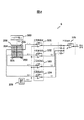
図1は、本実施例の検査装置の構成図の例である。 FIG. 1 is an example of a configuration diagram of an inspection apparatus according to the present embodiment.
検査装置50は、レーザ2、反射板3、レンズ4、5、センサ6、増幅回路7、A/D変換回路8、データ処理部9、CPU10、マップ出力部11、ステージ制御部12、回転ステージ13、並進ステージ14、クロック検出部20、遅延制御部24を有する。
The
異物検査装置50では、ウエハ1を回転ステージ13上に設置して、レーザ光源2から出力されるレーザ光を反射板3とレンズ4を介してウエハ1上に照射する。このとき、異物検査装置50では、CPU10の制御によりステージ制御部12を介して、ウエハ1を回転ステージ13で回転動作させるとともに、並進ステージ14で直線動作させる。これにより、ウエハ1上に照射されるレーザ光は、ウエハ1の全面でらせん状の軌跡となり、ウエハ1の全表面を検査することができる。
In the foreign
クロック検出部20は、センサ21、IV変換回路22、クロック再生回路23を有し、反射板3を透過したレーザ光を元に、レーザ光源2に同期したクロック信号を生成する。
The
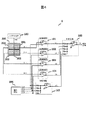
本実施例による検査装置50では、クロック検出部20で生成されたクロック信号を、遅延調整部24を介して遅延調整し、これに基づいてセンサ6が出力する検出信号を増幅回路7で増幅し、A/D変換回路8でサンプリングする。 図2は、検査装置50におけるセンサ6の構成図の例、図3は本実施例における分子型格子計数センサ200の構成図の例である。
In the
センサ6は、光子計数センサ200、バイアス電圧設定手段100、IV変換回路101、102、103、104、加算回路105、電圧設定手段106を有する。光子計数センサ200は、Nピクセルの光検出素子を搭載しており、図3に図示したように、4つの領域201、202、203、204毎に出力を共通化して出力する。
The
IV変換回路101、102、103、104は、光子計数センサ200の領域201、202、203、204からの出力電流I1、I2、I3、I4を、それぞれ電圧V1、V2、V3、V4に変換し、加算回路105でIV変換回路101、102、103、104の出力を加算して検出信号Voを出力する。
The IV
電圧設定手段106は、IV変換回路101、102、103、104の基準電圧を制御し、その結果、光子計数センサ200の領域201、202、203、204には、バイアス電圧設定手段が出力した電圧Vb0と、電圧設定手段106が出力した電圧Vb1の差電圧が印加される。
The
IV変換回路101、102、103、104、および加算回路105の抵抗値をすべてRとすると、センサ6の出力電圧Voは、式1で与えられる。式1より、Vb1およびRは既知であり、Voを計測することで、光子計数センサ200の出力電流、すなわち光子計数センサへの入射光量を計測することが可能となる。
(式1) Vo=(I1+I2+I3+I4)・R−4・Vb1
このように、光子計数センサ200におけるNピクセルをM個の領域毎(N>M。M、Nともに自然数)に共通化し、それぞれ独立にIV変換回路で電圧に変換して加算出力することで、光子計数センサ200内部の寄生成分の影響を分散して、レーザ光源2のパルス発振に対する光子計数センサ200の高速応答を実現することが可能となる。
When the resistance values of the IV
(Formula 1) Vo = (I1 + I2 + I3 + I4) * R-4 * Vb1
In this way, by sharing the N pixels in the
そして、光子計数センサとして例えばMPPC(登録商標)を使用する場合、通常70V程度の高電圧を印加すると、数Vの電圧で増倍率が変動することが知られている。そこで、図2に図示した電圧設定手段106により基準電圧Vb1を各IV変換回路に印加することで、光子計数センサからの出力電流の、光入射部分に応じたばらつきを調整し、光子計数センサの増倍率を制御することができる。 When using, for example, MPPC (registered trademark) as a photon counting sensor, it is known that when a high voltage of about 70 V is applied, the multiplication factor varies with a voltage of several volts. Therefore, by applying the reference voltage Vb1 to each IV conversion circuit by the voltage setting means 106 shown in FIG. 2, the variation of the output current from the photon counting sensor according to the light incident portion is adjusted, and the photon counting sensor The multiplication factor can be controlled.
すなわち、本実施例の構成により光子計数センサにおいて、レーザ光源の高速パルス発振に対応し、かつ、数百ピクセル以上に細分化して配置された各光検出素子の増倍率のばらつきを抑制できるため、微小異物の高精度検出が可能となる。 なお、本実施例では、IV変換回路101〜104の全てに基準電圧Vb1を印加しているが、光入射領域毎のばらつきに応じて、各IV変換回路にそれぞれ異なる基準電圧を印加する構成であっても、光子計数センサの増倍率の制御が可能となる。
That is, in the photon counting sensor according to the configuration of the present embodiment, it is possible to suppress the variation in the multiplication factor of each photodetecting element that corresponds to the high-speed pulse oscillation of the laser light source and is divided into several hundred pixels or more. High precision detection of minute foreign matter is possible. In this embodiment, the reference voltage Vb1 is applied to all of the
本実施例では、光子計数センサが搭載される検査装置について説明したが、光子計数センサを搭載する装置はこれに限らず、半導体計測装置、または、質量分析装置でも良い。 In the present embodiment, the inspection apparatus on which the photon counting sensor is mounted has been described. However, the apparatus on which the photon counting sensor is mounted is not limited to this, and may be a semiconductor measuring apparatus or a mass spectrometer.
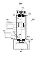
図6に半導体計測装置の構成図の例を示す。半導体計測装置300では、電子銃301で電子ビーム303を生成し、集束レンズ302、偏向制御部304、対物レンズ305を介して、ステージ307上にある半導体ウエハ306を電子ビーム303でスキャンする。半導体ウエハ306では電子ビーム303の照射により2次電子308が発生し、2次電子308はシンチレータ309、光子計数センサ310を介して検出され、データ処理部311で検出画像の生成と計測あるいは検査が行われる。
FIG. 6 shows an example of a configuration diagram of the semiconductor measuring device. In the
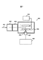
図7に質量分析装置の構成図の例を示す。質量分析装置では、試料をイオン化して真空チャンバ内の電極間に捕捉し、この電極に高電圧をスキャンして各電圧に応じた質量のイオンを放出し、これをシンチレーションで光に変換し、光子計数センサで信号検出して質量分析が行われる。質量分析装置400では、試料ガス401を試料導入室402に注入し、これをイオン化室403でイオン化する。イオン化された試料は、イオントラップ部404で捕捉され、ここに高電圧印加部405から高電圧をスキャンすることで各電圧に応じた質量のイオンがシンチレータ406と光子計数センサ407を介して検出され、データ処理部408で質量部分析が行われる。
FIG. 7 shows an example of a configuration diagram of the mass spectrometer. In a mass spectrometer, a sample is ionized and captured between electrodes in a vacuum chamber, a high voltage is scanned on this electrode to release ions of mass corresponding to each voltage, and this is converted into light by scintillation, Mass analysis is performed by detecting a signal with a photon counting sensor. In the
なお、光子計数センサが搭載される装置に関しては、以降の実施例においても、本実施例と同様に、検査装置に限らない。 Note that the apparatus on which the photon counting sensor is mounted is not limited to the inspection apparatus in the following embodiments, as in this embodiment.
図4は、本発明に係る検査装置のセンサについて、第2の実施形態を示す構成図である。なお、説明が煩雑になることを避けるため、実施例1と同一の符号をつけた構成要素についての説明は省略する。 FIG. 4 is a block diagram showing a second embodiment of the sensor of the inspection apparatus according to the present invention. In addition, in order to avoid description becoming complicated, description about the component which attached | subjected the code | symbol same as Example 1 is abbreviate | omitted.
図4で示したセンサ6は、光子計数センサ200、バイアス電圧設定手段100、IV変換回路101、102、103、104、加算回路105、107、電圧設定手段106で構成される。
The
センサ6では、電圧設定手段106から基準電圧Vb1、Vb2、Vb3、Vb4を出力し、IV変換回路101、102、103、104を介して、光子計数センサ200の領域201、202、203、204の領域毎にバイアス電圧を可変して増倍率を設定する。
In the
また、加算回路107を介して電圧設定手段106の出力電圧を加算し、最終的に加算回路105を介して検出信号Voを得る。センサ6の抵抗値をすべてRとすると、電圧V1、V2、V3、V4、V5、Voは式2〜7で与えられる。
(式2) V1=Vb1−I1・R
(式3) V2=Vb2−I2・R
(式4) V3=Vb3−I3・R
(式5) V4=Vb4−I4・R
(式6) V5=−(Vb1+Vb2+Vb3+Vb4)
(式7) Vo=(I1+I2+I3+I4)・R
本実施例の構成によると、IV変換回路毎に基準電圧を設定することで、光子計数センサの領域毎に増倍率にばらつきがある場合にも、そのばらつきが均一になるように調整できる。さらに、電圧設定手段106の出力電圧を加算する加算回路107を設け、最終的に加算回路105で各IV変換回路の出力と加算回路107の出力とを加算して検出信号Voを検出することで、電圧設定手段106からの電圧の出力をキャンセルすることができるため、微小異物の高精度検出が可能となる。
Further, the output voltage of the voltage setting means 106 is added via the
(Formula 2) V1 = Vb1-I1 · R
(Formula 3) V2 = Vb2-I2 · R
(Formula 4) V3 = Vb3-I3 · R
(Formula 5) V4 = Vb4-I4 · R
(Formula 6) V5 =-(Vb1 + Vb2 + Vb3 + Vb4)
(Formula 7) Vo = (I1 + I2 + I3 + I4) · R
According to the configuration of the present embodiment, by setting a reference voltage for each IV conversion circuit, even when there is a variation in multiplication factor for each region of the photon counting sensor, the variation can be adjusted to be uniform. Further, an
なお、本実施例では、IV変換回路毎に基準電圧を設定したが、実施例1と同様に全てのIV変換回路に等しい基準電圧を印加しても、電圧設定手段106からの電圧の出力をオフセットすることができるため、微小異物の高精度検出が可能である。 In this embodiment, the reference voltage is set for each IV conversion circuit. However, even if a reference voltage equal to all IV conversion circuits is applied as in the first embodiment, the voltage output from the voltage setting means 106 is output. Since it can be offset, it is possible to detect minute foreign matter with high accuracy.
図5は、本発明に係る検査装置のセンサについて、第3の実施形態を示す構成図である。なお、説明が煩雑になることを避けるため、実施例1と同一の符号をつけた構成要素についての説明は省略する。 FIG. 5 is a configuration diagram showing a third embodiment of the sensor of the inspection apparatus according to the present invention. In addition, in order to avoid description becoming complicated, description about the component which attached | subjected the code | symbol same as Example 1 is abbreviate | omitted.
図4で示したセンサ6は、光子計数センサ200、バイアス電圧設定手段100、IV変換回路101、102、103、104、加減算回路108、電圧設定手段106で構成される。
The
実施例2と同様に、センサ6では、電圧設定手段106から基準電圧Vb1、vb2、Vb3、Vb4を出力して、IV変換回路101、102、103、104を介して、光子計数センサ200の領域201、202、203、204の領域毎にバイアス電圧を可変して増倍率を設定するとともに、各IV変換回路101、102、103、104からの出力は上記式2〜5で与えられる。加えて、電圧設定手段106により、Vb1〜Vb4を加算した電圧と等しいV5を出力することで、加減算回路108を介して上記式7で与えられる検出信号Voを得る。
As in the second embodiment, the
本実施例の構成によると、IV変換回路毎に基準電圧を設定することで、光子計数センサの領域毎に増倍率にばらつきがある場合にも、そのばらつきが均一になるように調整できる。さらに、電圧設定手段106からVb1〜Vb4を加算した電圧V5を出力し、最終的に加減算回路108で検出信号Voを検出することで、電圧設定手段106からの電圧の出力をキャンセルすることができるため、微小異物の高精度検出が可能となる。
According to the configuration of the present embodiment, by setting a reference voltage for each IV conversion circuit, even when there is a variation in multiplication factor for each region of the photon counting sensor, the variation can be adjusted to be uniform. Furthermore, by outputting the voltage V5 obtained by adding Vb1 to Vb4 from the voltage setting means 106 and finally detecting the detection signal Vo by the addition /
なお、実施例1〜3では、一例としてNピクセルを有する光子計数センサを4個の領域毎に共通化し、それぞれ独立にIV変換回路で電圧に変換して加算出力するとともに、電圧設定手段とIV変換手段を介して前記光子計数センサの領域毎にバイアス電圧を独立して制御することを説明したが、光子計数センサの領域MはN>Mであれば良く、さらに各領域に含まれるピクセル数がN/Mピクセルと等しくなくても良いことは言うまでもない。 In the first to third embodiments, as an example, a photon counting sensor having N pixels is used in common for each of four regions, and each of them is independently converted into a voltage by an IV conversion circuit and added and output. Although it has been described that the bias voltage is independently controlled for each region of the photon counting sensor via the conversion means, the region M of the photon counting sensor may be N> M, and the number of pixels included in each region Needless to say, does not have to be equal to N / M pixels.
また、電圧設定手段については、例えば、温度変動に対する光子計数センサの動作補償や検査装置に使用状況に応じて、CPUやユーザプログラム(図示せず)から可変制御できるとともに、電圧設定手段を用いずに任意の基準電圧をIV変換回路に設定することで、上記の実施例1〜3と同様の効果が得られることはいうまでもない。 In addition, the voltage setting means can be variably controlled from a CPU or a user program (not shown) in accordance with, for example, the operation compensation of the photon counting sensor with respect to temperature fluctuations and the usage status of the inspection apparatus, and the voltage setting means is not used. It goes without saying that the same effect as in the first to third embodiments can be obtained by setting an arbitrary reference voltage in the IV conversion circuit.
また、本発明は上記した実施例に限定されるものではなく、様々な変形例が含まれる。例えば、上記した実施例1〜3は本発明を分かりやすく説明するために詳細に説明したものであり、必ずしも説明した全ての構成を備えるものに限定されるものではない。また、ある実施例の構成の一部を他の実施例の構成に置き換えることが可能であり、また、ある実施例の構成に他の実施例の構成を加えることも可能である。また、各実施例の構成の一部について、他の構成の追加・削除。置換をすることが可能である。 The present invention is not limited to the above-described embodiments, and includes various modifications. For example, the above-described first to third embodiments are described in detail for easy understanding of the present invention, and are not necessarily limited to those having all the configurations described. Further, a part of the configuration of one embodiment can be replaced with the configuration of another embodiment, and the configuration of another embodiment can be added to the configuration of one embodiment. Also, addition / deletion of other configurations for a part of the configuration of each embodiment. It is possible to make a substitution.
実施例1〜3では、センサ6をウエハの検査装置に適用するものとして説明したが、検査装置に限らず、計測装置、医用・医療装置など検出手段として光子計数センサを用いる装置であれば適用可能であり、高精度な検出が可能となる。
In the first to third embodiments, the
また、上記の各構成、機能、処理部、処理手段等は、それらの一部又は全部を、例えば集積回路で設計する等によりハードウェアで実現してもよい。また、上記の各構成、機能等は、CPU10がそれぞれの機能を実現するプログラムを解釈し、実行することによりソフトウェアで実現してもよい。各機能を実現するプログラム、テーブル、ファイル等の情報は、メモリや、ハードディスク、SSD(Solid State Drive)等の記録装置、または、ICカード、SDカード、DVD等の記録媒体に置くことができる。
Each of the above-described configurations, functions, processing units, processing means, and the like may be realized by hardware by designing a part or all of them with, for example, an integrated circuit. Further, each of the above-described configurations, functions, and the like may be realized by software by the
また、制御線や情報線は説明上必要と考えられるものを示しており、製品上必ずしも全ての制御線や情報線を示しているとは限らない。実際には殆ど全ての構成が相互に接続されていると考えてもよい。 Further, the control lines and information lines indicate what is considered necessary for the explanation, and not all the control lines and information lines on the product are necessarily shown. Actually, it may be considered that almost all the components are connected to each other.
1、306 ウエハ
2 レーザ光源
3 反射板
4、5 レンズ
6 センサ
7 増幅回路
8 A/D変換回路
9 データ処理部
10 CPU
11 マップ出力部
12 ステージ制御部
13 回転ステージ
14 並進ステージ
20 クロック検出部
21 センサ
22 IV変換回路
23 クロック再生回路
24 遅延制御部
50 検査装置
100 バイアス電圧設定手段
101、102、103、104 IV変換回路
105、107 加算回路
106 電圧設定手段
108 加減算回路
200,310、407 光子計数センサ
300 半導体計測装置
301 電子銃
302 集束レンズ
303 電子ビーム
304 偏向制御部
305 対物レンズ
307 ステージ
308 2次電子
309、406 シンチレータ
311 データ処理部
400 質量分析装置
401 試料ガス
402 試料導入室
403 イオン化室
404 イオントラップ部
405 高電圧印加部
408 質量分析部
DESCRIPTION OF SYMBOLS 1,306 Wafer 2 Laser
DESCRIPTION OF
Claims (4)
前記試料表面にレーザビームを照射する照射手段と、
前記試料表面からの散乱光を検出して検出信号を生成する検出手段と、
を備え、
前記検出手段は、
Nピクセル(Nは自然数)の光検出素子から、M個(Mは自然数、M<N)の出力信号
を出力する光子計数センサと、
前記光子計数センサの出力信号をそれぞれ電流電圧変換するM個の電流電圧変換手段と、
前記電流電圧変換部(IV変換回路)に基準電圧(Vb1〜Vb4)を印加する電圧印加部(106)と、
前記電流電圧変換手段の出力に基づいて検出信号を生成する検出信号生成部(105)と、を有し、
前記基準電圧は、前記電源電圧変換部の正極側に入力され、前記光子計数センサの出力信号は、前記電源電圧変換部の負極側に入力され、
前記電圧印加手段からの出力電圧を反点加算する加算回路(107)を有し、該加算回路からの出力と、前記電流電圧変換部(IV変換回路)からの出力との総和を、前記検出信号生成部(105)に入力す
ることを特徴とする検査または計測装置。 An inspection or measurement device for inspecting or measuring a sample surface,
An irradiation means for irradiating the sample surface with a laser beam;
Detection means for detecting scattered light from the sample surface and generating a detection signal;
With
The detection means includes
A photon counting sensor that outputs M (M is a natural number, M <N) output signals from N pixel (N is a natural number) photodetectors;
M current-voltage converting means for current-voltage converting the output signals of the photon counting sensors, respectively.
A voltage application unit (106) for applying a reference voltage (Vb1 to Vb4) to the current-voltage conversion unit (IV conversion circuit);
A detection signal generator (105) that generates a detection signal based on the output of the current-voltage conversion means,
The reference voltage is input to the positive side of the power supply voltage conversion unit, the output signal of the photon counting sensor is input to the negative side of the power supply voltage conversion unit,
An adder circuit (107) for adding the output voltage from the voltage application means to the opposite point is added, and the sum of the output from the adder circuit and the output from the current-voltage converter (IV converter circuit) is detected. Input to the signal generator (105)
Inspection or measurement device characterized by that .
Priority Applications (3)
| Application Number | Priority Date | Filing Date | Title |
|---|---|---|---|
| JP2014007429A JP6259669B2 (en) | 2014-01-20 | 2014-01-20 | Inspection device and measuring device |
| US15/109,726 US9779912B2 (en) | 2014-01-20 | 2014-12-08 | Inspection device and measurement device |
| PCT/JP2014/082359 WO2015107795A1 (en) | 2014-01-20 | 2014-12-08 | Inspection device and measurement device |
Applications Claiming Priority (1)
| Application Number | Priority Date | Filing Date | Title |
|---|---|---|---|
| JP2014007429A JP6259669B2 (en) | 2014-01-20 | 2014-01-20 | Inspection device and measuring device |
Publications (3)
| Publication Number | Publication Date |
|---|---|
| JP2015135300A JP2015135300A (en) | 2015-07-27 |
| JP2015135300A5 JP2015135300A5 (en) | 2017-02-02 |
| JP6259669B2 true JP6259669B2 (en) | 2018-01-10 |
Family
ID=53542699
Family Applications (1)
| Application Number | Title | Priority Date | Filing Date |
|---|---|---|---|
| JP2014007429A Expired - Fee Related JP6259669B2 (en) | 2014-01-20 | 2014-01-20 | Inspection device and measuring device |
Country Status (3)
| Country | Link |
|---|---|
| US (1) | US9779912B2 (en) |
| JP (1) | JP6259669B2 (en) |
| WO (1) | WO2015107795A1 (en) |
Families Citing this family (1)
| Publication number | Priority date | Publication date | Assignee | Title |
|---|---|---|---|---|
| EP3411733A4 (en) | 2016-02-01 | 2019-08-28 | Shenzhen Xpectvision Technology Co., Ltd. | X-ray detectors capable of managing charge sharing |
Family Cites Families (12)
| Publication number | Priority date | Publication date | Assignee | Title |
|---|---|---|---|---|
| JPS58143251A (en) * | 1982-02-22 | 1983-08-25 | Fuji Electric Corp Res & Dev Ltd | Defect detecting method of platelike object |
| US6999183B2 (en) * | 1998-11-18 | 2006-02-14 | Kla-Tencor Corporation | Detection system for nanometer scale topographic measurements of reflective surfaces |
| JP4719972B2 (en) * | 2000-12-11 | 2011-07-06 | 富士電機システムズ株式会社 | Charge / discharge current measuring device |
| US6833913B1 (en) | 2002-02-26 | 2004-12-21 | Kla-Tencor Technologies Corporation | Apparatus and methods for optically inspecting a sample for anomalies |
| JP2007248255A (en) * | 2006-03-15 | 2007-09-27 | Omron Corp | Light intensity measuring method, light intensity measuring instrument, polarized light analyzer and production control device using it |
| US7710557B2 (en) * | 2007-04-25 | 2010-05-04 | Hitachi High-Technologies Corporation | Surface defect inspection method and apparatus |
| JP5341440B2 (en) * | 2008-09-10 | 2013-11-13 | 株式会社日立ハイテクノロジーズ | Inspection device |
| JP5357509B2 (en) * | 2008-10-31 | 2013-12-04 | 株式会社日立ハイテクノロジーズ | Inspection device, inspection method, and calibration system for inspection device |
| JP2012135096A (en) | 2010-12-20 | 2012-07-12 | High Energy Accelerator Research Organization | Voltage adjustment device, voltage adjustment method and voltage adjustment system |
| JP2013228254A (en) * | 2012-04-25 | 2013-11-07 | Hitachi High-Technologies Corp | Optical surface flaw inspection device and optical surface flaw inspection method |
| JP5773939B2 (en) * | 2012-04-27 | 2015-09-02 | 株式会社日立ハイテクノロジーズ | Defect inspection apparatus and defect inspection method |
| JP5918009B2 (en) * | 2012-05-11 | 2016-05-18 | 株式会社日立ハイテクノロジーズ | Defect inspection method and defect inspection apparatus |
-
2014
- 2014-01-20 JP JP2014007429A patent/JP6259669B2/en not_active Expired - Fee Related
- 2014-12-08 US US15/109,726 patent/US9779912B2/en active Active
- 2014-12-08 WO PCT/JP2014/082359 patent/WO2015107795A1/en active Application Filing
Also Published As
| Publication number | Publication date |
|---|---|
| US20160322193A1 (en) | 2016-11-03 |
| WO2015107795A1 (en) | 2015-07-23 |
| US9779912B2 (en) | 2017-10-03 |
| JP2015135300A (en) | 2015-07-27 |
Similar Documents
| Publication | Publication Date | Title |
|---|---|---|
| JP6352529B2 (en) | Light amount detection device, immunoassay device using the same, and charged particle beam device | |
| KR102179984B1 (en) | A low-noise sensor and an inspection system using a low-noise sensor | |
| JP4972701B2 (en) | A device that optically inspects samples to detect abnormalities | |
| US9389166B2 (en) | Enhanced high-speed logarithmic photo-detector for spot scanning system | |
| US20150136979A1 (en) | Charged Particle Beam Device | |
| WO2019159334A1 (en) | Defect inspection device | |
| JPH0697210B2 (en) | Scanner calibration method and predetermined scattered light amplitude generator | |
| JP6259669B2 (en) | Inspection device and measuring device | |
| KR102220128B1 (en) | Charged particle beam system | |
| Vulovic et al. | A toolkit for the characterization of CCD cameras for transmission electron microscopy | |
| JP7121140B2 (en) | Measuring device and signal processing method | |
| TW202125662A (en) | Semiconductor sample inspection device and inspection method | |
| JP2012242157A (en) | Device for inspecting semiconductor sample | |
| WO2014069293A1 (en) | Inspection device and inspection method | |
| JP2023552914A (en) | Measurement of primary charged particle beam current | |
| US8035071B2 (en) | Contamination-inspecting apparatus and detection circuit | |
| CN114556059B (en) | System and method for photomultiplier tube image correction | |
| US11460591B2 (en) | Radiation imaging apparatus comprising a bias power supply, a processing unit, and a drive control unit, method of controlling the radiation imaging apparatus, and radiation imaging system | |
| JP2014089162A5 (en) | ||
| WO2024029060A1 (en) | Sample measuring device | |
| CN114324125B (en) | Particle counting sensor, method, device and medium for controlling particle counting sensor | |
| EP3806166A1 (en) | Optical difference detector and inspection device | |
| TW202407342A (en) | Sample measuring device | |
| CN115200724A (en) | Single photon detector quantum efficiency calibration device and method | |
| WO2015189920A1 (en) | Signal detection system and signal detection method |
Legal Events
| Date | Code | Title | Description |
|---|---|---|---|
| A521 | Request for written amendment filed |
Free format text: JAPANESE INTERMEDIATE CODE: A523 Effective date: 20161121 |
|
| A621 | Written request for application examination |
Free format text: JAPANESE INTERMEDIATE CODE: A621 Effective date: 20161121 |
|
| A521 | Request for written amendment filed |
Free format text: JAPANESE INTERMEDIATE CODE: A523 Effective date: 20161121 |
|
| RD04 | Notification of resignation of power of attorney |
Free format text: JAPANESE INTERMEDIATE CODE: A7424 Effective date: 20170116 |
|
| RD04 | Notification of resignation of power of attorney |
Free format text: JAPANESE INTERMEDIATE CODE: A7424 Effective date: 20170123 |
|
| TRDD | Decision of grant or rejection written | ||
| A01 | Written decision to grant a patent or to grant a registration (utility model) |
Free format text: JAPANESE INTERMEDIATE CODE: A01 Effective date: 20171114 |
|
| A61 | First payment of annual fees (during grant procedure) |
Free format text: JAPANESE INTERMEDIATE CODE: A61 Effective date: 20171211 |
|
| R150 | Certificate of patent or registration of utility model |
Ref document number: 6259669 Country of ref document: JP Free format text: JAPANESE INTERMEDIATE CODE: R150 |
|
| S531 | Written request for registration of change of domicile |
Free format text: JAPANESE INTERMEDIATE CODE: R313531 |
|
| S533 | Written request for registration of change of name |
Free format text: JAPANESE INTERMEDIATE CODE: R313533 |
|
| R350 | Written notification of registration of transfer |
Free format text: JAPANESE INTERMEDIATE CODE: R350 |
|
| LAPS | Cancellation because of no payment of annual fees |