JP6257522B2 - Conductive and light transmissive layer and method for producing the same - Google Patents
Conductive and light transmissive layer and method for producing the same Download PDFInfo
- Publication number
- JP6257522B2 JP6257522B2 JP2014547095A JP2014547095A JP6257522B2 JP 6257522 B2 JP6257522 B2 JP 6257522B2 JP 2014547095 A JP2014547095 A JP 2014547095A JP 2014547095 A JP2014547095 A JP 2014547095A JP 6257522 B2 JP6257522 B2 JP 6257522B2
- Authority
- JP
- Japan
- Prior art keywords
- pattern
- pattern region
- transparent substrate
- mold
- region
- Prior art date
- Legal status (The legal status is an assumption and is not a legal conclusion. Google has not performed a legal analysis and makes no representation as to the accuracy of the status listed.)
- Expired - Fee Related
Links
Images


Classifications
-
- H—ELECTRICITY
- H01—ELECTRIC ELEMENTS
- H01L—SEMICONDUCTOR DEVICES NOT COVERED BY CLASS H10
- H01L21/00—Processes or apparatus adapted for the manufacture or treatment of semiconductor or solid state devices or of parts thereof
- H01L21/02—Manufacture or treatment of semiconductor devices or of parts thereof
- H01L21/027—Making masks on semiconductor bodies for further photolithographic processing not provided for in group H01L21/18 or H01L21/34
- H01L21/0271—Making masks on semiconductor bodies for further photolithographic processing not provided for in group H01L21/18 or H01L21/34 comprising organic layers
- H01L21/0273—Making masks on semiconductor bodies for further photolithographic processing not provided for in group H01L21/18 or H01L21/34 comprising organic layers characterised by the treatment of photoresist layers
- H01L21/0274—Photolithographic processes
-
- G—PHYSICS
- G06—COMPUTING; CALCULATING OR COUNTING
- G06F—ELECTRIC DIGITAL DATA PROCESSING
- G06F3/00—Input arrangements for transferring data to be processed into a form capable of being handled by the computer; Output arrangements for transferring data from processing unit to output unit, e.g. interface arrangements
- G06F3/01—Input arrangements or combined input and output arrangements for interaction between user and computer
- G06F3/03—Arrangements for converting the position or the displacement of a member into a coded form
- G06F3/041—Digitisers, e.g. for touch screens or touch pads, characterised by the transducing means
-
- G—PHYSICS
- G03—PHOTOGRAPHY; CINEMATOGRAPHY; ANALOGOUS TECHNIQUES USING WAVES OTHER THAN OPTICAL WAVES; ELECTROGRAPHY; HOLOGRAPHY
- G03F—PHOTOMECHANICAL PRODUCTION OF TEXTURED OR PATTERNED SURFACES, e.g. FOR PRINTING, FOR PROCESSING OF SEMICONDUCTOR DEVICES; MATERIALS THEREFOR; ORIGINALS THEREFOR; APPARATUS SPECIALLY ADAPTED THEREFOR
- G03F7/00—Photomechanical, e.g. photolithographic, production of textured or patterned surfaces, e.g. printing surfaces; Materials therefor, e.g. comprising photoresists; Apparatus specially adapted therefor
- G03F7/0002—Lithographic processes using patterning methods other than those involving the exposure to radiation, e.g. by stamping
-
- G—PHYSICS
- G03—PHOTOGRAPHY; CINEMATOGRAPHY; ANALOGOUS TECHNIQUES USING WAVES OTHER THAN OPTICAL WAVES; ELECTROGRAPHY; HOLOGRAPHY
- G03F—PHOTOMECHANICAL PRODUCTION OF TEXTURED OR PATTERNED SURFACES, e.g. FOR PRINTING, FOR PROCESSING OF SEMICONDUCTOR DEVICES; MATERIALS THEREFOR; ORIGINALS THEREFOR; APPARATUS SPECIALLY ADAPTED THEREFOR
- G03F7/00—Photomechanical, e.g. photolithographic, production of textured or patterned surfaces, e.g. printing surfaces; Materials therefor, e.g. comprising photoresists; Apparatus specially adapted therefor
- G03F7/002—Photomechanical, e.g. photolithographic, production of textured or patterned surfaces, e.g. printing surfaces; Materials therefor, e.g. comprising photoresists; Apparatus specially adapted therefor using materials containing microcapsules; Preparing or processing such materials, e.g. by pressure; Devices or apparatus specially designed therefor
-
- H—ELECTRICITY
- H01—ELECTRIC ELEMENTS
- H01L—SEMICONDUCTOR DEVICES NOT COVERED BY CLASS H10
- H01L23/00—Details of semiconductor or other solid state devices
- H01L23/48—Arrangements for conducting electric current to or from the solid state body in operation, e.g. leads, terminal arrangements ; Selection of materials therefor
- H01L23/488—Arrangements for conducting electric current to or from the solid state body in operation, e.g. leads, terminal arrangements ; Selection of materials therefor consisting of soldered or bonded constructions
- H01L23/498—Leads, i.e. metallisations or lead-frames on insulating substrates, e.g. chip carriers
- H01L23/49866—Leads, i.e. metallisations or lead-frames on insulating substrates, e.g. chip carriers characterised by the materials
- H01L23/49894—Materials of the insulating layers or coatings
-
- H—ELECTRICITY
- H05—ELECTRIC TECHNIQUES NOT OTHERWISE PROVIDED FOR
- H05K—PRINTED CIRCUITS; CASINGS OR CONSTRUCTIONAL DETAILS OF ELECTRIC APPARATUS; MANUFACTURE OF ASSEMBLAGES OF ELECTRICAL COMPONENTS
- H05K1/00—Printed circuits
- H05K1/02—Details
- H05K1/03—Use of materials for the substrate
- H05K1/0313—Organic insulating material
- H05K1/0353—Organic insulating material consisting of two or more materials, e.g. two or more polymers, polymer + filler, + reinforcement
- H05K1/036—Multilayers with layers of different types
-
- B—PERFORMING OPERATIONS; TRANSPORTING
- B82—NANOTECHNOLOGY
- B82Y—SPECIFIC USES OR APPLICATIONS OF NANOSTRUCTURES; MEASUREMENT OR ANALYSIS OF NANOSTRUCTURES; MANUFACTURE OR TREATMENT OF NANOSTRUCTURES
- B82Y30/00—Nanotechnology for materials or surface science, e.g. nanocomposites
-
- G—PHYSICS
- G06—COMPUTING; CALCULATING OR COUNTING
- G06F—ELECTRIC DIGITAL DATA PROCESSING
- G06F2203/00—Indexing scheme relating to G06F3/00 - G06F3/048
- G06F2203/041—Indexing scheme relating to G06F3/041 - G06F3/045
- G06F2203/04103—Manufacturing, i.e. details related to manufacturing processes specially suited for touch sensitive devices
-
- G—PHYSICS
- G06—COMPUTING; CALCULATING OR COUNTING
- G06F—ELECTRIC DIGITAL DATA PROCESSING
- G06F2203/00—Indexing scheme relating to G06F3/00 - G06F3/048
- G06F2203/041—Indexing scheme relating to G06F3/041 - G06F3/045
- G06F2203/04112—Electrode mesh in capacitive digitiser: electrode for touch sensing is formed of a mesh of very fine, normally metallic, interconnected lines that are almost invisible to see. This provides a quite large but transparent electrode surface, without need for ITO or similar transparent conductive material
-
- H—ELECTRICITY
- H01—ELECTRIC ELEMENTS
- H01L—SEMICONDUCTOR DEVICES NOT COVERED BY CLASS H10
- H01L2924/00—Indexing scheme for arrangements or methods for connecting or disconnecting semiconductor or solid-state bodies as covered by H01L24/00
- H01L2924/0001—Technical content checked by a classifier
- H01L2924/0002—Not covered by any one of groups H01L24/00, H01L24/00 and H01L2224/00
-
- Y—GENERAL TAGGING OF NEW TECHNOLOGICAL DEVELOPMENTS; GENERAL TAGGING OF CROSS-SECTIONAL TECHNOLOGIES SPANNING OVER SEVERAL SECTIONS OF THE IPC; TECHNICAL SUBJECTS COVERED BY FORMER USPC CROSS-REFERENCE ART COLLECTIONS [XRACs] AND DIGESTS
- Y10—TECHNICAL SUBJECTS COVERED BY FORMER USPC
- Y10T—TECHNICAL SUBJECTS COVERED BY FORMER US CLASSIFICATION
- Y10T428/00—Stock material or miscellaneous articles
- Y10T428/24—Structurally defined web or sheet [e.g., overall dimension, etc.]
- Y10T428/24479—Structurally defined web or sheet [e.g., overall dimension, etc.] including variation in thickness
- Y10T428/24612—Composite web or sheet
Description
本出願は、韓国特許庁に、その内容全体が参照により本明細書に組み込まれる2011年12月19日に出願された韓国特許出願第10−2011−0137217号の優先権を主張する。 This application claims the priority of Korean Patent Application No. 10-2011-0137217 filed on Dec. 19, 2011, the entire contents of which are incorporated herein by reference.
本発明は、ナノパターンの形成技術に関し、より具体的にはナノパターンを備えた透明基板に関する。 The present invention relates to a nanopattern formation technique, and more specifically to a transparent substrate provided with a nanopattern.
半導体装置の製造において、ワードライン、ディジットライン(digit line)、コンタクトなど多数の微細パターンの形成が不可欠であり、このような微細パターンの形成には通常リソグラフィ技術が適用されてきた。 In the manufacture of a semiconductor device, it is indispensable to form a large number of fine patterns such as word lines, digit lines, contacts, etc., and lithography techniques have usually been applied to the formation of such fine patterns.
一般的に広く用いられてきたコンタクトリソグラフィ法は、広い面積にわたってパターンを形成することが可能であるが、光の回折の限界によって形成可能な微細パターンのピッチに制限(1〜2μm)があった。 In general, the contact lithography method that has been widely used can form a pattern over a wide area, but there is a limit (1-2 μm) on the pitch of a fine pattern that can be formed due to the limit of light diffraction. .
これにより、上述した問題を解決するために、ステッパー、スキャナー、ホログラフィックリソグラフィ(Holographic Lithography)などの方法が開発されたが、これらの方法は複雑で精巧な装備と非常に高いコストがかかり、パターンの形成面積が制限されるという点で限界が存在した。即ち、既存のリソグラフィ法は、装備の限界や工程特性の問題によりナノメートルスケールの微細パターンを形成することに根本的な限界があり、より具体的には、従来のこのようなリソグラフィ技術では8インチ以上の大面積にわたって均一に形成されるナノメートルスケールのパターンを形成し難いという問題がある。 As a result, methods such as steppers, scanners, and holographic lithography have been developed to solve the above-mentioned problems. However, these methods require complicated and sophisticated equipment and a very high cost. There was a limit in that the formation area of the film was limited. In other words, the existing lithography method has a fundamental limitation in forming a nanometer-scale fine pattern due to the limitation of equipment and the problem of process characteristics. There is a problem that it is difficult to form a nanometer-scale pattern that is uniformly formed over a large area of an inch or more.
上述した問題を解決するために、特許文献1には、金属材質の多孔性テンプレートを利用して多孔性金属薄膜を形成し、これを触媒として用いてナノパターンを形成する方法が開示されているが、これは多孔質テンプレートを先に準備しなければならないという不便さ、及び、触媒成長法を用いることにより所望の部位にナノパターンを形成できないという問題があり、又、透明基板上にナノパターンを形成できないという問題点があった。
In order to solve the above-mentioned problem,
本発明は、上述した従来の問題点を解決するためになされたものであって、透明基板上に透明な材質のレジン層を形成し、前記レジン層上に複数の格子パターンが形成された第1のパターン領域及び第2のパターン領域と、前記第1のパターン領域及び前記第2のパターン領域の間に形成された突出パターンからなる単位パターン部を少なくとも一つ以上形成し、前記突出パターン上にナノスケールの金属層を形成することにより、容易に透明基板上にナノパターンを形成することができ、大面積の基板に適用可能なナノパターンを備えた透明基板及びその製造方法を提供することを目的とする。 The present invention has been made in order to solve the above-described conventional problems, wherein a resin layer made of a transparent material is formed on a transparent substrate, and a plurality of lattice patterns are formed on the resin layer. Forming at least one unit pattern portion including one pattern region and a second pattern region, and a protruding pattern formed between the first pattern region and the second pattern region, on the protruding pattern; To provide a transparent substrate having a nanopattern that can be easily formed on a transparent substrate by forming a nanoscale metal layer on the transparent substrate, and a method for manufacturing the transparent substrate. With the goal.
上述した課題を解決するための本発明の導電性および光透過性層の製造方法は、透明基板上に透明な材質のレジン層を形成し、前記レジン層上に複数の格子パターンが形成された第1のパターン領域及び第2のパターン領域と、前記第1のパターン領域及び前記第2のパターン領域の間に形成された突出パターンからなる単位パターン部を少なくとも一つ以上形成し、前記突出パターン上にナノスケールの金属層を形成することを含んでなる。 In the method for manufacturing a conductive and light transmissive layer of the present invention for solving the above-described problem, a resin layer made of a transparent material is formed on a transparent substrate, and a plurality of lattice patterns are formed on the resin layer. Forming at least one unit pattern portion including a first pattern region and a second pattern region, and a protruding pattern formed between the first pattern region and the second pattern region, the protruding pattern; Forming a nanoscale metal layer thereon.
又、上述した課題を解決するための本発明の装置用導電性および光透過性層は、透明基板と、前記透明基板上に形成され、互いに対向する第1の表面および第2の表面を有する透明層と、前記透明層の第2の表面に形成される第1のパターン領域及び第2のパターン領域と、前記第1のパターン領域及び前記第2のパターン領域の間に形成されるように前記第2の表面から延びる第1の突出部と、前記第1の突出部の上に形成される金属層とを含む。ここで、前記第1の表面は、前記透明基板と向き合い、前記第1及び第2のパターン領域のパターンは、複数の凹部によって形成され、前記第1の突出部は、前記第1のパターン領域及び前記第2のパターン領域とは異なる高さを有し、前記第1の突出部の高さは、前記第1の表面から前記第2の表面までの距離である導電性及び光透過性層。 In addition, a conductive and light-transmitting layer for an apparatus of the present invention for solving the above-described problems has a transparent substrate and a first surface and a second surface that are formed on the transparent substrate and face each other. As formed between the transparent layer, the first pattern region and the second pattern region formed on the second surface of the transparent layer, and the first pattern region and the second pattern region A first protrusion extending from the second surface; and a metal layer formed on the first protrusion. Here, the first surface faces the transparent substrate, the patterns of the first and second pattern regions are formed by a plurality of recesses, and the first projecting portion is the first pattern region. And a conductive and light transmissive layer having a height different from that of the second pattern region, wherein the height of the first protrusion is a distance from the first surface to the second surface. .
本発明によると、ナノスケールの格子パターンを透明基板の広い領域にわたって均一に形成できる効果がある。 According to the present invention, there is an effect that a nanoscale lattice pattern can be uniformly formed over a wide area of a transparent substrate.
なお、本発明によると、透明基板上に上述した格子パターンだけでなく、ナノスケールの金属層も均一に形成でき、低コストでITOと同等の電気伝導性を有する透明基板を提供できる効果もある。 According to the present invention, not only the lattice pattern described above but also a nanoscale metal layer can be uniformly formed on the transparent substrate, and there is an effect that a transparent substrate having electrical conductivity equivalent to that of ITO can be provided at low cost. .
さらに、本発明に使用されるマスターモールドは破損しない限りリサイクルが可能であるので、原材料費及び製造コストを低減できるという経済的利点も実現できる。 Furthermore, since the master mold used in the present invention can be recycled as long as it is not damaged, an economic advantage that raw material costs and manufacturing costs can be reduced can be realized.
以下、添付の図面を参照して本発明の実施例について説明する。但し、本発明はこれらの実施例により限定されるものではない。本明細書に亘って同じ構成要素に対しては同じ符号を付し、これについての重複説明は省略する。 Hereinafter, embodiments of the present invention will be described with reference to the accompanying drawings. However, the present invention is not limited to these examples. Throughout the present specification, the same components are denoted by the same reference numerals, and redundant description thereof will be omitted.
図1及び図2は、本発明によるナノパターンを備えた透明基板の製造方法の手順を示すフローチャートである。 1 and 2 are flowcharts showing a procedure of a method for manufacturing a transparent substrate having a nanopattern according to the present invention.
図1及び図2を参照すると、本発明によるナノパターンを備えた透明基板の製造方法は、透明基板上に透明材質のレジン層を形成し(S1)、複数の格子パターンが形成された第1のパターン領域及び第2のパターン領域と、前記第1のパターン領域及び前記第2のパターン領域の間に形成された突出パターンからなる単位パターン部をレジン層上に少なくとも一つ以上形成し(S3)、突出パターン上にナノスケールの金属層を形成する(S5)ことを含んでなる。 Referring to FIG. 1 and FIG. 2, in the method for manufacturing a transparent substrate having a nano pattern according to the present invention, a transparent resin layer is formed on a transparent substrate (S1), and a plurality of lattice patterns are formed. At least one unit pattern portion including a pattern region and a second pattern region and a protruding pattern formed between the first pattern region and the second pattern region is formed on the resin layer (S3). ), Forming a nanoscale metal layer on the protruding pattern (S5).
ステップS1に使用される透明基板の材質としては、ガラス、石英、透明材料の高分子、例えば、PET(polyethylene terephthalate)、PC(polycarbonate)、PI(polyimide)のような公知の高分子物質が用いられ、これ以外にも様々なフレキシブル(flexible)基板を用いることができ、その材質に制限はない。 As the material of the transparent substrate used in step S1, a known polymer substance such as glass, quartz, a polymer of transparent material, for example, PET (polyethylene terephthalate), PC (polycarbonate), PI (polyimide) is used. In addition to this, various flexible substrates can be used, and the material is not limited.
このような透明基板を準備した後、透明基板上に透明材質のレジンを塗布してレジン層を形成する。この時、使用されるレジンとして熱硬化性ポリマー又は光硬化性ポリマーが挙げられる。一方、レジン層と透明基板との密着性を向上させるために、レジンを塗布する前に透明基板上に粘着剤(Adhesive)をコーティングした後、レジンを塗布してレジン層を形成することも可能である。 After preparing such a transparent substrate, a transparent resin is applied on the transparent substrate to form a resin layer. At this time, the resin used may be a thermosetting polymer or a photocurable polymer. On the other hand, in order to improve the adhesion between the resin layer and the transparent substrate, it is also possible to form a resin layer by coating an adhesive (Adhesive) on the transparent substrate before applying the resin and then applying the resin. It is.
ステップS1の後、複数の格子パターンが形成された第1のパターン領域及び第2のパターン領域と、前記第1のパターン領域及び前記第2のパターン領域の間に形成された突出パターンからなる単位パターン部をレジン層上に少なくとも一つ以上形成し(S3)、具体的にステップS3は次のように行われる。 After step S1, a unit comprising a first pattern region and a second pattern region in which a plurality of lattice patterns are formed, and a protruding pattern formed between the first pattern region and the second pattern region At least one pattern portion is formed on the resin layer (S3). Specifically, step S3 is performed as follows.
先ず、複数の格子モールドパターンが形成された第1のモールドパターン領域及び第2のモールドパターン領域と、第1のモールドパターン領域及び前記第2のモールドパターン領域の間に形成された凹モールドパターンからなる単位モールドパターン部を少なくとも一つ以上備えるマスターモールドを製造する(S31)。 First, a first mold pattern region and a second mold pattern region in which a plurality of lattice mold patterns are formed, and a concave mold pattern formed between the first mold pattern region and the second mold pattern region. A master mold having at least one unit mold pattern portion is manufactured (S31).
スペースリソグラフィ工程、例えば、特許文献2に記載された「大面積のナノスケールのパターン形成方法」を用いてマスターモールドの元の素材上にナノスケールを有する複数の格子モールドパターンを形成する。そして、凹モールドパターンを形成して第1のモールドパターン領域及び第2のモールドパターン領域を区画して一つ以上の単位モールドパターン部を形成することにより、本発明のマスターモールドを製造することができる。この時、凹モールドパターンの形成方法は、具体的に、電子ビームリソグラフィ(E-beam lithography)工程で行われるが、これに限定されるものではない。 A plurality of lattice mold patterns having nanoscales are formed on the original material of the master mold using a space lithography process, for example, a “large-area nanoscale pattern forming method” described in Patent Document 2. The master mold of the present invention can be manufactured by forming a concave mold pattern and partitioning the first mold pattern region and the second mold pattern region to form one or more unit mold pattern portions. it can. At this time, the method for forming the concave mold pattern is specifically performed in an E-beam lithography process, but is not limited thereto.
一方、第1のモールドパターン領域又は第2のモールドパターン領域の幅は、50〜100ナノメートルの範囲で形成され、凹モールドパターンの幅は、200〜1,000ナノメートルの範囲で形成される。このような方法で製造されたマスターモールドは、使い捨てとして使用されず、破損しない限りインプリント工程に継続して使用可能であるので、原材料費及び製造コストを低減できるという経済的利点を実現することができる。 Meanwhile, the width of the first mold pattern region or the second mold pattern region is formed in a range of 50 to 100 nanometers, and the width of the concave mold pattern is formed in a range of 200 to 1,000 nanometers. . Since the master mold manufactured by such a method is not used as a disposable and can be used continuously in the imprint process unless it is damaged, it realizes an economic advantage that raw material costs and manufacturing costs can be reduced. Can do.
その後、ステップS31で製造したマスターモールドをレジン層の上部に整列し、レジン層を加圧するインプリント工程を経てレジン層上に一つ以上の単位モールドパターン部と対応する一つ以上の単位パターン部を形成する(S33)。ここで、単位パターン部は、第1のモールドパターン領域に対応する第1のパターン領域、第2のモールドパターン領域に対応する第2のパターン領域及び凹モールドパターンに対応する突出パターン部を含む構造を意味し、第1のパターン領域及び第2のパターン領域には、複数の格子モールドパターンに対応する複数の格子パターンが備えられる。 Thereafter, the master mold manufactured in step S31 is aligned with the upper part of the resin layer, and the imprint process is performed to press the resin layer, and the one or more unit pattern parts corresponding to the one or more unit mold pattern parts on the resin layer. Is formed (S33). Here, the unit pattern portion includes a first pattern region corresponding to the first mold pattern region, a second pattern region corresponding to the second mold pattern region, and a protruding pattern portion corresponding to the concave mold pattern. In the first pattern region and the second pattern region, a plurality of lattice patterns corresponding to the plurality of lattice mold patterns are provided.
そしてレジン層を硬化する過程を経るが(S35)、この時、レジン層が熱硬化性ポリマーからなる場合は、熱を加えることによりレジン層を硬化し、レジン層が光硬化性ポリマーからなる場合には、紫外線(Ultraviolet)照射過程を経てレジン層を硬化することになる。その後、マスターモールドをレジン層から離型させることで(S37)、本発明のステップS3を行うことができる。 Then, the resin layer is cured (S35). At this time, when the resin layer is made of a thermosetting polymer, the resin layer is cured by applying heat, and the resin layer is made of a photocurable polymer. First, the resin layer is cured through an ultraviolet (ultraviolet) irradiation process. Thereafter, by releasing the master mold from the resin layer (S37), step S3 of the present invention can be performed.
その後、ステップS5では、レジン層の突出パターン上にナノスケールの金属層を形成する。 Thereafter, in step S5, a nanoscale metal layer is formed on the protruding pattern of the resin layer.
より具体的には、先ず、格子パターン及び突出パターン上に金属を蒸着する。この時、蒸着される金属としては、アルミニウム(Al)、クロム(Cr)、銀(Ag)、銅(Cu)、ニッケル(Ni)、コバルト(Co)、モリブデン(Mo)のうちいずれか又はこれらの合金を用いることができるが、これらに限定されるのではなく、これ以外の金属も必要に応じて適宜用いることができる。又、金属の蒸着方法として、スパッタリング法、化学気相蒸着法は、蒸発法のうち少なくともいずれかの方法を用いることができるが、これは一例に過ぎず、これ以外にも現在開発されて市販されているか、今後の技術発展に伴って実現可能な全ての蒸着法を用いることができる。 More specifically, first, a metal is vapor-deposited on the lattice pattern and the protruding pattern. At this time, the deposited metal is aluminum (Al), chromium (Cr), silver (Ag), copper (Cu), nickel (Ni), cobalt (Co), molybdenum (Mo), or these However, the present invention is not limited to these alloys, and other metals can be used as needed. Further, as a metal vapor deposition method, at least one of evaporation methods can be used as the sputtering method and chemical vapor deposition method, but this is only an example, and other than this, it is currently developed and commercially available. All vapor deposition methods that can be used or can be realized with future technological development can be used.
一方、金属の蒸着高さは、具体的に格子パターンのピッチ値以上であり、各格子パターン及び突出パターン上に均一に蒸着されることが望ましい。これは、その後のエッチング過程で格子パターン上に形成された金属が容易に除去されるようにするためである。 On the other hand, the metal deposition height is specifically equal to or greater than the pitch value of the lattice pattern, and it is desirable that the metal be deposited uniformly on each lattice pattern and the protruding pattern. This is because the metal formed on the lattice pattern in the subsequent etching process is easily removed.
金属を蒸着した後、湿式エッチング工程を経ると、金属の露出された3面で等方性エッチングが行われ、格子パターン上に蒸着された金属は全てエッチングされるか、格子パターンと付着された部分で剥離が起こり、その結果、格子パターン上に蒸着された金属は除去され、突出パターン上に金属が残り、ナノスケールの金属層を形成するようになる。格子パターン上に蒸着される金属が全て除去され、突出パターン上に金属が残存して金属層を形成する理由は、格子パターン上に蒸着された金属と湿式エッチング工程で使用されるエッチング液間の接触面積が、突出パターン上に蒸着された金属に比べて大きいためである。これにより、ナノパターン及びナノスケールの金属層を含む、本発明のナノパターンを備えた透明基板を製造することが可能になる。 After the metal is deposited, a wet etching process is performed, and isotropic etching is performed on the exposed three surfaces of the metal, and all the deposited metal on the lattice pattern is etched or attached to the lattice pattern. Peeling occurs in the portion, and as a result, the metal deposited on the lattice pattern is removed, and the metal remains on the protruding pattern, thereby forming a nanoscale metal layer. The reason why all the metal deposited on the grid pattern is removed and the metal remains on the protruding pattern to form a metal layer is that between the metal deposited on the grid pattern and the etchant used in the wet etching process. This is because the contact area is larger than the metal deposited on the protruding pattern. Thereby, it becomes possible to manufacture the transparent substrate provided with the nanopattern of the present invention including the nanopattern and the nanoscale metal layer.
本発明によると、湿式エッチング工程を用いることにより、高温の環境ではない、常温の環境下でも工程を進めることが可能であるという利点を有するようになり、マスターモールドの製造工程を別途に進めることが可能であることから、工程の柔軟性を確保でき、マスターモールドが破損するまで使用可能であることから、製造コストを低減できるという利点を有するようになる。 According to the present invention, by using a wet etching process, it is possible to proceed in a room temperature environment instead of a high temperature environment, and the master mold manufacturing process is separately advanced. Therefore, the flexibility of the process can be secured, and the master mold can be used until it is broken, so that the manufacturing cost can be reduced.
なお、本発明によると、ナノパターンを透明基板の広い領域にわたって均一に形成できる効果及び透明基板上にナノスケールの金属層も均一に形成できるようになり、低コストでITOと同等の電気伝導性を有する透明基板を提供できる効果及びITOの代替物として注目を浴びているAg メッシュ(mesh)をナノスケールのパターンに製作できる効果も得られ、タッチパネル、液晶表示装置、太陽電池などの分野に活用できる利点がある。 According to the present invention, the nanopattern can be uniformly formed over a wide area of the transparent substrate, and the nanoscale metal layer can be uniformly formed on the transparent substrate. It is possible to provide a transparent substrate having an effect and an effect that can produce an Ag mesh (mesh), which has been attracting attention as an alternative to ITO, in a nanoscale pattern, which can be used in fields such as touch panels, liquid crystal display devices, and solar cells. There are advantages you can do.
図3〜図9は、本発明によるナノパターンを備えた透明基板の製造工程を概略的に示す工程例示図である。 3 to 9 are process example diagrams schematically showing a manufacturing process of a transparent substrate having a nanopattern according to the present invention.
図3〜図9を参照すると、先ず、図3に示すように、上部にナノスケールを有する複数の格子モールドパターン11が形成された構造物10aを製造する。この時、格子モールドパターン11の形成方法としてスペースリソグラフィ工程を用いることができるのは、図2の説明で上述した通りである。
3 to 9, first, as shown in FIG. 3, a structure 10 a having a plurality of
その後、図3に示された構造物10aに電子ビームリソグラフィのような工程を経てパターニングを行うことにより、図4及び図5に示すように、単位モールドパターン部10bを少なくとも一つ以上備えたマスターモールド10を製造する。この時、単位モールドパターン部10bは、第1のモールドパターン領域13、第2のモールドパターン領域17及び第1のモールドパターン領域13と第2のモールドパターン領域17の間に形成された凹モールドパターン15からなり、第1のモールドパターン領域13及び第2のモールドパターン領域17は、複数の格子モールドパターン11を備えることになる。
Thereafter, by patterning the structure 10a shown in FIG. 3 through a process such as electron beam lithography, a master having at least one unit
ここで、凹モールドパターン15の幅Bは、第1のモールドパターン領域13の幅A又は第2のモールドパターン領域17の幅Cよりも広く形成され、より具体的に凹モールドパターン15の幅Bは、200〜1,000ナノメートルの範囲内で、第1のモールドパターン領域13の幅A又は第2のモールドパターン領域17の幅Cは、50 〜100ナノメートルの範囲内で形成することが可能であるが、これらに限定されない。又、凹モールドパターン15の凹みの深さは、格子モールドパターン11の高さ以上に形成することが可能である。
Here, the width B of the
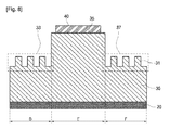
その後、図6に示すように、透明基板20上に形成されたレジン層30を、単位モールドパターン部10bが一つ以上形成されたマスターモールド(図5の10)で加圧するインプリント工程を行う。透明基板20及びレジン層30についての具体的な説明は、図1及び図2の説明で上述した通りであるので省略する。そして、光硬化工程又は熱硬化工程を経た後、マスターモールド(図5の10)をレジン層30から離型させると、図7に示すように、レジン層30上に単位モールドパターン部(図5及び図6の10b)と対応する単位パターン部30bを一つ以上形成することが可能である。ここで、単位パターン部30bは、第1のパターン領域33、第2のパターン領域37及び第1のパターン領域33と第2のパターン領域37の間に形成された突出パターン35からなり、第1のパターン領域33及び第2のパターン領域37は、複数の格子パターン31を備えることになる。
Thereafter, as shown in FIG. 6, an imprint process is performed in which the
ここで、突出パターン35の幅Eは、第1のパターン領域33の幅D又は第2のパターン領域37の幅Fよりも広く形成され、より具体的に突出パターン35の幅Eは、200〜1,000ナノメートルの範囲内で、第1のパターン領域33の幅D又は第2のパターン領域37の幅Fは、50〜100ナノメートルの範囲内で形成できるが、これらに限定されない。又、突出パターン35の高さは、格子パターン31の高さ以上に形成される。
Here, the width E of the protruding
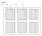
その後、格子パターン31及び突出パターン35上に金属を蒸着し、湿式エッチング工程を経て格子パターン31上に蒸着された金属を除去すると、図8に示すように、突出パターン35上にのみナノスケールを有する金属層40を形成でき、図9に示すような大面積を有する、ナノパターンを備えた透明基板を得ることができる。
Thereafter, a metal is deposited on the
10 マスターモールド
10b 単位モールドパターン部
11 格子モールドパターン
13 第1のモールドパターン領域
15 凹モールドパターン
17 第2のモールドパターン領域
20 透明基板
30 レジン層
30b 単位パターン部
31 格子パターン
33 第1のパターン領域
35 突出パターン
37 第2のパターン領域
40 金属層
DESCRIPTION OF SYMBOLS 10
Claims (1)
前記透明基板上に形成され、互いに対向する第1の表面および第2の表面を有する透明層と、
前記透明層の第2の表面に形成される第1のパターン領域及び第2のパターン領域と、
前記第1のパターン領域及び前記第2のパターン領域の間に形成されるように前記第2の表面から延びる第1の突出部と、
前記第1の突出部の上に形成される金属層と、
を含み、
前記第1の表面は、前記透明基板と向き合い、
前記第1及び第2のパターン領域のパターンは、複数の凹部によって形成され、
前記第1の突出部の高さは、前記第1及び第2のパターン領域のパターンの高さ以上であり、
前記第1のパターン領域または前記第2のパターン領域の互いに隣接する凹部の間に形成される凸部をさらに含み、
前記第1の突出部の幅は、前記凸部の幅以上であり、
前記第1の突出部と前記凸部は一体で形成され、
前記第1の突出部の幅は、前記第1のパターン領域の幅及び前記第2のパターン領域の幅のそれぞれよりも広い、タッチパネル用の導電性及び光透過性基板。 A transparent substrate;
A transparent layer formed on the transparent substrate and having a first surface and a second surface facing each other;
A first pattern region and a second pattern region formed on the second surface of the transparent layer;
A first protrusion extending from the second surface to be formed between the first pattern region and the second pattern region;
A metal layer formed on the first protrusion;
Including
The first surface faces the transparent substrate;
The pattern of the first and second pattern regions is formed by a plurality of recesses,
A height of the first protrusion is equal to or higher than a pattern height of the first and second pattern regions;
A convex portion formed between the concave portions adjacent to each other in the first pattern region or the second pattern region;
The width of the first protrusion is not less than the width of the protrusion ,
The first projecting portion and the convex portion are integrally formed,
The conductive and light-transmitting substrate for a touch panel, wherein the width of the first protrusion is wider than each of the width of the first pattern region and the width of the second pattern region.
Applications Claiming Priority (3)
| Application Number | Priority Date | Filing Date | Title |
|---|---|---|---|
| KR1020110137217A KR101856231B1 (en) | 2011-12-19 | 2011-12-19 | Transparent substrate with nano-pattern and method of manufacturing thereof |
| KR10-2011-0137217 | 2011-12-19 | ||
| PCT/KR2012/010739 WO2013094918A1 (en) | 2011-12-19 | 2012-12-11 | Transparent substrate having nano pattern and method of manufacturing the same |
Publications (3)
| Publication Number | Publication Date |
|---|---|
| JP2015503244A JP2015503244A (en) | 2015-01-29 |
| JP2015503244A5 JP2015503244A5 (en) | 2016-02-12 |
| JP6257522B2 true JP6257522B2 (en) | 2018-01-10 |
Family
ID=48668752
Family Applications (1)
| Application Number | Title | Priority Date | Filing Date |
|---|---|---|---|
| JP2014547095A Expired - Fee Related JP6257522B2 (en) | 2011-12-19 | 2012-12-11 | Conductive and light transmissive layer and method for producing the same |
Country Status (7)
| Country | Link |
|---|---|
| US (2) | US9536819B2 (en) |
| EP (1) | EP2795666B1 (en) |
| JP (1) | JP6257522B2 (en) |
| KR (1) | KR101856231B1 (en) |
| CN (1) | CN103503114B (en) |
| TW (1) | TW201340172A (en) |
| WO (1) | WO2013094918A1 (en) |
Families Citing this family (3)
| Publication number | Priority date | Publication date | Assignee | Title |
|---|---|---|---|---|
| KR101856231B1 (en) * | 2011-12-19 | 2018-05-10 | 엘지이노텍 주식회사 | Transparent substrate with nano-pattern and method of manufacturing thereof |
| WO2017126673A1 (en) * | 2016-01-22 | 2017-07-27 | Scivax株式会社 | Functional structural body |
| JP6958237B2 (en) * | 2017-10-30 | 2021-11-02 | セイコーエプソン株式会社 | Encoder scales, encoder scale manufacturing methods, encoders, robots, electronic component transfer devices, printers and projectors |
Family Cites Families (34)
| Publication number | Priority date | Publication date | Assignee | Title |
|---|---|---|---|---|
| JP2001075074A (en) | 1999-08-18 | 2001-03-23 | Internatl Business Mach Corp <Ibm> | Touch sensor type liquid crystal display device |
| JP2002341781A (en) * | 2001-05-16 | 2002-11-29 | Bridgestone Corp | Display panel |
| EP1388836A4 (en) | 2001-05-16 | 2006-05-03 | Bridgestone Corp | Electromagnetic wave shielding light-transmitting window member, its manufacturing method, and display panel |
| JP2003198186A (en) * | 2001-12-25 | 2003-07-11 | Dainippon Printing Co Ltd | Electromagnetic wave shielding sheet and method for manufacturing the same |
| JP4323219B2 (en) | 2002-05-31 | 2009-09-02 | 三星モバイルディスプレイ株式會社 | Surface light source device and liquid crystal display element assembly using the same |
| JP4262944B2 (en) * | 2002-08-08 | 2009-05-13 | アルプス電気株式会社 | Illumination device and liquid crystal display device |
| US7113249B2 (en) | 2003-01-06 | 2006-09-26 | Dai Nippon Printing Co., Ltd. | Monochrome liquid crystal display having higher spaces in pixel area than in peripheral area and production method therefor |
| JP4396459B2 (en) * | 2004-09-08 | 2010-01-13 | 日本ゼオン株式会社 | Electromagnetic wave shielding grid polarizer and manufacturing method thereof |
| KR20070041540A (en) | 2004-06-30 | 2007-04-18 | 니폰 제온 가부시키가이샤 | Electromagnetic wave shielding grid polarizer and its manufacturing method and grid polarizer manufacturing method |
| JP2007128091A (en) * | 2005-11-03 | 2007-05-24 | Samsung Electronics Co Ltd | Display substrate, method of manufacturing the same, and display panel having the same |
| KR101297234B1 (en) | 2006-09-26 | 2013-08-16 | 재단법인서울대학교산학협력재단 | Display substrate and method of manufacturing thereof |
| JP4336996B2 (en) * | 2006-10-03 | 2009-09-30 | セイコーエプソン株式会社 | Method for manufacturing plated substrate |
| JP4520445B2 (en) * | 2006-10-11 | 2010-08-04 | 旭化成イーマテリアルズ株式会社 | Wire grid polarizer |
| US7737392B2 (en) * | 2006-11-09 | 2010-06-15 | The Board Of Trustees Of The University Of Illinois | Photonic crystal sensors with integrated fluid containment structure, sample handling devices incorporating same, and uses thereof for biomolecular interaction analysis |
| JP2008126450A (en) * | 2006-11-17 | 2008-06-05 | Fuji Electric Device Technology Co Ltd | Mold, manufacturing method therefor and magnetic recording medium |
| JP2008181113A (en) | 2006-12-27 | 2008-08-07 | Toray Ind Inc | Reflection type polarizer and liquid crystal display device |
| EP1978407A1 (en) | 2007-03-28 | 2008-10-08 | CRF Societa'Consortile per Azioni | Method for obtaining a transparent conductive film |
| JP2008294372A (en) | 2007-05-28 | 2008-12-04 | Panasonic Corp | Electromagnetic wave shielding film |
| JP2009031392A (en) | 2007-07-25 | 2009-02-12 | Seiko Epson Corp | Wire-grid type polarizing element, method for manufacturing the same, liquid crystal device, and projection display device |
| WO2009041646A1 (en) * | 2007-09-28 | 2009-04-02 | Asahi Glass Company, Limited | Photocurable composition, method for producing fine patterned body, and optical device |
| WO2009148138A1 (en) | 2008-06-05 | 2009-12-10 | 旭硝子株式会社 | Mold for nanoimprinting, process for producing the same, and processes for producing molded resin having fine rugged structure on surface and for producing wire-grid polarizer |
| JP4766094B2 (en) | 2008-10-01 | 2011-09-07 | ソニー株式会社 | Display panel, display device |
| US20110187669A1 (en) | 2008-11-12 | 2011-08-04 | Sharp Kabushiki Kaisha | Liquid crystal display device and manufacting method thereof |
| JP2010205611A (en) | 2009-03-04 | 2010-09-16 | Casio Computer Co Ltd | Touch panel |
| KR101191981B1 (en) * | 2009-09-03 | 2012-10-17 | 한국표준과학연구원 | semiconductor nanowires array and manufacturing method thereof |
| WO2011065032A1 (en) * | 2009-11-27 | 2011-06-03 | 凸版印刷株式会社 | Transparent conductive laminate, method for producing same, and electrostatic capacitance type touch panel |
| US8493349B2 (en) | 2009-12-10 | 2013-07-23 | Lg Display Co., Ltd. | Touch screen panel |
| WO2011071096A1 (en) | 2009-12-11 | 2011-06-16 | 日本写真印刷株式会社 | Mounting structure for thin display and resistive touch panel, resistive touch panel unit with protrusions at front surface thereof, and thin display unit with protrusions at back surface thereof |
| JP5769734B2 (en) | 2010-02-05 | 2015-08-26 | モレキュラー・インプリンツ・インコーポレーテッド | Template with high contrast alignment mark |
| US8611077B2 (en) | 2010-08-27 | 2013-12-17 | Apple Inc. | Electronic devices with component mounting structures |
| KR20100129255A (en) | 2010-11-09 | 2010-12-08 | 최은석 | Display stand for electric mat |
| KR101197776B1 (en) | 2010-12-27 | 2012-11-06 | 엘지이노텍 주식회사 | method for manufacturing wire grid polarizer |
| US9557448B2 (en) | 2011-09-15 | 2017-01-31 | Soken Chemical & Engineering Co., Ltd. | Contact prevention film, touch panel and display device cover panel |
| KR101856231B1 (en) | 2011-12-19 | 2018-05-10 | 엘지이노텍 주식회사 | Transparent substrate with nano-pattern and method of manufacturing thereof |
-
2011
- 2011-12-19 KR KR1020110137217A patent/KR101856231B1/en active IP Right Grant
-
2012
- 2012-12-11 CN CN201280021740.2A patent/CN103503114B/en not_active Expired - Fee Related
- 2012-12-11 EP EP12860252.1A patent/EP2795666B1/en not_active Not-in-force
- 2012-12-11 JP JP2014547095A patent/JP6257522B2/en not_active Expired - Fee Related
- 2012-12-11 US US14/358,701 patent/US9536819B2/en not_active Expired - Fee Related
- 2012-12-11 WO PCT/KR2012/010739 patent/WO2013094918A1/en active Application Filing
- 2012-12-18 TW TW101148093A patent/TW201340172A/en unknown
-
2014
- 2014-10-03 US US14/506,406 patent/US20150022742A1/en not_active Abandoned
Also Published As
| Publication number | Publication date |
|---|---|
| KR20130070076A (en) | 2013-06-27 |
| US20150022742A1 (en) | 2015-01-22 |
| WO2013094918A1 (en) | 2013-06-27 |
| EP2795666A4 (en) | 2015-07-29 |
| US9536819B2 (en) | 2017-01-03 |
| CN103503114A (en) | 2014-01-08 |
| US20140272316A1 (en) | 2014-09-18 |
| EP2795666B1 (en) | 2019-06-12 |
| EP2795666A1 (en) | 2014-10-29 |
| CN103503114B (en) | 2017-05-03 |
| JP2015503244A (en) | 2015-01-29 |
| KR101856231B1 (en) | 2018-05-10 |
| TW201340172A (en) | 2013-10-01 |
Similar Documents
| Publication | Publication Date | Title |
|---|---|---|
| JP5437808B2 (en) | Method for patterning a material on a polymer substrate | |
| TWI584059B (en) | Method for manufacturing transparent photomask, transparent photomask manufactured by the method and method for manufacturing conductive mesh pattern using the transparent photomask | |
| JP5714731B2 (en) | Patterned flexible transparent conductive sheet and method for producing the same | |
| WO2017215388A1 (en) | Manufacturing method for electromagnetic shielding film and electromagnetic shielding window | |
| CN104698515A (en) | Method of making microarrays | |
| CN101116018A (en) | Method of patterning conductive layers, method of manufacturing polarizers, and polarizers manufactured using the same | |
| JP6257522B2 (en) | Conductive and light transmissive layer and method for producing the same | |
| EP2231508A2 (en) | Carbon nanotube patterning on a metal substrate | |
| CN106782741A (en) | A kind of flexible transparent conducting film based on nano impression and preparation method thereof | |
| JP2011248324A (en) | Conductive element and method of manufacturing the same, interconnection element, information input device, display device, and electronic apparatus | |
| US20100096770A1 (en) | Method for fabrication of mold for nano imprinting and method for production of photonic crystal using the same | |
| CN104966588A (en) | Method of preparing nano-level metal grid transparent conductive film | |
| EP3619160B1 (en) | Methods for micro and nano fabrication by selective template removal | |
| CN109407461B (en) | Photomask, method of manufacturing the same, and method of manufacturing display device | |
| US20130082029A1 (en) | Stamper, imprint device, product processed by imprint device, device for manufacturing product processed by imprint device, and method for manufacturing product processed by imprint device | |
| Chung et al. | Fabrication of metallic nanomesh structures using phase shift lithography and its application to touch screen panels | |
| KR20110002705A (en) | Forming method of fine pattern | |
| KR102361796B1 (en) | Method for manufacturing mold, and method for manufacturing electrode film and electrode film using thereof | |
| TW202102356A (en) | Device comprising physical properties controlled by microstructure and method of manufacturing the same | |
| US9520258B2 (en) | Selective synthesis of nanotubes without inhibitor | |
| TWI500979B (en) | Base nano-mold and method of manufacturing nano-mold using the same | |
| JP2011191766A (en) | Method for patterning conductive layer, method for manufacturing polarizing element using the same, and polarizing element manufactured by the method | |
| KR20050107118A (en) | Method for manufacturing mold for uv embossing | |
| KR101615092B1 (en) | Method of manufacturing patternen functional film | |
| JP2006118028A (en) | Method for selectively forming layer |
Legal Events
| Date | Code | Title | Description |
|---|---|---|---|
| A521 | Request for written amendment filed |
Free format text: JAPANESE INTERMEDIATE CODE: A523 Effective date: 20151211 |
|
| A621 | Written request for application examination |
Free format text: JAPANESE INTERMEDIATE CODE: A621 Effective date: 20151211 |
|
| A131 | Notification of reasons for refusal |
Free format text: JAPANESE INTERMEDIATE CODE: A131 Effective date: 20160913 |
|
| A521 | Request for written amendment filed |
Free format text: JAPANESE INTERMEDIATE CODE: A523 Effective date: 20161207 |
|
| A02 | Decision of refusal |
Free format text: JAPANESE INTERMEDIATE CODE: A02 Effective date: 20170214 |
|
| RD03 | Notification of appointment of power of attorney |
Free format text: JAPANESE INTERMEDIATE CODE: A7423 Effective date: 20170330 |
|
| RD13 | Notification of appointment of power of sub attorney |
Free format text: JAPANESE INTERMEDIATE CODE: A7433 Effective date: 20170602 |
|
| A521 | Request for written amendment filed |
Free format text: JAPANESE INTERMEDIATE CODE: A523 Effective date: 20170613 |
|
| A911 | Transfer to examiner for re-examination before appeal (zenchi) |
Free format text: JAPANESE INTERMEDIATE CODE: A911 Effective date: 20170821 |
|
| A131 | Notification of reasons for refusal |
Free format text: JAPANESE INTERMEDIATE CODE: A131 Effective date: 20170926 |
|
| A521 | Request for written amendment filed |
Free format text: JAPANESE INTERMEDIATE CODE: A523 Effective date: 20170929 |
|
| TRDD | Decision of grant or rejection written | ||
| A01 | Written decision to grant a patent or to grant a registration (utility model) |
Free format text: JAPANESE INTERMEDIATE CODE: A01 Effective date: 20171107 |
|
| A61 | First payment of annual fees (during grant procedure) |
Free format text: JAPANESE INTERMEDIATE CODE: A61 Effective date: 20171205 |
|
| R150 | Certificate of patent or registration of utility model |
Ref document number: 6257522 Country of ref document: JP Free format text: JAPANESE INTERMEDIATE CODE: R150 |
|
| LAPS | Cancellation because of no payment of annual fees |