JP6958237B2 - Encoder scales, encoder scale manufacturing methods, encoders, robots, electronic component transfer devices, printers and projectors - Google Patents
Encoder scales, encoder scale manufacturing methods, encoders, robots, electronic component transfer devices, printers and projectors Download PDFInfo
- Publication number
- JP6958237B2 JP6958237B2 JP2017209385A JP2017209385A JP6958237B2 JP 6958237 B2 JP6958237 B2 JP 6958237B2 JP 2017209385 A JP2017209385 A JP 2017209385A JP 2017209385 A JP2017209385 A JP 2017209385A JP 6958237 B2 JP6958237 B2 JP 6958237B2
- Authority
- JP
- Japan
- Prior art keywords
- encoder scale
- region
- encoder
- base material
- light
- Prior art date
- Legal status (The legal status is an assumption and is not a legal conclusion. Google has not performed a legal analysis and makes no representation as to the accuracy of the status listed.)
- Active
Links
- 238000004519 manufacturing process Methods 0.000 title claims description 14
- 239000000463 material Substances 0.000 claims description 98
- 239000011347 resin Substances 0.000 claims description 81
- 229920005989 resin Polymers 0.000 claims description 81
- 229910052751 metal Inorganic materials 0.000 claims description 41
- 239000002184 metal Substances 0.000 claims description 41
- 238000000034 method Methods 0.000 claims description 30
- 230000003287 optical effect Effects 0.000 claims description 26
- 238000005530 etching Methods 0.000 claims description 22
- 229910021421 monocrystalline silicon Inorganic materials 0.000 claims description 21
- 239000013078 crystal Substances 0.000 claims description 15
- 239000000758 substrate Substances 0.000 claims description 14
- 239000002178 crystalline material Substances 0.000 claims description 6
- 238000000059 patterning Methods 0.000 claims description 3
- 238000001514 detection method Methods 0.000 description 20
- 239000004973 liquid crystal related substance Substances 0.000 description 12
- 239000000470 constituent Substances 0.000 description 5
- 238000005520 cutting process Methods 0.000 description 5
- 239000007769 metal material Substances 0.000 description 5
- 239000011521 glass Substances 0.000 description 4
- 230000015572 biosynthetic process Effects 0.000 description 3
- 238000007689 inspection Methods 0.000 description 3
- 238000009434 installation Methods 0.000 description 3
- 238000011144 upstream manufacturing Methods 0.000 description 3
- XEEYBQQBJWHFJM-UHFFFAOYSA-N Iron Chemical compound [Fe] XEEYBQQBJWHFJM-UHFFFAOYSA-N 0.000 description 2
- PXHVJJICTQNCMI-UHFFFAOYSA-N Nickel Chemical compound [Ni] PXHVJJICTQNCMI-UHFFFAOYSA-N 0.000 description 2
- 206010034972 Photosensitivity reaction Diseases 0.000 description 2
- 239000000853 adhesive Substances 0.000 description 2
- 230000001070 adhesive effect Effects 0.000 description 2
- 229910052782 aluminium Inorganic materials 0.000 description 2
- XAGFODPZIPBFFR-UHFFFAOYSA-N aluminium Chemical compound [Al] XAGFODPZIPBFFR-UHFFFAOYSA-N 0.000 description 2
- 239000012636 effector Substances 0.000 description 2
- 230000007613 environmental effect Effects 0.000 description 2
- 238000009616 inductively coupled plasma Methods 0.000 description 2
- 238000001579 optical reflectometry Methods 0.000 description 2
- 238000000206 photolithography Methods 0.000 description 2
- 230000036211 photosensitivity Effects 0.000 description 2
- 238000001020 plasma etching Methods 0.000 description 2
- 238000005498 polishing Methods 0.000 description 2
- 238000002360 preparation method Methods 0.000 description 2
- 230000001681 protective effect Effects 0.000 description 2
- 239000004065 semiconductor Substances 0.000 description 2
- 239000000126 substance Substances 0.000 description 2
- WGTYBPLFGIVFAS-UHFFFAOYSA-M tetramethylammonium hydroxide Chemical compound [OH-].C[N+](C)(C)C WGTYBPLFGIVFAS-UHFFFAOYSA-M 0.000 description 2
- 239000012780 transparent material Substances 0.000 description 2
- 238000001039 wet etching Methods 0.000 description 2
- 238000009623 Bosch process Methods 0.000 description 1
- RYGMFSIKBFXOCR-UHFFFAOYSA-N Copper Chemical compound [Cu] RYGMFSIKBFXOCR-UHFFFAOYSA-N 0.000 description 1
- RTAQQCXQSZGOHL-UHFFFAOYSA-N Titanium Chemical compound [Ti] RTAQQCXQSZGOHL-UHFFFAOYSA-N 0.000 description 1
- 239000003522 acrylic cement Substances 0.000 description 1
- 230000001154 acute effect Effects 0.000 description 1
- 239000000654 additive Substances 0.000 description 1
- 229910045601 alloy Inorganic materials 0.000 description 1
- 239000000956 alloy Substances 0.000 description 1
- 238000003491 array Methods 0.000 description 1
- 238000011965 cell line development Methods 0.000 description 1
- 239000011248 coating agent Substances 0.000 description 1
- 238000000576 coating method Methods 0.000 description 1
- 239000002131 composite material Substances 0.000 description 1
- 229920001577 copolymer Polymers 0.000 description 1
- 229910052802 copper Inorganic materials 0.000 description 1
- 239000010949 copper Substances 0.000 description 1
- 238000007599 discharging Methods 0.000 description 1
- 238000001312 dry etching Methods 0.000 description 1
- 229920006332 epoxy adhesive Polymers 0.000 description 1
- 239000003822 epoxy resin Substances 0.000 description 1
- 239000000945 filler Substances 0.000 description 1
- 238000000227 grinding Methods 0.000 description 1
- 229910052742 iron Inorganic materials 0.000 description 1
- 230000031700 light absorption Effects 0.000 description 1
- 150000002739 metals Chemical class 0.000 description 1
- 229910052759 nickel Inorganic materials 0.000 description 1
- 230000000149 penetrating effect Effects 0.000 description 1
- 230000000737 periodic effect Effects 0.000 description 1
- 239000000049 pigment Substances 0.000 description 1
- 229920000647 polyepoxide Polymers 0.000 description 1
- 229920001721 polyimide Polymers 0.000 description 1
- 239000009719 polyimide resin Substances 0.000 description 1
- 239000010453 quartz Substances 0.000 description 1
- 238000007788 roughening Methods 0.000 description 1
- HBMJWWWQQXIZIP-UHFFFAOYSA-N silicon carbide Chemical compound [Si+]#[C-] HBMJWWWQQXIZIP-UHFFFAOYSA-N 0.000 description 1
- 229910010271 silicon carbide Inorganic materials 0.000 description 1
- VYPSYNLAJGMNEJ-UHFFFAOYSA-N silicon dioxide Inorganic materials O=[Si]=O VYPSYNLAJGMNEJ-UHFFFAOYSA-N 0.000 description 1
- 238000004544 sputter deposition Methods 0.000 description 1
- 239000010935 stainless steel Substances 0.000 description 1
- 229910001220 stainless steel Inorganic materials 0.000 description 1
- 239000010936 titanium Substances 0.000 description 1
- 229910052719 titanium Inorganic materials 0.000 description 1
- WFKWXMTUELFFGS-UHFFFAOYSA-N tungsten Chemical compound [W] WFKWXMTUELFFGS-UHFFFAOYSA-N 0.000 description 1
- 229910052721 tungsten Inorganic materials 0.000 description 1
- 239000010937 tungsten Substances 0.000 description 1
- 235000012431 wafers Nutrition 0.000 description 1
Images


Classifications
-
- G—PHYSICS
- G01—MEASURING; TESTING
- G01D—MEASURING NOT SPECIALLY ADAPTED FOR A SPECIFIC VARIABLE; ARRANGEMENTS FOR MEASURING TWO OR MORE VARIABLES NOT COVERED IN A SINGLE OTHER SUBCLASS; TARIFF METERING APPARATUS; MEASURING OR TESTING NOT OTHERWISE PROVIDED FOR
- G01D5/00—Mechanical means for transferring the output of a sensing member; Means for converting the output of a sensing member to another variable where the form or nature of the sensing member does not constrain the means for converting; Transducers not specially adapted for a specific variable
- G01D5/26—Mechanical means for transferring the output of a sensing member; Means for converting the output of a sensing member to another variable where the form or nature of the sensing member does not constrain the means for converting; Transducers not specially adapted for a specific variable characterised by optical transfer means, i.e. using infrared, visible, or ultraviolet light
- G01D5/32—Mechanical means for transferring the output of a sensing member; Means for converting the output of a sensing member to another variable where the form or nature of the sensing member does not constrain the means for converting; Transducers not specially adapted for a specific variable characterised by optical transfer means, i.e. using infrared, visible, or ultraviolet light with attenuation or whole or partial obturation of beams of light
- G01D5/34—Mechanical means for transferring the output of a sensing member; Means for converting the output of a sensing member to another variable where the form or nature of the sensing member does not constrain the means for converting; Transducers not specially adapted for a specific variable characterised by optical transfer means, i.e. using infrared, visible, or ultraviolet light with attenuation or whole or partial obturation of beams of light the beams of light being detected by photocells
- G01D5/347—Mechanical means for transferring the output of a sensing member; Means for converting the output of a sensing member to another variable where the form or nature of the sensing member does not constrain the means for converting; Transducers not specially adapted for a specific variable characterised by optical transfer means, i.e. using infrared, visible, or ultraviolet light with attenuation or whole or partial obturation of beams of light the beams of light being detected by photocells using displacement encoding scales
- G01D5/34707—Scales; Discs, e.g. fixation, fabrication, compensation
-
- G—PHYSICS
- G01—MEASURING; TESTING
- G01D—MEASURING NOT SPECIALLY ADAPTED FOR A SPECIFIC VARIABLE; ARRANGEMENTS FOR MEASURING TWO OR MORE VARIABLES NOT COVERED IN A SINGLE OTHER SUBCLASS; TARIFF METERING APPARATUS; MEASURING OR TESTING NOT OTHERWISE PROVIDED FOR
- G01D5/00—Mechanical means for transferring the output of a sensing member; Means for converting the output of a sensing member to another variable where the form or nature of the sensing member does not constrain the means for converting; Transducers not specially adapted for a specific variable
- G01D5/26—Mechanical means for transferring the output of a sensing member; Means for converting the output of a sensing member to another variable where the form or nature of the sensing member does not constrain the means for converting; Transducers not specially adapted for a specific variable characterised by optical transfer means, i.e. using infrared, visible, or ultraviolet light
- G01D5/32—Mechanical means for transferring the output of a sensing member; Means for converting the output of a sensing member to another variable where the form or nature of the sensing member does not constrain the means for converting; Transducers not specially adapted for a specific variable characterised by optical transfer means, i.e. using infrared, visible, or ultraviolet light with attenuation or whole or partial obturation of beams of light
- G01D5/34—Mechanical means for transferring the output of a sensing member; Means for converting the output of a sensing member to another variable where the form or nature of the sensing member does not constrain the means for converting; Transducers not specially adapted for a specific variable characterised by optical transfer means, i.e. using infrared, visible, or ultraviolet light with attenuation or whole or partial obturation of beams of light the beams of light being detected by photocells
- G01D5/353—Mechanical means for transferring the output of a sensing member; Means for converting the output of a sensing member to another variable where the form or nature of the sensing member does not constrain the means for converting; Transducers not specially adapted for a specific variable characterised by optical transfer means, i.e. using infrared, visible, or ultraviolet light with attenuation or whole or partial obturation of beams of light the beams of light being detected by photocells influencing the transmission properties of an optical fibre
- G01D5/35338—Mechanical means for transferring the output of a sensing member; Means for converting the output of a sensing member to another variable where the form or nature of the sensing member does not constrain the means for converting; Transducers not specially adapted for a specific variable characterised by optical transfer means, i.e. using infrared, visible, or ultraviolet light with attenuation or whole or partial obturation of beams of light the beams of light being detected by photocells influencing the transmission properties of an optical fibre using other arrangements than interferometer arrangements
- G01D5/35354—Sensor working in reflection
-
- G—PHYSICS
- G01—MEASURING; TESTING
- G01D—MEASURING NOT SPECIALLY ADAPTED FOR A SPECIFIC VARIABLE; ARRANGEMENTS FOR MEASURING TWO OR MORE VARIABLES NOT COVERED IN A SINGLE OTHER SUBCLASS; TARIFF METERING APPARATUS; MEASURING OR TESTING NOT OTHERWISE PROVIDED FOR
- G01D5/00—Mechanical means for transferring the output of a sensing member; Means for converting the output of a sensing member to another variable where the form or nature of the sensing member does not constrain the means for converting; Transducers not specially adapted for a specific variable
- G01D5/26—Mechanical means for transferring the output of a sensing member; Means for converting the output of a sensing member to another variable where the form or nature of the sensing member does not constrain the means for converting; Transducers not specially adapted for a specific variable characterised by optical transfer means, i.e. using infrared, visible, or ultraviolet light
- G01D5/32—Mechanical means for transferring the output of a sensing member; Means for converting the output of a sensing member to another variable where the form or nature of the sensing member does not constrain the means for converting; Transducers not specially adapted for a specific variable characterised by optical transfer means, i.e. using infrared, visible, or ultraviolet light with attenuation or whole or partial obturation of beams of light
- G01D5/34—Mechanical means for transferring the output of a sensing member; Means for converting the output of a sensing member to another variable where the form or nature of the sensing member does not constrain the means for converting; Transducers not specially adapted for a specific variable characterised by optical transfer means, i.e. using infrared, visible, or ultraviolet light with attenuation or whole or partial obturation of beams of light the beams of light being detected by photocells
- G01D5/36—Forming the light into pulses
- G01D5/366—Particular pulse shapes
Description
本発明は、エンコーダースケール、エンコーダースケールの製造方法、エンコーダー、ロボット、電子部品搬送装置、プリンターおよびプロジェクターに関する。 The present invention relates to an encoder scale, a method for manufacturing an encoder scale, an encoder, a robot, an electronic component transfer device, a printer and a projector.
エンコーダーの一種として光学式のエンコーダーが知られている。例えば、特許文献1に記載の反射型光学式エンコーダーは、光源および光検出器と、光源および光検出器に対して相対的に移動する光学パターンを有するスケールと、を備え、光源がスケールに向けて光ビームを射出し、光検出器がスケールによって反射・変調された光ビームを検出する。ここで、特許文献1に記載のスケールは、ガラス基板と、ガラス基板の表面に形成された周期的な光学パターンと、を有し、光学パターンが、スケールの移動方向に一次元配列された複数の金属薄膜からなる。
An optical encoder is known as a kind of encoder. For example, the reflective optical encoder described in
特許文献1に記載のスケールは、基材としてガラス基板を用いるため、形状の自由度が低く、また、低コスト化が難しいという課題がある。また、特許文献1に記載のスケールは、ガラス基板の金属膜の形成されていない部分の面が金属膜の面と同一方向に沿っているため、当該部分で透過せずに反射した光ビームの一部が光検出器で検出されてしまい、その結果、検出精度を高めることが難しいという課題もある。
Since the scale described in
本発明の目的は、低コスト化を図りつつ、検出精度を高めることができるエンコーダースケールおよびその製造方法を提供すること、また、このエンコーダースケールを備えるエンコーダー、ロボット、電子部品搬送装置、プリンターおよびプロジェクターを提供することにある。 An object of the present invention is to provide an encoder scale and a method for manufacturing the same, which can improve the detection accuracy while reducing the cost, and an encoder, a robot, an electronic component transfer device, a printer and a projector provided with the encoder scale. Is to provide.
本発明は、上述の課題の少なくとも一部を解決するためになされたものであり、以下の適用例または形態として実現することが可能である。 The present invention has been made to solve at least a part of the above-mentioned problems, and can be realized as the following application examples or forms.
本適用例のエンコーダースケールは、板状の基材と、
前記基材の一方の面に設けられ、第1領域と第2領域とが交互に並んでいる光学パターンと、を備え、
前記第1領域は、
前記基材上にパターニングされて配置され、感光性樹脂を含む樹脂層と、
前記樹脂層上に配置された金属膜と、を有し、
前記第1領域の表面は、前記基材の厚さ方向を法線とする第1面を主体に構成され、
前記第2領域の表面は、前記第1面に対して傾斜している第2面を主体に構成されていることを特徴とする。
The encoder scale of this application example is a plate-shaped base material and
An optical pattern provided on one surface of the base material and in which a first region and a second region are alternately arranged is provided.
The first region is
A resin layer patterned and arranged on the substrate and containing a photosensitive resin,
It has a metal film arranged on the resin layer and
The surface of the first region is mainly composed of the first surface having the thickness direction of the base material as a normal.
The surface of the second region is mainly composed of a second surface that is inclined with respect to the first surface.
このようなエンコーダースケールによれば、第1領域の表面が基材の厚さ方向を法線とする第1面を主体に構成され、第2領域の表面が第1面に対して傾斜している第2面を主体に構成されているため、第1領域および第2領域で反射した光の方向を互いに異ならせ、第1領域で反射した光のみを選択的に受光することができる。そのため、基材を透明材料で構成する必要がなく、基材の材料選択の自由度を高めることができ、その結果、より安価でかつ加工性に優れた材料を用いることができる。また、第1領域に光が照射されている状態とそうでない状態との受光量の差を大きくすることができ、その結果、検出精度を高めることができる。 According to such an encoder scale, the surface of the first region is mainly composed of the first surface whose normal is the thickness direction of the base material, and the surface of the second region is inclined with respect to the first surface. Since it is mainly composed of the second surface, the directions of the light reflected in the first region and the second region are different from each other, and only the light reflected in the first region can be selectively received. Therefore, it is not necessary to compose the base material with a transparent material, and the degree of freedom in selecting the material of the base material can be increased, and as a result, a material that is cheaper and has excellent workability can be used. Further, the difference in the amount of received light between the state where the first region is irradiated with light and the state where it is not irradiated can be increased, and as a result, the detection accuracy can be improved.
また、第1領域が有する樹脂層が、基材上にパターニングされて配置され、感光性樹脂を含んで構成されているため、フォトリソグラフィ法を用いて第1領域を高精度に形成することができる。そして、第1領域が有する金属膜が、樹脂層上に配置され、金属材料で構成されているため、第1領域の光反射性を高めることができる。このように、第1領域が樹脂層および金属膜を有することにより、この点でも、検出精度を高めることができる。 Further, since the resin layer of the first region is patterned and arranged on the base material and is composed of the photosensitive resin, the first region can be formed with high accuracy by using a photolithography method. can. Since the metal film of the first region is arranged on the resin layer and is made of a metal material, the light reflectivity of the first region can be enhanced. As described above, since the first region has the resin layer and the metal film, the detection accuracy can be improved in this respect as well.
本適用例のエンコーダースケールでは、前記基材は、異方性エッチングが可能な結晶材料で構成されていることが好ましい。
これにより、結晶材料の結晶面を利用して第2領域の第2面を形成することができる。
In the encoder scale of this application example, it is preferable that the base material is made of a crystalline material capable of anisotropic etching.
Thereby, the crystal plane of the crystal material can be used to form the second plane of the second region.
本適用例のエンコーダースケールでは、前記結晶材料は、単結晶シリコンであることが好ましい。 In the encoder scale of this application example, the crystal material is preferably single crystal silicon.
単結晶シリコンは、他の結晶材料に比べて安価であり、高精度な加工が容易である。そのため、エンコーダースケールの基材が単結晶シリコンで構成されていることで、エンコーダースケールの低コスト化および高精度化が容易に図れるという利点がある。 Single crystal silicon is cheaper than other crystalline materials and is easy to process with high precision. Therefore, since the base material of the encoder scale is made of single crystal silicon, there is an advantage that the cost and accuracy of the encoder scale can be easily reduced.
本適用例のエンコーダースケールでは、前記単結晶シリコンの面方位が(100)であることが好ましい。 In the encoder scale of this application example, the plane orientation of the single crystal silicon is preferably (100).
これにより、[100]面を使用することで、第2領域122に形成される構造体を正四角錘とすることができる。そのため、このような単結晶シリコンを用いることで、リニアエンコーダーだけでなく、ロータリーエンコーダーに適したエンコーダースケールを形成することができる。
Thereby, by using the [100] plane, the structure formed in the
本適用例のエンコーダースケールでは、前記第2面は、前記結晶材料の結晶面に沿って設けられていることが好ましい。 In the encoder scale of this application example, it is preferable that the second surface is provided along the crystal plane of the crystal material.
これにより、第1面に対する傾斜角度のバラつきの少ない第2面を容易に形成することができる。 As a result, it is possible to easily form the second surface with little variation in the inclination angle with respect to the first surface.
本適用例のエンコーダースケールでは、前記感光性樹脂は、ネガ型であることが好ましい。 In the encoder scale of this application example, the photosensitive resin is preferably a negative type.
これにより、感光性樹脂がポジ型である場合に比べて、高精度な第1領域の形成が容易となる。 As a result, it becomes easier to form the first region with high accuracy as compared with the case where the photosensitive resin is of the positive type.
本適用例のエンコーダースケールの製造方法は、板状の基材の一方の面に、異方性エッチングを行って、前記基材の厚さ方向を法線とする面に対して傾斜している面を主体に構成されている第1領域を形成する工程と、
前記一方の面上に、感光性樹脂を塗布し、パターニングすることにより樹脂層を形成した後に、前記樹脂層上に金属膜を成膜することにより、前記基材の厚さ方向を法線とする面を主体に構成されている第2領域を形成する工程と、を含むことを特徴とする。
In the method for manufacturing an encoder scale of this application example, one surface of a plate-shaped base material is anisotropically etched to be inclined with respect to a surface whose normal is the thickness direction of the base material. The process of forming the first region, which is mainly composed of surfaces, and
A photosensitive resin is applied onto one of the surfaces to form a resin layer by patterning, and then a metal film is formed on the resin layer so that the thickness direction of the base material becomes a normal. It is characterized by including a step of forming a second region mainly composed of a surface to be formed.
このようなエンコーダースケールの製造方法によれば、低コスト化を図りつつ、検出精度を高めることができるエンコーダースケールを得ることができる。 According to such an encoder scale manufacturing method, it is possible to obtain an encoder scale capable of improving the detection accuracy while reducing the cost.
本適用例のエンコーダーは、本適用例のエンコーダースケールと、
前記エンコーダースケールに向けて光を出射する光出射部と、
前記エンコーダースケールで反射した前記光を検出する光検出部と、を備えることを特徴とする。
The encoder of this application example is the encoder scale of this application example.
A light emitting unit that emits light toward the encoder scale,
It is characterized by including a photodetector for detecting the light reflected by the encoder scale.
このようなエンコーダーによれば、低コスト化を図りつつ、検出精度を高めることができる。 According to such an encoder, it is possible to improve the detection accuracy while reducing the cost.
本適用例のロボットは、本適用例のエンコーダースケールを備えることを特徴とする。
このようなロボットによれば、エンコーダースケールの低コスト化を図ることで、ロボットの低コスト化を図ることができる。また、エンコーダースケールを用いた高精度な検出結果に基づいて高精度な動作制御を行うことができる。
The robot of this application example is characterized by including the encoder scale of this application example.
According to such a robot, the cost of the robot can be reduced by reducing the cost of the encoder scale. In addition, highly accurate operation control can be performed based on a highly accurate detection result using the encoder scale.
本適用例の電子部品搬送装置は、本適用例のエンコーダースケールを備えることを特徴とする。 The electronic component transfer device of this application example is characterized by including the encoder scale of this application example.
このような電子部品搬送装置によれば、エンコーダースケールの低コスト化を図ることで、電子部品搬送装置の低コスト化を図ることができる。また、エンコーダースケールを用いた高精度な検出結果に基づいて高精度な動作制御を行うことができる。 According to such an electronic component transfer device, the cost of the electronic component transfer device can be reduced by reducing the cost of the encoder scale. In addition, highly accurate operation control can be performed based on a highly accurate detection result using the encoder scale.
本適用例のプリンターは、本適用例のエンコーダースケールを備えることを特徴とする。 The printer of this application example is characterized by including the encoder scale of this application example.
このようなプリンターによれば、エンコーダースケールの低コスト化を図ることで、プリンターの低コスト化を図ることができる。また、エンコーダースケールを用いた高精度な検出結果に基づいて高精度な動作制御を行うことができる。 According to such a printer, the cost of the printer can be reduced by reducing the cost of the encoder scale. In addition, highly accurate operation control can be performed based on a highly accurate detection result using the encoder scale.
本適用例のプロジェクターは、本適用例のエンコーダースケールを備えることを特徴とする。 The projector of this application example is characterized by including the encoder scale of this application example.
このようなプロジェクターによれば、エンコーダースケールの低コスト化を図ることで、プロジェクターの低コスト化を図ることができる。また、エンコーダースケールを用いた高精度な検出結果に基づいて高精度な動作制御を行うことができる。 According to such a projector, the cost of the projector can be reduced by reducing the cost of the encoder scale. In addition, highly accurate operation control can be performed based on a highly accurate detection result using the encoder scale.
以下、本発明のエンコーダースケール、エンコーダースケールの製造方法、エンコーダー、ロボット、電子部品搬送装置、プリンターおよびプロジェクターを添付図面に示す好適な実施形態に基づいて詳細に説明する。 Hereinafter, the encoder scale, the method for manufacturing the encoder scale, the encoder, the robot, the electronic component transfer device, the printer, and the projector of the present invention will be described in detail based on the preferred embodiments shown in the accompanying drawings.
(エンコーダー)
まず、本発明のエンコーダースケールの説明に先立ち、本発明のエンコーダー(本発明のエンコーダースケールを備えるエンコーダー)について簡単に説明する。
(encoder)
First, prior to the description of the encoder scale of the present invention, the encoder of the present invention (encoder including the encoder scale of the present invention) will be briefly described.
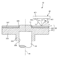
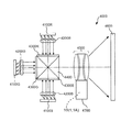
図1は、本発明の第1実施形態に係るエンコーダーを示す縦断面図である。図2は、図1に示すエンコーダーが備えるエンコーダースケールユニットの平面図である。なお、以下では、説明の便宜上、図1中の上側を「上」、下側を「下」という。 FIG. 1 is a vertical cross-sectional view showing an encoder according to the first embodiment of the present invention. FIG. 2 is a plan view of an encoder scale unit included in the encoder shown in FIG. In the following, for convenience of explanation, the upper side in FIG. 1 is referred to as “upper” and the lower side is referred to as “lower”.
図1に示すエンコーダー10は、図示しないモーター等が有する回転軸20の端部に固定されているエンコーダースケールユニット30と、エンコーダースケールユニット30の回転状態を検出する光学センサー40と、を有する。
The
エンコーダースケールユニット30は、回転軸20に固定されているハブ301と、ハブ301の支持部303にエポキシ系接着剤、アクリル系接着剤等の接着剤302により接着されているエンコーダースケール1と、を有する。
The
ハブ301は、円板状をなしている支持部303と、支持部303の一方(図1中下側)の面(下面)から突出している突出部304と、支持部303の他方(図1中上側)の面(上面)から突出している凸部305と、突出部304の先端面(図1中下側の面)に開口している凹部306と、を有し、これらが軸線axを中心として同軸的に設けられている。ここで、凹部306には、回転軸20の端部が挿入(例えば圧入)された状態で固定されている。このようなハブ301の構成材料としては、特に限定されないが、例えば、アルミニウム、ステンレス鋼等の金属材料が挙げられる。なお、凹部306に代えて、回転軸20が挿入される貫通孔をハブ301に設けてもよい。また、ハブ301は、回転軸20と一体で構成されていてもよい。
The
支持部303の上面は、エンコーダースケール1が設置される設置面307である。この支持部303の上面(設置面307)には、エンコーダースケール1の面内方向での位置決めを行うための位置決め部として機能する凸部305が設けられている。本実施形態では、凸部305の外形は、図2に示すように、軸線axに沿った方向から見たとき(以下、「平面視」ともいう)、円形をなしている。この凸部305は、その中心軸が軸線ax(回転軸20の中心軸)に一致するように形成されている。なお、凸部305の平面視での外形は、円形に限定されず、例えば、四角形、五角形等の多角形でもよい。
The upper surface of the
エンコーダースケール1は、板状(円板状)をなしており、その中央部には、厚さ方向(図1中上下方向)に貫通している孔11が形成されている。この孔11には、前述した凸部305が挿通されている。本実施形態では、孔11は、図2に示すように、平面視で円形をなしている。ここで、凸部305の直径(常温)は、孔11の直径(常温)より小さく設定されている。なお、孔11の平面視での外形は、円形に限定されず、例えば、四角形、五角形等の多角形でもよく、また、前述した凸部305の平面視の外形と異なっていてもよい。
The
また、エンコーダースケール1の上面には、図2に示すように、エンコーダースケール1の回転量(角度)、回転速度等を検出し得るパターンとして、軸線axを中心とする周方向に沿って光LLの反射方向の異なる第1領域121および第2領域122を周方向に沿って交互に並べた光学パターン12が形成されている。ここで、第1領域121および第2領域122は、互いに異なる方向を法線とする面で構成されている。なお、エンコーダースケール1については、後に詳述する。
Further, as shown in FIG. 2, on the upper surface of the
光学センサー40は、エンコーダースケールユニット30のエンコーダースケール1に向けて光LLを出射するレーザダイオード、発光ダイオード等の発光素子を含む光源部402と、エンコーダースケール1からの光LL(反射光)を受光するフォトダイオード等の受光素子を含む受光部403と、を有し、これらが基板401に搭載されている。
The
このような光学センサー40は、エンコーダースケール1の上面(照射面)に前述した光学パターン12が形成されているため、エンコーダースケール1の軸線axまわりの回転に伴って、光学パターン12で反射した光LLが受光部403に入射する状態(図1中実線で示す光LLの状態)とそうでない状態(図1中破線で示す光LLの状態)とを交互に繰り返す。そのため、受光部403からの出力信号(電流値)の波形は、エンコーダースケール1の軸線axまわりの回転に伴って変化する。このような受光部403からの出力信号に基づいて、エンコーダースケール1の回転状態(回転角度や回転速度等)を検出することができる。
In such an
ここで、図示しないが、受光部403は、軸線axを中心とする周方向での異なる位置に設けられている2つの受光素子を有し、一方の受光素子がA相信号を出力し、他方の受光素子がA相信号とは位相が45°ずれたB相信号を出力する。なお、光源部402は、受光部403が有する2つの受光素子に対応する2つの発光素子を有していてもよいし、当該2つの受光素子に対応するようにスリット板等を用いて1つの発光素子からの光を分割してもよい。また、光源部402および受光部403は、それぞれ、レンズ等の光学素子を有していてもよい。
Here, although not shown, the
以上、エンコーダー10について簡単に説明した。以下、エンコーダースケール1について詳述する。
The
(エンコーダースケール)
図3は、図2中A−A線断面図(エンコーダースケールの断面図)である。図4は、図3に示す第2領域の一部(複数の凸部)を示す斜視図である。図5は、図3に示す第2領域に設けられている凸部(第2面)の平面図である。図6は、エンコーダースケールの一部の断面を示すSEM写真である。図7は、エンコーダースケールの一部の表面状態を示すSEM写真である。図8は、第2領域の光反射特性(回転角度と受光部での受光量との関係)を示すグラフである。なお、以下では、図3中上側を「上」、下側を「下」という。
(Encoder scale)
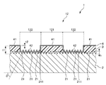
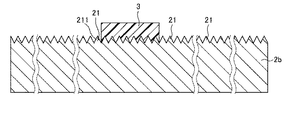
FIG. 3 is a cross-sectional view taken along the line AA in FIG. 2 (cross-sectional view of the encoder scale). FIG. 4 is a perspective view showing a part (plurality of convex portions) of the second region shown in FIG. FIG. 5 is a plan view of a convex portion (second surface) provided in the second region shown in FIG. FIG. 6 is an SEM photograph showing a cross section of a part of the encoder scale. FIG. 7 is an SEM photograph showing the surface state of a part of the encoder scale. FIG. 8 is a graph showing the light reflection characteristics (relationship between the rotation angle and the amount of light received by the light receiving portion) in the second region. In the following, the upper side in FIG. 3 is referred to as "upper" and the lower side is referred to as "lower".
前述したように、エンコーダースケール1の上面には、軸線axを中心とする周方向に沿って光LLの反射方向の異なる第1領域121および第2領域122を基材2の周方向に沿って交互に並べた光学パターン12が形成されている。この光学パターン12の第1領域121および第2領域122は、それぞれ、エンコーダースケール1の半径方向に沿って帯状に延びている。図2では、第1領域121および第2領域122が軸線axを中心として周方向に並んでいる領域において、平面視で第1領域121および第2領域122が互いに等しい形状となるように、第1領域121および第2領域122のそれぞれの幅がエンコーダースケール1の半径方向での内側から外側に向けて大きくなっている。なお、第1領域121および第2領域122の平面視形状は、図2に示す形状に限定されず、例えば、平面視で第1領域121または第2領域122の幅がエンコーダースケール1の半径方向にわたって一定となっていてもよい。
As described above, on the upper surface of the
ここで、エンコーダースケール1は、板状(円板状)の基材2と、基材2の上面上にパターニングされて設けられている樹脂層3と、これらを覆うように設けられている金属膜4と、を有し、平面視で樹脂層3が設けられている領域が第1領域121を構成し、平面視で第1領域121同士の間であって樹脂層3が設けられていない領域が第2領域122を構成している。したがって、金属膜4の樹脂層3と重なる部分の上面が第1領域121の表面であって反射面41を構成している。また、金属膜4の樹脂層3と重ならない部分の上面が第2領域122の表面であって反射面42を構成している。
Here, the
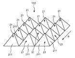
基材2の一方(図3中上側)の面には、複数の凸部21が設けられている。各凸部21は、図4に示すように、ピラミッド状(四角すい状)をなしており、基材2の板面に対して傾斜角度θで傾斜した4つの傾斜面211を有する。この傾斜角度θは、金属膜4の反射面42が反射面41と異なる方向に光LLを反射することができればよく、特に限定されないが、例えば、後述するように基材2を単結晶シリコンで構成した場合、約55°(理論値)である。なお、本実施形態では、複数の凸部21は、基材2の一方の面の全域にわたって配置されているが、これに限定されず、例えば、樹脂層3の直下の領域では凸部21を省略してもよい。ただし、複数の凸部21を基材2の一方の面の全域にわたって配置することで、複数の凸部21を形成する際、その形成領域の位置決め等が不要となり、簡便であるという利点がある。
A plurality of
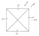
また、図示では、複数の凸部22は、互いに大きさが等しく、かつ、規則的に配置されているが、互いに大きさが異なっていてもよく、また、ランダムに配置されていてもよい。また、各凸部22は、図5に示すように平面視で四角形をなしており、複数の凸部22は、平面視での向きが揃っている。ここで、複数の凸部22は、平面視で、いかなる方向を向いていてもよいが、本実施形態では、複数の第2領域122間で互いに同じ方向を向いている。したがって、ある第2領域122に設けられている凸部22の平面視での各辺が当該ある第2領域122の延在方向Bに対して平行または直交である場合、当該ある第2領域122に対して軸線axまわりに55°異なる他の第2領域122に設けられている凸部22の平面視での各辺が当該他の第2領域122の延在方向Cに対して55°傾斜している。
Further, in the illustration, the plurality of convex portions 22 have the same size and are regularly arranged, but they may be different in size from each other or may be randomly arranged. Further, each convex portion 22 has a quadrangular shape in a plan view as shown in FIG. 5, and the plurality of convex portions 22 have the same orientation in a plan view. Here, the plurality of convex portions 22 may face in any direction in a plan view, but in the present embodiment, the plurality of
このような基材2は、いかなる材料で構成されていてもよいが、単結晶シリコン、シリコンカーバイト、水晶等の異方性エッチングが可能な結晶材料で構成されていることが好ましい。これにより、前述したような傾斜面211を簡単かつ高精度に形成することができる。そして、結晶材料の結晶面である傾斜面211を利用して第2領域122の反射面42(第2面)を形成することができる。
Such a
また、基材2に用いる結晶材料は、単結晶シリコンであることが好ましい。単結晶シリコンは、他の結晶材料に比べて安価であり、高精度な加工が容易である。そのため、エンコーダースケール1の基材2が単結晶シリコンで構成されていることで、エンコーダースケール1の低コスト化および高精度化が容易に図れるという利点がある。
Further, the crystal material used for the
特に、基材2に用いる単結晶シリコンの面方位は、(100)であることが好ましい。これにより、[100]面を使用することで、第2領域122に形成される構造体を正四角錘とすることができる。そのため、このような単結晶シリコンを用いることで、リニアエンコーダーだけでなく、本実施形態のようにロータリーエンコーダーに適したエンコーダースケール1を形成することができる。このように単結晶シリコンを用いて形成したエンコーダースケール1のSEM写真を図6および図7に示す。また、単結晶シリコンを用いて形成したエンコーダースケール1の第2領域122で反射して受光部403で受光される光LLの量は、図8に示すように、光源部402からの光LLの光量に対して3%以下とすることができる。
In particular, the plane orientation of the single crystal silicon used for the
このように基材2が異方性エッチング可能な結晶材料で構成されている場合、金属膜4の反射面42(第2面)は、基材2に用いる結晶材料の結晶面(傾斜面211)に沿って設けられていることが好ましい。これにより、反射面41(第1面)に対する傾斜角度θのバラつきの少ない反射面42(第2面)を容易に形成することができる。
When the
樹脂層3は、基材2の一方(図3中上側)の面上に配置されている。本実施形態では、前述したように基材2の一方の面の全域にわたって複数の凸部21が配置されているため、樹脂層3の直下には、複数の凸部21がある。この樹脂層3は、平面視で第1領域121の形状に対応した形状をなしている。また、樹脂層3の上面は、基材2の板面に沿った平坦面となっている。なお、図3に示す断面において、樹脂層3の側面は、樹脂層3の上面に対して直交しているが、樹脂層3の上面に対して傾斜していてもよく、その場合、反射面41の幅を規定しやすいという観点から、樹脂層3の幅が基材2側に向けて小さくなるように側面が形成されていることが好ましい。
The
このような樹脂層3は、感光性樹脂を用いて構成されている。かかる感光性樹脂としては、特に限定されず、例えば、感光性を有するポリイミド樹脂、エポキシ樹脂またはこれらのコポリマー等が挙げられる。また、かかる感光性樹脂は、ポジ型またはネガ型のいずれでもよいが、樹脂層3の上面と側面とからなる角部を直角または鋭角することで反射面41の寸法精度を高くすることができるという観点と環境信頼性の観点から、ネガ型であることが好ましい。このように、かかる感光性樹脂がネガ型であることで、感光性樹脂がポジ型である場合に比べて、高精度な第1領域121の形成が容易となる。なお、樹脂層3の構成材料には、前述した感光性樹脂以外の材料、例えば、フィラー、顔料、各種添加剤等が含まれていてもよい。
Such a
また、樹脂層3の厚さt1は、前述した凸部21の高さhよりも大きいことが好ましい。これにより、樹脂層3の直下に複数の凸部21が設けられていても、反射面41の平坦性を高めることができる。特に、樹脂層3の厚さt1および凸部21の高さhの比t1/hは、2以上12以下であることが好ましく、2以上10以下であることがより好ましく、2以上4以下であることがさらに好ましい。これにより、基材2上に樹脂層3を形成する際、複数の凸部21上に樹脂層3を形成する場合であっても、当該複数の凸部21の形状の影響を受け難くすることができ、CMP(chemical mechanical polishing)等の平坦化処理を行わなくても、平坦な表面を有する樹脂層3を形成することができる。
Further, the thickness t1 of the
金属膜4は、基材2上および樹脂層3上に配置されている。この金属膜4の上面(基材2とは反対側の面)は、前述したように、第1領域121および第2領域122の表面を構成する。本実施形態では、金属膜4は、樹脂層3上だけでなく、基材2の樹脂層3が配置されていない部分上にも配置されているが、基材2上には金属膜4が配置されていなくてもよい。この場合、基材2の表面(より具体的には凸部21の傾斜面211)が第2領域122の表面を構成する。ただし、第2領域122の表面に金属膜4が配置されていることにより、基材2の構成材料によらず、第2領域122の光LLの反射率を高めることができ、前述したような第2領域122の所望の反射特性を得やすい。また、本実施形態では、金属膜4は、樹脂層3の上面上だけでなく、樹脂層3の側面上にも配置されているが、樹脂層3の側面上には金属膜4が配置されていなくてもよい。
The
このような金属膜4の構成材料としては、反射面41、42が所望の反射特性を得られればよく、各種金属材料を用いることができるが、例えば、アルミニウム、銅、鉄、ニッケル、チタン、タングステンなどの金属またはこれらを含む合金(複合材料)が挙げられる。金属膜4の厚さt2(膜厚)は、特に限定されないが、10nm以上1000nm以下が好ましく、20nm以上50nm以下がより好ましい。
As the constituent material of such a
以上のように、エンコーダースケール1は、板状(円板状)の基材2と、基材2の一方(図1および図3中上側)の面に設けられ、第1領域121と第2領域122とが交互に並んでいる光学パターン12と、を備える。ここで、第1領域121は、基材2上にパターニングされて配置され、感光性樹脂を含む樹脂層3と、樹脂層3上に配置された金属膜4と、を有する。特に、第1領域121の表面は、基材2の厚さ方向(軸線ax方向)を法線とする第1面である反射面41を主体に構成され、第2領域122の表面は、反射面41に対して傾斜している第2面である反射面42を主体に構成されている。
As described above, the
ここで、「第1領域121が反射面41(第1面)を主体に構成されている」とは、平面視で第1領域121内における反射面41(第1面)の面積占有率が50%以上(好ましくは70%以上、より好ましくは90%以上)であることを言う。また、「第2領域122が反射面42(第2面)を主体に構成されている」とは、平面視で第2領域122内における反射面42(第2面)の面積占有率が50%以上(好ましくは70%以上、より好ましくは90%以上)であることを言う。また、第2領域122は、反射面41と同様に基材2の厚さ方向を法線とする面を含んでいてもよいが、その場合、平面視で、第2領域122内における当該面の面積占有率が第1領域121内における反射面41(第1面)の面積占有率よりも小さければよい。
Here, "the
このようなエンコーダースケール1によれば、第1領域121が基材2の厚さ方向を法線とする反射面41を主体に構成され、第2領域122が反射面41に対して傾斜している反射面42を主体に構成されているため、第1領域121および第2領域122で反射した光の方向を互いに異ならせ、第1領域121で反射した光LLのみを選択的に受光部403で受光することができる。そのため、基材2を透明材料で構成する必要がなく、基材2の材料選択の自由度を高めることができ、その結果、より安価でかつ加工性に優れた材料を用いることができる。また、第1領域121に光LLが照射されている状態とそうでない状態との受光部403での受光量の差を大きくすることができ、その結果、検出精度を高めることができる。より具体的には、第1領域121に光LLが照射されている状態での受光部403の受光量を光源部402からの光LLの光量に対して57%以上とし、第2領域122に光LLが照射されている状態での受光部403の受光量を光源部402からの光LLの光量に対して5%以下とすることができる。
According to such an
これに対し、例えば、仮に第2領域122が第1領域121(反射面41)の法線と平行な法線の平坦面で構成されている場合、当該平坦面に光LLの反射を低減する処理(例えば、光を散乱させるために主に曲面を組み合わせて構成されている凹凸面とする粗面化、光吸収率を高める黒色化等)を施したとしても、第2領域122での反射率を十分(5%以下)に小さくすることが難しい。そのため、第2領域122に光源部402からの光LLが照射されている状態において、第2領域122で反射して受光部403に入射する光LLの量を十分に小さくすることができない。
On the other hand, for example, when the
また、エンコーダースケール1によれば、第1領域121が有する樹脂層3が、基材2上にパターニングされて配置され、感光性樹脂を含んで構成されているため、フォトリソグラフィ法を用いて第1領域121を高精度に形成することができる。そして、第1領域121が有する金属膜4(反射面41の部分)が、樹脂層3上に配置され、金属材料で構成されているため、第1領域121の光反射性を高めることができる。このように、第1領域121が樹脂層3および金属膜4を有することにより、この点でも、検出精度を高めることができる。
Further, according to the
以上のように、エンコーダー10は、前述したエンコーダースケール1と、エンコーダースケール1に向けて光LLを出射する光出射部である光源部402と、エンコーダースケール1で反射した光LLを検出する光検出部である受光部403と、を備える。このようなエンコーダー10によれば、低コスト化を図りつつ、検出精度を高めることができる。
As described above, the
(エンコーダースケールの製造方法)
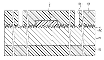
図9は、図3に示すエンコーダースケールの製造方法を説明するためのフローチャートである。図10は、図9に示すエッチング工程における基材準備工程を説明するための断面図である。図11は、図9に示すエッチング工程における異方性エッチング工程を説明するための断面図である。図12は、図9に示す樹脂層形成工程を説明するための断面図である。図13は、図9に示す金属膜形成工程を説明するための断面図である。図14は、図9に示す外形形成工程におけるマスク形成工程を説明するための断面図である。図15は、図9に示す外形形成工程における金属膜切断工程を説明するための断面図である。図16は、図9に示す外形形成工程における基材切断工程を説明するための断面図である。
(Manufacturing method of encoder scale)
FIG. 9 is a flowchart for explaining a method of manufacturing the encoder scale shown in FIG. FIG. 10 is a cross-sectional view for explaining a base material preparation step in the etching step shown in FIG. FIG. 11 is a cross-sectional view for explaining an anisotropic etching step in the etching step shown in FIG. FIG. 12 is a cross-sectional view for explaining the resin layer forming step shown in FIG. FIG. 13 is a cross-sectional view for explaining the metal film forming step shown in FIG. FIG. 14 is a cross-sectional view for explaining a mask forming step in the outer shape forming step shown in FIG. FIG. 15 is a cross-sectional view for explaining a metal film cutting step in the outer shape forming step shown in FIG. FIG. 16 is a cross-sectional view for explaining a base material cutting step in the outer shape forming step shown in FIG.
エンコーダースケール1の製造方法は、図9に示すように、エッチング工程S10と、樹脂層形成工程S20と、金属膜形成工程S30と、外形形成工程S40と、を有する。以下、各工程を順次説明する。なお、以下では、基材2を(100)単結晶シリコンで構成する場合を例に説明する。
As shown in FIG. 9, the method for manufacturing the
[エッチング工程S10]
まず、図10に示すように、(100)単結晶シリコン基板である基材2aを準備する。この基材2aは、単結晶シリコン基板をそのまま用いてもよいが、必要に応じて、単結晶シリコン基板の一方の面を研削して薄肉化した基板を用いる。
[Etching step S10]
First, as shown in FIG. 10, a base material 2a, which is a (100) single crystal silicon substrate, is prepared. As the base material 2a, a single crystal silicon substrate may be used as it is, but if necessary, a substrate obtained by grinding one surface of the single crystal silicon substrate to make it thinner is used.
次に、図11に示すように、基材2aの一方の面(上面)を一様に異方性エッチングする。これにより、複数の凸部21を有する基材2bが得られる。ここで、基材2aの他方の面にレジスト材料等の保護膜を設けてもよいし、基材2aの他方の面にも複数の凸部21を形成してもよい。
Next, as shown in FIG. 11, one surface (upper surface) of the base material 2a is uniformly anisotropically etched. As a result, the
この異方性エッチング(ウェットエッチング)は、特に限定されないが、例えば、KOHやTMAH等のアルカリエッチング液を用いる。 This anisotropic etching (wet etching) is not particularly limited, but for example, an alkaline etching solution such as KOH or TMAH is used.
[樹脂層形成工程S20]
次に、図12に示すように、樹脂層3を形成する。より具体的には、基材2bの上面(複数の凸部21を有する面)に、感光前の感光性樹脂を一様に塗布し、露光および現像することで、樹脂層3を形成する。ここで、現像後、必要に応じて、CMP(chemical mechanical polishing)等の平坦化処理を行って、樹脂層3を形成してもよい。
[Resin layer forming step S20]
Next, as shown in FIG. 12, the
[金属膜形成工程S30]
次に、図13に示すように、金属膜4aを形成する。より具体的には、基材2bおよび樹脂層3からなる積層体の樹脂層3側の面に一様にスパッタ法等により金属材料を成膜することで、金属膜4aを形成する。
[Metal film forming step S30]
Next, as shown in FIG. 13, a
[外形形成工程S40]
次に、エンコーダースケール1の外形(孔11を含む)を形成する。より具体的には、図14に示すように、基材2b、樹脂層3および金属膜4aからなる積層体の両面にマスク(保護膜)としてレジスト層51、52を形成した後に、図15に示すように、レジスト層51の開口511を介したウェットエッチング等により金属膜4aの一部を除去することで切断し、その後、図16に示すように、開口511を介したドライエッチングにより基材2bの一部を除去することで切断する。その後、図示しないが、レジスト層51、52を除去する。
[Outer shape forming step S40]
Next, the outer shape (including the hole 11) of the
本工程において基材2bの切断に用いるドライエッチングとしては、特に限定されないが、例えば、Si高速エッチング法、ボッシュプロセス法、反応性イオンエッチング(RIE:Reactive Ion Etching)、ICP(Inductively Coupled Plasma)等が挙げられる。また、エッチングガスとしては、Cl2+HBr、SF6等を用いることができる。
以上のようにして、エンコーダースケール1を製造することができる。
The dry etching used for cutting the
As described above, the
以上のように、エンコーダースケール1の製造方法は、板状の基材2aの一方の面に、異方性エッチングを行って、基材2aの厚さ方向を法線とする面に対して傾斜している面(傾斜面211)を主体に構成されている第1領域を形成する工程と、基材2aの一方の面上に、感光性樹脂を塗布し、パターニングすることにより樹脂層3を形成した後に、樹脂層3上に金属膜4aを成膜することにより、基材2aの厚さ方向を法線とする面を主体に構成されている第2領域を形成する工程と、を含む。このようなエンコーダースケール1の製造方法によれば、低コスト化を図りつつ、検出精度を高めることができるエンコーダースケール1を得ることができる。
As described above, in the method for manufacturing the
ここで、エッチング工程S10、樹脂層形成工程S20をこの順で行うことで、第1領域121および第2領域122の寸法精度を極めて高くすることができる。これに対し、仮に樹脂層形成工程S20、エッチング工程S10の順で行うと、エッチング工程S10の際、基材2の周方向での位置によってエッチング状態(特にサイドエッチング量)が異なることに起因して、樹脂層の両端が浮いた状態となり、密着性低下による破壊のリスクが生じる。
Here, by performing the etching step S10 and the resin layer forming step S20 in this order, the dimensional accuracy of the
<第2実施形態>
図17は、本発明の第2実施形態に係るエンコーダースケールを示す断面図である。なお、以下の説明では、本実施形態に関し、前述した実施形態との相違点を中心に説明し、同様の事項に関してはその説明を省略する。
<Second Embodiment>
FIG. 17 is a cross-sectional view showing an encoder scale according to a second embodiment of the present invention. In the following description, the present embodiment will be mainly described with respect to the differences from the above-described embodiment, and the description of the same matters will be omitted.
図17に示すエンコーダースケール1Aは、板状をなす基材2Aを有し、その一方の面には、エンコーダースケール1Aの図中方向Eでの移動量、移動速度等を検出し得るパターンとして、方向Eに沿って第1領域121および第2領域122を交互に並べた光学パターン12Aが形成されている。このようなエンコーダースケール1Aは、リニアエンコーダーに用いることができる。
The
ここで、光学パターン12Aの第1領域121および第2領域122は、それぞれ、平面視で、方向Eに直交する方向Dに沿って延びている。また、平面視で、第1領域121および第2領域122の幅がそれぞれ方向Dにわたって一定となっている。また、基材2Aの平面視での形状も、方向Eを長辺とする長方形となっている。
Here, the
このようなエンコーダースケール1Aは、前述した第1実施形態と同様、(100)単結晶シリコンを用いて簡単かつ高精度に形成することができ、この場合、結晶方位(110)が方向Dに沿っていることが好ましい。これにより、第1領域121および第2領域122の寸法精度を容易に高めることができる。
Such an
以上のような第2実施形態のエンコーダースケール1Aによっても、前述した第1実施形態と同様、低コスト化を図りつつ、検出精度を高めることができる。
The
(ロボット)
以下、本発明のロボットについて単腕ロボットを例に説明する。
(robot)
Hereinafter, the robot of the present invention will be described by taking a single-arm robot as an example.
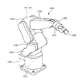
図18は、本発明のロボットの実施形態を示す斜視図である。
図18に示すロボット1000は、精密機器やこれを構成する部品(対象物)の給材、除材、搬送および組立等の作業を行うことができる。このロボット1000は、6軸ロボットであり、床や天井に固定されるベース1010と、ベース1010に回動自在に連結されたアーム1020と、アーム1020に回動自在に連結されたアーム1030と、アーム1030に回動自在に連結されたアーム1040と、アーム1040に回動自在に連結されたアーム1050と、アーム1050に回動自在に連結されたアーム1060と、アーム1060に回動自在に連結されたアーム1070と、これらアーム1020、1030、1040、1050、1060、1070の駆動を制御する制御部1080と、を有している。また、アーム1070にはハンド接続部が設けられており、ハンド接続部にはロボット1000に実行させる作業に応じたエンドエフェクター1090が装着されている。
FIG. 18 is a perspective view showing an embodiment of the robot of the present invention.
The
また、ロボット1000が有する複数の関節部のうちの全部または一部には、エンコーダー10が搭載されており、制御部1080は、このエンコーダー10の出力に基づいて、関節部の駆動を制御する。なお、図示では、エンコーダー10は、アーム1040とアーム1050との間の関節部に設けられている。
Further, an
以上のようなロボット1000は、エンコーダースケール1または1Aを備える。このようなロボット1000によれば、エンコーダースケール1または1Aの低コスト化を図ることで、ロボット1000の低コスト化を図ることができる。また、エンコーダースケール1または1Aを用いた高精度な検出結果に基づいて高精度な動作制御を行うことができる。
The
なお、ロボット1000が有するアームの数は、図示では6本であるが、これに限定されず、1〜5本または7本以上であってもよい。
The number of arms possessed by the
(電子部品搬送装置)
次に、本発明の電子部品搬送装置の実施形態について説明する。
(Electronic component transfer device)
Next, an embodiment of the electronic component transfer device of the present invention will be described.
図19は、本発明の電子部品搬送装置の実施形態を示す斜視図である。なお、以下では、説明の便宜上、互いに直交する3軸をX軸、Y軸およびZ軸とする。 FIG. 19 is a perspective view showing an embodiment of the electronic component transfer device of the present invention. In the following, for convenience of explanation, the three axes orthogonal to each other will be referred to as an X-axis, a Y-axis, and a Z-axis.
図19に示す電子部品搬送装置2000は、電子部品検査装置に適用されており、基台2100と、基台2100の側方に配置された支持台2200と、を有している。また、基台2100には、検査対象の電子部品Qが載置されてY軸方向に搬送される上流側ステージ2110と、検査済みの電子部品Qが載置されてY軸方向に搬送される下流側ステージ2120と、上流側ステージ2110と下流側ステージ2120との間に位置し、電子部品Qの電気的特性を検査する検査台2130と、が設けられている。なお、電子部品Qの例として、例えば、半導体、半導体ウェハー、CLDやOLED等の表示デバイス、水晶デバイス、各種センサー、インクジェットヘッド、各種MEMSデバイス等などが挙げられる。
The electronic
また、支持台2200には、支持台2200に対してY軸方向に移動可能なYステージ2210が設けられており、Yステージ2210には、Yステージ2210に対してX軸方向に移動可能なXステージ2220が設けられており、Xステージ2220には、Xステージ2220に対してZ軸方向に移動可能な電子部品保持部2230が設けられている。
Further, the
また、電子部品保持部2230は、電子部品Qを保持する保持部2233を有し、保持部2233のX軸方向およびY軸方向の位置およびZ軸まわりの姿勢を微調整可能に構成されている。ここで、電子部品保持部2230は、保持部2233のZ軸まわりの姿勢を検出するエンコーダー10を有する。
Further, the electronic
以上のような電子部品搬送装置2000は、エンコーダースケール1または1Aを備える。このような電子部品搬送装置2000によれば、エンコーダースケール1または1Aの低コスト化を図ることで、電子部品搬送装置2000の低コスト化を図ることができる。また、エンコーダースケール1を用いた高精度な検出結果に基づいて高精度な動作制御を行うことができる。
The electronic
(プリンター)
図20は、本発明のプリンターの実施形態を示す斜視図である。
図20に示すプリンター3000は、インクジェット記録方式のプリンターである。このプリンター3000は、装置本体3010と、装置本体3010の内部に設けられている印刷機構3020、給紙機構3030および制御部3040と、を備えている。
(printer)
FIG. 20 is a perspective view showing an embodiment of the printer of the present invention.
The
装置本体3010には、記録用紙Pを設置するトレイ3011と、記録用紙Pを排出する排紙口3012と、液晶ディスプレイ等の操作パネル3013とが設けられている。
The apparatus
印刷機構3020は、ヘッドユニット3021と、キャリッジモーター3022と、キャリッジモーター3022の駆動力によりヘッドユニット3021を往復動させる往復動機構3023と、を備えている。ヘッドユニット3021は、インクジェット式記録ヘッドであるヘッド3021aと、ヘッド3021aにインクを供給するインクカートリッジ3021bと、ヘッド3021aおよびインクカートリッジ3021bを搭載したキャリッジ3021cと、を有している。往復動機構3023は、キャリッジ3021cを往復移動可能に支持しているキャリッジガイド軸3023aと、キャリッジモーター3022の駆動力によりキャリッジ3021cをキャリッジガイド軸3023a上で移動させるタイミングベルト3023bと、を有している。
The
給紙機構3030は、互いに圧接している従動ローラー3031および駆動ローラー3032と、駆動ローラー3032を駆動する給紙モーター3033と、給紙モーター3033の回転軸の回転状態を検出するエンコーダー10と、を有している。
The
制御部3040は、例えばパーソナルコンピュータ等のホストコンピュータから入力された印刷データに基づいて、印刷機構3020や給紙機構3030等を制御する。
The
このようなプリンター3000では、給紙機構3030が記録用紙Pを一枚ずつヘッドユニット3021の下部近傍へ間欠送りする。このとき、ヘッドユニット3021が記録用紙Pの送り方向とほぼ直交する方向に往復移動して、記録用紙Pへの印刷が行なわれる。
In such a
以上のようなプリンター3000は、エンコーダースケール1または1Aを備える。このようなプリンター3000によれば、エンコーダースケール1または1Aの低コスト化を図ることで、プリンター3000の低コスト化を図ることができる。また、エンコーダースケール1または1Aを用いた高精度な検出結果に基づいて高精度な動作制御を行うことができる。
The
(プロジェクター)
図21は、本発明のプロジェクターの実施形態を示す概略図である。
(projector)
FIG. 21 is a schematic view showing an embodiment of the projector of the present invention.
図21に示すプロジェクター4000は、赤色光を出射する光源4100Rと、緑色光を出射する光源4100Gと、青色光を出射する光源4100Bと、レンズアレイ4200R、4200G、4200Bと、透過型の液晶ライトバルブ(光変調部)4300R、4300G、4300Bと、クロスダイクロイックプリズム4400と、投射レンズ(投射部)4500と、圧電駆動装置4700と、を有している。
The
光源4100R、4100G、4100Bから出射された光は、各レンズアレイ4200R、4200G、4200Bを介して、液晶ライトバルブ4300R、4300G、4300Bに入射する。各液晶ライトバルブ4300R、4300G、4300Bは、入射した光をそれぞれ画像情報に応じて変調する。
The light emitted from the
各液晶ライトバルブ4300R、4300G、4300Bによって変調された3つの色光は、クロスダイクロイックプリズム4400に入射して合成される。クロスダイクロイックプリズム4400によって合成された光は、投射光学系である投射レンズ4500に入射する。投射レンズ4500は、液晶ライトバルブ4300R、4300G、4300Bによって形成された像を拡大して、スクリーン(表示面)4600に投射する。これにより、スクリーン4600上に所望の映像が映し出される。ここで、投射レンズ4500は、圧電駆動装置4700に支持されており、圧電駆動装置4700の駆動により位置および姿勢の変更(位置決め)が可能となっている。これにより、スクリーン4600に投射される映像の形状や大きさ等を調整することができる。この圧電駆動装置4700は、その駆動状態を検出するためのエンコーダー10を有する。
The three colored lights modulated by each liquid
なお、上述の例では、光変調部として透過型の液晶ライトバルブを用いたが、液晶以外のライトバルブを用いてもよいし、反射型のライトバルブを用いてもよい。このようなライトバルブとしては、例えば、反射型の液晶ライトバルブや、デジタルマイクロミラーデバイス(Digital Micromirror Device)が挙げられる。また、投射光学系の構成は、使用されるライトバルブの種類によって適宜変更される。また、プロジェクターとしては、光をスクリーン上で走査させることにより、表示面に所望の大きさの画像を表示させる走査型のプロジェクターであってもよい。 In the above example, a transmissive liquid crystal light bulb is used as the light modulation unit, but a light bulb other than the liquid crystal may be used, or a reflective light bulb may be used. Examples of such a light bulb include a reflective liquid crystal light bulb and a digital micromirror device. Further, the configuration of the projection optical system is appropriately changed depending on the type of the light bulb used. Further, the projector may be a scanning type projector that displays an image of a desired size on a display surface by scanning light on a screen.
以上のようなプロジェクター4000は、エンコーダースケール1または1Aを備える。このようなプロジェクター4000によれば、エンコーダースケール1または1Aの低コスト化を図ることで、プロジェクター4000の低コスト化を図ることができる。また、エンコーダースケール1または1Aを用いた高精度な検出結果に基づいて高精度な動作制御を行うことができる。
The
以上、本発明のエンコーダースケール、エンコーダースケールの製造方法、エンコーダー、ロボット、電子部品搬送装置、プリンターおよびプロジェクターを、図示の実施形態に基づいて説明したが、本発明はこれに限定されるものではなく、各部の構成は、同様の機能を有する任意の構成のものに置換することができる。また、本発明に、他の任意の構成物が付加されていてもよい。 The encoder scale, the method for manufacturing the encoder scale, the encoder, the robot, the electronic component transfer device, the printer, and the projector of the present invention have been described above based on the illustrated embodiments, but the present invention is not limited thereto. , The configuration of each part can be replaced with an arbitrary configuration having the same function. Further, any other constituents may be added to the present invention.
また、本発明は、前述した実施形態のうちの、任意の2以上の構成(特徴)を組み合わせたものであってもよい。 Further, the present invention may be a combination of any two or more configurations (features) of the above-described embodiments.
また、本発明のロボットは、アームを有していれば、単腕ロボットに限定されず、例えば、双腕ロボット、スカラーロボット等の他のロボットであってもよい。 Further, the robot of the present invention is not limited to a single-arm robot as long as it has an arm, and may be, for example, another robot such as a double-arm robot or a scalar robot.
また、前述した実施形態ではエンコーダースケールユニットおよびエンコーダーをロボットおよびプリンターに適用した構成について説明したが、エンコーダースケールユニットおよびエンコーダーは、これら以外の各種電子機器にも適用することができる。また、エンコーダーは、プリンターに用いる場合、プリンターの紙送りローラーの駆動源に限定されず、例えば、プリンターのインクジェットヘッドの駆動源等に適用することもできる。 Further, in the above-described embodiment, the configuration in which the encoder scale unit and the encoder are applied to the robot and the printer has been described, but the encoder scale unit and the encoder can also be applied to various electronic devices other than these. When used in a printer, the encoder is not limited to the drive source of the paper feed roller of the printer, and can be applied to, for example, the drive source of the inkjet head of the printer.
また、本発明のエンコーダーは、ロボット以外の機器に組み込んでもよく、例えば、自動車等の移動体に搭載してもよい。 Further, the encoder of the present invention may be incorporated in a device other than a robot, and may be mounted on a moving body such as an automobile, for example.
1…エンコーダースケール、1A…エンコーダースケール、2…基材、2A…基材、2a…基材、2b…基材、3…樹脂層、4…金属膜、4a…金属膜、10…エンコーダー、11…孔、12…光学パターン、12A…光学パターン、20…回転軸、21…凸部、22…凸部、30…エンコーダースケールユニット、40…光学センサー、41…反射面、42…反射面、51…レジスト層、52…レジスト層、121…第1領域、122…第2領域、211…傾斜面、301…ハブ、302…接着剤、303…支持部、304…突出部、305…凸部、306…凹部、307…設置面、401…基板、402…光源部、403…受光部、511…開口、1000…ロボット、1010…ベース、1020…アーム、1030…アーム、1040…アーム、1050…アーム、1060…アーム、1070…アーム、1080…制御部、1090…エンドエフェクター、2000…電子部品搬送装置、2100…基台、2110…上流側ステージ、2120…下流側ステージ、2130…検査台、2200…支持台、2210…Yステージ、2220…Xステージ、2230…電子部品保持部、2233…保持部、3000…プリンター、3010…装置本体、3011…トレイ、3012…排紙口、3013…操作パネル、3020…印刷機構、3021…ヘッドユニット、3021a…ヘッド、3021b…インクカートリッジ、3021c…キャリッジ、3022…キャリッジモーター、3023…往復動機構、3023a…キャリッジガイド軸、3023b…タイミングベルト、3030…給紙機構、3031…従動ローラー、3032…駆動ローラー、3033…給紙モーター、3040…制御部、4000…プロジェクター、4100B…光源、4100G…光源、4100R…光源、4200B…レンズアレイ、4200G…レンズアレイ、4200R…レンズアレイ、4300B…液晶ライトバルブ、4300G…液晶ライトバルブ、4300R…液晶ライトバルブ、4400…クロスダイクロイックプリズム、4500…投射レンズ、4600…スクリーン、4700…圧電駆動装置、B…延在方向、C…延在方向、D…方向、E…方向、LL…光、P…記録用紙、Q…電子部品、S10…エッチング工程、S20…樹脂層形成工程、S30…金属膜形成工程、S40…外形形成工程、ax…軸線、h…高さ、θ…傾斜角度、t1…厚さ、t2…厚さ
1 ... Encoder scale, 1A ... Encoder scale, 2 ... Base material, 2A ... Base material, 2a ... Base material, 2b ... Base material, 3 ... Resin layer, 4 ... Metal film, 4a ... Metal film, 10 ... Encoder, 11 ... Hole, 12 ... Optical pattern, 12A ... Optical pattern, 20 ... Rotation axis, 21 ... Convex part, 22 ... Convex part, 30 ... Encoder scale unit, 40 ... Optical sensor, 41 ... Reflective surface, 42 ... Reflective surface, 51 ... Resist layer, 52 ... Resist layer, 121 ... First region, 122 ... Second region, 211 ... Inclined surface, 301 ... Hub, 302 ... Adhesive, 303 ... Support part, 304 ... Protruding part, 305 ... Convex part, 306 ... recess, 307 ... installation surface, 401 ... substrate, 402 ... light source, 403 ... light receiving, 511 ... opening, 1000 ... robot, 1010 ... base, 1020 ... arm, 1030 ... arm, 1040 ... arm, 1050 ...
Claims (12)
前記基材の一方の面に設けられ、第1領域と第2領域とが交互に並んでいる光学パターンと、を備え、
前記第1領域は、
前記基材上に配置されて、感光性樹脂を含む樹脂層と、
前記樹脂層上に配置された金属膜と、を有し、
前記第1領域の表面は、前記基材の厚さ方向を法線とする第1面を主体に構成され、
前記第2領域の表面は、前記第1面に対して傾斜している第2面を主体に構成されていることを特徴とするエンコーダースケール。 Plate-shaped base material and
An optical pattern provided on one surface of the base material and in which a first region and a second region are alternately arranged is provided.
The first region is
Is placed on the substrate, a resin layer containing a photosensitive resin,
It has a metal film arranged on the resin layer and
The surface of the first region is mainly composed of the first surface having the thickness direction of the base material as a normal.
An encoder scale characterized in that the surface of the second region is mainly composed of a second surface that is inclined with respect to the first surface.
前記一方の面上に、感光性樹脂を塗布し、パターニングすることにより樹脂層を形成した後に、前記樹脂層上に金属膜を成膜することにより、前記基材の厚さ方向を法線とする面を主体に構成されている第2領域を形成する工程と、を含むことを特徴とするエンコーダースケールの製造方法。 A first region formed mainly of a surface that is anisotropically etched on one surface of a plate-shaped substrate and is inclined with respect to a surface whose normal is the thickness direction of the substrate. And the process of forming
A photosensitive resin is applied onto one of the surfaces to form a resin layer by patterning, and then a metal film is formed on the resin layer so that the thickness direction of the base material becomes a normal. A method for manufacturing an encoder scale, which comprises a step of forming a second region mainly composed of a surface to be formed.
前記エンコーダースケールに向けて光を出射する光出射部と、
前記エンコーダースケールで反射した前記光を検出する光検出部と、を備えることを特徴とするエンコーダー。 The encoder scale according to any one of claims 1 to 6 and the encoder scale.
A light emitting unit that emits light toward the encoder scale,
An encoder including a photodetector for detecting the light reflected by the encoder scale.
Priority Applications (3)
| Application Number | Priority Date | Filing Date | Title |
|---|---|---|---|
| JP2017209385A JP6958237B2 (en) | 2017-10-30 | 2017-10-30 | Encoder scales, encoder scale manufacturing methods, encoders, robots, electronic component transfer devices, printers and projectors |
| CN201811264212.5A CN109724635B (en) | 2017-10-30 | 2018-10-26 | Encoder scale, method for manufacturing encoder scale, and encoder |
| US16/173,023 US10955265B2 (en) | 2017-10-30 | 2018-10-29 | Encoder scale, manufacturing method for encoder scale, and encoder |
Applications Claiming Priority (1)
| Application Number | Priority Date | Filing Date | Title |
|---|---|---|---|
| JP2017209385A JP6958237B2 (en) | 2017-10-30 | 2017-10-30 | Encoder scales, encoder scale manufacturing methods, encoders, robots, electronic component transfer devices, printers and projectors |
Publications (3)
| Publication Number | Publication Date |
|---|---|
| JP2019082376A JP2019082376A (en) | 2019-05-30 |
| JP2019082376A5 JP2019082376A5 (en) | 2020-12-10 |
| JP6958237B2 true JP6958237B2 (en) | 2021-11-02 |
Family
ID=66242839
Family Applications (1)
| Application Number | Title | Priority Date | Filing Date |
|---|---|---|---|
| JP2017209385A Active JP6958237B2 (en) | 2017-10-30 | 2017-10-30 | Encoder scales, encoder scale manufacturing methods, encoders, robots, electronic component transfer devices, printers and projectors |
Country Status (3)
| Country | Link |
|---|---|
| US (1) | US10955265B2 (en) |
| JP (1) | JP6958237B2 (en) |
| CN (1) | CN109724635B (en) |
Families Citing this family (2)
| Publication number | Priority date | Publication date | Assignee | Title |
|---|---|---|---|---|
| EP3399284B1 (en) * | 2017-05-03 | 2019-07-10 | Dr. Johannes Heidenhain GmbH | Sensor unit for position measurement |
| WO2023035476A1 (en) * | 2021-09-09 | 2023-03-16 | 深圳市汇顶科技股份有限公司 | Optical encoder and electronic device |
Family Cites Families (11)
| Publication number | Priority date | Publication date | Assignee | Title |
|---|---|---|---|---|
| JPH04211202A (en) * | 1990-03-19 | 1992-08-03 | Canon Inc | Reflection type diffraction grating and device by use of same deffraction grating |
| US5916735A (en) * | 1996-11-21 | 1999-06-29 | Matsushita Electric Industrial Co., Ltd. | Method for manufacturing fine pattern |
| DE19937023A1 (en) * | 1999-08-05 | 2001-02-08 | Heidenhain Gmbh Dr Johannes | Reflection material measure and method for producing a reflection material measure |
| DE10150099A1 (en) * | 2001-10-11 | 2003-04-17 | Heidenhain Gmbh Dr Johannes | Production of a measuring rod used for electrical position measuring device comprises applying spacer layer on first reflecting layer, applying second reflecting layer, and structuring second reflecting layer by electron beam lithography |
| US20040175843A1 (en) * | 2003-03-04 | 2004-09-09 | Roitman Daniel B. | Near-field and far-field encoding and shaping of microbeads for bioassays |
| EP2187177A4 (en) * | 2007-09-05 | 2012-12-26 | Nikon Corp | Reflector plate for optical encoder, method for producing the same, and optical encoder |
| JP5562152B2 (en) * | 2010-07-12 | 2014-07-30 | Dmg森精機株式会社 | Diffraction grating |
| KR101856231B1 (en) * | 2011-12-19 | 2018-05-10 | 엘지이노텍 주식회사 | Transparent substrate with nano-pattern and method of manufacturing thereof |
| JP5420715B2 (en) * | 2012-05-28 | 2014-02-19 | オリンパス株式会社 | Reflective optical encoder |
| JP6079122B2 (en) * | 2012-10-12 | 2017-02-15 | 日立金属株式会社 | Optical substrate, optical substrate manufacturing method, and optical module structure |
| JP6253929B2 (en) * | 2013-09-11 | 2017-12-27 | 株式会社オプトニクス精密 | Reflective encoder device |
-
2017
- 2017-10-30 JP JP2017209385A patent/JP6958237B2/en active Active
-
2018
- 2018-10-26 CN CN201811264212.5A patent/CN109724635B/en active Active
- 2018-10-29 US US16/173,023 patent/US10955265B2/en active Active
Also Published As
| Publication number | Publication date |
|---|---|
| CN109724635B (en) | 2022-04-15 |
| JP2019082376A (en) | 2019-05-30 |
| US10955265B2 (en) | 2021-03-23 |
| US20190128706A1 (en) | 2019-05-02 |
| CN109724635A (en) | 2019-05-07 |
Similar Documents
| Publication | Publication Date | Title |
|---|---|---|
| JP6414308B2 (en) | Pattern forming device | |
| JP4408351B2 (en) | Alignment device | |
| JP6958237B2 (en) | Encoder scales, encoder scale manufacturing methods, encoders, robots, electronic component transfer devices, printers and projectors | |
| CN104792344A (en) | Detector, imprint apparatus, and article manufacturing method | |
| JP2006237501A (en) | Positioning method of semiconductor wafer and device using it | |
| JP2018191437A (en) | Piezoelectric drive device, electronic component transfer device, robot, projector, and printer | |
| US10782160B2 (en) | Encoder scale, method for manufacturing encoder scale, encoder, robot, and printer | |
| JP2005156549A (en) | Optical encoder | |
| JP2019095316A (en) | Encoder scale, method for manufacturing encoder scale, encoder, robot, printer, and projector | |
| US9217937B2 (en) | Interferometric measurement of rotation of stage apparatus and adjustment method thereof, exposure apparatus and method of manufacturing device | |
| CN109571462B (en) | Encoder, printer, and robot | |
| JP6413784B2 (en) | Substrate processing apparatus and device manufacturing method | |
| JP6748428B2 (en) | Lithographic apparatus, article manufacturing method, stage apparatus, and measuring apparatus | |
| JP6680330B2 (en) | Pattern forming equipment | |
| JP2019146364A (en) | Piezoelectric drive device, robot, electronic component conveying device, printer, and projector | |
| JP2009121920A (en) | Transparent substrate position measuring apparatus, exposure apparatus provided with the position measuring apparatus, substrate measuring method, and prealignment apparatus | |
| JP6114861B2 (en) | Imprint apparatus, imprint method, and article manufacturing method | |
| US20190128707A1 (en) | Optical Scale, Encoder, Robot, Electronic-Component Conveying Apparatus, Printer, And Projector | |
| US20230001608A1 (en) | Conveyance apparatus, planarization apparatus, and article manufacturing method | |
| JP2019068545A (en) | Piezoelectric drive device, robot, electronic component conveyance apparatus, printer, and projector | |
| JP6996580B2 (en) | Board processing method | |
| WO2021111918A1 (en) | Foreign matter inspection device, foreign matter inspection method, processing device, and article manufacturing method | |
| JP4497364B2 (en) | Alignment method and alignment apparatus in proximity exposure | |
| JP4335781B2 (en) | Exposure apparatus and exposure method | |
| JPH1012709A (en) | Circular substrate positioning device |
Legal Events
| Date | Code | Title | Description |
|---|---|---|---|
| A521 | Request for written amendment filed |
Free format text: JAPANESE INTERMEDIATE CODE: A523 Effective date: 20201029 |
|
| A621 | Written request for application examination |
Free format text: JAPANESE INTERMEDIATE CODE: A621 Effective date: 20201029 |
|
| A977 | Report on retrieval |
Free format text: JAPANESE INTERMEDIATE CODE: A971007 Effective date: 20210826 |
|
| TRDD | Decision of grant or rejection written | ||
| A01 | Written decision to grant a patent or to grant a registration (utility model) |
Free format text: JAPANESE INTERMEDIATE CODE: A01 Effective date: 20210907 |
|
| A61 | First payment of annual fees (during grant procedure) |
Free format text: JAPANESE INTERMEDIATE CODE: A61 Effective date: 20210920 |
|
| R150 | Certificate of patent or registration of utility model |
Ref document number: 6958237 Country of ref document: JP Free format text: JAPANESE INTERMEDIATE CODE: R150 |