JP6254445B2 - Charged particle beam equipment - Google Patents
Charged particle beam equipment Download PDFInfo
- Publication number
- JP6254445B2 JP6254445B2 JP2014002260A JP2014002260A JP6254445B2 JP 6254445 B2 JP6254445 B2 JP 6254445B2 JP 2014002260 A JP2014002260 A JP 2014002260A JP 2014002260 A JP2014002260 A JP 2014002260A JP 6254445 B2 JP6254445 B2 JP 6254445B2
- Authority
- JP
- Japan
- Prior art keywords
- voltage
- deflector
- electric field
- magnetic field
- source circuit
- Prior art date
- Legal status (The legal status is an assumption and is not a legal conclusion. Google has not performed a legal analysis and makes no representation as to the accuracy of the status listed.)
- Active
Links
Images


Classifications
-
- H—ELECTRICITY
- H01—ELECTRIC ELEMENTS
- H01J—ELECTRIC DISCHARGE TUBES OR DISCHARGE LAMPS
- H01J37/00—Discharge tubes with provision for introducing objects or material to be exposed to the discharge, e.g. for the purpose of examination or processing thereof
- H01J37/02—Details
- H01J37/04—Arrangements of electrodes and associated parts for generating or controlling the discharge, e.g. electron-optical arrangement, ion-optical arrangement
- H01J37/147—Arrangements for directing or deflecting the discharge along a desired path
- H01J37/1472—Deflecting along given lines
-
- H—ELECTRICITY
- H01—ELECTRIC ELEMENTS
- H01J—ELECTRIC DISCHARGE TUBES OR DISCHARGE LAMPS
- H01J37/00—Discharge tubes with provision for introducing objects or material to be exposed to the discharge, e.g. for the purpose of examination or processing thereof
- H01J37/02—Details
- H01J37/244—Detectors; Associated components or circuits therefor
-
- H—ELECTRICITY
- H01—ELECTRIC ELEMENTS
- H01J—ELECTRIC DISCHARGE TUBES OR DISCHARGE LAMPS
- H01J37/00—Discharge tubes with provision for introducing objects or material to be exposed to the discharge, e.g. for the purpose of examination or processing thereof
- H01J37/26—Electron or ion microscopes; Electron or ion diffraction tubes
- H01J37/28—Electron or ion microscopes; Electron or ion diffraction tubes with scanning beams
-
- H—ELECTRICITY
- H01—ELECTRIC ELEMENTS
- H01J—ELECTRIC DISCHARGE TUBES OR DISCHARGE LAMPS
- H01J2237/00—Discharge tubes exposing object to beam, e.g. for analysis treatment, etching, imaging
- H01J2237/15—Means for deflecting or directing discharge
- H01J2237/1504—Associated circuits
-
- H—ELECTRICITY
- H01—ELECTRIC ELEMENTS
- H01J—ELECTRIC DISCHARGE TUBES OR DISCHARGE LAMPS
- H01J2237/00—Discharge tubes exposing object to beam, e.g. for analysis treatment, etching, imaging
- H01J2237/15—Means for deflecting or directing discharge
- H01J2237/1508—Combined electrostatic-electromagnetic means
-
- H—ELECTRICITY
- H01—ELECTRIC ELEMENTS
- H01J—ELECTRIC DISCHARGE TUBES OR DISCHARGE LAMPS
- H01J2237/00—Discharge tubes exposing object to beam, e.g. for analysis treatment, etching, imaging
- H01J2237/15—Means for deflecting or directing discharge
- H01J2237/152—Magnetic means
-
- H—ELECTRICITY
- H01—ELECTRIC ELEMENTS
- H01J—ELECTRIC DISCHARGE TUBES OR DISCHARGE LAMPS
- H01J2237/00—Discharge tubes exposing object to beam, e.g. for analysis treatment, etching, imaging
- H01J2237/153—Correcting image defects, e.g. stigmators
- H01J2237/1534—Aberrations
-
- H—ELECTRICITY
- H01—ELECTRIC ELEMENTS
- H01J—ELECTRIC DISCHARGE TUBES OR DISCHARGE LAMPS
- H01J2237/00—Discharge tubes exposing object to beam, e.g. for analysis treatment, etching, imaging
- H01J2237/26—Electron or ion microscopes
- H01J2237/28—Scanning microscopes
- H01J2237/2803—Scanning microscopes characterised by the imaging method
- H01J2237/2804—Scattered primary beam
-
- H—ELECTRICITY
- H01—ELECTRIC ELEMENTS
- H01J—ELECTRIC DISCHARGE TUBES OR DISCHARGE LAMPS
- H01J2237/00—Discharge tubes exposing object to beam, e.g. for analysis treatment, etching, imaging
- H01J2237/26—Electron or ion microscopes
- H01J2237/28—Scanning microscopes
- H01J2237/2803—Scanning microscopes characterised by the imaging method
- H01J2237/2806—Secondary charged particle
Landscapes
- Chemical & Material Sciences (AREA)
- Analytical Chemistry (AREA)
- Testing Or Measuring Of Semiconductors Or The Like (AREA)
Description
本発明は、半導体基板(ウェハ)などの試料(対象物)の計測、あるいは観察、または検査などの処理を行う計測検査装置、及びそれを用いて計測、または検査などを行う計測検査方法に関し、特に、荷電粒子装置の一つとして走査型電子顕微鏡装置(以下、SEMと略す)を用いて試料を撮像し、計測、あるいは観察、または検査を行う処理装置、及びその計測・検査方法に関する。 The present invention relates to a measurement / inspection apparatus that performs processing such as measurement, observation, or inspection of a sample (object) such as a semiconductor substrate (wafer), and a measurement / inspection method that performs measurement or inspection using the same, In particular, the present invention relates to a processing apparatus that images a sample by using a scanning electron microscope apparatus (hereinafter abbreviated as SEM) as one of charged particle apparatuses and performs measurement, observation, or inspection, and a measurement / inspection method thereof.
半導体製造プロセスにおいて、半導体基板(ウェハ)上に形成される回路パターンの微細化が急速に進んでおり、それらのパターンが設計通りに形成されているか否か等を監視するプロセスモニタリングの重要性が益々増加している。例えば、半導体製造プロセスにおける異常や不良(欠陥)の発生を早期に、あるいは事前に検知するために、各製造工程の終了時にウェハ上の回路パターン等の計測及び検査が行われる。 In semiconductor manufacturing processes, circuit patterns formed on a semiconductor substrate (wafer) are rapidly miniaturized, and the importance of process monitoring for monitoring whether these patterns are formed as designed is important. Increasingly. For example, in order to detect an abnormality or defect (defect) in a semiconductor manufacturing process early or in advance, measurement and inspection of a circuit pattern or the like on a wafer is performed at the end of each manufacturing process.
上記計測・検査の際、走査型電子ビーム方式を用いたSEMなどの計測検査装置及び対応する計測検査方法においては、対象のウェハなどの試料に対して一次電子ビーム(電子線)を走査(スキャン)しながら照射し、これにより発生する二次電子・反射などのエネルギーを検出する。そして、その検出に基づき信号処理・画像処理などにより画像(計測画像や検査画像)を生成し、当該画像に基づいて計測、観察又は検査が行われる。 In the measurement / inspection, in a measurement / inspection apparatus such as an SEM using a scanning electron beam method and a corresponding measurement / inspection method, a primary electron beam (electron beam) is scanned (scanned) on a sample such as a target wafer. ), And detect energy such as secondary electrons and reflections. Based on the detection, an image (measurement image or inspection image) is generated by signal processing or image processing, and measurement, observation, or inspection is performed based on the image.
前記走査型電子ビーム方式を用いた計測装置においては、試料から発生する二次電子・反射電子(二次ビーム)を高効率的に検出するため、二次電子・反射電子を検出器の方に偏向する必要がある。一方、二次ビームを所定の方向に偏向する手段が一次ビームに影響を及ぼすと、一次ビームが試料上の照射位置ずれが発生し、装置の計測精度を劣化する。そのために、二次電子ビームと言う二次電子・反射電子を検出器の設置方向へ偏向し、且つ試料の所定位置に照射する一次ビームを偏向しない一次ビーム・二次ビームの分離手段が必要である。 In the measuring apparatus using the scanning electron beam method, secondary electrons and reflected electrons (secondary beam) generated from the sample are detected with high efficiency. There is a need to deflect. On the other hand, when the means for deflecting the secondary beam in a predetermined direction affects the primary beam, the irradiation position of the primary beam is shifted on the sample, and the measurement accuracy of the apparatus is deteriorated. For this purpose, it is necessary to have a means for separating the primary beam and the secondary beam that deflects secondary electrons and reflected electrons, called secondary electron beams, in the direction of the detector and does not deflect the primary beam that irradiates a predetermined position of the sample. is there.
上記計測・検査および一次電子ビーム・二次電子ビーム分離制御に係わる先行技術例として、特開2006−332038号公報(特許文献1)に記載された技術がある。 As a prior art example related to the above measurement / inspection and primary electron beam / secondary electron beam separation control, there is a technique described in Japanese Patent Laid-Open No. 2006-332038 (Patent Document 1).
特許文献1では、高分解能化可能な電磁界重畳型対物レンズにおいて、試料から発生する二次電子を加速して対物レンズによる回転作用の二次電子エネルギー依存性を抑制し、電子源と対物レンズの間に設けた環状検出器で二次電子の発生箇所から見た仰角の低角成分と、高角成分を選別、さらに方位角成分も選別して検出する際、加速によって細く収束された二次電子の中心軸を低仰角信号検出系の中心軸に合わせると共に、高仰角信号検出系の穴を避けるようにExBで二次電子を調整・偏向することについて記載されている。 In Patent Document 1, in an electromagnetic field superimposed objective lens capable of increasing the resolution, the secondary electrons generated from the sample are accelerated to suppress the secondary electron energy dependency of the rotational action by the objective lens. A secondary detector that is finely converged by acceleration when selecting and detecting the low-angle and high-angle components of the elevation angle as seen from the secondary electron generation location with the annular detector provided between It describes that the center axis of electrons is aligned with the center axis of the low elevation angle signal detection system and that secondary electrons are adjusted and deflected by ExB so as to avoid holes in the high elevation angle signal detection system.
SEMによる計測装置では、計測対象であるウェハ上に形成される回路パターンの微細化と材料の多様化に伴い、計測精度の分解能向上と深溝・穴の見え改善が要求されている。分解能の向上には、一次電子ビームの走査精度向上、つまり一次電子ビームの走査位置ずれの低減を要求される。深い溝・深い穴の見え改善には、二次電子・反射電子の高効率検出をするため、二次ビームの高角度(大角度)偏向が必要である。つまり、二次ビームを偏向する電界・磁界を大きくする高電圧・大電流の制御回路は必須である。 In the measurement apparatus using SEM, with the miniaturization of circuit patterns formed on the wafer to be measured and the diversification of materials, it is required to improve the resolution of measurement accuracy and improve the appearance of deep grooves and holes. In order to improve the resolution, it is required to improve the scanning accuracy of the primary electron beam, that is, to reduce the scanning position deviation of the primary electron beam. In order to improve the visibility of deep grooves and deep holes, high angle (large angle) deflection of the secondary beam is necessary to detect secondary electrons and reflected electrons with high efficiency. That is, a high voltage / current control circuit that increases the electric field / magnetic field for deflecting the secondary beam is essential.
前掲の特許文献1には、一次電子ビーム・二次電子ビーム分離制御に関して、直交電磁界発生器による一次電子線への影響を相殺し且つ二次電子を検出器側に導くように電界と直交する方向に磁界を発生させる方法などについて記載されている。しかし、電界偏向器を制御する電圧源回路と磁界偏向器を制御電流源回路において、回路構成素子で発生した回路ノイズが一次電子ビームの走査位置ずれを発生させる問題に関する解決手段などは開示されていない。 In the above-mentioned Patent Document 1, the primary electron beam / secondary electron beam separation control is orthogonal to the electric field so as to cancel the influence on the primary electron beam by the orthogonal electromagnetic field generator and to guide the secondary electrons to the detector side. It describes a method for generating a magnetic field in the direction in which it is generated. However, in the voltage source circuit for controlling the electric field deflector and the magnetic current deflector in the control current source circuit, there has been disclosed a solution for the problem that circuit noise generated in the circuit constituent element causes a scanning position shift of the primary electron beam. Absent.
そこで、本発明は、二次電子・反射電子の大角度偏向を実現すると共に、電磁偏向器と静電偏向器のノイズを打ち消して一次ビーム/二次ビーム分離回路の回路ノイズが起因する一次電子ビームの位置ずれを抑制する走査型電子顕微鏡を用いた処理装置及び処理方法を提供するものである。 Therefore, the present invention realizes large-angle deflection of secondary electrons and reflected electrons, cancels noises of electromagnetic deflectors and electrostatic deflectors, and causes primary electrons caused by circuit noise of the primary beam / secondary beam separation circuit. It is an object of the present invention to provide a processing apparatus and a processing method using a scanning electron microscope that suppresses beam misalignment.
上記した課題を解決するために、本発明の荷電粒子ビーム装置の主な特徴は、以下の通りである。 In order to solve the above-described problems, main features of the charged particle beam apparatus of the present invention are as follows.
荷電粒子ビームを生成する荷電粒子銃と、該荷電粒子銃から放出された荷電粒子ビームをステージに載置した試料上に照射して走査する電子光学系と、試料から発生する二次電子、または反射電子を検出する検出部と、二次電子、または反射電子の進路を検出部の方向へ偏向させる直交電磁偏向部と、を有し、直交電磁偏向部は、磁界を発生させて荷電粒子ビームの軌跡を変化させる磁界偏向器と、電界を発生させて荷電粒子ビームの軌跡を変化させる電界偏向器と、磁界偏向器に電流を供給する電流源回路と、電界偏向器に電圧を供給する電圧源回路と、電流と電圧との関係を調整するゲイン調整部とを備え、磁界偏向器と電界偏向器は、磁界と前記電界とが互いに直交し重畳するように配置され、電流源回路に電圧を印加する電圧発生部と、電圧源回路に電圧を印加する電圧発生部とが一つに共通化され、ゲイン調整部により、磁界により進路が偏向される量と電界により進路が偏向される量とが一致するように、電流と電圧との関係が調整されることを特徴とする。 A charged particle gun for generating a charged particle beam, an electron optical system for irradiating and scanning a charged particle beam emitted from the charged particle gun on a stage, and secondary electrons generated from the sample, or A detection unit that detects reflected electrons, and an orthogonal electromagnetic deflection unit that deflects the path of secondary electrons or reflected electrons in the direction of the detection unit. The orthogonal electromagnetic deflection unit generates a magnetic field to generate a charged particle beam. A magnetic field deflector that changes the trajectory of the electric field, an electric field deflector that changes the trajectory of the charged particle beam by generating an electric field, a current source circuit that supplies current to the magnetic field deflector, and a voltage that supplies voltage to the electric field deflector A magnetic field deflector and an electric field deflector are arranged so that the magnetic field and the electric field are orthogonally superimposed on each other, and the voltage is applied to the current source circuit. Voltage generator to apply The voltage generator for applying a voltage to the voltage source circuit is shared by one, and the amount of the course being deflected by the magnetic field and the amount of the course being deflected by the electric field are matched by the gain adjuster. The relationship between current and voltage is adjusted.
上記構成によれば、本発明による荷電粒子ビーム装置は、高スループットと高分解能に対応した計測を制御する機能を有すると共に、その際に課題となる、電子ビームを偏向する電界偏向器を制御する電圧源回路と磁界偏向器を制御電流源回路において、回路構成素子で発生した回路ノイズが一次電子ビームの走査位置ずれを発生させる問題に関する解決手段を提供する。 According to the above configuration, the charged particle beam apparatus according to the present invention has a function of controlling measurement corresponding to high throughput and high resolution, and controls an electric field deflector that deflects an electron beam, which is a problem at that time. In a control current source circuit including a voltage source circuit and a magnetic deflector, a solution is provided for a problem that circuit noise generated in a circuit component causes a scanning position shift of a primary electron beam.
即ち、本発明では、分解能とスループットの向上を図るために電流制御コイルで発生する磁界と電圧制御で発生する電界を直交する電磁重畳偏向器(以下、直交電磁偏向器と呼ぶ)による一次電子ビームの走査位置ずれ課題を解決する方策として、静電場を発生する静電偏向器へ印加する電圧源制御信号生成部と、静磁場を発生する電磁偏向器へ印加する電流源制御信号生成部と共通化することと、電圧制御信号の周波数特性および位相特性と電流源制御信号の周波数特性および位相特性と一致することを設けた。これにより回路ノイズに起因する一次電子ビームずれを低減し、高分解能と高スループットな計測を実現した。 That is, in the present invention, in order to improve resolution and throughput, a primary electron beam by an electromagnetic superimposed deflector (hereinafter referred to as an orthogonal electromagnetic deflector) in which a magnetic field generated by a current control coil and an electric field generated by voltage control are orthogonal to each other. As a measure to solve the problem of scan position deviation, a voltage source control signal generator applied to an electrostatic deflector that generates an electrostatic field and a current source control signal generator applied to an electromagnetic deflector that generates a static magnetic field are common. And matching the frequency characteristics and phase characteristics of the voltage control signal with the frequency characteristics and phase characteristics of the current source control signal. As a result, the primary electron beam deviation caused by circuit noise was reduced, and high-resolution and high-throughput measurement was realized.
本発明によれば、二次電子・反射電子の大角度偏向を実現すると共に、電磁偏向器と静電偏向器のノイズを打ち消して一次ビーム/二次ビーム分離回路の回路ノイズが起因する一次電子ビームの位置ずれを抑制する走査型電子顕微鏡を用いた処理装置及び処理方法を提供することができる。 According to the present invention, the primary electron caused by the circuit noise of the primary beam / secondary beam separation circuit by realizing the large angle deflection of the secondary electron and the reflected electron and canceling the noise of the electromagnetic deflector and the electrostatic deflector. It is possible to provide a processing apparatus and a processing method using a scanning electron microscope that suppresses beam misalignment.
以下、図面に基づき、本発明の実施の形態を詳細に説明する。なお実施の形態を説明するための全図において同一部には原則として同一符号を付し、その繰り返しの説明は省略する。以下、計測観察検査装置及び計測観察検査方法とは、計測、観察、検査のうちの何れか一つ又はそれらを組み合わせた場合を含む。 Hereinafter, embodiments of the present invention will be described in detail with reference to the drawings. Note that components having the same function are denoted by the same reference symbols throughout the drawings for describing the embodiment, and the repetitive description thereof will be omitted. Hereinafter, the measurement observation inspection apparatus and the measurement observation inspection method include any one of measurement, observation, and inspection, or a combination thereof.
本発明になる走査型電子ビーム方式の計測検査装置は、図8に示す従来の走査型電子ビーム方式を用いた計測検査装置(システム)を基本構成にし、当該装置構成に本発明になる直交電磁偏向器の制御回路の構成を採り込んでいる。そこで、先ず、図8のシステム構成について説明する。 The scanning electron beam measurement / inspection apparatus according to the present invention is based on the conventional measurement / inspection apparatus (system) using the scanning electron beam system shown in FIG. The configuration of the control circuit of the deflector is adopted. First, the system configuration of FIG. 8 will be described.
従来の計測検査装置(システム)は、大きくは、走査型電子顕微鏡800とコンピュータ820とで構成されている。
A conventional measurement / inspection apparatus (system) is mainly composed of a
走査型電子顕微鏡800は、鏡筒830と試料室840を備え、鏡筒830の内部には、照射系(電子光学系)として、電子ビームA21を射出する電子銃801、射出された電子ビームA21が通る集束レンズ(第1コンデンサレンズ)802、絞り803、集束レンズ(第2コンデンサレンズ)804、ブランキング制御電極805、アパーチャ806、偏向電極808、対物レンズ809等が備えられている。また鏡筒830には、検出系として、照射された電子ビームA21(A24)により試料810から発生した二次電子A211を検出する検出器807を備える。また一次ビームと二次ビームの分離手段として、直交電磁界発生器(ExB)816を備える。
The
コンピュータ820には、全体制御部824と、ブランキング(BLK)制御回路821と、直交電磁偏向器(ExB)822、偏向制御回路823、機構系制御部825と、信号検出部(二次電子信号検出回路)827、画像処理部(二次電子信号処理回路)828、ステージ位置検出部(図示せず)、電子光学系制御部(図示せず)、GUI部(ユーザインタフェース部)826、等を備える。
The computer 820 includes an
鏡筒830の内部(真空状態)において、電子銃801より生成・射出された電子ビームA21は、第1コンデンサレンズ(集束レンズ)802、絞り803、第2コンデンサレンズ(集束レンズ)804を通じて集束され、偏向電極808を介してビームの照射中心に移動と走査偏向制御され、対物レンズ809等を経て試料810上を走査しながら照射される。ビームA21(A24)が照射されると、試料810からは二次電子A211が発生し、直交電磁偏向器(ExB)822の偏向作用で検出器807の方に入射されて検出される。検出器807で検出された信号(アナログ信号)は、信号検出部827(二次電子信号検出回路)によってデジタル信号に変換される。そしてそのデジタル信号をもとに画像処理部828(二次電子信号処理回路)で二次元の画像が生成処理され、処理された結果がGUI部826の画面に表示される。この画像内に基づいて回路パターンが計測される(計測機能の場合)。
In the lens barrel 830 (in a vacuum state), the electron beam A21 generated and emitted from the
GUI部826は、ユーザ(測定・検査者)に対するインタフェース(GUI画面など)を提供する処理を行う。GUI部826では、検査条件などを入力(設定)するGUI画面や、検査結果(二次元の画像など)を表示するGUI画面などを提供する。
The
全体制御部824は、GUI部826での指示に従い、本システム(装置)の全体を制御する処理を行う。電子光学系制御部(図示せず)は、全体制御部824からの制御に従い、鏡筒830内の電子光学系(照射系)を制御する。機構系制御部825は、試料室840に設置された試料台812を駆動するモータ841等を含む機構系を制御する。モータ841の回転信号はステージ位置検出部(図示せず)に送られて、試料台(ステージ)812の位置情報が得られる。
The
図8に示したような、従来の走査型電子ビーム方式を用いた計測検査装置においては、例えば特許文献1にも記載されているように、一次ビームと二次ビームの分離手段として電流制御コイルで発生する磁界と電圧制御で発生する電界を直交する電磁偏向器(ExB)が採用されている。 In the measurement and inspection apparatus using the conventional scanning electron beam system as shown in FIG. 8, for example, as described in Patent Document 1, a current control coil is used as a means for separating the primary beam and the secondary beam. An electromagnetic deflector (ExB) is employed in which the magnetic field generated in Fig. 4 and the electric field generated by voltage control are orthogonal to each other.
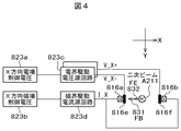
ここで、直交電磁偏向器(ExB)822が一次ビーム・二次ビームに対する分離・偏向作用は、図3、図4、図5に用いて説明する。直交電磁偏向器(ExB)は一般的に図3に示すようにX、Y方向にそれぞれ配置して、二次ビームを任意の方向へ偏向できる。なお、図4と図5の説明では簡略化のため、X方向の電磁偏向器と電界偏向器およびそれぞれの制御回路のみを図示し、Y方向は省略している。図4は直交電磁偏向器と二次ビームA211の俯瞰図である。図5は直交電磁偏向器と一次ビームA21の俯瞰図である。 Here, the separation / deflection action of the orthogonal electromagnetic deflector (ExB) 822 on the primary beam and the secondary beam will be described with reference to FIGS. 3, 4, and 5. The orthogonal electromagnetic deflector (ExB) is generally arranged in the X and Y directions as shown in FIG. 3 to deflect the secondary beam in an arbitrary direction. 4 and 5, only the electromagnetic deflector and the electric field deflector in the X direction and their respective control circuits are shown for simplification, and the Y direction is omitted. FIG. 4 is an overhead view of the orthogonal electromagnetic deflector and the secondary beam A211. FIG. 5 is an overhead view of the orthogonal electromagnetic deflector and the primary beam A21.
直交電磁偏向器の電界偏向器の電極816eと対向電極816fとの間に±Vx(V)の電位差を与えて電界Eを発生させると、加速電圧Vaccの一次電子線A21は、発生する電界Eと同一方向に偏向する力を受けて、Ve/Vaccに比例した角度θe=Ke・Ve/Vaccだけ偏向される。ここで、Veは、電界偏向器の電極間電圧であり、Keは電極816eおよび対向電極816fの形状や配置で決まる定数である。
When the electric field E is generated by applying a potential difference of ± Vx (V) between the
一方、直交磁界発生コイル816a、816bに励磁電流Ix(A)を流すと電界Eと直交する磁界Bが発生し、一次電子線A21はIx/√Vaccに比例した角度θb=Kb・Ix/√Vaccだけ電界による偏向とは逆向きに偏向される。ここで、Kbは、直交磁界発生コイル816a、816bの形状や配置で決まる定数である。互いに直交する電界Eと磁界Bが同時に存在する場合には、電界Eと磁界Bによる力の合成で一次電子線の軌道が決まるため、θe=θbに選べば一次電子線は偏向作用を受けずに直進する。
On the other hand, when an exciting current Ix (A) is passed through the orthogonal magnetic
一方、試料810から発生した二次電子(又は、反射電子)A211は、一次電子A21と進行方向が逆向きであるため、電界と磁界とで同一方向、即ち、電極側に偏向される。偏向する角度は、二次電子(又は、反射電子)A211のエネルギーに依存する。一次電子が偏向されない条件:θe=θb、電圧Vxと電流Ibとの関係をVx=K・Vacc、Ix=K・(Ke/Kb)・√Vaccとすればよい。ここで、Kは、二次電子や反射電子の偏向角度を決める定数である。Vaccが一定であれば、Vx=Kx・Ixの形に書き換えられる。この関係を満たす条件を、以下に「ウイン(Wien)条件」と呼ぶ。
このウイン条件は、直交電磁偏向器が発生した電界と磁界が一次ビームへの影響を打ち消す条件である。Kxは直交電磁偏向器の電極形状や配置、コイルの状や配置、一次ビームの加速速度に依存する。
On the other hand, the secondary electrons (or reflected electrons) A211 generated from the
This Win condition is a condition in which the electric field and magnetic field generated by the orthogonal electromagnetic deflector cancel the influence on the primary beam. Kx depends on the electrode shape and arrangement of the orthogonal electromagnetic deflector, the coil shape and arrangement, and the acceleration speed of the primary beam.
図3に示すように直交電磁偏向器がX、Y方向にそれぞれ配置して、二次ビームを任意の方向へ偏向できる場合は、ウイン条件は同じ方向の電界制御電圧と磁界制御電流間の関係以外、X方向の電圧とY方向の電流の間にも下記(式1)及び(式2)で示す制約条件ある。 As shown in FIG. 3, when the orthogonal electromagnetic deflectors are arranged in the X and Y directions, respectively, and the secondary beam can be deflected in any direction, the win condition is the relationship between the electric field control voltage and the magnetic field control current in the same direction. Other than these, there are also constraint conditions shown in the following (Expression 1) and (Expression 2) between the voltage in the X direction and the current in the Y direction.
(式1):Vx=K1・Ix+K2・Iy
(式2):Vy=K3・Ix+K4・Iy
これはX方向の電極、コイルとY方向の電極、コイルの製造・実装誤差に起因する。
ここで、上記式中のK1、K2、K3、K4は以下の関係を満足する。すなわち、
・K1>>K2、且つK1>>K3、且つK4>>K2、且つK4>>K3
K1、K2、K3、K4は電極、コイルの製造・実装誤差に依存するから、装置に実装した後、最初に調整が必要である。
(Formula 1): Vx = K1 · Ix + K2 · Iy
(Formula 2): Vy = K3 · Ix + K4 · Iy
This is due to manufacturing / mounting errors of the X-direction electrode, the coil and the Y-direction electrode, and the coil.
Here, K1, K2, K3, and K4 in the above formula satisfy the following relationship. That is,
K1 >> K2 and K1 >> K3 and K4 >> K2 and K4 >> K3
Since K1, K2, K3, and K4 depend on the manufacturing and mounting errors of the electrodes and coils, adjustment is necessary first after mounting in the apparatus.
・電界により偏向量が加速電圧Vaccに反比例、磁界により偏向量が加速電圧Vaccのルートに反比例ので、一次ビームの加速電圧Vaccに応じてK1、K2、K3、K4の調整が必要である。 Since the deflection amount is inversely proportional to the acceleration voltage Vacc by the electric field and the deflection amount is inversely proportional to the route of the acceleration voltage Vacc by the magnetic field, adjustment of K1, K2, K3, and K4 is required according to the acceleration voltage Vacc of the primary beam.
そのため、従来の装置では、電界を制御する電圧の値と磁界を制御する電流の値との関係を任意に調整できるように、発生回路が別々に独立していることが特徴である。 Therefore, the conventional apparatus is characterized in that the generation circuits are separately provided so that the relationship between the voltage value for controlling the electric field and the current value for controlling the magnetic field can be arbitrarily adjusted.
ところで、電界偏向器を制御する電圧源回路と磁界偏向器を制御電流源回路において、回路構成素子で発生した回路ノイズが一次電子ビームの走査位置ずれを発生させることになる。 By the way, in the voltage source circuit for controlling the electric field deflector and the magnetic current deflector in the control current source circuit, the circuit noise generated in the circuit constituent element causes the scanning position shift of the primary electron beam.
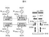
直交電磁偏向器の制御回路のノイズと一次電子ビームの走査ずれの関係について、図6、図7を用いて説明する。図6、図7では一段直交電磁偏向器のX方向を用いて説明するが、偏向器制御回路のノイズと一次電子ビームの走査ずれの関係については、多段直交電磁偏向器やX方向を用いた構成に限られるものではない。 The relationship between the noise of the control circuit of the orthogonal electromagnetic deflector and the scanning deviation of the primary electron beam will be described with reference to FIGS. 6 and 7, the X direction of the single-stage orthogonal electromagnetic deflector will be described. However, regarding the relationship between the noise of the deflector control circuit and the scanning deviation of the primary electron beam, the multi-stage orthogonal electromagnetic deflector and the X direction are used. It is not limited to the configuration.
図6に示す直交電磁偏向器において、試料(ウェハ)上の電子ビーム偏向量Lexは、電界により一次電子ビーム偏向感度がS_exであれば、以下の簡略式(式3)で与えられる。 In the orthogonal electromagnetic deflector shown in FIG. 6, the electron beam deflection amount Lex on the sample (wafer) is given by the following simplified formula (formula 3) if the primary electron beam deflection sensitivity is S_ex by an electric field.
(式3):Lex=Vx・S_ex
磁界により一次電子ビーム偏向量Lbxは、以下の簡略式(式4)で与えられる。
(Formula 3): Lex = Vx · S_ex
The primary electron beam deflection amount Lbx by the magnetic field is given by the following simplified formula (Formula 4).
(式4):Lbx=Ix・S_bx
となる。
(Formula 4): Lbx = Ix · S_bx
It becomes.
ウイン条件を満足するVxとIxであれば、
Vx=K1・Ix、 K1・S_ex=S_bx
Lex=Lbx、偏向方向逆であり、一次電子ビームの走査ずれはない。
If Vx and Ix satisfy the win conditions,
Vx = K1 · Ix, K1 · S_ex = S_bx
Lex = Lbx, the deflection direction is reversed, and there is no scanning deviation of the primary electron beam.
一方、直交電磁偏向器の制御回路の回路ブロックに回路ノイズが存在すると、回路ノイズにより発生する電界と磁界の方向・大きさは、ウイン条件に満足できず、一次電子ビームの走査ずれは発生する。 On the other hand, if circuit noise exists in the circuit block of the control circuit of the orthogonal electromagnetic deflector, the direction and magnitude of the electric field and magnetic field generated by the circuit noise cannot satisfy the WIN condition, and scanning deviation of the primary electron beam occurs. .
例えば、図6、図7示すように、X方向電場制御電圧のノイズ823eがN_ECV_X、電界駆動電圧源回路のノイズ823fがN_EAmpV_Xであり、これらのランダム性ノイズに起因する一次電子ビームのずれ量は、
(式5):L_ENX=((N_ECV_X×GE1+N_EAmpV_X×GE2)×S_ex
の式で表される。
For example, as shown in FIGS. 6 and 7, the
(Expression 5): L_ENX = (( N_ECV_X * GE1 + N_EAmpV_X * GE2) * S_ex
It is expressed by the formula
同じく、X方向磁場制御電圧のノイズ823gがN_BCV_X、磁界駆動電流源回路のノイズ823hがN_BAmpI_Xであり、これらのノイズに起因する一次電子ビームのずれ量は、
(式6):L_BNX=((N_BCV_X×GB1+N_BAmpI_X×GB2)×S_bx
の式で表される。
Similarly,
(Expression 6): L_BNX = (( N_BCV_X * GB1 + N_BAmpI_X * GB2) * S_bx
It is expressed by the formula
ウイン条件に満足すれば、
GE1/GB1=GE2/GB2=K1、K1・S_ex=S_bx
の関係を満たす。
If you are satisfied with the win conditions,
GE1 / GB1 = GE2 / GB2 = K1, K1 · S_ex = S_bx
Satisfy the relationship.
直交電磁偏向器に起因する一次電子ビームのずれ量は、
(式7):L_EXBNX=((N_ECV_X − N_BCV_X)×GB1+(N_EAmpV_X − N_BCV_X)×GB2)×S_bx
の式で表される。
The amount of primary electron beam deviation caused by the orthogonal electromagnetic deflector is
(Equation 7): L _EXBNX = (( N _ECV_X - N _BCV_X) × GB1 + (N _EAmpV_X - N _BCV_X) × GB2) × S_bx
It is expressed by the formula
電界制御電圧のノイズN_ECV_Xと磁界制御電圧のノイズN_BCV_Xは同相であれば打ち消しできるが、これらのノイズがランダム性であるので、発生する一次電子ビームずれ量の大きさは、以下の(式8)の実効値で表わされる。 The noise N _BCV_X noise N _ECV_X and magnetic field control voltage of the field-control voltage Dekiru cancel if phase, since these noises are random, the primary electron beam shift amount generated magnitude, following (formula It is expressed by the effective value of 8).
(式8) δL_EXBNX=((N_ECV_X 2+N_BCV_X 2)×GB12+
(N_EAmpV_X 2+N_BAmpI_X 2)×GB22)(0.5)×S_bx
となる。
上述したことから、直交電磁偏向器の制御回路のノイズにおいて、電界偏向器と磁界偏向器における無相関なノイズ成分が電子ビームの走査ずれの主要因である。
(Formula 8) δL — EXBNX = ((N — ECV — X 2 + N — BCV — X 2 ) × GB1 2 +
( N_EAmpV_X 2 + N_BAmpI_X 2 ) × GB 2 2 ) (0.5) × S_bx
It becomes.
From the above, in the noise of the control circuit of the orthogonal electromagnetic deflector, an uncorrelated noise component in the electric field deflector and the magnetic field deflector is the main factor of the scanning deviation of the electron beam.
従って、電子ビームの走査ずれを低減するために、電界偏向器と磁界偏向器に印加する非無相関な回路ノイズを低減すること、及び電界偏向器と磁界偏向器に対して偏向制御回路の共通化を図ることが必要となる。 Accordingly, in order to reduce scanning deviation of the electron beam, non-correlated circuit noise applied to the electric field deflector and the magnetic field deflector is reduced, and a common deflection control circuit is used for the electric field deflector and the magnetic field deflector. It is necessary to make it easier.
以下の実施例においては、直交電磁偏向器に用いた一次ビーム・二次ビーム分離手段について、電界によって二次電子を検出器側に偏向すると共に、この電界の一次電子線への影響を相殺し、且つ二次電子を検出器側に導くように電界と直交する方向に磁界を発生させる構成ことについて説明する。 In the following embodiments, for the primary beam / secondary beam separating means used in the orthogonal electromagnetic deflector, the secondary electrons are deflected to the detector side by the electric field, and the influence of the electric field on the primary electron beam is canceled out. A configuration for generating a magnetic field in a direction orthogonal to the electric field so as to guide secondary electrons to the detector side will be described.
本実施例においては、直交電磁偏向器に用いた一次ビーム・二次ビーム分離手段について、電界偏向器を制御する電圧源回路と磁界偏向器を制御する電流源制御回路の制御信号生成部を共通化する構成と、磁界を制御する電流信号に基準として電界を制御する電圧信号がウイン条件に満足するように調整する構成について説明する。 In this embodiment, for the primary beam / secondary beam separation means used in the orthogonal electromagnetic deflector, the control signal generator of the voltage source circuit for controlling the electric field deflector and the current source control circuit for controlling the magnetic field deflector are shared. And a configuration for adjusting the voltage signal for controlling the electric field based on the current signal for controlling the magnetic field to satisfy the Win condition will be described.
本実施例における走査型電子ビーム方式の計測検査装置は、図8で説明した従来の走査型電子ビーム方式の計測検査装置の構成のうち、直交電磁偏向器において、電界偏向器と磁界偏向器を制御する直交電磁偏向器の制御回路の構成を、図1に示したような構成と置き換えたものである。従って、以下では、図1、8を用いて説明する。 The scanning electron beam type measurement / inspection apparatus in the present embodiment includes an electric field deflector and a magnetic field deflector in the orthogonal electromagnetic deflector of the configuration of the conventional scanning electron beam type measurement / inspection apparatus described in FIG. The configuration of the control circuit of the orthogonal electromagnetic deflector to be controlled is replaced with the configuration as shown in FIG. Therefore, the following description will be made with reference to FIGS.
直交電磁偏向器においては、二次電子・反射電子を検出器への方向へ偏向するため、直交する2方向(X方向とY方向)への偏向を互いに独立の制御するために、通常最低X、Y方向それぞれの偏向電極と偏向コイルが必要である。 In the quadrature electromagnetic deflector, secondary electrons and reflected electrons are deflected in the direction toward the detector. Therefore, in order to control the deflection in two orthogonal directions (X direction and Y direction) independently from each other, the minimum X , Y direction deflection electrodes and deflection coils are required.
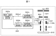
説明を簡略するため、図1では、X方向のみの電界偏向器と磁界偏向器およびそれらの電圧と電流制御回路のブロックをしか表示していない。Y方向の構成は本実施例と同じである。 For the sake of simplicity, FIG. 1 shows only the electric field deflector and magnetic field deflector only in the X direction, and their voltage and current control circuit blocks. The configuration in the Y direction is the same as in this embodiment.
本実施例における走査型電子ビーム方式の計測検査装置の動作を図8に示した装置構成を用いて説明すると、鏡筒830の内部(真空)において、電子銃801より生成・射出された電子ビームA21は、第1コンデンサレンズ(集束レンズ)802、絞り803、第2コンデンサレンズ(集束レンズ)804を通じて集束され、偏向電極808により形成された電界中を進んで偏向電極808に印加される偏向電圧に応じて電子ビームは走査偏向制御が行われ、対物レンズ809等を経て試料810上を走査しながら照射される。ビームA24が照射されると、試料810からは二次電子A211が発生し、直交電磁偏向器816の電界と磁界により二次電子A211は偏向されて検出器807で検出される。検出器807で検出された信号(アナログ信号)は、信号検出部827(二次電子信号検出回路)によってデジタル信号に変換される。そしてそのデジタル信号をもとに画像処理部)828(二次電子信号処理回路)で二次元の画像が生成処理され、GUI部826の画面に表示される。この画像内に基づいて回路パターンが計測される(計測機能の場合)。
The operation of the scanning electron beam type measurement / inspection apparatus according to the present embodiment will be described with reference to the apparatus configuration shown in FIG. 8. The electron beam generated and emitted from the
次に、図1、8を用いて、本実施例の電界偏向器と磁界偏向器を制御する直交電磁偏向器の制御回路の構成を説明する。 Next, the configuration of the control circuit of the orthogonal electromagnetic deflector that controls the electric field deflector and the magnetic field deflector according to the present embodiment will be described with reference to FIGS.
一次電子ビームA21の照射で試料810から発生した二次電子(あるいは、反射電子)A211は、直交電磁偏向器816を構成する磁界偏向器116a、116bと電界偏向器116e、116fからの力を受けて検出器807の方向に偏向され、検出される。検出される二次ビーム(二次電子・反射電子)A211の偏向角度は、直交電磁偏向器816が発生した電界・磁界の強さと比例して、二次ビームA211のエネルギーと反比例する。試料からの二次電子や反射電子のエネルギーが異なって、実装位置が固定された検出器に入射するため、直交電磁偏向器816が発生した電界・磁界の大きさを直交電磁偏向器の制御回路302の出力電圧・出力電流を制御する。
Secondary electrons (or backscattered electrons) A211 generated from the
一方、直交電磁偏向器816が発生した電界・磁界は一次電子ビームA21の走査位置を影響しないように、電界を制御する電圧源回路の出力電圧Vxと磁界を制御する電流源回路の出力電流のIxはウイン条件を満足する。
On the other hand, the output voltage Vx of the voltage source circuit that controls the electric field and the output current of the current source circuit that controls the magnetic field are controlled so that the electric field / magnetic field generated by the orthogonal
直交電磁偏向器の制御回路302は、電界・磁界共通電圧発生部302aから二次ビームA211のエネルギーに応じた二次ビームの偏向角度を決定する電圧値302a1を生成する。生成した電圧値を磁界駆動電流源回路302cで磁界を制御する電流へ変換・増幅して、磁界偏向器116a、116bへ印加する。一方、電圧値302a1をゲイン調整手段302bで電界を制御する電圧源回路の出力電圧Vxと磁界を制御する電流源回路の出力電流のIxはウイン条件を満足するように調整して、電界駆動電圧源回路302cで電界を制御する電圧へ増幅して、電界偏向器116e、116fへ印加する。
The
このような構成で、従来の装置構成で一次電子ビームA21の位置ずれを生じる直交電磁偏向器の制御回路ノイズの主要部分が、電界制御回路と磁界制御回路に対して共通化した同相成分になって、この部分のノイズに起因する電界と磁界の揺れ方向が逆方向で、大きさはウイン条件に満足する。さらに、電圧源制御信号の周波数特性および位相特性と電流源制御信号の周波数特性および位相特性と一致する。 With such a configuration, the main part of the control circuit noise of the orthogonal electromagnetic deflector that causes the positional deviation of the primary electron beam A21 in the conventional apparatus configuration is an in-phase component common to the electric field control circuit and the magnetic field control circuit. Thus, the electric field and the magnetic field caused by the noise in this part are in opposite directions, and the magnitude satisfies the WIN condition. Furthermore, the frequency characteristics and phase characteristics of the voltage source control signal coincide with the frequency characteristics and phase characteristics of the current source control signal.
よって、電磁偏向器制御回路の共通化回路ノイズに起因する一次電子ビームへの偏向力について、電界偏向器と磁界偏向器のノイズ部分は打ち消すことができ、一次電子ビームの位置ずれを低減できる。 Therefore, with respect to the deflection force to the primary electron beam caused by the common circuit noise of the electromagnetic deflector control circuit, the noise portion of the electric field deflector and the magnetic field deflector can be canceled, and the displacement of the primary electron beam can be reduced.
以上、本実施例によれば、走査型電子ビーム方式の半導体(試料)の計測検査装置及び方法において、一次・二次電子を分離する手段の高電圧・大電流実現すると共に、一次ビームへの揺れ影響を最小限に抑制でき、分解能とスループットの向上を図ることができる。 As described above, according to the present embodiment, in the scanning electron beam type semiconductor (sample) measurement / inspection apparatus and method, the means for separating the primary and secondary electrons can be realized with a high voltage and a large current, and can be applied to the primary beam. The influence of shaking can be suppressed to the minimum, and the resolution and throughput can be improved.
図2を用いて、本発明の実施例2の走査型電子ビーム方式の計測検査装置、及びそれを用いた計測検査方法について、従来例と比較しながら説明する。 A scanning electron beam type measurement / inspection apparatus according to Example 2 of the present invention and a measurement / inspection method using the same will be described with reference to FIG.
本実施例では、一次・二次電子を分離して二次ビームを偏向する直交電磁偏向器が2段以上構成された手段を提供する。なお、図2では2段構成の場合を図示している。
この2段構成二次ビーム偏向手段の特徴は、1段構成の二次ビーム偏向手段により一次電子ビームの色収差問題を解決できる点にある。
In the present embodiment, there is provided means in which two or more orthogonal electromagnetic deflectors for separating the primary and secondary electrons and deflecting the secondary beam are configured. FIG. 2 shows a case of a two-stage configuration.
The feature of this two-stage secondary beam deflecting means is that the primary electron beam chromatic aberration problem can be solved by the one-stage secondary beam deflecting means.
以下に、実施例2における構成と色収差の補正作用について説明する。
[計測検査装置(システム)]
本実施例2における計測検査装置を含んで成るシステム全体の構成を図2に示す。実施例2における計測検査装置1は、対象の半導体ウェハ(試料110)の自動計測および自動検査を可能とする適用例である。本計測検査装置1は、半導体ウェハ(試料110)の回路パターンにおける寸法値を計測する計測機能、及び同パターンにおける欠陥(異常や不良)を検出する検査機能を備える。
The configuration and the chromatic aberration correcting action in Example 2 will be described below.
[Measurement and inspection equipment (system)]
FIG. 2 shows the configuration of the entire system including the measurement / inspection apparatus according to the second embodiment. The measurement / inspection apparatus 1 according to the second embodiment is an application example that enables automatic measurement and inspection of a target semiconductor wafer (sample 110). The measurement and inspection apparatus 1 includes a measurement function for measuring a dimension value in a circuit pattern of a semiconductor wafer (sample 110) and an inspection function for detecting a defect (abnormality or defect) in the pattern.
本計測検査装置(システム)1は、大きくは、走査型電子顕微鏡100と、信号処理・制御用のコンピュータ200で構成されている。
The measurement and inspection apparatus (system) 1 is mainly composed of a
走査型電子顕微鏡100は、カラム150と試料室130とを備え、試料室130の内部には、測定・検査の対象物である試料110を載置する試料台(ステージ)112、及びこの試料台を駆動するモータ131が設置されている。
The
走査型電子顕微鏡100のカラム150内(真空)には、照射系(電子光学系)として、電子ビームA1を射出する電子銃101、射出された電子ビームA1が通る集束レンズ(第1コンデンサレンズ)102、絞り103、集束レンズ(第2コンデンサレンズ)104、ブランキング(BLK)制御電極105、アパーチャ106、偏向器(電極)120、対物レンズ109等を有する。
In the column 150 (vacuum) of the
また、カラム150は検出系として、照射された電子ビームA1(A4)により試料110から発生した二次電子・反射電子A11を検出する検出器107、およびA11を検出器107の方向へ偏向する二次電子・反射電子直交電磁偏向器160を備える。偏向器170は偏向器160により発生した一次電子ビームA1(A4)の色収差を補正する直交電磁偏向器である。ここで、電子ビームA1、A4(図示せず)はそれぞれ図8で示したA21、A24に相当する。
The column 150 serves as a detection system. The
コンピュータ200は、例えば制御ラックにPCや制御ボードなどの形態で格納される構成である。コンピュータ200の各部は、例えばプロセッサ及びメモリ等によるソフトウェアプログラム処理、あるいは専用回路の処理などで実現される。
The
コンピュータ200には、全体制御部210と、ブランキング(BLK)制御回路201と、電子ビームの位置シフトと偏向走査とを制御するイメージシフト・偏向制御回路206と、機構系制御部230と、信号検出部(二次電子信号検出回路)207と、画像処理部(二次電子信号処理回路)208と、GUI部(ユーザインタフェース部)250、等を備える。
The
走査型電子顕微鏡100のカラム150内(真空)において、電子銃101より生成・射出された電子ビームA1は、第1コンデンサレンズ(集束レンズ)102、絞り103、第2コンデンサレンズ(集束レンズ)104を通じて集束され、イメージシフトと走査一体化された偏向器120を介してビームの照射中心に移動と走査偏向制御され、対物レンズ109等を経て試料110上を走査しながら照射される。ビームA1(A4)が照射されると、試料110からは二次電子A11が発生し、検出器107で検出される。検出器107で検出された信号(アナログ信号)は、信号検出部207(二次電子信号検出回路)によってデジタル信号に変換される。そしてそのデジタル信号をもとに画像処理部208(二次電子信号処理回路)で二次元の画像が生成処理され、GUI画面で表示される。この画像内に基づいて回路パターンが計測される(計測機能の場合)。
In the column 150 (vacuum) of the
GUI部250は、ユーザ(測定・検査者)に対するインタフェース(GUI画面など)を提供する処理を行う。GUI部250では、検査条件などを入力(設定)するGUI画面や、検査結果(二次元の画像など)を表示するGUI画面などを提供する。GUI部250は、キーボードやディスプレイ等の入出力装置や通信インタフェース部などを含む。ユーザは、GUI画面で計測機能や検査機能を選択実行可能である。
The
全体制御部210は、GUI部250での指示に従い、本システム(装置)の全体(電子光学制御部220、機構系制御部230、イメージシフト・偏向制御回路206、信号検出部207、画像処理部208、ステージ位置検出部等)を制御する処理を行う。例えば全体制御部210は、GUI部250の画面でユーザにより入力された計測・検査条件や指示などに応じて、電子光学制御部220、イメージシフト・偏向制御回路206、機構系制御部230などを制御することで、計測の処理を行う。例えば全体制御部210は、計測の実行時、信号処理部207及び画像処理部208を通じて生成された二次元の画像などのデータ情報を受信し、GUI部250の画面で表示させる。
The
電子光学制御部220は、全体制御部210からの制御に従い、カラム100内の電子銃101、第1コンデンサレンズ(集束レンズ)102、絞り103、第2コンデンサレンズ(集束レンズ)104、ブランキング制御電極105、対物レンズ109等の電子光学系(照射系)を制御する。ブランキング制御回路201は、信号ラインを介してブランキング制御電極105を制御して、電子ビームA1の試料110への照射を停止するときには、電子ビームA1の軌道を曲げて電子ビームA1をアパーチャ106に照射させる。
The electron
イメージシフト・偏向制御回路206は、全体制御部210からの制御に従い、偏向器120に対して信号ライン(c1、c2)を通じて偏向制御信号を印加することにより、電子ビームの位置をシフトさせると共にこのシフトした位置における偏向による走査を制御する。
The image shift /
2段直交電磁偏向器303の制御部は、全体制御部210からの制御に従い、一次ビーム・二次ビーム分離する直交電磁偏向器160に対して信号ライン(b1)を通じて二次ビーム偏向制御信号を印加することにより、二次電子・反射電子を検出器107の方向へ偏向させると共に、一次電子ビームの走査方向に影響を与えないような制御をする。
The control unit of the two-stage orthogonal
しかしながら、このような直交電磁界発生器は、ウィンフィルターエネルギー分光器と同等の作用により、一次電子線をエネルギー分散させることになるため、大きな偏向力の発生により、色収差の問題が大きくなる。そのため、2段直交電磁偏向器制御部303は、全体制御部210からの制御に従い、直交電磁偏向器170に対して信号ライン(b2)を通じて一次電子ビーム色収差補正制御信号を印加することにより、直交電磁偏向器160が二次ビームを大きく偏向すると同時に生じた一次電子ビームの色収差を、逆電界と磁界の生成により補正を制御する。
However, such an orthogonal electromagnetic field generator disperses the energy of the primary electron beam by an action equivalent to that of the Win filter energy spectrometer, so that the problem of chromatic aberration increases due to the generation of a large deflection force. Therefore, the two-stage orthogonal electromagnetic
図9は、本発明の実施例2に係る2段直交電磁偏向器303とその制御回路の構成を示すブロック図である。
図9に示すように、2段直交電磁偏向器の上段偏向器170を制御する部分と下段偏向器160を制御する部分で構成する。一次電子ビームへの位置ずれ影響を最小限するために、各段制御回路の構成は実施例1で説明した構成と同じであり、電圧源回路と電流源回路の信号発生部を共通化する。
FIG. 9 is a block diagram showing the configuration of a two-stage orthogonal
As shown in FIG. 9, it comprises a part for controlling the
さらに、電圧源制御信号およびと電流源制御信号のそれぞれの周波数特性および位相特性を一致させる。よって、各段電磁偏向器制御回路の共通化回路ノイズに起因する一次電子ビームへの偏向力について、電界偏向器と磁界偏向器の部分は打ち消しができ、一次電子ビームの位置ずれを低減できる。 Further, the frequency characteristics and the phase characteristics of the voltage source control signal and the current source control signal are matched. Therefore, the electric field deflector and the magnetic field deflector can be canceled out with respect to the deflecting force to the primary electron beam caused by the common circuit noise of each stage electromagnetic deflector control circuit, and the displacement of the primary electron beam can be reduced.
なお、周波数特性および位相特性を一致させる手段の一例としては、電圧源回路と電流源回路の周波数帯域や減衰特性が同じようになるように、それぞれの出力段にフィルタを設けることで、共通制御信号部で発生するノイズの位相・周波数特性を一致させることができる。 As an example of means for matching the frequency characteristics and phase characteristics, a common control can be performed by providing a filter in each output stage so that the frequency band and attenuation characteristics of the voltage source circuit and current source circuit are the same. The phase / frequency characteristics of noise generated in the signal section can be matched.
図2において、機構系制御部230は、試料室130に設置された試料台112を駆動するモータ131等を含む機構系を制御する。例えば、電子ビームの走査制御に対応させてモータ131を駆動して、試料台112を移動制御することが可能である。このとき、モータ131の回転信号はステージ位置検出部(図示せず)に送られて、試料台112の位置情報が得られる。
In FIG. 2, the mechanism
なお、図2のコンピュータ200(全体制御部210等)において、計測機能と検査機能の両方を備えるが、一方のみ備える形態としてもよい。画像処理部208は、計測時(計測機能)の場合は、計測画像を生成し、当該画像内のパターン寸法値の計算などを行い、また、検査時(検査機能)の場合は、検査画像を生成し、当該画像内の欠陥を検出・判定する処理などを行う。
In addition, although the computer 200 (
本実施例によれば、走査型電子ビーム方式の半導体(試料)の計測検査装置及び方法などに関して、スループットと計測精度の向上を実現するため、一次ビーム・二次ビーム分離手段として、2段構成の直交電磁偏向器で構成する。一次・二次電子を分離する手段の高電圧・大電流実現すると共に、一次ビームへの揺れ影響と収差を最小限に抑制でき、分解能とスループットの向上を図ることができる。 According to the present embodiment, with respect to a scanning electron beam type semiconductor (sample) measurement / inspection apparatus and method, a two-stage configuration as a primary beam / secondary beam separation means in order to improve throughput and measurement accuracy. The orthogonal electromagnetic deflector is used. The high voltage and large current of the means for separating the primary and secondary electrons can be realized, and the influence and aberration on the primary beam can be suppressed to the minimum, and the resolution and throughput can be improved.
実施例1で説明した構成では、直交電磁偏向器のX方向(或いはY方向)しか示していないが、本実施例における走査型電子ビーム方式の計測検査装置の構成は、直交電磁偏向器と制御回路をX、Y両方向に設ける。 In the configuration described in the first embodiment, only the X direction (or Y direction) of the orthogonal electromagnetic deflector is shown. However, the configuration of the scanning electron beam measurement / inspection apparatus in this embodiment is similar to that of the orthogonal electromagnetic deflector and the control. Circuits are provided in both X and Y directions.
図10は、本発明の実施例3に係る直交電磁偏向器の制御回路の構成を示すブロック図である。本図に示すように、実施例1で説明した直交電磁偏向器の制御回路は、X、Y両方向の直交電磁偏向きの電界・磁界を制御する電圧源回路と電流源回路から構成される。各方向において、一次電子ビームへの位置ずれ影響を最小限にするために、電圧源回路と電流源回路の信号発生部を共通化する。さらに、電圧源制御信号の周波数特性および位相特性と、電流源制御信号の周波数特性および位相特性とが一致する。よって、各方向に対する直交電磁偏向器制御回路の共通化回路ノイズに起因する一次電子ビームへの偏向力について、電界偏向器と磁界偏向器の部分は打ち消しができ、一次電子ビームの位置ずれを低減できる。 FIG. 10 is a block diagram showing the configuration of the control circuit of the orthogonal electromagnetic deflector according to the third embodiment of the present invention. As shown in this figure, the control circuit for the orthogonal electromagnetic deflector described in the first embodiment is composed of a voltage source circuit and a current source circuit for controlling the electric field and magnetic field of the orthogonal electromagnetic deflection in both the X and Y directions. In each direction, the signal generator of the voltage source circuit and the current source circuit is shared in order to minimize the influence of the position shift on the primary electron beam. Further, the frequency characteristic and phase characteristic of the voltage source control signal are matched with the frequency characteristic and phase characteristic of the current source control signal. Therefore, the electric field deflector and magnetic field deflector can cancel out the deflection force to the primary electron beam caused by the common circuit noise of the orthogonal electromagnetic deflector control circuit for each direction, and the displacement of the primary electron beam is reduced. it can.
本実施例によれば、走査型電子ビーム方式の半導体(試料)の計測検査装置及び方法などに関して、スループットと計測精度の向上を実現するため、一次ビーム・二次ビーム分離手段として、X、Y方向のそれぞれを直交電磁偏向器で構成する。一次・二次電子を分離する手段の高電圧・大電流実現すると共に、一次ビームへの揺れ影響と収差を最小限に抑制でき、分解能とスループットの向上を図ることができる。 According to the present embodiment, with respect to a scanning electron beam type semiconductor (sample) measurement / inspection apparatus and method, in order to realize improvement in throughput and measurement accuracy, X, Y can be used as primary beam / secondary beam separation means. Each of the directions is composed of orthogonal electromagnetic deflectors. The high voltage and large current of the means for separating the primary and secondary electrons can be realized, and the influence and aberration on the primary beam can be suppressed to the minimum, and the resolution and throughput can be improved.
実施例3で説明した構成では、直交電磁偏向器と制御回路をX、Y両方向に設けるが、
各方向の制御電圧と制御電流の制御は独立して行うことが特徴である。
In the configuration described in the third embodiment, the orthogonal electromagnetic deflector and the control circuit are provided in both the X and Y directions.
The control voltage and control current in each direction are controlled independently.
本実施例における走査型電子ビーム方式の計測検査装置の構成では、直交電磁偏向器と制御回路をX、Y両方向に設けている。且つ、X、Y両方向の制御電圧と制御電流の制御は、独立ではないことが特徴である。これはX方向の電極、コイルとY方向の電極、コイルの製造・実装誤差によって、X、Y方向で独立に発生した電磁界は直交することはないので、回転効果を補正することが必要である。 In the configuration of the scanning electron beam type measurement / inspection apparatus in this embodiment, the orthogonal electromagnetic deflector and the control circuit are provided in both the X and Y directions. In addition, the control voltage and the control current in both X and Y directions are not independent. This is because the electromagnetic fields generated independently in the X and Y directions are not orthogonal to each other due to manufacturing and mounting errors of the X direction electrodes, coils and Y direction electrodes, and coils, so it is necessary to correct the rotation effect. is there.
図11は、本発明の実施例4に係る直交電磁偏向器の制御回路の構成を示すブロック図である。 FIG. 11 is a block diagram illustrating a configuration of a control circuit of the orthogonal electromagnetic deflector according to the fourth embodiment of the present invention.
図11に示すように、直交電磁偏向器の制御回路は、X、Y両方向の直交電磁偏向器の電界・磁界を制御する電圧源回路と電流源回路から構成される。 As shown in FIG. 11, the control circuit for the orthogonal electromagnetic deflector includes a voltage source circuit and a current source circuit for controlling the electric field and magnetic field of the orthogonal electromagnetic deflector in both the X and Y directions.
直交電磁偏向器制御回路305は、X方向用直交電磁偏向器制御部とY方向用電界・磁界直交電磁偏向器制御部から構成される。X方向用の直交電磁偏向器制御部は、X方向電界・磁界共通電圧発生部305aから二次ビームのエネルギーに応じた二次ビームのX方向偏向角度を決定する電圧値305a1を生成する。Y方向用の直交電磁偏向器制御部は、Y方向電界・磁界共通電圧発生部305dから二次ビームのエネルギーに応じた二次ビームのY方向偏向角度を決定する電圧値305d1を生成する。生成したX方向共通電圧値305a1をX方向磁界駆動電流源回路305bでX方向磁界を制御する電流へ変換・増幅して、X方向磁界偏向器へ印加する。生成したY方向共通電圧値305d1をY方向磁界駆動電流源回路305eでY方向磁界を制御する電流へ変換・増幅して、Y方向磁界偏向器へ印加する。
The orthogonal electromagnetic
一方、X方向偏向器とY方向偏向器の回転効果を補正するため、X方向電界を制御する電圧源回路の出力電圧Vxは、X方向共通電圧値305a1とY方向共通電圧値305d1を、それぞれゲイン調整手段305gと305hでの調整結果を加算し、その値を電界駆動電圧源回路305cへ入力し、電界駆動電圧源回路305cで電界を制御する電圧へ増幅してX方向電界偏向器へ印加する。
On the other hand, in order to correct the rotation effect of the X-direction deflector and the Y-direction deflector, the output voltage Vx of the voltage source circuit that controls the X-direction electric field has an X-direction common voltage value 305a1 and a Y-direction common voltage value 305d1, respectively. The adjustment results of the gain adjusting means 305g and 305h are added, and the value is input to the electric field driving
同様に、X方向偏向器とY方向偏向器の回転効果を補正するため、Y方向電界を制御する電圧源回路の出力電圧VyはX方向共通電圧値305a1とY方向共通電圧値305d1を、それぞれゲイン調整手段305iと305jでの調整結果を加算し、その値を電界駆動電圧源回路305fへ入力し、電界駆動電圧源回路305fで電界を制御する電圧へ増幅して、Y方向電界偏向器へ印加する。
Similarly, in order to correct the rotation effect of the X-direction deflector and the Y-direction deflector, the output voltage Vy of the voltage source circuit that controls the Y-direction electric field has an X-direction common voltage value 305a1 and a Y-direction common voltage value 305d1, respectively. The adjustment results of the gain adjusting means 305i and 305j are added, and the value is input to the electric field drive
このような構成で、X、Y方向電磁偏向器の回転効果がある場合にも、一次電子ビームの位置ずれを生じる電磁偏向器制御回路ノイズの主要部分が、電界制御回路と磁界制御回路に対して共通化した同相成分になって、この部分のノイズに起因する電界と磁界の揺れ方向が逆方向で、大きさはウイン条件に満足する。さらに、電圧源制御信号の周波数特性および位相特性と電流源制御信号の周波数特性および位相特性とを一致させる。 With such a configuration, even when there is a rotational effect of the X and Y direction electromagnetic deflectors, the main part of the electromagnetic deflector control circuit noise that causes the positional deviation of the primary electron beam is compared to the electric field control circuit and the magnetic field control circuit. Therefore, the electric field and magnetic field fluctuation directions caused by the noise in this part are opposite directions, and the magnitude satisfies the WIN condition. Further, the frequency characteristic and phase characteristic of the voltage source control signal are matched with the frequency characteristic and phase characteristic of the current source control signal.
本実施例によれば、走査型電子ビーム方式の半導体(試料)の計測検査装置及び方法などに関して、スループットと計測精度の向上を実現するため、一次ビーム・二次ビーム分離手段として、X、Y方向電磁偏向器の回転効果を補正できる直交電磁偏向器で構成する。一次・二次電子を分離する手段の高電圧・大電流実現すると共に、一次ビームへの揺れ影響と収差を最小限に抑制でき、分解能とスループットの向上を図ることができる。 According to the present embodiment, with respect to a scanning electron beam type semiconductor (sample) measurement / inspection apparatus and method, in order to realize improvement in throughput and measurement accuracy, X, Y can be used as primary beam / secondary beam separation means. An orthogonal electromagnetic deflector capable of correcting the rotational effect of the directional electromagnetic deflector is used. The high voltage and large current of the means for separating the primary and secondary electrons can be realized, and the influence and aberration on the primary beam can be suppressed to the minimum, and the resolution and throughput can be improved.
以上、本発明者によってなされた発明を実施の形態に基づき具体的に説明したが、本発明は前記実施の形態に限定されるものではなく、その要旨を逸脱しない範囲で種々変更可能であることは言うまでもない。 As mentioned above, the invention made by the present inventor has been specifically described based on the embodiment. However, the present invention is not limited to the embodiment, and various modifications can be made without departing from the scope of the invention. Needless to say.
上記構成による、本発明の荷電粒子ビーム装置の主な特徴は以下の通りである。
(1) 荷電粒子ビームを生成する荷電粒子銃と、
該荷電粒子銃から放出された荷電粒子ビームをステージに載置した試料上に照射して走査する電子光学系と、
前記試料から発生する二次電子、または反射電子を検出する検出部と、
前記二次電子、または反射電子の進路を前記検出部の方向へ偏向させる直交電磁偏向部と、を有し、
前記直交電磁偏向部は、磁界を発生させて前記荷電粒子ビームの軌跡を変化させる磁界偏向器と、電界を発生させて前記荷電粒子ビームの軌跡を変化させる電界偏向器と、前記磁界偏向器に電流を供給する電流源回路と、前記電界偏向器に電圧を供給する電圧源回路と、前記電流と前記電圧との関係を調整するゲイン調整部と、を備え、
前記磁界偏向器と前記電界偏向器は、前記磁界と前記電界とが互いに直交し重畳するように配置され、
前記電流源回路に電圧を印加する電圧発生部と、前記電圧源回路に電圧を印加する電圧発生部とが一つに共通化され、
前記ゲイン調整部により、前記磁界により進路が偏向される量と前記電界により進路が偏向される量とが一致するように、前記電流と前記電圧との関係が調整される、
ことを特徴とする荷電粒子ビーム装置。
(2) 荷電粒子ビームを生成する荷電粒子銃と、
該荷電粒子銃から放出された荷電粒子ビームをステージに載置した試料上に照射して走査する電子光学系と、
前記試料から発生する二次電子、または反射電子を検出する検出部と、
前記二次電子、または反射電子の進路を前記検出部の方向へ偏向させる直交電磁偏向部と、を有し、
前記直交電磁偏向部は、前記荷電粒子銃から放出される荷電粒子ビームの進路方向に交わる第1の方向に電界および磁界のそれぞれを印加する第1の電界偏向器及び第1の磁界偏向器と、前記第1の方向に直交する第2の方向に電界および磁界のそれぞれを印加する第2の電界偏向器及び第2の磁界偏向器と、前記第1及び第2の磁界偏向器のそれぞれに電流を供給する第1及び第2の電流源回路と、前記第1及び第2の電界偏向器のそれぞれに電圧を供給する第1及び第2の電圧源回路と、前記電流と前記電圧との関係を調整する第1及び第2のゲイン調整部と、をそれぞれ備え、
前記第1及び第2の磁界偏向器は、磁界を発生させて前記荷電粒子ビームの軌跡を変化させ、前記第1及び第2の電界偏向器は、電界を発生させて前記荷電粒子ビームの軌跡を変化させ、
前記第1及び第2の磁界偏向器と前記第1及び第2の電界偏向器は、それぞれの磁界と電界とが互いに直交し重畳するように配置され、
前記第1の電流源回路に電圧を印加する電圧発生部と、前記第1の電圧源回路に電圧を印加する電圧発生部とが一つに共通化された第1の電圧発生部と、
前記第2の電圧源回路に電圧を印加する電圧発生部と、前記第2の電圧源回路に電圧を印加する電圧発生部とが一つに共通化された第2の電圧発生部と、を有し、
前記第1の電圧発生部と前記第2の電圧発生部とは互いに独立して電圧を制御し、
前記第1のゲイン調整部により、前記第1の磁界偏向器により磁界の進路が偏向される量と前記第1の電界偏向器の電界により進路が偏向される量とが一致するように、前記電流と前記電圧との関係が調整され、
前記第2のゲイン調整部により、前記第2の磁界偏向器により磁界の進路が偏向される量と前記第2の電界偏向器の電界により進路が偏向される量とが一致するように、前記電流と前記電圧との関係が調整される、
ことを特徴とする荷電粒子ビーム装置。
The main features of the charged particle beam apparatus of the present invention having the above-described configuration are as follows.
(1) a charged particle gun for generating a charged particle beam;
An electron optical system that irradiates and scans a sample placed on a stage with a charged particle beam emitted from the charged particle gun; and
A detection unit for detecting secondary electrons generated from the sample or reflected electrons;
An orthogonal electromagnetic deflection unit that deflects the path of the secondary electrons or reflected electrons in the direction of the detection unit, and
The orthogonal electromagnetic deflection unit includes a magnetic field deflector that generates a magnetic field to change a locus of the charged particle beam, an electric field deflector that generates an electric field to change the locus of the charged particle beam, and the magnetic field deflector. A current source circuit for supplying a current, a voltage source circuit for supplying a voltage to the electric field deflector, and a gain adjusting unit for adjusting a relationship between the current and the voltage,
The magnetic field deflector and the electric field deflector are arranged so that the magnetic field and the electric field are perpendicular to each other and overlap each other,
A voltage generator that applies a voltage to the current source circuit and a voltage generator that applies a voltage to the voltage source circuit are shared in one,
The gain adjustment unit adjusts the relationship between the current and the voltage so that the amount by which the path is deflected by the magnetic field matches the amount by which the path is deflected by the electric field.
A charged particle beam device characterized by that.
(2) a charged particle gun that generates a charged particle beam;
An electron optical system that irradiates and scans a sample placed on a stage with a charged particle beam emitted from the charged particle gun; and
A detection unit for detecting secondary electrons generated from the sample or reflected electrons;
An orthogonal electromagnetic deflection unit that deflects the path of the secondary electrons or reflected electrons in the direction of the detection unit, and
The orthogonal electromagnetic deflection unit includes a first electric field deflector and a first magnetic field deflector that apply an electric field and a magnetic field, respectively, in a first direction intersecting a path direction of a charged particle beam emitted from the charged particle gun. , A second electric field deflector and a second magnetic field deflector for applying an electric field and a magnetic field in a second direction orthogonal to the first direction, and the first and second magnetic field deflectors, respectively. First and second current source circuits for supplying a current, first and second voltage source circuits for supplying a voltage to each of the first and second electric field deflectors, and the current and the voltage A first and a second gain adjustment unit for adjusting the relationship, respectively,
The first and second magnetic field deflectors generate a magnetic field to change a trajectory of the charged particle beam, and the first and second electric field deflectors generate an electric field to generate a trajectory of the charged particle beam. Change
The first and second magnetic field deflectors and the first and second electric field deflectors are arranged so that respective magnetic fields and electric fields are perpendicular to each other and overlap each other,
A voltage generator that applies a voltage to the first current source circuit and a voltage generator that applies a voltage to the first voltage source circuit;
A voltage generator that applies a voltage to the second voltage source circuit, and a voltage generator that applies a voltage to the second voltage source circuit; Have
The first voltage generation unit and the second voltage generation unit control the voltage independently of each other,
The amount by which the path of the magnetic field is deflected by the first magnetic field deflector and the amount by which the path is deflected by the electric field of the first electric field deflector are matched by the first gain adjusting unit. The relationship between the current and the voltage is adjusted,
The amount by which the path of the magnetic field is deflected by the second magnetic field deflector and the amount by which the path is deflected by the electric field of the second field deflector are matched by the second gain adjusting unit. The relationship between the current and the voltage is adjusted,
A charged particle beam device characterized by that.
1…計測検査装置(システム)、
100…走査型電子顕微鏡(カラム)、
101…電子銃、
102…第1コンデンサレンズ(集束レンズ)、
103…絞り、
104…第2コンデンサレンズ(集束レンズ)、
105…ブランキング(BLK)制御電極、
106…アパーチャ、
107…検出器(二次電子・反射電子検出器)、
109…対物レンズ、
110…試料、
112…試料台(ステージ)、
120…偏向器、
160…直交電磁偏向器、
200…コンピュータ(信号処理系)、
201…ブランキング(BLK)制御回路、
206…イメージシフト・偏向制御回路、
207…信号検出部(二次電子信号検出回路)、
208…画像処理部(二次電子信号処理回路)、
210…全体制御部、
220…電子光学制御部、
230…機構系制御部、
250…GUI部、
303…直交電磁偏向器、
302…直交電磁偏向器の制御回路。
1 ... Measurement inspection device (system),
100: Scanning electron microscope (column),
101 ... an electron gun,
102 ... 1st condenser lens (focusing lens),
103 ... Aperture,
104 ... Second condenser lens (focusing lens),
105 ... Blanking (BLK) control electrode,
106 ... Aperture,
107 ... Detector (secondary electron / reflected electron detector),
109 ... objective lens,
110 ... Sample,
112 ... Sample stage (stage),
120 ... deflector,
160 ... Orthogonal electromagnetic deflector,
200: Computer (signal processing system),
201 ... Blanking (BLK) control circuit,
206: Image shift / deflection control circuit,
207 ... Signal detection unit (secondary electron signal detection circuit),
208: Image processing unit (secondary electron signal processing circuit),
210 ... Overall control unit,
220: Electro-optical control unit,
230 ... mechanical system control unit,
250 ... GUI part,
303 ... Orthogonal electromagnetic deflector,
302: Control circuit for orthogonal electromagnetic deflector.
Claims (3)
該荷電粒子銃から放出された荷電粒子ビームをステージに載置した試料上に照射して走査する電子光学系と、
前記試料から発生する二次電子、または反射電子を検出する検出部と、
前記二次電子、または反射電子の進路を前記検出部の方向へ偏向させる直交電磁偏向部と、を有し、
前記直交電磁偏向部は、前記荷電粒子銃から放出される荷電粒子ビームの進路方向に交わる第1の方向に電界および磁界のそれぞれを印加する第1の電界偏向器及び第1の磁界偏向器と、前記第1の方向に直交する第2の方向に電界および磁界のそれぞれを印加する第2の電界偏向器及び第2の磁界偏向器と、前記第1及び第2の磁界偏向器のそれぞれに電流を供給する第1及び第2の電流源回路と、前記第1及び第2の電界偏向器のそれぞれに電圧を供給する第1及び第2の電圧源回路と、前記電流と前記電圧との関係を調整する第1及び第2のゲイン調整部と、をそれぞれ備え、
前記第1及び第2の磁界偏向器は、磁界を発生させて前記荷電粒子ビームの軌跡を変化させ、前記第1及び第2の電界偏向器は、電界を発生させて前記荷電粒子ビームの軌跡を変化させ、
前記第1及び第2の磁界偏向器と前記第1及び第2の電界偏向器は、それぞれの磁界と電界とが互いに直交し重畳するように配置され、
前記第1の電流源回路に電圧を印加する電圧発生部と、前記第1の電圧源回路に電圧を印加する電圧発生部とが一つに共通化された第1の電圧発生部と、
前記第2の電圧源回路に電圧を印加する電圧発生部と、前記第2の電圧源回路に電圧を印加する電圧発生部とが一つに共通化された第2の電圧発生部と、を有し、
前記第1のゲイン調整部により、前記第1の磁界偏向器により磁界の進路が偏向される量と前記第1の電界偏向器の電界により進路が偏向される量とが一致するように、前記電流と前記電圧との関係が調整され、
前記第2のゲイン調整部により、前記第2の磁界偏向器により磁界の進路が偏向される量と前記第2の電界偏向器の電界により進路が偏向される量とが一致するように、前記電流と前記電圧との関係が調整され
前記第2の電圧発生部から出力される電圧のゲイン調整を行う第3のゲイン調整部と、
前記第1の電圧発生部から出力される電圧のゲイン調整を行う第4のゲイン調整部と、をさらに有し、
前記第1の電圧源回路に、前記第1の電圧発生部から出力される電圧が前記第1のゲイン調整部を介して調整された電圧と、前記第2の電圧発生部から出力される電圧が前記第3のゲイン調整部を介して調整された電圧とが加算された電圧が入力され、
前記第2の電圧源回路に、前記第1の電圧発生部から出力される電圧を前記第4のゲイン調整部を介して調整された電圧と、前記第2の電圧発生部から出力される電圧を前記第2のゲイン調整部を介して調整された電圧とが加算された電圧が入力されることを特徴とする荷電粒子ビーム装置。 A charged particle gun for generating a charged particle beam;
An electron optical system that irradiates and scans a sample placed on a stage with a charged particle beam emitted from the charged particle gun; and
A detection unit for detecting secondary electrons generated from the sample or reflected electrons;
An orthogonal electromagnetic deflection unit that deflects the path of the secondary electrons or reflected electrons in the direction of the detection unit, and
The orthogonal electromagnetic deflection unit includes a first electric field deflector and a first magnetic field deflector that apply an electric field and a magnetic field, respectively, in a first direction intersecting a path direction of a charged particle beam emitted from the charged particle gun. , A second electric field deflector and a second magnetic field deflector for applying an electric field and a magnetic field in a second direction orthogonal to the first direction, and the first and second magnetic field deflectors, respectively. First and second current source circuits for supplying a current, first and second voltage source circuits for supplying a voltage to each of the first and second electric field deflectors, and the current and the voltage A first and a second gain adjustment unit for adjusting the relationship, respectively,
The first and second magnetic field deflectors generate a magnetic field to change a trajectory of the charged particle beam, and the first and second electric field deflectors generate an electric field to generate a trajectory of the charged particle beam. Change
The first and second magnetic field deflectors and the first and second electric field deflectors are arranged so that respective magnetic fields and electric fields are perpendicular to each other and overlap each other,
A voltage generator that applies a voltage to the first current source circuit and a voltage generator that applies a voltage to the first voltage source circuit;
A voltage generator that applies a voltage to the second voltage source circuit, and a voltage generator that applies a voltage to the second voltage source circuit; Have
The amount by which the path of the magnetic field is deflected by the first magnetic field deflector and the amount by which the path is deflected by the electric field of the first electric field deflector are matched by the first gain adjusting unit. The relationship between the current and the voltage is adjusted,
The amount by which the path of the magnetic field is deflected by the second magnetic field deflector and the amount by which the path is deflected by the electric field of the second field deflector are matched by the second gain adjusting unit. A third gain adjustment unit that adjusts a gain of a voltage that is adjusted in a relationship between a current and the voltage and that is output from the second voltage generation unit;
A fourth gain adjustment unit for adjusting the gain of the voltage output from the first voltage generation unit;
The voltage output from the first voltage generator to the first voltage source circuit is adjusted via the first gain adjuster, and the voltage output from the second voltage generator Is inputted with a voltage obtained by adding the voltage adjusted via the third gain adjustment unit,
The voltage output from the first voltage generator to the second voltage source circuit is adjusted via the fourth gain adjuster, and the voltage output from the second voltage generator The charged particle beam device is characterized in that a voltage obtained by adding the voltage adjusted via the second gain adjustment unit is input.
前記第1の電圧源回路からの第1電圧は、前記第1の電流源回路からの第1電流と前記第2の電流源回路からの第2電流とに依存し、
前記第2の電圧源回路からの第2電圧は、前記第1の電流源回路からの第1電流と前記第2の電流源回路からの第2電流とに依存することを特徴とする荷電粒子ビーム装置。 The charged particle beam device according to claim 1 .
A first voltage from the first voltage source circuit depends on a first current from the first current source circuit and a second current from the second current source circuit;
The charged voltage, wherein the second voltage from the second voltage source circuit depends on a first current from the first current source circuit and a second current from the second current source circuit. Beam device.
前記第1及び第2の磁界偏向器、電界偏向器のそれぞれに電流、電圧をそれぞれ供給する第1及び第2の電流源回路と、電圧源回路と、及びゲイン調整部を有する第1と第2制御回路と、
前記第1の電流源回路と電圧源回路に電圧を供給する第1の共通電圧発生部と、
前記第2の電流源回路と前記第2の電圧源回路に電圧を供給する第2の共通電圧発生部と、
前記第1の共通電圧発生部からの電圧の調整する第1及び第2のゲイン調整部と、
前記第2の共通電圧発生部からの電圧の調整する第3及び第4のゲイン調整部と、を有し、
前記第1の制御回路は、前記第1のゲイン調整部と前記第3のゲイン調整部からの電圧を加算する第1の加算回路を有し、
前記第2の制御回路は、前記第2のゲイン調整部と前記第4のゲイン調整部からの電圧を加算する第2の加算回路を有することを特徴とする荷電粒子ビーム装置。 A second-direction electric field deflector and a magnetic field deflector, and a second direction electric field deflector and a magnetic field deflector;
First and second current source circuits that supply current and voltage respectively to the first and second magnetic field deflectors and electric field deflector, a voltage source circuit, and a gain adjusting unit. Two control circuits;
A first common voltage generator for supplying a voltage to the first current source circuit and the voltage source circuit;
A second common voltage generator for supplying a voltage to the second current source circuit and the second voltage source circuit;
First and second gain adjusters for adjusting the voltage from the first common voltage generator;
A third and a fourth gain adjuster for adjusting the voltage from the second common voltage generator,
The first control circuit includes a first addition circuit that adds voltages from the first gain adjustment unit and the third gain adjustment unit,
The charged particle beam apparatus, wherein the second control circuit includes a second addition circuit that adds voltages from the second gain adjustment unit and the fourth gain adjustment unit.
Priority Applications (4)
| Application Number | Priority Date | Filing Date | Title |
|---|---|---|---|
| JP2014002260A JP6254445B2 (en) | 2014-01-09 | 2014-01-09 | Charged particle beam equipment |
| US15/109,230 US9679740B2 (en) | 2014-01-09 | 2014-12-16 | Charged particle beam device |
| PCT/JP2014/083200 WO2015104959A1 (en) | 2014-01-09 | 2014-12-16 | Charged particle beam device |
| US15/613,941 US10424459B2 (en) | 2014-01-09 | 2017-06-05 | Charged particle beam device |
Applications Claiming Priority (1)
| Application Number | Priority Date | Filing Date | Title |
|---|---|---|---|
| JP2014002260A JP6254445B2 (en) | 2014-01-09 | 2014-01-09 | Charged particle beam equipment |
Related Child Applications (1)
| Application Number | Title | Priority Date | Filing Date |
|---|---|---|---|
| JP2017230024A Division JP6408116B2 (en) | 2017-11-30 | 2017-11-30 | Charged particle beam equipment |
Publications (3)
| Publication Number | Publication Date |
|---|---|
| JP2015130309A JP2015130309A (en) | 2015-07-16 |
| JP2015130309A5 JP2015130309A5 (en) | 2017-02-09 |
| JP6254445B2 true JP6254445B2 (en) | 2017-12-27 |
Family
ID=53523797
Family Applications (1)
| Application Number | Title | Priority Date | Filing Date |
|---|---|---|---|
| JP2014002260A Active JP6254445B2 (en) | 2014-01-09 | 2014-01-09 | Charged particle beam equipment |
Country Status (3)
| Country | Link |
|---|---|
| US (2) | US9679740B2 (en) |
| JP (1) | JP6254445B2 (en) |
| WO (1) | WO2015104959A1 (en) |
Families Citing this family (11)
| Publication number | Priority date | Publication date | Assignee | Title |
|---|---|---|---|---|
| JP6254445B2 (en) * | 2014-01-09 | 2017-12-27 | 株式会社日立ハイテクノロジーズ | Charged particle beam equipment |
| US10393509B2 (en) * | 2014-07-30 | 2019-08-27 | Hitachi High-Technologies Corporation | Pattern height measurement device and charged particle beam device |
| US10090131B2 (en) * | 2016-12-07 | 2018-10-02 | Kla-Tencor Corporation | Method and system for aberration correction in an electron beam system |
| US11640897B2 (en) | 2017-09-04 | 2023-05-02 | Hitachi High-Technologies Corporation | Charged particle beam device |
| JP6919063B2 (en) * | 2018-03-30 | 2021-08-11 | 株式会社日立ハイテク | Charged particle beam application device |
| JP7068549B2 (en) * | 2018-10-19 | 2022-05-16 | エーエスエムエル ネザーランズ ビー.ブイ. | Systems and methods for aligning electron beams in multi-beam inspection equipment |
| WO2020183551A1 (en) * | 2019-03-08 | 2020-09-17 | 株式会社日立ハイテク | Charged particle beam device |
| JP2021197263A (en) * | 2020-06-12 | 2021-12-27 | 株式会社ニューフレアテクノロジー | Multi-electron beam image acquisition device and multi-electron beam image acquisition method |
| CN112071732B (en) * | 2020-07-28 | 2021-11-19 | 西安交通大学 | Array type electrostatic deflector capable of being coded, focusing deflection system and design method |
| EP4086934A1 (en) * | 2021-05-04 | 2022-11-09 | ASML Netherlands B.V. | Electron optical column and method for directing a beam of primary electrons onto a sample |
| US20240055219A1 (en) * | 2020-12-22 | 2024-02-15 | Asml Netherlands B.V. | Electron optical column and method for directing a beam of primary electrons onto a sample |
Family Cites Families (11)
| Publication number | Priority date | Publication date | Assignee | Title |
|---|---|---|---|---|
| JPH0260042A (en) * | 1988-08-24 | 1990-02-28 | Hitachi Ltd | Driving power source of ion beam application unit |
| JP2821153B2 (en) * | 1988-11-24 | 1998-11-05 | 株式会社日立製作所 | Charged particle beam application equipment |
| JP3867048B2 (en) * | 2003-01-08 | 2007-01-10 | 株式会社日立ハイテクノロジーズ | Monochromator and scanning electron microscope using the same |
| JP4943733B2 (en) | 2005-04-28 | 2012-05-30 | 株式会社日立ハイテクノロジーズ | Inspection method and inspection apparatus using charged particle beam |
| US7462828B2 (en) | 2005-04-28 | 2008-12-09 | Hitachi High-Technologies Corporation | Inspection method and inspection system using charged particle beam |
| JP4988216B2 (en) | 2006-02-03 | 2012-08-01 | 株式会社日立ハイテクノロジーズ | Charged particle beam equipment equipped with an aberration correction device |
| JP2008181786A (en) | 2007-01-25 | 2008-08-07 | Hitachi High-Technologies Corp | Charged particle beam device |
| JP2010519697A (en) | 2007-02-22 | 2010-06-03 | アプライド マテリアルズ イスラエル リミテッド | High-throughput SEM tool |
| JP4977509B2 (en) * | 2007-03-26 | 2012-07-18 | 株式会社日立ハイテクノロジーズ | Scanning electron microscope |
| JP5237734B2 (en) | 2008-09-24 | 2013-07-17 | 日本電子株式会社 | Aberration correction apparatus and charged particle beam apparatus including the aberration correction apparatus |
| JP6254445B2 (en) * | 2014-01-09 | 2017-12-27 | 株式会社日立ハイテクノロジーズ | Charged particle beam equipment |
-
2014
- 2014-01-09 JP JP2014002260A patent/JP6254445B2/en active Active
- 2014-12-16 US US15/109,230 patent/US9679740B2/en active Active
- 2014-12-16 WO PCT/JP2014/083200 patent/WO2015104959A1/en active Application Filing
-
2017
- 2017-06-05 US US15/613,941 patent/US10424459B2/en active Active
Also Published As
| Publication number | Publication date |
|---|---|
| WO2015104959A1 (en) | 2015-07-16 |
| US10424459B2 (en) | 2019-09-24 |
| US20170271121A1 (en) | 2017-09-21 |
| JP2015130309A (en) | 2015-07-16 |
| US9679740B2 (en) | 2017-06-13 |
| US20160329186A1 (en) | 2016-11-10 |
Similar Documents
| Publication | Publication Date | Title |
|---|---|---|
| JP6254445B2 (en) | Charged particle beam equipment | |
| JP6155137B2 (en) | Processing apparatus and processing method using scanning electron microscope | |
| JP6408116B2 (en) | Charged particle beam equipment | |
| JP6677519B2 (en) | Electron microscope and aberration measurement method | |
| JP5927067B2 (en) | Measurement inspection apparatus and measurement inspection method | |
| US9704687B2 (en) | Charged particle beam application device | |
| US9230775B2 (en) | Charged particle instrument | |
| US8735814B2 (en) | Electron beam device | |
| US8859962B2 (en) | Charged-particle microscope | |
| JP4273141B2 (en) | Focused ion beam device | |
| US9960006B2 (en) | Charged-particle-beam device | |
| JP5972663B2 (en) | Electron beam application apparatus and electron beam adjustment method | |
| JP2008084823A (en) | Charged particle beam adjustment method and charged particle beam device | |
| JP6563576B2 (en) | Charged particle beam equipment | |
| US11430630B2 (en) | Charged particle beam apparatus | |
| TWI753374B (en) | Charged Particle Beam Device | |
| JP6282076B2 (en) | Charged particle beam equipment | |
| JPWO2019021455A1 (en) | Aberration correction device and charged particle beam device | |
| US20200105501A1 (en) | Charged particle beam apparatus | |
| JP2020074294A (en) | Charged particle beam device |
Legal Events
| Date | Code | Title | Description |
|---|---|---|---|
| A521 | Written amendment |
Free format text: JAPANESE INTERMEDIATE CODE: A523 Effective date: 20161220 |
|
| A621 | Written request for application examination |
Free format text: JAPANESE INTERMEDIATE CODE: A621 Effective date: 20161220 |
|
| A131 | Notification of reasons for refusal |
Free format text: JAPANESE INTERMEDIATE CODE: A131 Effective date: 20170829 |
|
| A521 | Written amendment |
Free format text: JAPANESE INTERMEDIATE CODE: A523 Effective date: 20171024 |
|
| TRDD | Decision of grant or rejection written | ||
| A01 | Written decision to grant a patent or to grant a registration (utility model) |
Free format text: JAPANESE INTERMEDIATE CODE: A01 Effective date: 20171107 |
|
| A61 | First payment of annual fees (during grant procedure) |
Free format text: JAPANESE INTERMEDIATE CODE: A61 Effective date: 20171130 |
|
| R150 | Certificate of patent or registration of utility model |
Ref document number: 6254445 Country of ref document: JP Free format text: JAPANESE INTERMEDIATE CODE: R150 |
|
| S531 | Written request for registration of change of domicile |
Free format text: JAPANESE INTERMEDIATE CODE: R313531 |
|
| S533 | Written request for registration of change of name |
Free format text: JAPANESE INTERMEDIATE CODE: R313533 |
|
| R350 | Written notification of registration of transfer |
Free format text: JAPANESE INTERMEDIATE CODE: R350 |