JP6235003B2 - Switching amplifier with integrated harmonic rejection filter - Google Patents
Switching amplifier with integrated harmonic rejection filter Download PDFInfo
- Publication number
- JP6235003B2 JP6235003B2 JP2015515101A JP2015515101A JP6235003B2 JP 6235003 B2 JP6235003 B2 JP 6235003B2 JP 2015515101 A JP2015515101 A JP 2015515101A JP 2015515101 A JP2015515101 A JP 2015515101A JP 6235003 B2 JP6235003 B2 JP 6235003B2
- Authority
- JP
- Japan
- Prior art keywords
- signal
- output
- versions
- drive signal
- circuit
- Prior art date
- Legal status (The legal status is an assumption and is not a legal conclusion. Google has not performed a legal analysis and makes no representation as to the accuracy of the status listed.)
- Active
Links
- 230000001934 delay Effects 0.000 claims description 26
- 230000004044 response Effects 0.000 claims description 21
- 238000000034 method Methods 0.000 claims description 9
- 230000002238 attenuated effect Effects 0.000 claims description 3
- 238000013461 design Methods 0.000 description 64
- 239000003990 capacitor Substances 0.000 description 16
- 230000003111 delayed effect Effects 0.000 description 14
- 239000000872 buffer Substances 0.000 description 13
- 238000010586 diagram Methods 0.000 description 12
- 230000006870 function Effects 0.000 description 9
- 238000012546 transfer Methods 0.000 description 7
- 238000004891 communication Methods 0.000 description 4
- 238000005516 engineering process Methods 0.000 description 3
- 238000001914 filtration Methods 0.000 description 3
- 229910044991 metal oxide Inorganic materials 0.000 description 3
- 150000004706 metal oxides Chemical class 0.000 description 3
- 230000008569 process Effects 0.000 description 3
- 239000004065 semiconductor Substances 0.000 description 3
- 229910000577 Silicon-germanium Inorganic materials 0.000 description 2
- 230000008901 benefit Effects 0.000 description 2
- 239000000835 fiber Substances 0.000 description 2
- 238000012986 modification Methods 0.000 description 2
- 230000004048 modification Effects 0.000 description 2
- 230000003287 optical effect Effects 0.000 description 2
- 238000001228 spectrum Methods 0.000 description 2
- JBRZTFJDHDCESZ-UHFFFAOYSA-N AsGa Chemical compound [As]#[Ga] JBRZTFJDHDCESZ-UHFFFAOYSA-N 0.000 description 1
- LEVVHYCKPQWKOP-UHFFFAOYSA-N [Si].[Ge] Chemical compound [Si].[Ge] LEVVHYCKPQWKOP-UHFFFAOYSA-N 0.000 description 1
- 230000015572 biosynthetic process Effects 0.000 description 1
- 230000000903 blocking effect Effects 0.000 description 1
- 230000001413 cellular effect Effects 0.000 description 1
- 230000000295 complement effect Effects 0.000 description 1
- 238000004590 computer program Methods 0.000 description 1
- 230000010354 integration Effects 0.000 description 1
- 238000003786 synthesis reaction Methods 0.000 description 1
Images


Classifications
-
- H—ELECTRICITY
- H03—ELECTRONIC CIRCUITRY
- H03F—AMPLIFIERS
- H03F3/00—Amplifiers with only discharge tubes or only semiconductor devices as amplifying elements
- H03F3/20—Power amplifiers, e.g. Class B amplifiers, Class C amplifiers
- H03F3/21—Power amplifiers, e.g. Class B amplifiers, Class C amplifiers with semiconductor devices only
- H03F3/217—Class D power amplifiers; Switching amplifiers
-
- H—ELECTRICITY
- H03—ELECTRONIC CIRCUITRY
- H03F—AMPLIFIERS
- H03F3/00—Amplifiers with only discharge tubes or only semiconductor devices as amplifying elements
- H03F3/38—Dc amplifiers with modulator at input and demodulator at output; Modulators or demodulators specially adapted for use in such amplifiers
Description
[0001] 本開示は、一般に電子回路に関し、より具体的には、増幅器に関する。 [0001] The present disclosure relates generally to electronic circuits, and more specifically to amplifiers.
[0002] 増幅器は、共通的に通信、オーディオなどのような様々なアプリケーションにおいて使用される。増幅器は、クラスA、クラスB、クラスAB、およびクラスDのような異なるクラスに分類され得る。クラスA、B、およびABの増幅器は、線形の領域において動作する線形増幅器である。クラスDの増幅器は、三極管および遮断領域において動作するスイッチング増幅器である。そのため、クラスDの増幅器は、典型的に、線形増幅器よりはるかに高い電力効率を得ることができる。 [0002] Amplifiers are commonly used in various applications such as communication, audio, and the like. Amplifiers can be classified into different classes such as class A, class B, class AB, and class D. Class A, B, and AB amplifiers are linear amplifiers that operate in the linear region. Class D amplifiers are switching amplifiers that operate in the triode and cutoff region. As such, class D amplifiers can typically achieve much higher power efficiency than linear amplifiers.
[0003] クラスDの増幅器は、一般にパルス幅変調(PWM:pulse width modulation)またはパルス密度変調(PDM:pulse density modulation)のような変調技術で使用される。PWM変調器は、典型的に、アナログ入力信号およびキャリア信号を受信し、クラスDの増幅器のスイッチングを制御するPWMドライブ信号を生成する。PWMドライブ信号は、(i)アナログ入力信号の振幅によって決定される可変のデューティ・サイクル、および(ii)キャリア信号の周波数によって決定される固定のスイッチング周波数を有する。キャリア信号は、のこぎり形の波形または三角形の波形を有し得る。クラスDの増幅器からの出力信号は、典型的に、キャリア信号の強い高調波を含む。出力フィルタは、典型的に、クラスDの増幅器の出力に接続され、キャリア信号の高調波を減衰するために使用される。しかしながら、出力フィルタは、典型的に、キャリア信号の高調波の十分な減衰を提供するために、大きな回路面積を占有する。 [0003] Class D amplifiers are commonly used in modulation techniques such as pulse width modulation (PWM) or pulse density modulation (PDM). A PWM modulator typically receives an analog input signal and a carrier signal and generates a PWM drive signal that controls the switching of a class D amplifier. The PWM drive signal has (i) a variable duty cycle determined by the amplitude of the analog input signal, and (ii) a fixed switching frequency determined by the frequency of the carrier signal. The carrier signal may have a sawtooth waveform or a triangular waveform. The output signal from a class D amplifier typically contains strong harmonics of the carrier signal. The output filter is typically connected to the output of a class D amplifier and is used to attenuate the harmonics of the carrier signal. However, the output filter typically occupies a large circuit area to provide sufficient attenuation of the carrier signal harmonics.
[0014] 以下に記載される詳細な説明は、本開示の例示的な設計の説明として意図され、本開示が実施されることができる唯一の設計を表すことは意図されない。「例示的な(exemplary)」という言葉は「実例、事例、または例証としての役割をする」ことを意味するために本明細書で使用される。「例示的な」ものとしてここに説明される任意の設計は、必ずしも、他の設計よりも好ましい、または利点を有するものと解釈されるべきではない。詳細な説明は、本開示の例示的な設計の完全な理解を提供することを目的とした特定の詳細を含む。ここに記載の例示的な設計がこれらの特定の詳細なしで実施され得ることは、当業者には明らかであろう。いくつかの事例では、周知の構造およびデバイスが、ここに示される例示的な設計の新規性を曖昧にすることを避けるために、ブロック図形式で示される。 [0014] The detailed description set forth below is intended as a description of exemplary designs of the present disclosure and is not intended to represent the only designs in which the present disclosure can be implemented. The word “exemplary” is used herein to mean “serving as an example, instance, or illustration”. Any design described herein as "exemplary" is not necessarily to be construed as preferred or advantageous over other designs. The detailed description includes specific details for the purpose of providing a thorough understanding of the example designs of the present disclosure. It will be apparent to those skilled in the art that the exemplary designs described herein can be practiced without these specific details. In some instances, well-known structures and devices are shown in block diagram form in order to avoid obscuring the novelty of the example design shown herein.
[0015] 組み込まれた高調波除去フィルタを有するスイッチング増幅器が、ここに開示される。スイッチング増幅器は、クラスDの増幅器を実施し得、および、高い効率、しかしさらに、強いキャリア信号高調波を有し得る。組み込まれた高調波除去フィルタは、キャリア信号高調波を減衰し、この結果、比較的簡潔でありかつ小さい出力フィルタが、スイッチング増幅器からの出力信号をフィルタするために使用されることができる。スイッチング増幅器は、無線通信、近距離無線通信(NFC:near field communication)、周波数変調(FM)、電源管理用集積回路(PMIC)、オーディオ、電力増幅器などのような様々なアプリケーションのために使用され得る。スイッチング増幅器は、また、オープン・ループ構造およびクローズ・ループ構造を含む様々な構造において使用され得る。 [0015] A switching amplifier having an integrated harmonic rejection filter is disclosed herein. The switching amplifier may implement a class D amplifier and may have high efficiency but also strong carrier signal harmonics. The built-in harmonic rejection filter attenuates the carrier signal harmonics, so that a relatively simple and small output filter can be used to filter the output signal from the switching amplifier. Switching amplifiers are used for various applications such as wireless communication, near field communication (NFC), frequency modulation (FM), power management integrated circuit (PMIC), audio, power amplifier, etc. obtain. Switching amplifiers can also be used in a variety of structures, including open and closed loop structures.
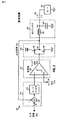
[0016] 図1は、オープン・ループ構造を有するスイッチング増幅器100の例示的な設計の概略図を示す。電力増幅器100は、変調器120および出力回路130を含む。図1に示されている例示的な設計では、変調器120は、入力信号S(t)を受信する反転入力、およびキャリア信号C(t)を受信する非反転入力を有するコンパレータ122によって実施される。コンパレータ122は、キャリア信号に対して入力信号を比較し、その比較の結果に基づいてドライブ信号D(t)を生成する。
[0016] FIG. 1 shows a schematic diagram of an exemplary design of a
[0017] キャリア信号は、スイッチング周波数とも称される固定の周波数を有する。キャリア信号は、(図1に示されているような)のこぎり形波形、三角形波形、四角形波形などを有し得る。ドライブ信号は、(i)キャリア信号の周波数によって決定される固定のスイッチング周波数、および(ii)入力信号の振幅によって決定される可変のデューティ・サイクルを有し得る。ドライブ信号は、本来デジタル式であり、ロジック・ハイ(例えば、電源電圧、Vdd)と、ロジック・ロー(例えば、回路グラウンド(circuit ground))とを切り替える。 [0017] The carrier signal has a fixed frequency, which is also referred to as a switching frequency. The carrier signal may have a sawtooth waveform (as shown in FIG. 1), a triangular waveform, a square waveform, and the like. The drive signal may have (i) a fixed switching frequency determined by the frequency of the carrier signal, and (ii) a variable duty cycle determined by the amplitude of the input signal. The drive signal is digital in nature and switches between logic high (eg, power supply voltage, Vdd) and logic low (eg, circuit ground).
[0018] 図1に示されている例示的な設計では、出力回路130は、Vdd電源および回路グラウンド間で、かつ直列に結合された2つのスイッチ132および134によって実施される。スイッチ132は、ノードN1に結合された1つの端末と、Vdd電源に結合された他の端末と、ドライブ信号を受信する制御インプットを有する。スイッチ134は、ノードN1に結合された1つの端末と、回路グラウンドに結合された他の端末と、ドライブ信号を受信する制御インプットを有する。スイッチ132は、Pチャンネル金属酸化膜半導体(PMOS)トランジスタ、および/または、いくつかの他の種類のトランジスタによって実施され得る。スイッチ134は、Nチャンネル金属酸化膜半導体(NMOS)トランジスタ、および/または、いくつかの他の種類のトランジスタによって実施され得る。出力回路130は、ノードN1において出力信号Y(t)を提供する。
[0018] In the exemplary design shown in FIG. 1,
[0019] 図1に示されている例示的な設計では、出力フィルタ140は、スイッチング増幅器100に結合されており、ローパス・フィルタを形成するコンデンサ144およびインダクタ142によって実施される。インダクタ142は、出力回路130から出力信号を受信する一方の端部、およびノードN2に結合された他方の端部を有する。コンデンサ144は、ノードN2および回路グラウンド間に結合されている。概して、出力フィルタ140は、任意の数の回路コンポーネントによって実施され得、ローパス・フィルタ、バンドパス・フィルタ、ハイパス・フィルタなどを備え得る。直流(DC)ブロッキング・コンデンサ146が、ノードN2およびロード150間に結合されている。
[0019] In the exemplary design shown in FIG. 1,
[0020] スイッチング増幅器100は、以下のように動作する。コンパレータ122が、キャリア信号のサイクルまたは周期の各々において、ドライブ信号でパルスを生成する。パルスの幅は、入力信号の振幅によって決定される。ドライブ信号は、キャリア周波数においてパルスのストリームを含み、PWM信号とも称され得る。入力信号がキャリア信号よりも高いとき、ドライブ信号はロジック・ローであり、スイッチ132が入れられ、スイッチ134が切られ、Vdd電圧が出力回路130からの出力信号に提供される。逆に、入力信号がキャリア信号よりも低いとき、ドライブ信号はロジック・ハイであり、スイッチ134が入れられ、スイッチ132が切られ、回路グラウンドに対応する低電圧が、出力回路130からの出力信号に提供される。出力回路130は、ドライブ信号に基づいて電流を供給する(source)か、吸収する(sink)。
The switching
[0021] 出力回路130からの出力信号は、本来デジタル式であり、キャリア信号の望ましくない高調波および所望の入力信号を含む。キャリア信号高調波は、キャリア/スイッチング周波数の整数倍である。出力フィルタ140は、出力信号をフィルタして、所望の入力信号を通し、望ましくないキャリア信号高調波および他の外部からの高周波数コンポーネントを減衰する。スイッチング周波数は、所望の入力信号の帯域幅よりはるかに高いこともあり得る。この場合、出力フィルタ140は、簡潔な下位のフィルタ(simple low-order filter)、例えば、コンデンサ144およびインダクタ142から成る2次LCフィルタによって実施され得る。
[0021] The output signal from
[0022] 図2は、クローズ・ループ構造を有するスイッチング増幅器102の例示的な設計の概略図を示す。電力増幅器102は、図1のパワー増幅器100内に変調器120および出力回路130を含む。電力増幅器102は、さらに、フィードバック回路110を含む。
[0022] FIG. 2 shows a schematic diagram of an exemplary design of switching
[0023] 図2に示されている例示的な設計では、フィードバック回路110は、サマー112およびループ・フィルタ114を含む。サマー112は、出力回路130から出力信号Y(t)および入力信号S(t)を受信し、入力信号から出力信号を差し引き、エラー信号を提供する。サマー112は、出力信号を受信する反転入力および入力信号を受信する非反転入力を有する増幅器によって実施され得る。ループ・フィルタ114は、エラー信号をフィルタし、変調器120内のコンパレータ122の反転入力に、フィルタされたエラー信号を提供する。スイッチング増幅器102におけるフィードバックの使用は、出力信号の電力電圧変動除去比(PSRR:power supply rejection ratio)および全高調波歪(THD:total harmonic distortion)を改良し得る。
In the exemplary design shown in FIG. 2,
[0024] 図1のスイッチング増幅器100および図2のスイッチング増幅器102は、クラスDの増幅器の2つの例示的な設計である。クラスDの増幅器が他のクラスの増幅器より優れた性能を有することは周知である。
[0024]
[0025] 図3Aは、異なるクラスの増幅器に関わる出力電力対効率のプロットを示す。図3Aにおいて、水平軸は、出力電力を示しており、ワット(W)の単位で与えられている。垂直軸は、効率を示しており、パーセント(%)の単位で与えられている。プロット310は、クラスABの増幅器に関わる出力電力対効率を示す。プロット312は、クラスDの増幅器に関わる出力電力対効率を示す。図3Aは、クラスDの増幅器がクラスABの増幅器よりはるかに高い効率を有することを示す。図3Aは、また、クラスDの増幅器が広範囲の出力電力レベルにわたって高い効率を得ることができることを示す。 [0025] FIG. 3A shows a plot of output power versus efficiency for different classes of amplifiers. In FIG. 3A, the horizontal axis indicates the output power and is given in units of watts (W). The vertical axis represents efficiency and is given in units of percent (%). Plot 310 shows the output power versus efficiency for a class AB amplifier. Plot 312 shows the output power versus efficiency for a class D amplifier. FIG. 3A shows that a class D amplifier has a much higher efficiency than a class AB amplifier. FIG. 3A also shows that class D amplifiers can obtain high efficiency over a wide range of output power levels.
[0026] 図3Bは、異なるクラスの増幅器に関わる出力電力対ワット損のプロットを示す。図3Bでは、水平軸は、出力電力を示しており、ワットの単位で与えられている。垂直軸は、増幅器によるワット損を示しており、ワットの単位で与えられている。プロット320は、クラスABの増幅器に関わる出力電力対ワット損を示す。プロット322は、クラスDの増幅器に関わる出力電力対ワット損を示す。図3Bは、クラスABの増幅器よりはるかに低いワット損を有することを示す。図3Bは、また、クラスDの増幅器のワット損が広範囲の出力電力レベルにわたって穏やかに上昇していることを示す。 [0026] FIG. 3B shows a plot of output power versus power dissipation for different classes of amplifiers. In FIG. 3B, the horizontal axis shows the output power and is given in units of watts. The vertical axis shows the power dissipation due to the amplifier and is given in units of watts. Plot 320 shows output power versus power dissipation for a class AB amplifier. Plot 322 shows output power versus power dissipation for a class D amplifier. FIG. 3B shows that it has a much lower power dissipation than a class AB amplifier. FIG. 3B also shows that the power dissipation of Class D amplifiers rises gently over a wide range of output power levels.
[0027] 図3Aおよび図3Bに示されているように、クラスDの増幅器を実施するスイッチング増幅器は、他のクラスの増幅器より優れた性能を有し得る。しかしながら、スイッチング増幅器からの出力信号は、望ましくないキャリア信号コンポーネントおよび所望の入力信号コンポーネントを含む。図1および図2に示されているように、出力フィルタ140は、望ましくないキャリア信号高調波を減衰するために使用され得る。出力フィルタ140は、キャリア信号高調波の所望量のフィルタリングを提供するために、大きな回路コンポーネント(例えば、1つ以上のインダクタ、および/または1つ以上の大きなコンデンサ)を含み得る。例えば、入力信号は、100メガヘルツ(MHz)の帯域幅を有し得、キャリア信号は、1ギガヘルツ(GHz)の固定の周波数を有し得る。1GHzでキャリア信号の50デシベル(dB)の減衰を得るために、出力フィルタ140は、100ナノヘンリー(nH)の値を有するインダクタ142と、80ピコファラッド(pF)の値を有するコンデンサ144によって実施され得る。そして、出力フィルタ140は、比較的大きいインダクタと比較的大きいコンデンサのために、大きい回路面積を占有するだろう。さらに、出力フィルタ140は、56MHzの比較的狭い帯域幅を有し、それは、入力信号の100MHzの帯域幅より小さい。したがって、入力信号のより高い周波数コンポーネントは、出力フィルタ140のこの比較的狭い帯域幅によって減衰されるだろう。
[0027] As shown in FIGS. 3A and 3B, a switching amplifier implementing a class D amplifier may have better performance than other classes of amplifiers. However, the output signal from the switching amplifier includes an undesirable carrier signal component and a desired input signal component. As shown in FIGS. 1 and 2,
[0028] 本開示の態様では、スイッチング増幅器は、キャリア信号の高調波を減衰することができる組み込まれた高調波除去フィルタを含む。高調波除去は、複数の異なる遅延を伴う複数のドライブ信号を生成すること、複数の出力回路にドライブ信号を適用すること、および出力回路の出力を合わせ、合わせられた信号を得ること、によって、達成される。このような合わせられた信号は、高調波周波数においてゼロを有する伝達関数によって乗じられた1つのドライブ信号のスペクトルと等しいスペクトルを有する。キャリア信号高調波は伝達関数によって減衰されるので、スイッチング増幅器に結合された出力フィルタの要件が緩和され得る。かくして、出力フィルタは、緩和された要件のために、より小さい回路コンポーネントによって実施され得、かつより小さい回路面積を占有し得る。 [0028] In aspects of the disclosure, the switching amplifier includes an integrated harmonic rejection filter that can attenuate harmonics of the carrier signal. Harmonic rejection involves generating multiple drive signals with multiple different delays, applying the drive signal to multiple output circuits, and combining the outputs of the output circuits to obtain a combined signal, Achieved. Such a combined signal has a spectrum equal to the spectrum of one drive signal multiplied by a transfer function having zero at the harmonic frequency. Since the carrier signal harmonics are attenuated by the transfer function, the requirements of the output filter coupled to the switching amplifier can be relaxed. Thus, the output filter may be implemented with smaller circuit components and occupy less circuit area due to relaxed requirements.
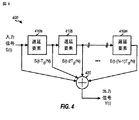
[0029] 図4は、組み込まれた高調波除去フィルタのために使用され得るFIRフィルタ400の例示的な設計を示す。FIRフィルタ400は、直列に結合されたN−1の遅延要素410a乃至410mを含み、ここにおいて、Nは、1より大きい任意の整数値であり得る。各遅延要素410は、T0/Nの遅延を提供し、ここにおいて、T0は、キャリア信号の1周期である。
[0029] FIG. 4 shows an exemplary design of a
[0030] 入力信号S(t)は、FIRフィルタ400における第1の遅延要素410aに提供される。各遅延要素410は、異なる遅延を有するそれぞれの遅延した入力信号を提供する。N−1の遅延要素410a乃至410mからのN−1の遅延した入力信号、および1つの入力信号は、異なる量の遅延に関連したNの遅延信号のセットを形成する。Nの遅延信号のこのセットは、S(t)、S(t−T0/N)、S(t−2T0/N)、・・・、S(t−(N−1)・T0/N)と示され、サマー420によって合わせられて出力信号Y(t)を生成し、それは以下のように表され得る。

ここにおいて、bnは、n次のFIRフィルタ・タップの係数(coefficient for the n-th FIR filter tap)である。係数bnは、図4のFIRフィルタ400に対して1と等しいが、所望のフィルタ応答を得るために他の値と等しいこともあり得る。
Here, b n is a coefficient for the n-th FIR filter tap. The coefficient b n is equal to 1 for the
[0031] 周波数領域における出力信号は、以下のように表され得る。
ここにおいて、S(ω)は、周波数領域における入力信号を示し、Y(ω)は、周波数領域における出力信号を示し、H(ω)は、FIRフィルタ400の伝達関数を示す。ここにおいて、ω=2π・fであり、ここでfは周波数を示し、および、ω0=2π・f0であり、ここでf0はキャリア信号の周波数を示す。
Here, S (ω) represents an input signal in the frequency domain, Y (ω) represents an output signal in the frequency domain, and H (ω) represents a transfer function of the
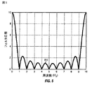
[0032] 図5は、図4のFIRフィルタ400の伝達関数H(ω)のプロット510を示す。水平軸は、周波数を示しており、f/f0の単位で与えられている。垂直軸は、振幅を示しており、線形ユニットで与えられている。図5は、N=10による一例を示す。図5に示されているように、FIRフィルタ400の伝達関数H(ω)は、ω=k・ω0に関してゼロの値を有し、ここにおいてk=1、2…、N−1である。これは、出力信号Y(k・ω0)がキャリア周波数ω0の全ての高調波においてゼロと等しいことを意味する。
FIG. 5 shows a
[0033] スイッチング増幅器は、キャリア信号の高調波を減衰するために、組み込まれたFIRフィルタを含み得、ω0において基本波(fundamental harmonic)を含む。FIRフィルタは、また、折返し雑音(noise folding)を減じ、このことが、性能を向上し得る。スイッチング増幅器は、様々なやり方で実施され得、いくつかの例示的な設計が以下に説明される。 [0033] The switching amplifier may include an embedded FIR filter to attenuate the harmonics of the carrier signal, including a fundamental harmonic at ω 0 . FIR filters also reduce noise folding, which can improve performance. Switching amplifiers can be implemented in various ways, and some exemplary designs are described below.
[0034] 図6Aは、組み込まれた高調波除去フィルタを有するスイッチング増幅器600の例示的な設計の概略図を示す。スイッチング増幅器600は、異なる量だけキャリア信号を遅延させることによって、高調波除去のためのFIRフィルタを実施する。スイッチング増幅器600は、ジェネレータ回路601、およびNの出力回路630a乃至630nを含む。ジェネレータ回路601は、Nのコンパレータ(Comp)622a乃至622nを備えるNの変調器620、およびN−1の遅延回路610b乃至610nを含む。キャリア信号C(t)は、N−1の遅延回路610b乃至610nの各々に提供され、それらは、T0/N乃至(N−1)・T0/Nの異なる遅延をそれぞれ提供する。N次の遅延回路610は、n次の遅延キャリア信号Cn(t)=C(t−n・T0/N)を提供し、ここで、n=1、2、・・・、N−1である。
[0034] FIG. 6A shows a schematic diagram of an exemplary design of a switching
[0035] コンパレータ622aは、一方の入力においてキャリア信号を、他方の入力において入力信号S(t)を受信し、第1のドライブ信号D0(t)を提供する。コンパレータ622bは、一方の入力において遅延回路610bから遅延キャリア信号を、他方の入力において入力信号を受信し、第2のドライブ信号D1(t)を提供するのであり、それは、遅延バージョンの第1のドライブ信号、または、D1(t)=D0(t−T0/N)である。残りのコンパレータ622の各々は、一方の入力において対応する遅延回路610から遅延キャリア信号を、他方の入力において入力信号を受信し、対応するドライブ信号を提供する。n次のコンパレータ622は、n次のドライブ信号Dn(t)=D0(t−n・T0/N)を提供し、ここで、n=0、1、2、・・・、N−1である。
The
[0036] 出力回路630a乃至630nは、コンパレータ622a乃至622nからそれぞれドライブ信号を受信する。各出力回路630iは、ここではi=a、b、・・・、nであり、その出力をVdd電源または回路グラウンドの何れかに結合するように、それぞれのドライブ信号によって制御される。各出力回路630iは、PMOSトランジスタ632およびNMOSトランジスタ634によって実施され得る。PMOSトランジスタ632は、Vdd電源に結合されたソースと、出力回路630iの出力に結合されたドレインを有する。NMOSトランジスタ634は、回路グラウンドに結合されたソースと、出力回路630iの出力に結合されたドレインを有する。PMOSトランジスタ632のゲートのための制御信号およびNMOSトランジスタ634は、出力回路630iのためのドライブ信号に基づいて生成され得る。全てのNの出力回路630a乃至630nの出力は、ノードUにおいて一緒に結合され、合わせられる。
The
[0037] 1つの例示的な設計では、各出力回路630は、図6Aに示されているように、プッシュプル・トランジスタ(push-pull transistor)によって実施され得る。他の例示的な設計では、出力回路は、デジタル/アナログ変換機(DAC)によって実施され得る。出力回路は、また、他の回路によって実施され得る。 [0037] In one exemplary design, each output circuit 630 may be implemented with a push-pull transistor, as shown in FIG. 6A. In other exemplary designs, the output circuit may be implemented by a digital / analog converter (DAC). The output circuit can also be implemented by other circuits.
[0038] ノードUにおける出力信号Y(t)は、数式(1)に示されているように表され得る。概して、Nの出力回路630a乃至630nは、同じ利得、または異なる利得を有し得る。図5に示されている周波数応答は、数式(1)において、bn=1、ここではn=0、1、2、・・・、N−1、または、Nの出力回路630a乃至630nに対して同じ利得で得られ得る。所望の周波数応答(例えば、ローパス・フィルタ、バンドパス・フィルタ、またはハイパス・フィルタ)は、Nの出力回路630a乃至630nに対して不均一な利得で得られ得る。異なる出力回路に対する異なる利得は、様々なやり方で得られ得る。1つの例示的な設計では、より高い利得が、並列で結合されたより多くのPMOSトランジスタ、および/または、より多くのNMOSトランジスタを使用することによって、所定の出力回路630に対して得られ得、より多くのカレント・ドライブを提供する。他の例示的な設計では、より高い利得が、より大きなNMOSトランジスタ、および/または、より大きなPMOSトランジスタを使用することによって、所定の出力回路630に対して得られ得る。さらなる他の例示的な設計では、より高い利得が、より高い電源電圧を使用することによって、所定の出力回路630に対して得られ得る。
[0038] The output signal Y (t) at the node U may be expressed as shown in Equation (1). In general, the
[0039] 図6Aに示されている例示的な設計では、出力フィルタ640は、スイッチング増幅器600に結合されており、ローパス・フィルタを形成するコンデンサ644およびインダクタ642によって実施される。インダクタ642およびコンデンサ644は、図1の出力フィルタ140内のコンデンサ144およびインダクタ142と同様のやり方で結合されている。出力フィルタ640は、スイッチング増幅器600の組み込まれた高調波除去フィルタによるキャリア信号高調波の減衰の結果としての緩和されたフィルタリング要件のために、より小さなコンデンサ、および/または、より小さなインダクタによって実施され得る。100MHzの入力信号帯域幅および1GHzのキャリア周波数によって上記で説明した例では、出力フィルタ640は、5bHの値を有するインダクタ642および1pFの値を有するコンデンサ644によって、50dBのキャリア信号高調波の除去を提供することができる。逆に、組み込まれた高調波除去フィルタがない場合、図1の出力フィルタ140は、さらにより大きい値80pFを有するコンデンサ144およびさらにより大きい値100nHを有するインダクタ142によって、50dBのキャリア信号高調波の除去を提供することができる。かくして、出力フィルタ640は、出力フィルタ140よりさらにより小さい回路面積を占有し得る。
[0039] In the exemplary design shown in FIG. 6A,
[0040] スイッチング増幅器600は、図6Aに示されているように、オープン・ループのやり方で動作され得る。スイッチング増幅器600は、また、例えば図2に示されているようなループ・フィルタおよびサマーを有するフィードバック回路を含むことによって、クローズ・ループのやり方で動作され得る。この場合では、入力信号および出力信号は、サマーに提供され得、それは、ループ・フィルタにエラー信号を提供し得る。(入力信号ではなく)フィルタされたエラー信号は、Nのコンパレータ622a乃至622nに、ループ・フィルタによって提供され得る。
[0040]
[0041] 図6Aのスイッチング増幅器600は、いくつかの新規な特徴を有する。第1に、出力回路630および変調器620の複数のステージが、並行に結合され、全ての出力回路630の出力は、加算ノード(summing node)Uにおいて一緒に結合される。第2に、Nの変調器620に提供されたキャリア信号は、徐々に遅延される。第3に、信号出力フィルタ640は、全てのNの出力回路630a乃至630nの加算された出力のために使用される。
[0041] The switching
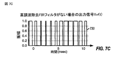
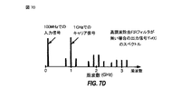
[0042] 図7A乃至図7Eは、図6Aにおいてスイッチング増幅器に関連したさまざまな信号を示す。図7Aは、スイッチング増幅器600に提供された入力信号S(t)のプロット710を示す。この例では、入力信号は、100MHzの周波数において、正弦関数を備える。図7Bは、スイッチング増幅器600に提供されたキャリア信号C(t)のプロット720を示す。この例では、キャリア信号は、1GHzの周波数において、のこぎり形信号である。図7Cは、組み込まれた高調波除去フィルタがない場合のスイッチング増幅器の出力回路によって与えられる出力信号Ynf(t)のプロット730を示す。この出力信号Ynf(t)は、図6Aの出力回路630aからの出力信号Y0(t)と等しく、残りのN−1の出力回路630b乃至630nに接続されないことが、想定される。出力信号Ynf(t)は、入力信号の振幅に依存するデューティ・サイクルおよび1GHzの周波数を有する。
[0042] FIGS. 7A-7E illustrate various signals associated with the switching amplifier in FIG. 6A. FIG. 7A shows a
[0043] 図7Dは、図7Cの出力信号Ynf(t)の周波数応答のプロットを示す。図7Dに示されているように、出力信号Ynf(t)は、100MHzでの所望の入力信号、および、1GHzでの望ましくないキャリア信号、および他の望ましくない信号コンポーネントを含む。図7Eは、図6AのNの出力回路630a乃至630nの組み合された出力からの、組み込まれた高調波除去フィルタによる、出力信号Y(t)の周波数応答のプロットを示す。図7Eに示されているように、出力信号Y(t)は、100MHzの所望の入力信号を含み、望ましくないキャリア信号高調波を、含まないか最小限にのみ含む。図7Dおよび図7Eは、望ましくないキャリア信号高調波を減衰する際の、組み込まれた高調波除去フィルタの有効性を示す。図7Eは、キャリア信号の全ての高調波を減衰する組み込まれた高調波除去フィルタを示し、それは、1GHzでの基本波を含む。ここに開示される高調波除去技術は、ω0における信号コンポーネントを保存するように試みながらも残りの高調波ω=k・ω0、ここではk≧2、をフィルタして除去するように試みる、高調波除去ミキサ技術(harmonic rejection mixer technique)とは異なる。
[0043] FIG. 7D shows a plot of the frequency response of the output signal Y nf (t) of FIG. 7C. As shown in FIG. 7D, the output signal Y nf (t) includes a desired input signal at 100 MHz, an undesirable carrier signal at 1 GHz, and other undesirable signal components. FIG. 7E shows a plot of the frequency response of the output signal Y (t) with the integrated harmonic rejection filter from the combined output of the
[0044] 図6Bは、組み込まれた高調波除去フィルタを有するスイッチング増幅器602の例示的な設計の概略図を示す。スイッチング増幅器602は、異なる量だけ入力信号を遅延させることによって高調波除去のためのFIRフィルタを実施する。スイッチング増幅器602は、ジェネレータ回路603およびNの出力回路630a乃至630nを含む。ジェネレータ回路603は、Nのコンパレータ622a乃至622nを備えるNの変調器620およびN−1の遅延回路610b乃至610nを含む。入力信号S(t)は、T0/N乃至(N−1)・T0/Nの異なる遅延をそれぞれ提供するN−1の遅延回路610b乃至610nの各々に提供される。N次の遅延回路610は、n次の遅延入力信号を提供する。Nのコンパレータ622a乃至622nは、それぞれ異なる量の遅延に関連したNの入力信号S0(t)乃至SN−1(t)、および同じキャリア信号C(t)を受信する。各コンパレータ622は、遅延した入力信号およびキャリア信号に基づいたそれぞれのドライブ信号を生成する。Nのコンパレータ622a乃至622nは、Nのドライブ信号D0(t)乃至DN−1(t)をそれぞれ提供する。
[0044] FIG. 6B shows a schematic diagram of an exemplary design of a switching
[0045] 図6Cは、組み込まれた高調波除去フィルタを有するスイッチング増幅器604の例示的な設計の概略図を示す。スイッチング増幅器604は、異なる量だけドライブ信号を遅延することによって高調波除去のためのFIRフィルタを実施する。スイッチング増幅器604は、ジェネレータ回路605およびNの出力回路630a乃至630nを含む。ジェネレータ回路605は、N−1の遅延回路610b乃至610n、および、コンパレータ622xを備える1つの変調器620xを含む。コンパレータ622xは、入力信号S(t)およびキャリア信号C(t)を受信し、ドライブ信号D(t)を提供する。ドライブ信号は、出力回路630aに、および、N−1の遅延回路610b乃至610nの各々にも、提供される。遅延回路610b乃至610nは、T0/N乃至(N−1)・T0/Nの異なる遅延をそれぞれ提供する。n次の遅延回路610は、n次の遅延したドライブ信号を提供する。各出力回路630は、それぞれのドライブ信号を受信し、そのドライブ信号によって制御される。
[0045] FIG. 6C shows a schematic diagram of an exemplary design of switching
[0046] 図6Bのスイッチング増幅器602および図6Cのスイッチング増幅器604は、図6Aのスイッチング増幅器600と機能的に同等である。異なる量の遅延に関連したNのドライブ信号D0(t)乃至DN−1(t)は、(例えば図6Aに示されているような)キャリア信号を遅延すること、または、(例えば図6Bに示されているような)入力信号を遅延すること、または、(例えば図6Cに示されているような)ドライブ信号を遅延することによって、得られ得る。
[0046]
[0047] 図6A乃至図6Cは、組み込まれた高調波除去フィルタを有するスイッチング増幅器の3つの例示的な設計を示す。他の例示的な設計では、組み込まれた高調波除去フィルタを有するスイッチング増幅器は、図6Cのコンパレータ622xとは代わって、位相ロック・ループ(PLL:phase locked loop)を備えるジェネレータ回路を含み得る。PLLは、入力信号S(t)および基準クロック(reference clock)を受信し、ドライブ信号D(t)を提供し得る。PLLは、ダイレクトFM(direct FM)を実施し得る。組み込まれた高調波除去フィルタを有するスイッチング増幅器は、他のやり方でも実施され得る。
[0047] FIGS. 6A-6C illustrate three exemplary designs of a switching amplifier with an integrated harmonic rejection filter. In another exemplary design, a switching amplifier with an integrated harmonic rejection filter may include a generator circuit with a phase locked loop (PLL) instead of the
[0048] 組み込まれた高調波除去フィルタを有するスイッチング増幅器は、例えば図6A乃至図6Cに示されているような、シングルエンドの設計(single-ended design)によって実施され得る。組み込まれた高調波除去フィルタを有するスイッチング増幅器は、異なる設計によっても実施され得る。例えば、図6Aの回路が反復され得る。非反転入力信号S(t)および非反転キャリアC(t)は、非反転出力信号Y(t)を生成するために回路の第1のコピーに提供され得る。反転入力信号
および反転キャリア
は、反転出力信号
を生成するために、回路の第2のコピーに提供され得る。反転および非反転出力信号は、1つ以上の出力信号に提供され得る。 Can be provided to a second copy of the circuit. Inverted and non-inverted output signals may be provided to one or more output signals.
[0049] 例示的な設計では、複数のスイッチング増幅器は、各々が組み込まれた高調波除去フィルタを有しており、望ましくない帯域外信号コンポーネントの減衰を改良するために、カスケード/直列で結合され得る。概して、組み込まれた高調波除去フィルタを有する任意の数のスイッチング増幅器は、カスケードで結合され得る。スイッチング増幅器は、同一であり得、また、異なる設計を有し得る。 [0049] In an exemplary design, a plurality of switching amplifiers each have a built-in harmonic rejection filter and are coupled in cascade / series to improve attenuation of unwanted out-of-band signal components. obtain. In general, any number of switching amplifiers with integrated harmonic rejection filters can be coupled in cascade. The switching amplifiers can be the same and can have different designs.
[0050] 図8は、カスケードで結合された2つのスイッチング増幅器800aおよび800bの例示的な設計のブロック図を示し、各スイッチング増幅器800は、組み込まれた高調波除去フィルタを有する。スイッチング増幅器800aは、入力信号S(t)およびキャリア信号C(t)を受信し、中間信号X(t)を提供する。スイッチング増幅器800bは、中間信号X(t)およびキャリア信号C(t)を受信し、出力信号Y(t)を提供する。出力フィルタ(図8には示されていない)は、出力信号Y(t)を受信し、フィルタし得る。
[0050] FIG. 8 shows a block diagram of an exemplary design of two switching amplifiers 800a and 800b coupled in cascade, each switching
[0051] スイッチング増幅器800aおよび800bは、図6Aのスイッチング増幅器600、図6Bのスイッチング増幅器602、図6Cのスイッチング増幅器604、またはいくつかの他の設計のスイッチング増幅器によって各々実施され得る。スイッチング増幅器800aおよび800bは、同じ数のステージ/タップまたは異なる数のステージを有し得る。スイッチング増幅器800aおよび800bは、(例えば、図8に示されているような)同じキャリア信号を受信し得、または、異なるキャリア信号を受信し得る。例えば、スイッチング増幅器800aは、第1の周波数で第1のキャリア信号を受信し得、スイッチング増幅器800bは、第2の周波数で第2のキャリア信号を受信し得る。第1および第2の周波数は、整数比によって関連し得る。
[0051] Switching amplifiers 800a and 800b may each be implemented by switching
[0052] 図9は、図8のスイッチング増幅器800aおよび800bの周波数応答のプロットを示す。水平軸は、周波数を示しており、f/f0の単位で与えられている。垂直軸は、振幅を示しており、線形ユニットで与えられている。プロット910は、N=6の場合における単一のスイッチング増幅器800aまたは800bの周波数応答を示す。プロット920は、N=6の場合におけるスイッチング増幅器800aおよび800bの両方の全体の周波数応答を示す。図9に示されているように、カスケードの複数のスイッチング増幅器(cascading multiple switching amplifiers)は、f0、2f0、3f0などでキャリア信号の高調波をさらに減衰し得る。 [0052] FIG. 9 shows a plot of the frequency response of the switching amplifiers 800a and 800b of FIG. The horizontal axis shows the frequency, it is given in units of f / f 0. The vertical axis shows the amplitude and is given in linear units. Plot 910 shows the frequency response of a single switching amplifier 800a or 800b when N = 6. Plot 920 shows the overall frequency response of both switching amplifiers 800a and 800b for N = 6. As shown in FIG. 9, cascading multiple switching amplifiers can further attenuate the harmonics of the carrier signal at f 0 , 2f 0 , 3f 0 , and so on.
[0053] 複数の遅延回路610b乃至610nは、異なる量の遅延を提供するために使用され得、さまざまなやり方で実施され得る。遅延回路は、アナログ回路、またはデジタル回路、または、これら両方の組み合わせによって実施され得る。 [0053] The plurality of delay circuits 610b-610n may be used to provide different amounts of delay and may be implemented in various ways. The delay circuit may be implemented by an analog circuit, a digital circuit, or a combination of both.
[0054] 図10は、遅延回路ブロック1000の例示的な設計の概略図を示しており、それは、図6A乃至6Cの遅延回路610b乃至610nを実施するために使用され得る。図10に示されている例示的な設計では、遅延回路ブロック1000は、カスケード/直列で結合されたN−1のバッファ(Buf)1010b乃至1010nを含む。各バッファ1010は、T0/Nの遅延を提供する。入ってくる信号Q(t)は、第1のバッファ1010bの入力に提供される。各バッファは、次のバッファの入力に、それぞれ遅延した信号を提供する。N−1のバッファ1010b乃至1010nは、N−1の遅延した信号Q1(t)乃至QN−1(t)を提供し、ここで、Q0(t)=Q(t)およびQi(t)=Qi−1(t−T0/N)であり、ここでi=1、2、・・・、N−1である。
[0054] FIG. 10 shows a schematic diagram of an exemplary design of
[0055] 1つの例示的な設計では、バッファ1010b乃至1010nは、固定の遅延を各々提供し得る。他の例示的な設計では、バッファ1010b乃至1010nは、設定可能な遅延を各々提供し得る。例えば、各バッファ1010は、並行して結合された複数のMOSトランジスタによって実施され得る。より多くのMOSトランジスタが、より短い遅延を得るために作動され、逆の場合もまた同様である。他の例として、各バッファ1010は、コンデンサのバンクを含み得る。より少ないコンデンサが、より短い遅延を得るために選択され得、逆の場合もまた同様である。何れの場合も、N−1のバッファは、所望の量の遅延を提供するために設定され得る。N−1のバッファ1010b乃至1010nは、それらが全てのバッファに対して適した遅延を得るために可能な限り近接して一緒に一致するように、(例えば、オンチップで(on chip))実施され得る。
[0055] In one exemplary design, the buffers 1010b-1010n may each provide a fixed delay. In another exemplary design, buffers 1010b-1010n may each provide a configurable delay. For example, each
[0056] 他の例示的な設計では、複数の異なる遅延を有する複数の異なるバージョンの所定の信号が、これら異なるバージョンの信号をデジタル的に合成することによって、得られ得る。例えば、異なるバージョンの信号は、当業者には周知の直接デジタル合成(DDS:direct digital synthesis)に基づくルックアップ・テーブルから合成され得る。 [0056] In another exemplary design, a plurality of different versions of a predetermined signal having a plurality of different delays may be obtained by digitally combining the different versions of the signal. For example, different versions of the signal may be synthesized from a look-up table based on direct digital synthesis (DDS) well known to those skilled in the art.
[0057] 1つの例示的な設計では、組み込まれた高調波除去フィルタを有するスイッチング増幅器の出力回路およびコンパレータは、適切な回路コンポーネント(例えば、MOSトランジスタ)によって実施され得る。他の例示的な設計では、複数の出力回路に対する複数のドライブ信号が、(キャリア信号を使用するコンパレータによってではなく)デジタル領域で生成され得る。この例示的な設計では、FIRフィルタは、1ビット幅のインプット信号を受信するデジタル回路に形成され、Nビット幅のサーモメータ符号化出力信号(thermometer-coded output signal)を生成し得る。そして、スイッチング増幅器は、出力フィルタを駆動するDACおよびデジタル回路によって実施され得る。 [0057] In one exemplary design, the output circuit and comparator of a switching amplifier with an integrated harmonic rejection filter may be implemented with appropriate circuit components (eg, MOS transistors). In another exemplary design, multiple drive signals for multiple output circuits may be generated in the digital domain (not by a comparator using a carrier signal). In this exemplary design, the FIR filter may be formed in a digital circuit that receives a 1-bit wide input signal to generate an N-bit wide thermometer-coded output signal. The switching amplifier can then be implemented by a DAC and digital circuit that drives the output filter.
[0058] 組み込まれた高調波除去フィルタを有するスイッチング増幅器は、組み込まれた高調波除去フィルタのない増幅器に勝る様々な有利な点を提供し得る。スイッチング増幅器は、望ましくない信号コンポーネントのフィルタリングを実施するための時間遅延を伴う、並列で結合された出力回路の複数のステージを含む。結果として、はるかに小さいサイズの出力フィルタ(例えば、より小さいインダクタ、および/または、より小さいコンデンサ)は、出力回路の後に所望の信号コンポーネントの所望の減衰を提供することができる。より小さい出力フィルタは、出力回路によって、オンチップで実施され得る。出力回路および出力フィルタの完全な統合は、複雑さおよびコストを減じ、性能を向上させ、および/または他の利益を提供し得る。 [0058] Switching amplifiers with an integrated harmonic rejection filter may provide various advantages over amplifiers without an integrated harmonic rejection filter. The switching amplifier includes multiple stages of output circuits coupled in parallel with a time delay to perform filtering of undesirable signal components. As a result, a much smaller sized output filter (eg, a smaller inductor and / or a smaller capacitor) can provide the desired attenuation of the desired signal component after the output circuit. The smaller output filter can be implemented on-chip by the output circuit. Full integration of the output circuit and output filter may reduce complexity and cost, improve performance, and / or provide other benefits.
[0059] 例示的な設計では、装置(例えば、無線デバイス、集積回路(IC)、回路モジュールなど)は、ジェネレータ回路、および複数の出力回路を含み得、組み込まれた高調波除去フィルタを有するスイッチング増幅器を実施し得る。ジェネレータ回路は、入力信号およびキャリア信号を受信し得、複数の異なる遅延に関連した複数のバージョンの1つのドライブ信号を生成し得る。複数の出力回路は、複数のバージョンの1つのドライブ信号を受信し得、出力信号を提供し得る。複数の出力回路は、一緒に結合された出力を有し得、複数のバージョンの1つのドライブ信号に基づいてFIRフィルタを実施し得る。 [0059] In an exemplary design, an apparatus (eg, a wireless device, an integrated circuit (IC), a circuit module, etc.) may include a generator circuit, and a plurality of output circuits, switching with an integrated harmonic rejection filter. An amplifier may be implemented. The generator circuit may receive the input signal and the carrier signal and may generate multiple versions of one drive signal associated with multiple different delays. The plurality of output circuits may receive a plurality of versions of one drive signal and provide an output signal. Multiple output circuits may have outputs coupled together and may implement FIR filters based on multiple versions of one drive signal.
[0060] 複数のバージョンの1つのドライブ信号は、キャリア周波数でキャリア信号に基づいて生成され得る。FIRフィルタは、(例えば、図5および図9に示されているように)キャリア周波数の高調波で複数のゼロを伴う周波数応答を有し得る。キャリア信号は、(例えば、図7Bにおいて示されているような)三角形の波形、のこぎり型の波形、四角形の波形、または他の波形を有し得る。ドライブ信号は、PWM信号またはいくつかの他の変調された信号を備え得る。 [0060] One version of the drive signal may be generated based on the carrier signal at a carrier frequency. An FIR filter may have a frequency response with multiple zeros at harmonics of the carrier frequency (eg, as shown in FIGS. 5 and 9). The carrier signal may have a triangular waveform (eg, as shown in FIG. 7B), a sawtooth waveform, a square waveform, or other waveform. The drive signal may comprise a PWM signal or some other modulated signal.
[0061] 1つの例示的な設計では、1つのドライブ信号の複数のバージョンは、例えば図6Aに示されているように、キャリア信号を遅延させることによって発生され得る。この例示的な設計では、ジェネレータ回路は、少なくとも1つの遅延回路および複数の変調器を備え得る。少なくとも1つの遅延回路は、キャリア信号を受信し、複数の異なる遅延に関連したキャリア信号の複数のバージョンのうちの少なくとも1つを提供し得る。複数の変調器は、(全ての変調器に適用される)入力信号および1つのキャリア信号の複数のバージョンを受信し得、1つのドライブ信号の複数のバージョンを提供し得る。 [0061] In one exemplary design, multiple versions of a single drive signal, for example, as shown in Figure 6A, it may be generated by delaying the carrier signal. In this exemplary design, the generator circuit may comprise at least one delay circuit and a plurality of modulators. At least one delay circuit receives the carrier signal, can provide at least one more version sac Chino related carrier signals to a plurality of different delays. A plurality of modulators may provide a plurality of versions of the received obtain multiple versions of the input signals and one carrier signal (all applied to the modulator), one drive signal.
[0062] 他の例示的な設計では、複数のバージョンの1つのドライブ信号は、例えば図6Bに示されているように、入力信号を遅延させることによって生成され得る。この例示的な設計では、ジェネレータ回路は、少なくとも1つの遅延回路および複数の変調器を備え得る。少なくとも1つの遅延回路は、入力信号を受信し得、複数の異なる遅延に関連した複数のバージョンの入力信号のうちの少なくとも1つを提供し得る。複数の変調器は、複数のバージョンの入力信号および(全ての変調器に適用される)キャリア信号を受信し得、複数のバージョンの1つのドライブ信号を提供し得る。 [0062] In another exemplary design, multiple versions of a single drive signal may be generated by delaying the input signal, eg, as shown in FIG. 6B. In this exemplary design, the generator circuit may comprise at least one delay circuit and a plurality of modulators. At least one delay circuit may receive the input signal and may provide at least one of a plurality of versions of the input signal associated with a plurality of different delays. Multiple modulators may receive multiple versions of an input signal and a carrier signal (applied to all modulators) and may provide multiple versions of one drive signal.
[0063] さらなる他の例示的な設計では、複数のバージョンの1つのドライブ信号は、例えば図6Cに示されているように、ドライブ信号を遅延させることによって、生成され得る。この例示的な設計では、ジェネレータ回路は、少なくとも1つの遅延回路および1つの変調器を備え得る。変調器は、入力信号およびキャリア信号を受信し得、ドライブ信号を提供し得る。少なくとも1つの遅延回路は、ドライブ信号を受信し得、複数のバージョンのドライブ信号のうちの少なくとも1つを提供し得る。複数のバージョンの1つのドライブ信号は、他のやり方でも生成され得る。ジェネレータ回路は、1つまたは複数の適切な信号に基づいて複数のバージョンの1つのドライブ信号を生成することができるアナログ回路、および/または、デジタル回路を備え得る。 [0063] In yet another exemplary design, multiple versions of a single drive signal may be generated, for example, by delaying the drive signal, as shown in FIG. 6C. In this exemplary design, the generator circuit may comprise at least one delay circuit and one modulator. The modulator may receive an input signal and a carrier signal and provide a drive signal. The at least one delay circuit may receive the drive signal and provide at least one of the multiple versions of the drive signal. Multiple versions of a single drive signal may be generated in other ways. The generator circuit may comprise an analog circuit and / or a digital circuit capable of generating multiple versions of one drive signal based on one or more suitable signals.
[0064] 1つの例示的な設計では、各出力回路は、例えば図6A乃至図6Cに示されているように、第1および第2のトランジスタを含み得る。第1のトランジスタ(例えば、PMOSトランジスタ632)は電源電圧および出力回路の出力の間で結合され得る。第2のトランジスタ(例えば、NMOSトランジスタ634)は、回路グラウンドおよび出力回路の出力の間で結合され得る。1つの例示的な設計では、複数の出力回路は等しい利得を有し得、FIRフィルタは、図5に示されている周波数応答を有し得る。他の例示的な設計では、複数の出力回路は、少なくとも2つの異なる利得を有し得る。FIRフィルタは、各出力回路の利得に基づいて決定された適切な周波数応答を有し得る。 [0064] In one exemplary design, each output circuit may include first and second transistors, for example, as shown in FIGS. 6A-6C. A first transistor (eg, PMOS transistor 632) may be coupled between the power supply voltage and the output of the output circuit. A second transistor (eg, NMOS transistor 634) may be coupled between circuit ground and the output of the output circuit. In one exemplary design, the multiple output circuits may have equal gain and the FIR filter may have the frequency response shown in FIG. In other exemplary designs, the plurality of output circuits may have at least two different gains. The FIR filter may have an appropriate frequency response determined based on the gain of each output circuit.
[0065] 1つの例示的な設計では、出力フィルタは、複数の出力回路の組み合された出力に結合され得る。出力フィルタは、任意のフィルタのタイプ(例えば、ローパス、バンドパス、またはハイパス)であり得、任意の次数(order)を有し得る。1つの例示的な設計では、少なくとも1つの変調器、複数の出力回路、および出力フィルタは、同じICチップにおいて実施され得る。あるいは、少なくとも1つの変調器、および複数の出力回路は、ICチップにおいて実施され得、出力フィルタは、ICチップの外部で実施され得る。 [0065] In one exemplary design, the output filter may be coupled to the combined output of multiple output circuits. The output filter can be of any filter type (eg, low pass, band pass, or high pass) and can have any order. In one exemplary design, at least one modulator, multiple output circuits, and output filters may be implemented on the same IC chip. Alternatively, the at least one modulator and the plurality of output circuits can be implemented in an IC chip and the output filter can be implemented outside the IC chip.
[0066] 1つの例示的な設計では、複数の出力回路は、例えば図1に示されているように、オープン・ループ構造で使用される。この場合では、出力信号は、複数のバージョンの1つのドライブ信号を生成するために使用されない。他の例示的な設計では、複数の出力回路は、例えば図2に示されているように、クローズ・ループ構造で使用される。この場合では、出力信号は、フィードバックされ、複数のバージョンの1つのドライブ信号を生成するために使用され得る。 [0066] In one exemplary design, multiple output circuits are used in an open loop structure, eg, as shown in FIG. In this case, the output signal is not used to generate multiple versions of one drive signal. In another exemplary design, multiple output circuits are used in a closed loop structure, for example as shown in FIG. In this case, the output signal can be fed back and used to generate multiple versions of one drive signal.
[0067] 図11は、組み込まれた高調波除去フィルタを有するスイッチング増幅器に基づいて出力信号を生成するためのプロセス1100の1つの例示的な設計を示す。複数の異なる遅延に関連した複数のバージョンの1つのドライブ信号は、入力信号およびキャリア信号に基づいて生成され得る(ブロック1112)。ドライブ信号は、PWM信号を備え得る。複数のバージョンの1つのドライブ信号は、出力信号を得るために複数の出力回路に適用され得る(ブロック1114)。複数の出力回路は、一緒に結合された出力を有し得、複数のバージョンの1つのドライブ信号に基づいてFIRフィルタを実施し得る。
[0067] FIG. 11 shows one exemplary design of a
[0068] ブロック1112の1つの例示的な設計では、複数の異なる遅延に関連した複数のバージョンのキャリア信号は、例えば図6Aに示されているように生成され得る。そして、複数のバージョンの1つのドライブ信号は、複数のバージョンのキャリア信号および入力信号に基づいて生成され得る。ブロック1112の他の例示的な設計では、複数の異なる遅延に関連した複数のバージョンの1つの入力信号は、例えば図6Bに示されているように、生成され得る。複数のバージョンの1つのドライブ信号は、複数のバージョンの入力信号およびキャリア信号に基づいて生成され得る。ブロック1112のさらなる他の例示的な設計では、ドライブ信号は、例えば図6Cに示されているように入力信号およびキャリア信号に基づいて生成され得る。複数のバージョンの1つのドライブ信号は、異なる量だけドライブ信号を遅延させることによって、生成され得る。
[0068] In one exemplary design of
[0069] 本書で説明された組み込まれた高調波除去フィルタを有するスイッチング増幅器は、IC、アナログIC、無線周波数IC(RFIC)、混合信号(mixed-signal)IC、特定用途向け集積回路(ASIC)、プリント基板(printed circuit board)(PCB)、電磁デバイスなどにおいて実施され得る。スイッチング増幅器は、また、相補型金属酸化膜半導体(CMOS)、NMOS、PMOS、バイポーラ接合トランジスタ(BJT)、バイポーラCMOS(BiCMOS)、シリコンゲルマニウム(SiGe)、ガリウムヒ素(GaAs:gallium arsenide)などのような、様々なICプロセス技術によって、製造され得る。 [0069] Switching amplifiers with integrated harmonic rejection filters described herein include ICs, analog ICs, radio frequency ICs (RFICs), mixed-signal ICs, application specific integrated circuits (ASICs). It can be implemented in a printed circuit board (PCB), electromagnetic device or the like. Switching amplifiers also include complementary metal oxide semiconductor (CMOS), NMOS, PMOS, bipolar junction transistor (BJT), bipolar CMOS (BiCMOS), silicon germanium (SiGe), gallium arsenide (GaAs), etc. It can be manufactured by various IC process technologies.
[0070] ここに説明される組み込まれた高調波除去フィルタを有するスイッチング増幅器を実施する装置は、独立型デバイスであり得、または、比較的大きいデバイスの部分であり得る。デバイスは、(i)独立型IC、(ii)データおよび/または命令を格納するためのメモリーICを含み得る1つ以上のICのセット、(iii)RF送信機/受信機(RTR)、またはRF受信機(RFR)のようなRFIC、(iv)移動局モデム(MSM)のようなASIC、(v)他のデバイス中に組み込まれ得るモジュール、(vi)受信機、セルラー電話、無線デバイス、送受話器、またはモバイルユニット、(vii)その他、であり得る。 [0070] An apparatus that implements a switching amplifier with an integrated harmonic rejection filter as described herein may be a stand-alone device or may be part of a relatively large device. The device may include (i) a stand-alone IC, (ii) a set of one or more ICs that may include a memory IC for storing data and / or instructions, (iii) an RF transmitter / receiver (RTR), or An RFIC such as an RF receiver (RFR), (iv) an ASIC such as a mobile station modem (MSM), (v) a module that can be incorporated into other devices, (vi) a receiver, a cellular phone, a wireless device, It can be a handset, or a mobile unit, (vii) others.
[0071] 1つまたは複数の例示的な設計では、説明される機能は、ハードウェア、ソフトウェア、ファームウェア、またはそれら任意の組み合わせで実施され得る。ソフトウェアにおいて実施される場合、機能は、1つまたは複数の命令群あるいはコードとして、コンピュータ可読媒体に記憶され得る、またはそれによって送信され得る。コンピュータ可読媒体は、ある場所から別の場所へのコンピュータ・プログラムの伝達を容易にする任意の媒体を含む通信媒体とコンピュータ記憶媒体との両方を含む。記憶媒体は、コンピュータによってアクセスされることができる任意の利用可能な媒体であり得る。限定ではなく例として、このようなコンピュータ可読媒体は、RAM、ROM、EEPROM、CD−ROMまたは他の光ディスク記憶装置、磁気ディスク記憶装置またはその他の磁気記憶デバイス、または、データ構造または命令の形式で所望のプログラム・コードを記憶または搬送するために使用可能であり、かつコンピュータによってアクセスされることが可能なその他任意の媒体を備えることができる。また、任意の接続は、コンピュータ可読媒体と厳密には称される。例えば、ソフトウェアが、ウェブサイト、サーバ、または同軸ケーブル、ファイバ光ケーブル、ツイスト・ペア、デジタル加入者線(DSL)、または赤外線、無線、マイクロ波のような無線技術を使用している他の遠隔ソースから送信された場合、同軸ケーブル、ファイバ光ケーブル、ツイスト・ペア、DSL、または赤外線、無線、およびマイクロ波のような無線技術は、媒体の定義に含まれる。ここで使用されるようなディスク(disk)およびディスク(disc)は、コンパクト・ディスク(CD)(disc)、レーザ・ディスク(disc)(登録商標)、光ディスク(disc)、デジタル多目的ディスク(DVD)(disc)、フロッピー(登録商標)ディスク(disk)およびブルーレイ(登録商標)ディスク(disc)を含み、ここで、ディスク(disk)は、通常データを磁気的に再生し、これに対してディスク(disc)は、レーザを用いてデータを光学的に再生する。上記したものの組み合わせもまた、コンピュータ可読媒体の範囲内に含まれるべきである。 [0071] In one or more exemplary designs, the functions described may be implemented in hardware, software, firmware, or any combination thereof. If implemented in software, the functions may be stored on or transmitted over as one or more instructions or code on a computer-readable medium. Computer-readable media includes both communication media and computer storage media including any medium that facilitates transfer of a computer program from one place to another. A storage media may be any available media that can be accessed by a computer. By way of example, and not limitation, such computer readable media is in the form of RAM, ROM, EEPROM, CD-ROM or other optical disk storage, magnetic disk storage or other magnetic storage device, or data structure or instructions. Any other medium that can be used to store or carry the desired program code and that can be accessed by a computer can be provided. Any connection is also strictly referred to as a computer-readable medium. For example, the software is a website, server, or coaxial cable, fiber optic cable, twisted pair, digital subscriber line (DSL), or other remote source using wireless technology such as infrared, wireless, microwave Coaxial cable, fiber optic cable, twisted pair, DSL, or wireless technologies such as infrared, wireless, and microwave are included in the media definition. Discs and discs as used herein are compact discs (CD) (discs), laser discs (registered trademark), optical discs (discs), digital multipurpose discs (DVDs). (Disc), floppy disk, and Blu-ray disk, where the disk normally reproduces data magnetically against the disk ( disc) optically reproduces data using a laser. Combinations of the above should also be included within the scope of computer-readable media.
[0072] 本開示の先の説明は、いずれの当業者でも本開示を作り出し、または使用することを可能にさせるために提供される。本開示に対する様々な変更は、当業者に容易に理解され、ここで定義される一般的な原理は、本開示の範囲から逸脱することなく他の変更に適用され得る。かくして、本開示は、ここに説明された例および設計に限定されることを意図されておらず、ここに開示される原理および新規の特徴と一致する最も広い範囲が付与されるべきである。
以下に本願発明の当初の特許請求の範囲に記載された発明を付記する。
[1] 複数の異なる遅延に関連した複数のバージョンの1つのドライブ信号を生成するように構成されているジェネレータ回路と、複数の異なる遅延に関連した前記複数のバージョンの前記ドライブ信号を受信するように、および、出力信号を提供するように構成されている複数の出力回路と、前記複数の出力回路は、一緒に結合された出力を有し、前記複数のバージョンの前記ドライブ信号に基づいて有限インパルス応答(FIR)フィルタを実施する、を備える装置。
[2] 前記複数のバージョンの前記ドライブ信号は、キャリア周波数においてキャリア信号に基づいて生成され、および、前記FIRフィルタは、前記キャリア周波数の高調波において複数のゼロを伴う周波数応答を有する、[1]に記載の装置。
[3] 前記ジェネレータ回路は、複数の異なる遅延に関連した複数のバージョンの1つのキャリア信号、および全ての変調器に適用される入力信号を受信するように、および、前記複数のバージョンの前記ドライブ信号を提供するように構成されている複数の変調器を備える、を備える請求項1に記載の装置。
[4] 前記ジェネレータ回路は、さらに、前記キャリア信号を受信し、前記複数のバージョンの前記キャリア信号のうちの少なくとも1つを提供するように構成されている少なくとも1つの遅延回路を備える、[3]に記載の装置。
[5] 前記ジェネレータ回路は、異なる遅延に関連した複数のバージョンの1つの入力信号および全ての変調器に適用されるキャリア信号を受信するように、および、前記複数のバージョンの前記ドライブ信号を提供するように構成されている複数の変調器を備える、[1]に記載の装置。
[6] 前記ジェネレータ回路は、さらに、前記入力信号を受信し、前記複数のバージョンの前記入力信号のうちの少なくとも1つを提供するように構成されている少なくとも1つの遅延回路を備える、[5]に記載の装置。
[7] 前記ジェネレータ回路は、入力信号およびキャリア信号を受信するように、および、前記ドライブ信号を提供するように構成されている変調器と、前記ドライブ信号を受信し、前記複数のバージョンの前記ドライブ信号のうちの少なくとも1つを提供するように構成されている少なくとも1つの遅延回路と、を備える、[1]に記載の装置。
[8] 前記ドライブ信号は、パルス幅変調(PWM)信号を備える、[1]に記載の装置。
[9] 前記複数の出力回路のうちの各出力回路は、電源電圧および前記出力回路の出力の間で結合された第1のトランジスタと、回路グラウンドおよび前記出力回路の出力の間で結合された第2のトランジスタを備える、[1]に記載の装置。
[10] 前記複数の出力回路は、等しい利得を有する、[1]に記載の装置。
[11] 前記複数の出力回路は、少なくとも2つの異なる利得を有する、[1]に記載の装置。
[12] 前記複数の出力回路の前記出力に結合された出力フィルタをさらに備える、[1]に記載の装置。
[13] 前記複数の出力回路および前記出力フィルタは、集積回路(IC)チップにおいて実施される、[12]に記載の装置。
[14] 前記複数の出力回路は、オープン・ループ構造で使用され、前記出力信号は、前記複数のバージョンの前記ドライブ信号を生成するために使用されない、[1]に記載の装置。
[15] 前記複数の出力回路は、クローズ・ループ構造で使用され、前記出力信号は、フィードバックされ、前記複数のバージョンの前記ドライブ信号を生成するために使用される、[1]に記載の装置。
[16] 入力信号およびキャリア信号に基づいて複数の異なる遅延に関連した複数のバージョンの1つのドライブ信号を生成することと、出力信号を得るために複数の出力回路に前記複数のバージョンの前記ドライブ信号を適用することと、前記複数の出力回路は、一緒に結合された出力を有し、かつ前記複数のバージョンの前記ドライブ信号に基づいて有限インパルス応答(FIR)フィルタを実施する、を備える方法。
[17] 前記複数のバージョンの前記ドライブ信号を前記生成することは、複数の異なる遅延に関連した複数のバージョンの前記入力信号または複数のバージョンの前記キャリア信号を生成することと、前記複数のバージョンの前記キャリア信号または前記複数のバージョンの前記入力信号に基づいて前記複数のバージョンの前記ドライブ信号を生成すること、を備える、[16]に記載の方法。
[18] 前記複数のバージョンの前記ドライブ信号を前記生成することは、前記入力信号および前記キャリア信号に基づいて前記ドライブ信号を生成することと、異なる量だけ前記ドライブ信号を遅延させることによって前記複数のバージョンの前記ドライブ信号を生成すること、を備える、[16]に記載の方法。
[19] 入力信号およびキャリア信号に基づいて複数の異なる遅延に関連した複数のバージョンの1つのドライブ信号を生成するための手段と、前記複数のバージョンの前記ドライブ信号に基づいて出力信号を生成するための手段と、前記出力信号を生成するための前記手段は、前記複数のバージョンの前記ドライブ信号に基づいて有限インパルス応答(FIR)フィルタを実施する、を備える装置。
[20] 前記複数のバージョンの前記ドライブ信号を生成するための前記手段は、異なる遅延に関連した複数のバージョンの前記入力信号または複数のバージョンの前記キャリア信号を生成するための手段と、前記複数のバージョンの前記キャリア信号または前記複数のバージョンの前記入力信号に基づいて前記複数のバージョンの前記ドライブ信号を生成するための手段と、を備える、[19]に記載の装置。
[0072] The previous description of the disclosure is provided to enable any person skilled in the art to make or use the disclosure. Various modifications to the present disclosure will be readily apparent to those skilled in the art, and the generic principles defined herein may be applied to other modifications without departing from the scope of the present disclosure. Thus, this disclosure is not intended to be limited to the examples and designs described herein, but is to be accorded the widest scope consistent with the principles and novel features disclosed herein.
The invention described in the scope of the claims of the present invention is appended below.
[1] A generator circuit configured to generate a plurality of versions of one drive signal associated with a plurality of different delays and to receive the plurality of versions of the drive signals associated with a plurality of different delays. And a plurality of output circuits configured to provide an output signal, the plurality of output circuits having outputs coupled together and finite based on the plurality of versions of the drive signal Implementing an impulse response (FIR) filter.
[2] The plurality of versions of the drive signal are generated based on a carrier signal at a carrier frequency, and the FIR filter has a frequency response with a plurality of zeros at harmonics of the carrier frequency. ] The apparatus as described in.
[3] The generator circuit receives a plurality of versions of one carrier signal associated with a plurality of different delays, and an input signal applied to all modulators, and the plurality of versions of the drive The apparatus of
[4] The generator circuit further comprises at least one delay circuit configured to receive the carrier signal and provide at least one of the plurality of versions of the carrier signal. ] The apparatus as described in.
[5] The generator circuit receives a plurality of versions of one input signal and carrier signals applied to all modulators associated with different delays and provides the plurality of versions of the drive signal The apparatus of [1], comprising a plurality of modulators configured to:
[6] The generator circuit further comprises at least one delay circuit configured to receive the input signal and provide at least one of the plurality of versions of the input signal. ] The apparatus as described in.
[7] The generator circuit receives the drive signal, a modulator configured to receive an input signal and a carrier signal, and to provide the drive signal, and the plurality of versions of the plurality of versions The apparatus of [1], comprising: at least one delay circuit configured to provide at least one of the drive signals.
[8] The apparatus according to [1], wherein the drive signal includes a pulse width modulation (PWM) signal.
[9] Each output circuit of the plurality of output circuits is coupled between a first transistor coupled between a power supply voltage and an output of the output circuit, and between a circuit ground and an output of the output circuit. The device according to [1], comprising a second transistor.
[10] The device according to [1], wherein the plurality of output circuits have equal gains.
[11] The device according to [1], wherein the plurality of output circuits have at least two different gains.
[12] The apparatus of [1], further comprising an output filter coupled to the outputs of the plurality of output circuits.
[13] The apparatus according to [12], wherein the plurality of output circuits and the output filter are implemented in an integrated circuit (IC) chip.
[14] The apparatus according to [1], wherein the plurality of output circuits are used in an open loop structure, and the output signal is not used to generate the plurality of versions of the drive signal.
[15] The apparatus according to [1], wherein the plurality of output circuits are used in a closed-loop structure, and the output signal is fed back and used to generate the plurality of versions of the drive signal. .
[16] Generating a plurality of versions of one drive signal associated with a plurality of different delays based on the input signal and the carrier signal, and providing the output signals to a plurality of output circuits with the plurality of versions of the drive Applying a signal and the plurality of output circuits have outputs coupled together and implement a finite impulse response (FIR) filter based on the plurality of versions of the drive signal. .
[17] generating the plurality of versions of the drive signal includes generating a plurality of versions of the input signal or a plurality of versions of the carrier signal associated with a plurality of different delays; Generating the plurality of versions of the drive signal based on the plurality of versions of the carrier signal or the plurality of versions of the input signal.
[18] The generating the plurality of versions of the drive signal includes generating the drive signal based on the input signal and the carrier signal, and delaying the drive signal by a different amount. Generating the version of the drive signal. [16].
[19] Means for generating a plurality of versions of one drive signal associated with a plurality of different delays based on the input signal and the carrier signal, and generating an output signal based on the plurality of versions of the drive signals And means for generating the output signal implements a finite impulse response (FIR) filter based on the plurality of versions of the drive signal.
[20] The means for generating the plurality of versions of the drive signal includes means for generating a plurality of versions of the input signal or a plurality of versions of the carrier signal associated with different delays; Means for generating the plurality of versions of the drive signal based on the version of the carrier signal or the plurality of versions of the input signal.
Claims (17)
複数の異なる遅延に関連した前記1つのドライブ信号の前記複数のバージョンの対応する1つを受信するように、および、出力信号を提供するように各々構成されている複数の出力回路と、前記複数の出力回路は、一緒に結合された出力を有し、前記1つのドライブ信号の前記複数のバージョンに基づいて有限インパルス応答フィルタを実施する、ここにおいて、前記出力信号は、前記複数の出力回路と結合された出力フィルタにより受信されてキャリア信号の高調波を減衰する、
を備える、装置。 A generator circuit configured to generate multiple versions of a drive signal associated with a plurality of different delays based on a comparison of both the input signal and the carrier signal;
A plurality of output circuits each configured to receive a corresponding one of the plurality of versions of the one drive signal associated with a plurality of different delays and to provide an output signal; The output circuit has an output coupled together and implements a finite impulse response filter based on the plurality of versions of the one drive signal, wherein the output signal includes the plurality of output circuits and Attenuated carrier signal harmonics received by the combined output filter,
Comprising a device.
前記入力信号および前記キャリア信号を受信するように、および、前記ドライブ信号を提供するように構成されている変調器と、
前記ドライブ信号を受信し、前記1つのドライブ信号の前記複数のバージョンのうちの少なくとも1つを提供するように構成されている少なくとも1つの遅延回路と、
を備える、請求項1に記載の装置。 The generator circuit is
A modulator configured to receive the input signal and the carrier signal and to provide the drive signal;
At least one delay circuit configured to receive the drive signal and provide at least one of the plurality of versions of the one drive signal;
The apparatus of claim 1, comprising:
電源電圧および前記出力回路の出力の間で結合された第1のトランジスタと、
回路グラウンドおよび前記出力回路の出力の間で結合された第2のトランジスタを備える、請求項1に記載の装置。 Each output circuit of the plurality of output circuits is
A first transistor coupled between a power supply voltage and the output of the output circuit;
The apparatus of claim 1, comprising a second transistor coupled between a circuit ground and an output of the output circuit.
出力信号を得るために複数の出力回路に前記1つのドライブ信号の前記複数のバージョンの対応する1つを入力することと、前記複数の出力回路は、一緒に結合された出力を有し、かつ前記1つのドライブ信号の複数のバージョンに基づいて有限インパルス応答フィルタを実施する、ここにおいて、前記出力信号は、前記複数の出力回路と結合された出力フィルタにより受信されてキャリア信号の高調波を減衰する、
を備える、方法。 Generating multiple versions of a drive signal associated with multiple different delays based on a comparison of both the input signal and the carrier signal;
Inputting a corresponding one of the plurality of versions of the one drive signal into a plurality of output circuits to obtain an output signal, the plurality of output circuits having outputs coupled together; and A finite impulse response filter is implemented based on a plurality of versions of the one drive signal, wherein the output signal is received by an output filter coupled with the plurality of output circuits to attenuate the harmonics of the carrier signal To
Equipped with a, way.
複数の異なる遅延に関連した前記入力信号の複数のバージョンまたは前記キャリア信号の複数のバージョンを生成することと、
前記キャリア信号の前記複数のバージョンまたは前記入力信号の前記複数のバージョンに基づいて前記1つのドライブ信号の前記複数のバージョンを生成すること、
を備える、請求項14に記載の方法。 Generating the plurality of versions of the one drive signal;
Generating a plurality of versions of the input signal or a plurality of versions of the carrier signal associated with a plurality of different delays;
Generating the plurality of versions of the one drive signal based on the plurality of versions of the carrier signal or the plurality of versions of the input signal;
15. The method of claim 14, comprising:
前記入力信号および前記キャリア信号に基づいて前記ドライブ信号を生成することと、
異なる量だけ前記ドライブ信号を遅延させることによって前記1つのドライブ信号の前記複数のバージョンを生成すること、
を備える、請求項14に記載の方法。 Generating the plurality of versions of the one drive signal;
Generating the drive signal based on the input signal and the carrier signal;
Generating the plurality of versions of the one drive signal by delaying the drive signal by different amounts;
15. The method of claim 14, comprising:
Applications Claiming Priority (3)
| Application Number | Priority Date | Filing Date | Title |
|---|---|---|---|
| US13/485,554 US8766713B2 (en) | 2012-05-31 | 2012-05-31 | Switching amplifier with embedded harmonic rejection filter |
| US13/485,554 | 2012-05-31 | ||
| PCT/US2013/042750 WO2013181114A1 (en) | 2012-05-31 | 2013-05-24 | Switching amplifier with embedded harmonic rejection filter |
Publications (3)
| Publication Number | Publication Date |
|---|---|
| JP2015518357A JP2015518357A (en) | 2015-06-25 |
| JP2015518357A5 JP2015518357A5 (en) | 2015-10-15 |
| JP6235003B2 true JP6235003B2 (en) | 2017-11-22 |
Family
ID=48672798
Family Applications (1)
| Application Number | Title | Priority Date | Filing Date |
|---|---|---|---|
| JP2015515101A Active JP6235003B2 (en) | 2012-05-31 | 2013-05-24 | Switching amplifier with integrated harmonic rejection filter |
Country Status (5)
| Country | Link |
|---|---|
| US (1) | US8766713B2 (en) |
| JP (1) | JP6235003B2 (en) |
| KR (1) | KR101620576B1 (en) |
| CN (1) | CN104380599A (en) |
| WO (1) | WO2013181114A1 (en) |
Families Citing this family (12)
| Publication number | Priority date | Publication date | Assignee | Title |
|---|---|---|---|---|
| US9431973B2 (en) | 2014-09-08 | 2016-08-30 | Qualcomm Technologies International, Ltd. | Pulse-width modulation generator |
| US9800214B2 (en) | 2015-03-30 | 2017-10-24 | Qualcomm Incorporated | Power supply rejection rate through noise cancellation in an audio amplifier loop |
| RU2579998C1 (en) * | 2015-05-05 | 2016-04-10 | Федеральное государственное бюджетное образовательное учреждение высшего профессионального образования "Рязанский государственный радиотехнический университет" | Adaptive band-stop filter |
| US9641141B1 (en) * | 2016-02-29 | 2017-05-02 | Hong Kong Applied Science and Technology Research Institute Company Limited | Harmonics suppression circuit for a switch-mode power amplifier |
| CN105830342B (en) * | 2016-02-29 | 2018-10-16 | 香港应用科技研究院有限公司 | The harmonic suppression circuit of switch-mode power amplifier |
| IT201600104760A1 (en) * | 2016-10-18 | 2018-04-18 | Menarini Silicon Biosystems Spa | ELECTRONIC PILOT CIRCUIT FOR THE PILOTING OF ELECTRODES OF A MICROFLUIDIC PARTICLE HANDLING DEVICE, AND ITS ANALYSIS APPARATUS |
| US10411583B2 (en) * | 2018-01-19 | 2019-09-10 | Silicon Laboratories Inc. | System and method for reducing output harmonics |
| US10754366B2 (en) * | 2018-06-06 | 2020-08-25 | L3 Cincinnati Electronics Corporation | Power switching circuits having a saturable inductor |
| CN110324009A (en) * | 2019-06-20 | 2019-10-11 | 电子科技大学 | A kind of distributed generation resource modulated amplifier with filter function |
| US11206000B1 (en) | 2019-11-26 | 2021-12-21 | Rockwell Collins, Inc. | Filterless high efficiency class D power amplifier |
| CN111965583A (en) * | 2020-08-07 | 2020-11-20 | 国网安徽省电力有限公司阜阳供电公司 | Disturbance-free user meter corresponding checking device and method based on very low frequency technology |
| CN114696761A (en) | 2020-12-30 | 2022-07-01 | 华润微集成电路(无锡)有限公司 | D-type power amplifier modulation system, method, device, processor and storage medium thereof for self-adaptive adjustment of audio signals |
Family Cites Families (18)
| Publication number | Priority date | Publication date | Assignee | Title |
|---|---|---|---|---|
| US4164714A (en) | 1977-09-26 | 1979-08-14 | Harris Corporation | Polyphase PDM amplifier |
| JP2002532048A (en) * | 1998-11-30 | 2002-09-24 | バング アンド オルフセン パワーハウス アクティーゼルスカブ | Pulse width modulated power converter |
| JP2001127562A (en) * | 1999-10-25 | 2001-05-11 | Susumu Kimura | Pwm power amplifier |
| JP2005142780A (en) * | 2003-11-06 | 2005-06-02 | Sony Corp | Power amplifier circuit |
| US7061989B2 (en) | 2004-05-28 | 2006-06-13 | Texas Instruments Incorporated | Fully digital transmitter including a digital band-pass sigma-delta modulator |
| JP4802765B2 (en) * | 2005-03-18 | 2011-10-26 | ヤマハ株式会社 | Class D amplifier |
| US7498876B2 (en) * | 2005-06-20 | 2009-03-03 | Agere Systems Inc. | Amplifier having half-wave tracking power rails |
| US7362182B2 (en) | 2005-08-31 | 2008-04-22 | Ge Security, Inc. | Power amplifier |
| US7286009B2 (en) * | 2005-12-30 | 2007-10-23 | D2Audio Corporation | Digital PWM amplifier with simulation-based feedback |
| KR20070096126A (en) | 2006-01-13 | 2007-10-02 | 삼성전자주식회사 | Power amplifier circuit reducing emi |
| US7423464B2 (en) | 2006-04-04 | 2008-09-09 | Johann-Christoph Scheytt | Phase and amplitude modulator |
| US8022756B2 (en) | 2007-05-15 | 2011-09-20 | Qualcomm, Incorporated | Output circuits with class D amplifier |
| US7612612B2 (en) | 2007-06-22 | 2009-11-03 | Texas Instruments Incorporated | Calibration circuitry and delay cells in rectilinear RF power amplifier |
| JP2009060557A (en) * | 2007-09-04 | 2009-03-19 | Panasonic Corp | Power amplifier |
| WO2009138635A1 (en) | 2008-04-18 | 2009-11-19 | Stmicroelectronics Sa | Integrated circuitand corresponding method of processing a multitype radio frequency digital signal |
| US8189802B2 (en) * | 2009-03-19 | 2012-05-29 | Qualcomm Incorporated | Digital filtering in a Class D amplifier system to reduce noise fold over |
| EP2251976B1 (en) * | 2009-05-12 | 2012-02-01 | ST-Ericsson SA | RF amplifier with digital filter for polar transmitter |
| CN202068381U (en) * | 2011-05-30 | 2011-12-07 | 嘉兴禾润电子科技有限公司 | Level-D voice frequency power amplifier used for restraining noises |
-
2012
- 2012-05-31 US US13/485,554 patent/US8766713B2/en active Active
-
2013
- 2013-05-24 JP JP2015515101A patent/JP6235003B2/en active Active
- 2013-05-24 KR KR1020147036736A patent/KR101620576B1/en active IP Right Grant
- 2013-05-24 CN CN201380028560.1A patent/CN104380599A/en active Pending
- 2013-05-24 WO PCT/US2013/042750 patent/WO2013181114A1/en active Application Filing
Also Published As
| Publication number | Publication date |
|---|---|
| US20130321079A1 (en) | 2013-12-05 |
| KR20150011398A (en) | 2015-01-30 |
| KR101620576B1 (en) | 2016-05-12 |
| US8766713B2 (en) | 2014-07-01 |
| CN104380599A (en) | 2015-02-25 |
| WO2013181114A1 (en) | 2013-12-05 |
| JP2015518357A (en) | 2015-06-25 |
Similar Documents
| Publication | Publication Date | Title |
|---|---|---|
| JP6235003B2 (en) | Switching amplifier with integrated harmonic rejection filter | |
| US7990215B2 (en) | Class D amplifier control circuit and method | |
| US6605991B2 (en) | Circuitry for creating a spectral null in a differential output switching amplifier and method therefor | |
| Weldon et al. | A 1.75-GHz highly integrated narrow-band CMOS transmitter with harmonic-rejection mixers | |
| US7084799B1 (en) | Sigma-delta modulated amplifier | |
| US8502597B2 (en) | Low-pass filter design | |
| US8189802B2 (en) | Digital filtering in a Class D amplifier system to reduce noise fold over | |
| JP5694458B2 (en) | Multimode configurable transmitter circuit | |
| GB2429351A (en) | Feedback controller for PWM amplifier | |
| WO2008144134A1 (en) | Output circuits with class d amplifier | |
| TWI594584B (en) | Improved radio receiver | |
| US9866188B2 (en) | Dead time circuit for a switching circuit and a switching amplifier | |
| KR100881918B1 (en) | High order low pass filtering circuit and method using the same | |
| Kuo et al. | A 2.4 mA quiescent current, 1 W output power class-D audio amplifier with feed-forward PWM-intermodulated-distortion reduction | |
| KR102318334B1 (en) | Area efficient baseband filter | |
| US8362833B2 (en) | Amplifier circuitry, integrated circuit and communication unit | |
| KR102577289B1 (en) | Amplifier with low noise and harmonic distortion and noise shaper for the same | |
| Stark | Direct digital pulse width modulation for class D amplifiers | |
| CN116208096A (en) | Switching power amplifier and method for suppressing harmonic thereof |
Legal Events
| Date | Code | Title | Description |
|---|---|---|---|
| A521 | Request for written amendment filed |
Free format text: JAPANESE INTERMEDIATE CODE: A523 Effective date: 20150109 |
|
| A621 | Written request for application examination |
Free format text: JAPANESE INTERMEDIATE CODE: A621 Effective date: 20150109 |
|
| A871 | Explanation of circumstances concerning accelerated examination |
Free format text: JAPANESE INTERMEDIATE CODE: A871 Effective date: 20150109 |
|
| A975 | Report on accelerated examination |
Free format text: JAPANESE INTERMEDIATE CODE: A971005 Effective date: 20150520 |
|
| A131 | Notification of reasons for refusal |
Free format text: JAPANESE INTERMEDIATE CODE: A131 Effective date: 20150526 |
|
| A524 | Written submission of copy of amendment under article 19 pct |
Free format text: JAPANESE INTERMEDIATE CODE: A524 Effective date: 20150825 |
|
| A521 | Request for written amendment filed |
Free format text: JAPANESE INTERMEDIATE CODE: A523 Effective date: 20150826 |
|
| A131 | Notification of reasons for refusal |
Free format text: JAPANESE INTERMEDIATE CODE: A131 Effective date: 20151201 |
|
| A601 | Written request for extension of time |
Free format text: JAPANESE INTERMEDIATE CODE: A601 Effective date: 20160301 |
|
| A601 | Written request for extension of time |
Free format text: JAPANESE INTERMEDIATE CODE: A601 Effective date: 20160401 |
|
| A521 | Request for written amendment filed |
Free format text: JAPANESE INTERMEDIATE CODE: A523 Effective date: 20160422 |
|
| A02 | Decision of refusal |
Free format text: JAPANESE INTERMEDIATE CODE: A02 Effective date: 20160726 |
|
| A521 | Request for written amendment filed |
Free format text: JAPANESE INTERMEDIATE CODE: A523 Effective date: 20161128 |
|
| A911 | Transfer to examiner for re-examination before appeal (zenchi) |
Free format text: JAPANESE INTERMEDIATE CODE: A911 Effective date: 20161207 |
|
| A912 | Re-examination (zenchi) completed and case transferred to appeal board |
Free format text: JAPANESE INTERMEDIATE CODE: A912 Effective date: 20170210 |
|
| A61 | First payment of annual fees (during grant procedure) |
Free format text: JAPANESE INTERMEDIATE CODE: A61 Effective date: 20171025 |
|
| R150 | Certificate of patent or registration of utility model |
Ref document number: 6235003 Country of ref document: JP Free format text: JAPANESE INTERMEDIATE CODE: R150 |
|
| R250 | Receipt of annual fees |
Free format text: JAPANESE INTERMEDIATE CODE: R250 |
|
| R250 | Receipt of annual fees |
Free format text: JAPANESE INTERMEDIATE CODE: R250 |
|
| R250 | Receipt of annual fees |
Free format text: JAPANESE INTERMEDIATE CODE: R250 |
|
| R250 | Receipt of annual fees |
Free format text: JAPANESE INTERMEDIATE CODE: R250 |