JP6232936B2 - 情報処理装置、記憶装置制御回路及び記憶装置の制御方法 - Google Patents
情報処理装置、記憶装置制御回路及び記憶装置の制御方法 Download PDFInfo
- Publication number
- JP6232936B2 JP6232936B2 JP2013227724A JP2013227724A JP6232936B2 JP 6232936 B2 JP6232936 B2 JP 6232936B2 JP 2013227724 A JP2013227724 A JP 2013227724A JP 2013227724 A JP2013227724 A JP 2013227724A JP 6232936 B2 JP6232936 B2 JP 6232936B2
- Authority
- JP
- Japan
- Prior art keywords
- group
- processing
- data processing
- unit
- channel
- Prior art date
- Legal status (The legal status is an assumption and is not a legal conclusion. Google has not performed a legal analysis and makes no representation as to the accuracy of the status listed.)
- Active
Links
Images


Classifications
-
- G—PHYSICS
- G06—COMPUTING OR CALCULATING; COUNTING
- G06F—ELECTRIC DIGITAL DATA PROCESSING
- G06F12/00—Accessing, addressing or allocating within memory systems or architectures
- G06F12/02—Addressing or allocation; Relocation
- G06F12/0223—User address space allocation, e.g. contiguous or non contiguous base addressing
- G06F12/023—Free address space management
- G06F12/0238—Memory management in non-volatile memory, e.g. resistive RAM or ferroelectric memory
- G06F12/0246—Memory management in non-volatile memory, e.g. resistive RAM or ferroelectric memory in block erasable memory, e.g. flash memory
-
- G—PHYSICS
- G06—COMPUTING OR CALCULATING; COUNTING
- G06F—ELECTRIC DIGITAL DATA PROCESSING
- G06F3/00—Input arrangements for transferring data to be processed into a form capable of being handled by the computer; Output arrangements for transferring data from processing unit to output unit, e.g. interface arrangements
- G06F3/06—Digital input from, or digital output to, record carriers, e.g. RAID, emulated record carriers or networked record carriers
- G06F3/0601—Interfaces specially adapted for storage systems
- G06F3/0602—Interfaces specially adapted for storage systems specifically adapted to achieve a particular effect
- G06F3/061—Improving I/O performance
-
- G—PHYSICS
- G06—COMPUTING OR CALCULATING; COUNTING
- G06F—ELECTRIC DIGITAL DATA PROCESSING
- G06F3/00—Input arrangements for transferring data to be processed into a form capable of being handled by the computer; Output arrangements for transferring data from processing unit to output unit, e.g. interface arrangements
- G06F3/06—Digital input from, or digital output to, record carriers, e.g. RAID, emulated record carriers or networked record carriers
- G06F3/0601—Interfaces specially adapted for storage systems
- G06F3/0628—Interfaces specially adapted for storage systems making use of a particular technique
- G06F3/0655—Vertical data movement, i.e. input-output transfer; data movement between one or more hosts and one or more storage devices
- G06F3/0659—Command handling arrangements, e.g. command buffers, queues, command scheduling
-
- G—PHYSICS
- G06—COMPUTING OR CALCULATING; COUNTING
- G06F—ELECTRIC DIGITAL DATA PROCESSING
- G06F3/00—Input arrangements for transferring data to be processed into a form capable of being handled by the computer; Output arrangements for transferring data from processing unit to output unit, e.g. interface arrangements
- G06F3/06—Digital input from, or digital output to, record carriers, e.g. RAID, emulated record carriers or networked record carriers
- G06F3/0601—Interfaces specially adapted for storage systems
- G06F3/0668—Interfaces specially adapted for storage systems adopting a particular infrastructure
- G06F3/0671—In-line storage system
- G06F3/0683—Plurality of storage devices
- G06F3/0688—Non-volatile semiconductor memory arrays
-
- G—PHYSICS
- G06—COMPUTING OR CALCULATING; COUNTING
- G06F—ELECTRIC DIGITAL DATA PROCESSING
- G06F2212/00—Indexing scheme relating to accessing, addressing or allocation within memory systems or architectures
- G06F2212/72—Details relating to flash memory management
- G06F2212/7207—Details relating to flash memory management management of metadata or control data
Landscapes
- Engineering & Computer Science (AREA)
- Theoretical Computer Science (AREA)
- Physics & Mathematics (AREA)
- General Engineering & Computer Science (AREA)
- General Physics & Mathematics (AREA)
- Human Computer Interaction (AREA)
- Memory System (AREA)
- Techniques For Improving Reliability Of Storages (AREA)
- Memory System Of A Hierarchy Structure (AREA)
Description
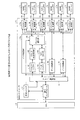
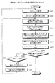
次に、図9を参照して、実施例1の変形例について説明する。図9は、変形例に係るNANDコントローラのブロック図である。
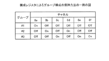
また、NANDコントローラ10側でグループを選択する方法は、優先度を用いる方法に限らない。例えば、処理要求に付加された優先度以外の付随情報を用いてもよい。
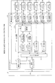
2a,2b メモリ
3 DIMM
4,4a,4b CPU
5 I/Oハブ
6a,6b SSD
8a〜8f チャネル
7,7a〜7f NANDフラッシュメモリ
10,10a,10b NANDコントローラ
11 構成レジスタ
12 通信インタフェース
13 グループ識別部
14a〜14c データ処理部
15a〜15f チャネル制御部
16 構成解析部
141 リクエストバッファ
142 アドレス変換制御部
143 データバッファ
144 RAID制御部
145 チャネル選択部
Claims (8)
- 演算処理部と、
記憶装置を搭載した複数のチャネルと、
前記演算処理部からのデータの処理命令に応じて、前記チャネルを用いて前記記憶装置に対してデータ処理を行う複数のデータ処理部と、
前記チャネルの処理性能を基に重複を許して複数のグループに分けられた前記チャネルのグループ構成及び各前記グループに含まれる前記チャネルを用いてデータ処理を行う前記データ処理部の割り当てを記憶するグループ管理部と、
前記演算処理部からのデータの処理命令を基に、前記グループ管理部が記憶するグループの中からデータ処理を実行させるグループを選択し、選択したグループに割り当てられた前記データ処理部に対してデータ処理を行わせる制御部と
を備えたことを特徴とする情報処理装置。 - 前記演算処理部は、前記グループ管理部が記憶するグループの中からデータ処理の対象とするグループを決定し、決定したグループを指定する前記処理命令を生成し、
前記制御部は、前記演算処理部から前記処理命令を受信し、受信した処理命令により指定されたグループをデータ処理を実行させるグループとする
ことを特徴とする請求項1に記載の情報処理装置。 - 前記演算処理部は、データ処理の優先度を決定し、前記優先度を示す情報を含む前記処理命令を生成し、
前記グループ管理部は、各前記グループに属する前記チャネルの性能情報を記憶し、
前記制御部は、前記演算処理部から前記処理命令を受信し、前記グループ管理部が記憶する性能情報及び前記処理命令で示される前記優先度を基に、データ処理を実行させるグループを選択する
ことを特徴とする請求項1に記載の情報処理装置。 - 前記演算処理部は、付随情報を含む前記処理命令を生成し、
前記制御部は、前記付随情報を基にデータ処理を実行させるグループを選択する
ことを特徴とする請求項1に記載の情報処理装置。 - 前記記憶装置の性能を基に前記チャネルの処理性能を決定し、前記チャネルを複数のグループに分け前記グループ管理部に記憶させるグループ構成部をさらに有することを特徴とする請求項1〜4のいずれか一つに記載の情報処理装置。
- 前記記憶装置は、自己の性能情報を格納しており、
前記グループ構成部は、各前記記憶装置が記憶する性能情報を取得する
ことを特徴とする請求項5に記載の情報処理装置。 - 記憶装置を搭載した複数のチャネルと、
前記チャネルを用いて前記記憶装置に対してデータ処理を行う複数のデータ処理部と、
前記チャネルの処理性能を基に重複を許して複数のグループに分けられた前記チャネルのグループ構成及び各前記グループに含まれる前記チャネルを用いてデータ処理を行う前記データ処理部の割り当てを記憶するグループ管理部と、
データの処理命令を基に、前記グループ管理部が記憶するグループの中からデータ処理を実行させるグループを選択し、選択したグループに割り当てられた前記データ処理部に対してデータ処理を行わせる制御部と
を備えたことを特徴とする記憶装置制御回路。 - 記憶装置を搭載した複数のチャネルの処理性能を基に重複を許して前記チャネルを複数のグループに分け、
前記チャネルを用いて前記記憶装置に対するデータ処理を行う複数のデータ処理回路の中から、各グループに含まれる前記チャネルを用いてデータ処理を行うデータ処理回路を割り当て、
データの処理命令を基に、前記グループの中からデータ処理を実行させるグループを選択し、
選択したグループに割り当てられた前記データ処理回路に対してデータ処理を行わせる
ことを特徴とする記憶装置の制御方法。
Priority Applications (3)
| Application Number | Priority Date | Filing Date | Title |
|---|---|---|---|
| JP2013227724A JP6232936B2 (ja) | 2013-10-31 | 2013-10-31 | 情報処理装置、記憶装置制御回路及び記憶装置の制御方法 |
| US14/471,041 US20150120993A1 (en) | 2013-10-31 | 2014-08-28 | Information processing apparatus, storage device control circuit, and storage device control method |
| EP20140183350 EP2869183A1 (en) | 2013-10-31 | 2014-09-03 | Information processing apparatus, storage device control circuit, and storage device control method |
Applications Claiming Priority (1)
| Application Number | Priority Date | Filing Date | Title |
|---|---|---|---|
| JP2013227724A JP6232936B2 (ja) | 2013-10-31 | 2013-10-31 | 情報処理装置、記憶装置制御回路及び記憶装置の制御方法 |
Publications (2)
| Publication Number | Publication Date |
|---|---|
| JP2015088071A JP2015088071A (ja) | 2015-05-07 |
| JP6232936B2 true JP6232936B2 (ja) | 2017-11-22 |
Family
ID=51492836
Family Applications (1)
| Application Number | Title | Priority Date | Filing Date |
|---|---|---|---|
| JP2013227724A Active JP6232936B2 (ja) | 2013-10-31 | 2013-10-31 | 情報処理装置、記憶装置制御回路及び記憶装置の制御方法 |
Country Status (3)
| Country | Link |
|---|---|
| US (1) | US20150120993A1 (ja) |
| EP (1) | EP2869183A1 (ja) |
| JP (1) | JP6232936B2 (ja) |
Families Citing this family (5)
| Publication number | Priority date | Publication date | Assignee | Title |
|---|---|---|---|---|
| JP6160294B2 (ja) * | 2013-06-24 | 2017-07-12 | 富士通株式会社 | ストレージシステム、ストレージ装置及びストレージシステムの制御方法 |
| CN105653207B (zh) * | 2015-12-31 | 2019-03-01 | 深圳市德名利电子有限公司 | 一种闪存接口信息的实时解析方法和系统 |
| US11294594B2 (en) * | 2017-08-07 | 2022-04-05 | Kioxia Corporation | SSD architecture supporting low latency operation |
| US10922038B2 (en) * | 2018-12-31 | 2021-02-16 | Kyocera Document Solutions Inc. | Memory control method, memory control apparatus, and image forming method that uses memory control method |
| US10764455B2 (en) | 2018-12-31 | 2020-09-01 | Kyocera Document Solutions Inc. | Memory control method, memory control apparatus, and image forming method that uses memory control method |
Family Cites Families (14)
| Publication number | Priority date | Publication date | Assignee | Title |
|---|---|---|---|---|
| JP2000187559A (ja) * | 1998-12-24 | 2000-07-04 | Hitachi Ltd | ディスクシステム |
| JP2004021370A (ja) | 2002-06-13 | 2004-01-22 | Hitachi Ltd | ディスクアレイ制御装置 |
| JP4528551B2 (ja) * | 2004-04-14 | 2010-08-18 | 株式会社日立製作所 | ストレージシステム |
| JP4721734B2 (ja) * | 2005-03-15 | 2011-07-13 | 株式会社日立製作所 | ストレージシステム、及び情報処理システム |
| JP2007188341A (ja) * | 2006-01-13 | 2007-07-26 | Hitachi Ltd | 記憶デバイス制御装置 |
| JP4782825B2 (ja) * | 2006-04-10 | 2011-09-28 | インターナショナル・ビジネス・マシーンズ・コーポレーション | データの保存先を複数のテープ記録装置から選択するための装置、方法及びプログラム |
| JP2007304896A (ja) * | 2006-05-12 | 2007-11-22 | Fujitsu Ltd | チャネルスイッチ装置,ストレージシステムおよびアクセス経路切り替え方法 |
| KR101297563B1 (ko) * | 2007-11-15 | 2013-08-19 | 삼성전자주식회사 | 스토리지 관리 방법 및 관리 시스템 |
| TWI369688B (en) * | 2008-05-21 | 2012-08-01 | Ite Tech Inc | Integrated storage device and controlling method thereof |
| JP5241671B2 (ja) * | 2009-10-05 | 2013-07-17 | 株式会社日立製作所 | 記憶装置のデータ移行制御方法 |
| JP5492731B2 (ja) * | 2010-10-06 | 2014-05-14 | 株式会社日立製作所 | 仮想計算機のボリューム割当て方法およびその方法を用いた計算機システム |
| US8924627B2 (en) * | 2011-03-28 | 2014-12-30 | Western Digital Technologies, Inc. | Flash memory device comprising host interface for processing a multi-command descriptor block in order to exploit concurrency |
| JP2013156929A (ja) * | 2012-01-31 | 2013-08-15 | Toshiba Corp | 記憶装置とその制御方法 |
| CN103049216B (zh) * | 2012-12-07 | 2015-11-25 | 记忆科技(深圳)有限公司 | 固态硬盘及其数据处理方法、系统 |
-
2013
- 2013-10-31 JP JP2013227724A patent/JP6232936B2/ja active Active
-
2014
- 2014-08-28 US US14/471,041 patent/US20150120993A1/en not_active Abandoned
- 2014-09-03 EP EP20140183350 patent/EP2869183A1/en not_active Withdrawn
Also Published As
| Publication number | Publication date |
|---|---|
| EP2869183A1 (en) | 2015-05-06 |
| JP2015088071A (ja) | 2015-05-07 |
| US20150120993A1 (en) | 2015-04-30 |
Similar Documents
| Publication | Publication Date | Title |
|---|---|---|
| US10564872B2 (en) | System and method for dynamic allocation to a host of memory device controller memory resources | |
| US10528464B2 (en) | Memory system and control method | |
| US12287751B2 (en) | Computing system including CXL switch, memory device and storage device and operating method thereof | |
| JP6329318B2 (ja) | 情報処理装置 | |
| CN107908571B (zh) | 一种数据写入方法、闪存装置及存储设备 | |
| CN109101185B (zh) | 固态存储设备及其写命令和读命令处理方法 | |
| CN108877862B (zh) | 页条带的数据组织以及向页条带写入数据的方法与装置 | |
| US11379127B2 (en) | Method and system for enhancing a distributed storage system by decoupling computation and network tasks | |
| US9575914B2 (en) | Information processing apparatus and bus control method | |
| GB2533688A (en) | Resource allocation and deallocation for power management in devices | |
| CN111258496B (zh) | 动态分配数据路径的装置和方法 | |
| JP6232936B2 (ja) | 情報処理装置、記憶装置制御回路及び記憶装置の制御方法 | |
| US20230376217A1 (en) | Storage device, memory device, and computing system including the same | |
| WO2015078193A1 (zh) | 存储空间的管理方法和存储管理装置 | |
| CN110308865B (zh) | 存储器系统、计算系统及其操作方法 | |
| US20250217309A1 (en) | Computing system including cxl switch, memory device and storage device and operating method thereof | |
| CN110321071A (zh) | 存储器系统、其操作方法和包括该存储器系统的计算系统 | |
| JP2018113075A (ja) | 情報処理装置 | |
| US10936534B2 (en) | Converged memory device and method thereof | |
| US20240069814A1 (en) | Storage server and operation method of storage server | |
| US12093174B2 (en) | Methods and apparatus for persistent data structures | |
| KR102433549B1 (ko) | 통합 메모리 디바이스 및 그의 동작 방법 | |
| KR20250022982A (ko) | 메모리 장치 및 이를 포함하는 컴퓨팅 시스템 | |
| US20250245147A1 (en) | Storage device and operation method thereof | |
| KR20250012280A (ko) | 스토리지 시스템 및 이를 포함하는 컴퓨팅 시스템 |
Legal Events
| Date | Code | Title | Description |
|---|---|---|---|
| A621 | Written request for application examination |
Free format text: JAPANESE INTERMEDIATE CODE: A621 Effective date: 20160705 |
|
| A977 | Report on retrieval |
Free format text: JAPANESE INTERMEDIATE CODE: A971007 Effective date: 20170518 |
|
| A131 | Notification of reasons for refusal |
Free format text: JAPANESE INTERMEDIATE CODE: A131 Effective date: 20170606 |
|
| A521 | Request for written amendment filed |
Free format text: JAPANESE INTERMEDIATE CODE: A523 Effective date: 20170731 |
|
| TRDD | Decision of grant or rejection written | ||
| A01 | Written decision to grant a patent or to grant a registration (utility model) |
Free format text: JAPANESE INTERMEDIATE CODE: A01 Effective date: 20170926 |
|
| A61 | First payment of annual fees (during grant procedure) |
Free format text: JAPANESE INTERMEDIATE CODE: A61 Effective date: 20171009 |
|
| R150 | Certificate of patent or registration of utility model |
Ref document number: 6232936 Country of ref document: JP Free format text: JAPANESE INTERMEDIATE CODE: R150 |
|
| S111 | Request for change of ownership or part of ownership |
Free format text: JAPANESE INTERMEDIATE CODE: R313111 |
|
| R350 | Written notification of registration of transfer |
Free format text: JAPANESE INTERMEDIATE CODE: R350 |
|
| R250 | Receipt of annual fees |
Free format text: JAPANESE INTERMEDIATE CODE: R250 |