JP6230258B2 - Image processing apparatus and image processing method - Google Patents
Image processing apparatus and image processing method Download PDFInfo
- Publication number
- JP6230258B2 JP6230258B2 JP2013088705A JP2013088705A JP6230258B2 JP 6230258 B2 JP6230258 B2 JP 6230258B2 JP 2013088705 A JP2013088705 A JP 2013088705A JP 2013088705 A JP2013088705 A JP 2013088705A JP 6230258 B2 JP6230258 B2 JP 6230258B2
- Authority
- JP
- Japan
- Prior art keywords
- image processing
- chip
- data
- image
- processing chip
- Prior art date
- Legal status (The legal status is an assumption and is not a legal conclusion. Google has not performed a legal analysis and makes no representation as to the accuracy of the status listed.)
- Active
Links
Images


Classifications
-
- G—PHYSICS
- G06—COMPUTING; CALCULATING OR COUNTING
- G06K—GRAPHICAL DATA READING; PRESENTATION OF DATA; RECORD CARRIERS; HANDLING RECORD CARRIERS
- G06K15/00—Arrangements for producing a permanent visual presentation of the output data, e.g. computer output printers
- G06K15/40—Details not directly involved in printing, e.g. machine management, management of the arrangement as a whole or of its constitutive parts
- G06K15/4005—Sharing resources or data with other data processing systems; Preparing such data
- G06K15/402—Sharing data concerning the arrangement's configuration or current state
-
- G—PHYSICS
- G06—COMPUTING; CALCULATING OR COUNTING
- G06K—GRAPHICAL DATA READING; PRESENTATION OF DATA; RECORD CARRIERS; HANDLING RECORD CARRIERS
- G06K15/00—Arrangements for producing a permanent visual presentation of the output data, e.g. computer output printers
- G06K15/02—Arrangements for producing a permanent visual presentation of the output data, e.g. computer output printers using printers
- G06K15/18—Conditioning data for presenting it to the physical printing elements
- G06K15/1848—Generation of the printable image
- G06K15/1856—Generation of the printable image characterized by its workflow
- G06K15/1857—Generation of the printable image characterized by its workflow involving parallel processing in the same printing apparatus
-
- G—PHYSICS
- G03—PHOTOGRAPHY; CINEMATOGRAPHY; ANALOGOUS TECHNIQUES USING WAVES OTHER THAN OPTICAL WAVES; ELECTROGRAPHY; HOLOGRAPHY
- G03G—ELECTROGRAPHY; ELECTROPHOTOGRAPHY; MAGNETOGRAPHY
- G03G15/00—Apparatus for electrographic processes using a charge pattern
- G03G15/50—Machine control of apparatus for electrographic processes using a charge pattern, e.g. regulating differents parts of the machine, multimode copiers, microprocessor control
-
- G—PHYSICS
- G06—COMPUTING; CALCULATING OR COUNTING
- G06F—ELECTRIC DIGITAL DATA PROCESSING
- G06F3/00—Input arrangements for transferring data to be processed into a form capable of being handled by the computer; Output arrangements for transferring data from processing unit to output unit, e.g. interface arrangements
- G06F3/12—Digital output to print unit, e.g. line printer, chain printer
- G06F3/1293—Printer information exchange with computer
-
- G—PHYSICS
- G06—COMPUTING; CALCULATING OR COUNTING
- G06F—ELECTRIC DIGITAL DATA PROCESSING
- G06F9/00—Arrangements for program control, e.g. control units
- G06F9/06—Arrangements for program control, e.g. control units using stored programs, i.e. using an internal store of processing equipment to receive or retain programs
- G06F9/46—Multiprogramming arrangements
- G06F9/54—Interprogram communication
-
- G—PHYSICS
- G06—COMPUTING; CALCULATING OR COUNTING
- G06K—GRAPHICAL DATA READING; PRESENTATION OF DATA; RECORD CARRIERS; HANDLING RECORD CARRIERS
- G06K15/00—Arrangements for producing a permanent visual presentation of the output data, e.g. computer output printers
- G06K15/02—Arrangements for producing a permanent visual presentation of the output data, e.g. computer output printers using printers
- G06K15/18—Conditioning data for presenting it to the physical printing elements
-
- G—PHYSICS
- G03—PHOTOGRAPHY; CINEMATOGRAPHY; ANALOGOUS TECHNIQUES USING WAVES OTHER THAN OPTICAL WAVES; ELECTROGRAPHY; HOLOGRAPHY
- G03G—ELECTROGRAPHY; ELECTROPHOTOGRAPHY; MAGNETOGRAPHY
- G03G2215/00—Apparatus for electrophotographic processes
- G03G2215/00016—Special arrangement of entire apparatus
- G03G2215/00021—Plural substantially independent image forming units in cooperation, e.g. for duplex, colour or high-speed simplex
-
- G—PHYSICS
- G06—COMPUTING; CALCULATING OR COUNTING
- G06K—GRAPHICAL DATA READING; PRESENTATION OF DATA; RECORD CARRIERS; HANDLING RECORD CARRIERS
- G06K2215/00—Arrangements for producing a permanent visual presentation of the output data
- G06K2215/0082—Architecture adapted for a particular function
Description
本発明は、複数の画像処理ユニットを用いて画像処理を実行する画像処理装置及び画像処理方法に関する。 The present invention relates to an image processing apparatus and an image processing method for executing image processing using a plurality of image processing units.
従来、画像処理装置では処理性能の向上のため、複数の機能単位を並列に動作させることが行われている。複数の画像処理機能を1つのASICに搭載し、チップ内部で画像処理モジュールを並列に動作させるものや、複数の画像処理チップをチップ外部バスに接続し、チップ単位で並列動作を行うものなどが知られている。しかしながら、複数のチップをバスで接続する場合、バスの転送性能がボトルネックとなって性能が制限される。そこで、ポイント・ツー・ポイント接続の高速シリアルインターフェースであるPCI Express(登録商標、以降PCIeとも記載する)を活用した画像システムが提案されている(特許文献1参照)。特許文献1では、画像処理ユニットを複数接続し、画像処理内容に応じて選択的、並列的に画像処理ユニットを動作させている。
Conventionally, in order to improve processing performance in an image processing apparatus, a plurality of functional units are operated in parallel. There are those in which multiple image processing functions are mounted on one ASIC and the image processing modules are operated in parallel inside the chip, and those in which multiple image processing chips are connected to the chip external bus and are operated in parallel on a chip basis. Are known. However, when a plurality of chips are connected by a bus, the transfer performance of the bus becomes a bottleneck and the performance is limited. In view of this, an image system using PCI Express (registered trademark, hereinafter also referred to as PCIe), which is a high-speed serial interface for point-to-point connection, has been proposed (see Patent Document 1). In
特許文献1では、PCIeインタフェースを持つ複数の画像処理モジュールをPCIeスイッチと呼ばれるデバイスチップを介して接続できるように構成されている。この構成では、処理性能を向上させるために同一機能を持つ画像処理モジュールをPCIeスイッチに複数接続し、並列処理を行う。この場合、PCIeスイッチのポート数を、増設する処理モジュール数に対応させて増やさなければならないため、PCIeスイッチチップの回路規模、端子数がポート数に比例して大きくなってしまう。
In
また、特許文献1では、複数の画像処理モジュールを用いて1ページの画像データを主走査方向に分割し、各処理モジュールで分散して並列処理する例が開示されている。しかしながら、このような方法で画像処理を分割する場合、高速化のために処理モジュール数を増加させると、主走査方向の分割数も増加するため、入力画像データの分割方法、処理後の画像データの結合方法が複雑化する。
本発明は、上記課題に鑑みてなされたものであり、スケーラブルに処理能力の向上が可能な画像形成装置及び画像処理方法を提供することを目的としている。 SUMMARY An advantage of some aspects of the invention is that it provides an image forming apparatus and an image processing method capable of improving processing capability in a scalable manner.
上述のような課題を解決するための本発明の画像形成装置は、入力された画像データに画像処理を実行する、第1の画像処理チップと第2の画像処理チップとを備え、前記第1の画像処理チップと前記第2の画像処理チップとは、直列に接続されており、前記第1の画像処理チップと前記第2の画像処理チップのそれぞれはは、転送手段と画像処理手段とを備え、前記第1の画像処理チップの前記画像処理手段は、入力された第1の画像データに所定の画像処理を実行して第2の画像データを生成し、前記第1の画像処理チップの前記転送手段は、入力された第1の画像データを画像処理せずに転送し且つ前記第2の画像データを転送し、前記第1の画像処理チップ及び前記第2の画像処理チップの各画像処理手段は、画像データから量子化データを生成する第1画像処理部と、量子化データから印刷データを生成する第2画像処理部と、のうち少なくともいずれかを備え、前記第1画像処理部により生成された量子化データは、次の画像処理チップへ転送され、前記第2画像処理部により生成された印刷データは、印刷手段へ転送される。 The image forming apparatus of the present invention to solve the problems as described above, executes an image processing on input image data, comprising: a first image processing chip and a second image processing chip, said first The image processing chip and the second image processing chip are connected in series, and each of the first image processing chip and the second image processing chip includes a transfer unit and an image processing unit. And the image processing means of the first image processing chip performs predetermined image processing on the input first image data to generate second image data, and the first image processing chip The transfer means transfers the input first image data without image processing and transfers the second image data, and each image of the first image processing chip and the second image processing chip is transferred. Processing means quantize from image data At least one of a first image processing unit that generates data and a second image processing unit that generates print data from the quantized data, and the quantized data generated by the first image processing unit is The print data transferred to the next image processing chip and generated by the second image processing unit is transferred to the printing means .
本発明によれば、画像処理ユニット数を増やすことで、スケーラブルに処理性能を向上させることが可能な画像処理システム及び画像処理方法を実現することができる。 According to the present invention, it is possible to realize an image processing system and an image processing method capable of improving processing performance in a scalable manner by increasing the number of image processing units.
以下、本発明の実施の形態について詳細に説明する。 Hereinafter, embodiments of the present invention will be described in detail.
(実施形態1)
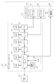
図1は、本実施形態に係る画像処理システムの一例としてのプリンタシステムの構成を示すブロック図である。
(Embodiment 1)
FIG. 1 is a block diagram illustrating a configuration of a printer system as an example of an image processing system according to the present embodiment.
図1に示すように、プリンタシステムでは、画像処理装置であるプリンタ101がLANやUSBなどのインタフェースを介してホストPC100と接続されている。
As shown in FIG. 1, in the printer system, a
プリンタ101は、プリンタコントローラ102と、プリンタエンジン103と、を備える。プリンタコントローラ102は、ホストPC100から受信した印刷ジョブを処理し、印刷メディアへ印刷する印刷データを生成し、その印刷データをプリンタエンジン103へ送信する。プリンタエンジン103は、適切なタイミング制御を行い、各モータを駆動し、プリンタコントローラ102で生成された印刷データを用いて印刷メディア上(被記録媒体上)にインク(記録剤)により画像を形成する。
The
プリンタコントローラ102は、ホストPC100と接続するインタフェースチップ104と、複数の画像処理ユニットと、を備えている。そして、画像処理ユニットとして、インタフェースチップ104から入力される入力画像データを処理する画像処理チップ109及び111と、画像処理チップ109及び111から入力されたデータを処理するエンジンチップ113及び115と、を備える。本実施形態では、各画像処理チップは、インタフェースチップ104から転送された多値画像データから二値画像データ(量子化データ)を生成し、各エンジンチップへ出力する。また、各エンジンチップは、画像処理チップから転送された二値画像データからプリントヘッドへ出力する印刷データを生成し、プリントヘッド(プリントヘッドA118及びプリントヘッドB119)へ印刷データを出力する。
The
インタフェースチップ104は、RAM106、ROM105、操作パネル107、HDD108が接続されており、また、プリンタエンジン103のエンジン制御部120と接続されている。さらに、インタフェースチップ104は、1つの画像処理チップ(IP−A109)に接続されている。
The
ROM105は、プリンタコントローラ102の制御手順、処理手順等を保持している。
The
操作パネル107は、使用者による入力処理を行うものであり、ホストPC100に対する指示や設定を行う。本実施形態では、操作パネル107としたが、キーボード、ポインティングデバイス等の他の入力装置からなるものであってもよい。
The
本実施形態では、プリンタコントローラ102は、画像処理チップとして同じタイプのチップであるIP−A109とIP−B111の2個を備える。具体的には、IP−A109とIP−B111が直列に接続されており、IP−A109がインタフェースチップ104にIP−A109が接続されている。すなわち、インタフェースチップ104に画像処理チップIP−A109が、画像処理チップIP−A109に画像処理チップIP−B111チップが順次接続されている。このように、プリンタコントローラ102は、画像処理チップを直列に接続した処理部群を備えている。そして、図1に示すように、IP−A109チップにはRAM110、IP−B111チップにはRAM112が接続されている。
In the present embodiment, the
また、本実施形態では、プリンタコントローラ102は、エンジンチップとして同じタイプのチップであるE−A113とE−B115の2個を備える。具体的には、E−A113とE−B115が直列に接続されており、E−A113がIP−B111に接続されている。すなわち、IP−B111にE−A113チップが、E−A113チップにE−B115チップが順次接続されている。このように、プリンタコントローラ102は、エンジンチップを直列に接続した処理部群を備えている。そして、図1に示すように、E−A113チップにRAM114とプリントヘッドA118が接続され、E−B115チップにRAM116とプリントヘッドB119が接続されている。このように、各エンジンチップは、それぞれ異なるプリントヘッドに接続されている。
In the present embodiment, the
上述したように、プリンタコントローラ102は、複数の画像処理チップ、複数のエンジンチップをそれぞれ、2つのチップ間インタフェースを相互に接続することにより、直列(以下、縦列ともいう)に接続した構成となっている。ホストPC100から送付された印刷データはインタフェースチップ104で受信され、順次画像処理チップ(IP−A109、IP−B111)へ転送されて画像処理を実施し、次にエンジンチップ(E−A113、E−B115)へ転送される。そして、エンジンチップにおいてさらに画像処理を実施して印刷データへ変換され、プリントヘッドへ送られる。
As described above, the
プリンタエンジン103は、プリントヘッドを搭載したキャリッジ117と、エンジン制御部120と、図示しない駆動モータ、印刷メディア搬送機構、インク供給系を含む。
The
キャリッジ117は、2つのプリントヘッド(プリントヘッドA118及びプリントヘッドB119)を搭載し、プリントヘッドA118、プリントヘッドB119は、それぞれエンジンチップE−A113、E−B115と接続されている。各プリントヘッドは、エンジンチップから出力される印刷データを受けて、図示しないヘッドノズル部からインクを吐出する。吐出されたインクが印刷メディアへ着弾し、画像を形成する。
The
エンジン制御部120は、制御信号により、キャリッジ117、図示しない駆動モータ、印刷メディア搬送機構を適切なタイミングで駆動させる。
The
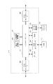
図2は、本実施形態におけるインタフェースチップ104の内部構成を示すブロック図である。
FIG. 2 is a block diagram showing an internal configuration of the
図2に示すように、クロスバースイッチ202には各種機能ブロックが接続され、相互に通信が可能な構成となっている。プリンタ101は、ホストPCと通信するインタフェースとして、LAN、USBを備え、それぞれインタフェースチップ104のLANコントローラ200、インタフェースチップ104のUSBコントローラ201が制御を行う。
As shown in FIG. 2, various functional blocks are connected to the
インタフェースチップ104は、CPUコア203、ROMコントローラ204に接続されるROM105、RAMコントローラ205に接続されるRAM106、HDDコントローラ209に接続されるHDD108によってチップ内部制御を行う。
The
操作パネル107は、操作パネルコントローラ206を介してクロスバースイッチ202に接続される。
The
また、インタフェースチップ104は、DMAコントローラ207、復号部208によってデータ通信処理を行う。
The
エンジン制御部インタフェース210は、プリンタエンジン103に接続され、キャリッジ117や図示しない駆動モータ、印刷メディア搬送機構を駆動するタイミング制御信号を出力する。
The engine
PCIeコントローラ211は、画像処理チップと他のチップ間の接続インタフェースであるPCIeの通信制御を行う。PCIeコントローラ211はルートコンプレックス動作を行う。PCIeコントローラ211は、PCI Express規格(PCIe)のインターフェースである。なお、本実施形態では、画像処理チップと他のチップとの接続のためにポイント・ツー・ポイント接続の高速シリアルインターフェースであるPCIeを用いたがこれに限定されるものではなく、その他のインタフェースであってもよい。
The
インタフェースチップ104では、CPUコア203がROM105あるいはHDD108に格納されたプログラムに従って動作する。
In the
また、ホストPCから入力された通信データ(画像データ)は、LANコントローラ200又はUSBコントローラ201を経由して、RAM106へ格納し、CPUコア203によって通信プロトコル処理を実施し、HDD108へ格納する。圧縮された画像データを受信した場合は、復号部208を使って復号処理を行い、RAM106へ格納する。復号後の入力画像データは、DMAコントローラ207によって読み出され、PCIeコントローラ211を通して画像処理チップへと転送される。
Communication data (image data) input from the host PC is stored in the
また、ユーザにより操作パネル107を介してプリンタの電源制御やプリンタの動作設定の指示が行われる。操作パネル107におけるボタン操作やキー操作は操作パネルコントローラ206で受けた後、割り込みによってCPUコア203へ伝えられ、対応する処理が行われる。
Also, the user gives instructions for printer power control and printer operation settings via the
図3は、本実施形態における画像処理チップであるIP−A109の内部構造を示すブロック図である。本実施形態では、プリンタコントローラ102には同じ画像処理チップが2つ搭載されており、それぞれIP−A109、IP−B111である。なお、ここでは、IP−A109について説明するが、IP−B111も同じ内部構造を持つ。
FIG. 3 is a block diagram showing the internal structure of IP-
IP−A109は、クロスバースイッチ301に各種機能ブロックが接続され、各種機能ブロックが相互に通信可能な構成となっている。PCIeコントローラA300は前段のチップとのインタフェース制御を行う。また、PCIeコントローラA300は、エンドポイントモードで動作し、インタフェースチップ104のルートコンプレックスモードで動作するPCIeコントローラ211と接続される。
The IP-
画像処理チップIP−A109は、CPUコア302、ROM304、RAMコントローラ303に接続するRAM110によってチップ内部制御を行う。IP−A109は、CPUコア302がROM304に格納されたプログラムに従って動作する。ROM304は、IP−A109に内蔵され、図示しないROMコントローラによって制御される。また、RAM110は、RAMコントローラ303によって制御される。
The image processing chip IP-
PCIeコントローラB308は、次段のチップであるIP−B111とのインタフェース制御を行う。PCIeコントローラB308は、ルートコンプレックスモードで動作する。 The PCIe controller B308 performs interface control with the IP-B111, which is the next chip. The PCIe controller B308 operates in the root complex mode.
転送処理部306は、CPUコア302からの指示に従って、RAM110に格納されているデータを読み出し、PCIeコントローラB308を経由して、次段のチップの所定アドレスに対してデータを転送する。
The
画像処理部307は、CPUコア302からの指示に従って、RAM110から画像データを読み出して、画像処理を行い、画像処理後のデータを処理結果として次段のチップの所定アドレスに対して転送する。インタフェースチップ104から送信された入力画像データは、PCIeコントローラA300を経由して、RAM110へ格納される。CPUコア302は、前段のチップからデータ転送完了通知を受け、接続チップ構成に従ってあらかじめ決定されたデータ処理の実行制御を行う。ここでいうデータ処理とは、画像処理を行って次段のチップへ転送する転送処理と、画像処理を行わずに次段のチップへ転送する転送処理である。
The
画像処理部307は、入力ガンマ補正、色空間変換、出力ガンマ補正、二値化処理などの各種画像処理を行う回路を実装している。この画像処理部307は、これらの回路、言い換えれば、これらの機能回路ブロックを複数系統備え、同時並列に多色処理を行うことができる。本実施形態では、入力画像データは、RGB各色10ビット階調であり、画像処理部307は、色空間変換処理によって、入力画像データをインク色へ分解し、二値化処理を行う。例えば、機能回路ブロックを4系統備えることにより、最大CMYK4色へ展開し、処理することが可能となる。そして、各回路が備えるレジスタに所定の設定を行うことにより、同時処理可能なインク色数を1〜4色の間で設定可能となる。
The
なお、画像処理チップIP−B111は、上述したようにIP−A109と同様の構成からなり、IP−A109と同様に動作する。画像処理チップIP−B111は、前段がインタフェースチップ104ではなく、画像処理チップIP−A109に接続され、次段はエンジンチップE−A113が接続される。
Note that the image processing chip IP-
図4は、本実施形態におけるエンジンチップE−A113の内部構造を示すブロック図である。本実施形態では、プリンタコントローラ102には同じエンジンチップが2つ搭載されており、それぞれエンジンチップE−A113、E−B115である。なお、ここでは、E−A113について説明するが、E−B115も同じ内部構造を持つ。
FIG. 4 is a block diagram showing the internal structure of the
E−A113は、クロスバースイッチ401に各種機能ブロックが接続され、各種機能ブロックが相互に通信可能な構成となっている。E−A113は、CPUコア402、ROM404、RAMコントローラ403に接続されるRAM114によってチップ内部制御を行う。具体的には、エンジンチップE−A113は、CPUコア402がROM404に格納されたプログラムに従い動作する。ROM404は、E−A113に内蔵され、図示しないROMコントローラによって制御される。また、RAM114は、RAMコントローラ403によって制御される。
The
PCIeコントローラC400は、エンドポイントモードで動作し、前段のチップ(画像処理チップIP−B11)のルートコンプレックスモードで動作するPCIeコントローラB308と接続される。 The PCIe controller C400 operates in the endpoint mode and is connected to the PCIe controller B308 that operates in the root complex mode of the preceding chip (image processing chip IP-B11).
PCIeコントローラD408は、後段のチップ(エンジンチップE−B115)とのインタフェース制御を行う。PCIeコントローラD408は、ルートコンプレックスモードで動作する。 The PCIe controller D408 performs interface control with a subsequent chip (engine chip E-B115). The PCIe controller D408 operates in the root complex mode.
ヘッドデータ転送部409は、プリントヘッドA118に対してヘッドデータを転送する。
The head
転送処理部406はCPUコア402からの指示に従って、RAM114に格納されているデータを読み出し、PCIeコントローラD408を経由して、次段のチップの所定アドレスに対してデータを転送する。二値画像処理部407は、CPUコア402からの指示に従って、RAM114から画像データを読み出して二値画像処理を行い、画像処理後のデータを処理結果としてRAM114へ書き戻す。画像処理チップIP−B111から送信された二値画像データはPCIeコントローラC400を経由して、RAM114へ格納される。
The
CPUコア402は、前段のチップ(本実施形態では、IP−B111)からデータ転送完了通知を受け、接続チップ構成に従ってあらかじめ決定されたデータ処理の実行制御を行う。ここでいうデータ処理とは、画像処理を行って次段のチップへ転送する処理と、画像処理を行わずに次段のチップへ転送する処理、及び画像処理後のデータをプリントヘッドA118へ転送する処理である。
The
二値画像処理部407は、二値画像データに対してスムージング処理などの各種画像処理を行う回路を実装している。また、これら回路ブロックを複数系統備え、同時並列に画像処理を行うことができる。例えば、回路ブロックを4系統備えることにより、CMYK4色の各色を並列処理可能である。さらに、各画像処理回路が備えるレジスタに所定の設定を行うことにより、同時処理可能な色数を1〜4色の間で設定可能である。
The binary
なお、エンジンチップE−B115は、上述したようにE−A113と同様の構成からなり、同様に動作する。エンジンチップE−B115は、前段が画像処理チップIP−B111ではなく、E−A113に接続される。
The
図5は、画像処理チップ(IP−A109,IP−B111)、エンジンチップ(E−A113,E−B115)の各チップにおけるチップ内部のアドレスマップの例を示したものである。図5では、アドレスを16進数(0x)で4桁に区切って表現している。
FIG. 5 shows an example of an address map inside the chip in each of the image processing chip (IP-
0x0000_0000〜0x7FFF_FFFFまでの領域をRAM領域501に割り当て、各チップに接続されたRAMにアクセス可能である。例えば、IP−A109であればRAM110、E−B115であればRAM116にアクセス可能である。
An area from 0x0000 — 0000 to 0x7FFF_FFFF is allocated to the RAM area 501, and the RAM connected to each chip can be accessed. For example, the IP-
また、0x8000_0000〜0xBFFF_FFFFまでのIO領域(インプットアウトプット領域)は、いわゆる接続領域である。本実施形態では、0x8000_0000〜0x9FFF_FFFFまでの領域を次段チップアドレスA502に割り当て、0xA0000_0000〜0xBFFF_FFFFまでの領域を次段チップアドレスB503に割り当てている。これらのアドレスにアクセスすることで次段に接続されているチップにアクセス可能である。 The IO area (input / output area) from 0x8000 — 0000 to 0xBFFF_FFFF is a so-called connection area. In the present embodiment, an area from 0x8000 — 0000 to 0x9FFF_FFFF is assigned to the next stage chip address A502, and an area from 0xA0000 — 0000 to 0xBFFF_FFFF is assigned to the next stage chip address B503. By accessing these addresses, the chip connected to the next stage can be accessed.
次段チップアドレスA502は次段チップが使用するデータを転送するための領域として使用する。一方、次段チップアドレスB503は次段チップが使用しないデータを転送するための領域として使用する。前段の「次段チップアドレスA502」から転送されたデータは、後述するバッファ領域A506へ転送される。前段の「次段チップアドレスB503」から転送されたデータは、後述するバッファ領域B507へ転送される。 The next-stage chip address A502 is used as an area for transferring data used by the next-stage chip. On the other hand, the next stage chip address B503 is used as an area for transferring data not used by the next stage chip. The data transferred from the “next-stage chip address A502” in the previous stage is transferred to a buffer area A506 described later. The data transferred from the “next-stage chip address B503” in the previous stage is transferred to a buffer area B507 described later.
次段チップアドレスB503は、例えば、画像処理チップIP−A109からエンジンチップE−A113へ二値化処理後のデータを転送する場合に、IP−B111が使用しないデータをIP−B111へ転送するための領域として使用する。この場合のIP−B111が使用しないデータは、IP−A109の二値化処理後のデータである。IP−A109とE−A113の間に接続されているIP−B111は、IP−A109の次段チップアドレスB503から転送されたIP−A109の二値化処理後のデータは自身では使用しないため、加工せずにE−A113へ転送する。
The next-stage chip address B503 is, for example, for transferring data not used by the IP-
0xC000_0000〜0xDFFF_FFFFまでの領域は各チップの内部回路制御・設定用のレジスタ群が配置されているレジスタ領域504である。内部回路に所望の動作をさせるための設定を行う。 An area from 0xC000 — 0000 to 0xDFFF_FFFF is a register area 504 in which a register group for internal circuit control / setting of each chip is arranged. Settings are made to cause the internal circuit to perform a desired operation.
0xE000_0000〜0xFFFF_FFFFまでの領域はROM領域505である。ここでいうROMは、各チップの内部に実装されているROMであり、格納されているプログラムや設定データに従い、各チップが動作する。 An area from 0xE000 — 0000 to 0xFFFF_FFFF is a ROM area 505. The ROM here is a ROM mounted inside each chip, and each chip operates in accordance with stored programs and setting data.
また、RAM領域501内には、2つのバッファ領域(バッファ領域A506及びバッファ領域B507)を設ける。バッファ領域A506は、チップが使用するデータを格納するための領域として使用する。すなわち、バッファ領域A506には、前段チップの次段チップアドレスA502から転送されたデータを格納する。なお、バッファ領域A506へ格納されたデータをチップ自身で画像処理に使用するかどうかは予め設定されており、設定に従って各チップの画像処理部が動作する。バッファ領域B507はそのチップ自身では使用せず、次のチップでのみ使用するデータを格納するための領域として使用する。すなわち、バッファ領域B507には、前段チップの次段チップアドレスB503から転送されたデータを格納する。 In the RAM area 501, two buffer areas (buffer area A506 and buffer area B507) are provided. The buffer area A506 is used as an area for storing data used by the chip. In other words, the buffer area A506 stores the data transferred from the next chip address A502 of the previous chip. Note that whether or not the data stored in the buffer area A506 is used for image processing by the chip itself is set in advance, and the image processing unit of each chip operates according to the setting. The buffer area B507 is not used by the chip itself, but is used as an area for storing data used only by the next chip. In other words, the buffer area B507 stores data transferred from the next chip address B503 of the previous chip.
チップ間のアドレスマップは、各チップのアドレスマップにおいて、前段チップの次段チップアドレスA502は、次段チップのアドレスマップのバッファ領域A506へアクセス可能なように割り当てられている。また前段チップの次段チップアドレスB503は、次段チップのアドレスマップのバッファ領域B507にアクセス可能なように割り当てられている。このようなアドレスの割り当てが可能な機構を、各チップのPCIeコントローラが備えている。 In the address map between chips, in the address map of each chip, the next-stage chip address A502 of the previous-stage chip is assigned so as to be accessible to the buffer area A506 of the next-stage chip address map. The next-stage chip address B503 of the previous-stage chip is assigned so that the buffer area B507 of the address map of the next-stage chip can be accessed. The PCIe controller of each chip has a mechanism capable of such address assignment.
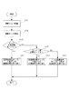
図6は、各画像処理チップでデータ処理を行う色を割り当てる方法の一例を示すフローチャートである。この処理はインタフェースチップ104により実行される。
FIG. 6 is a flowchart illustrating an example of a method for assigning colors for data processing in each image processing chip. This process is executed by the
S101では、ホストPC100から送信された印刷ジョブを受信する。具体的には、画像処理チップは、インタフェースチップ104のホストインタフェースであるLANコントローラ200又はUSBコントローラ201から印刷ジョブを受信する。
In S101, the print job transmitted from the
次に、S102では、印刷モードの解析を行う。具体的には、受信した印刷ジョブの内容を解析し、印刷インク色数、印刷解像度、印刷速度等の印刷モードを決定し、各画像処理チップでデータ処理を行う色の割り当てを決定する。 In step S102, the print mode is analyzed. Specifically, the contents of the received print job are analyzed, the print mode such as the number of print ink colors, the print resolution, the print speed, and the like are determined, and the assignment of colors for data processing in each image processing chip is determined.
S103は、インク6色を使用するモードかどうかを判定する。6色を使用する場合は、S104へ進む。そうでなければS105へ進む。 In step S103, it is determined whether or not the mode uses six ink colors. When using 6 colors, the process proceeds to S104. Otherwise, the process proceeds to S105.
S104は、各画像処理チップに3色ずつの画像処理を割り当てる。図1を用いて説明した通り、画像処理チップIP−A109、画像処理チップIP−B111は、それぞれ最大4色同時に画像処理が可能である。本実施形態では、画像処理チップIP−A109、画像処理チップIP−B111にそれぞれ3色の画像処理を割り当てる。すなわち、画像処理チップIP−A109及び画像処理チップIP−B111で計6色の画像処理を行う。
In S104, image processing of three colors is assigned to each image processing chip. As described with reference to FIG. 1, the image processing chip IP-
S105は、インク4色を使用するモードかどうかを判定する。4色を使用する場合は、S106へ進む。そうでなければ、S107へ進む。 In S105, it is determined whether or not the mode uses four ink colors. If four colors are used, the process proceeds to S106. Otherwise, the process proceeds to S107.
S106は、各画像処理チップに2色ずつの画像処理を割り当てる。本実施形態では、画像処理チップIP−A109、画像処理チップIP−B111にそれぞれ2色の画像処理を割り当てる。すなわち、画像処理チップIP−A109及び画像処理チップIP−B111で計4色の画像処理を行う。
In step S106, image processing of two colors is assigned to each image processing chip. In the present embodiment, two color image processing is assigned to each of the image processing chip IP-
S107は、一つの画像処理チップに1色の画像処理を割り当てる。本実施形態では、インク6色印刷モード及びインク4色印刷モードのいずれでもない場合、図1の画像処理チップIP−A109に1色を割り当て、画像処理チップIP−B111には画像処理する色を割り当てない。1色のみ用いるケースとしては、例えば、黒インクのみを使うモノクロモードなどが挙げられる。画像処理チップIP−B111は画像処理を行わず、後段のエンジンチップが使用するデータを転送する転送処理のみを行う。
In S107, one color image processing is assigned to one image processing chip. In this embodiment, when neither the ink 6-color printing mode nor the ink 4-color printing mode is used, one color is assigned to the image processing chip IP-
上述したように、画像処理チップ1個あたりに割り当てる色数を減らすことによって、画像処理チップ1個あたりの画像処理量を減らし、プリンタとしての高速化、高解像度化を実現することができる。すなわち、画像処理チップを複数個接続し、画像処理チップ1個あたりの画像処理量を減らすことにより、バス使用効率を向上させることができる。これにより、全体としての処理速度を高速化することができる。 As described above, by reducing the number of colors assigned to each image processing chip, the amount of image processing per image processing chip can be reduced, and higher speed and higher resolution as a printer can be realized. That is, the bus use efficiency can be improved by connecting a plurality of image processing chips and reducing the amount of image processing per image processing chip. Thereby, the processing speed as a whole can be increased.
また本実施形態では、各画像処理チップには処理色数が均等になるように割り当てた。例えば、インク6色モード(例えば、高画質モード)の場合、各画像処理チップに3色を割り当てて、標準画質モードの場合は4色を使い、S106のように2色を割り当てた。また、モノクロ高解像度印刷モードの場合は、黒色1色を1個の画像処理チップに割り当てた。これにより、各画像処理チップの処理量が同程度となることにより、いずれかの画像処理チップによる画像処理がボトルネックになることなく、高速、高解像度で印刷することができる。 In this embodiment, each image processing chip is assigned so that the number of processing colors is equal. For example, three colors are assigned to each image processing chip in the ink six-color mode (for example, high image quality mode), four colors are used in the standard image quality mode, and two colors are assigned as in S106. In the monochrome high-resolution printing mode, one black color is assigned to one image processing chip. As a result, the processing amount of each image processing chip becomes approximately the same, so that image processing by any one of the image processing chips can be printed at high speed and high resolution without becoming a bottleneck.
なお、ここでは、画像チップについて説明したが、エンジンチップは、使用するインク色のみをイネーブルにして処理を行う。 Although the image chip has been described here, the engine chip performs processing by enabling only the ink color to be used.
図7は図1のチップ構成において、各チップが取り扱うデータの種別とデータをどのチップからどのチップへ送信するかを示した概略図である。本実施形態では、画像処理チップIP−A109、画像処理チップIP−B111、エンジンチップE−A113、E−B115の各チップは各々4色の画像データを並列処理可能な回路ブロックを搭載している。各チップは最大4色の処理が可能であるが、図6では各チップに2色の処理を割り当てた場合について説明する。
FIG. 7 is a schematic diagram showing the type of data handled by each chip and which chip transmits data to which chip in the chip configuration of FIG. In this embodiment, each of the image processing chip IP-
まず、インタフェースチップ104は図示しないホストPC100から印刷データを受信し、通信用の各種プロトコル処理後、圧縮されているデータを復号したデータを生成する。このデータは、RGB色空間の多値階調データである。図7ではRGBデータをデータ1として示す。
First, the
データ1は、画像処理チップIP−A109、画像処理チップIP−B111で使用される。図7に示すように、データ1は、まず、インタフェースチップ104から画像処理チップIP−A109へ転送され、また、インタフェースチップ104から画像処理チップIP−A109を経由して画像処理チップIP−B11へ転送される。
データ1は、画像処理チップIP−A109で使用するデータなので、インタフェースチップ104の次段チップアドレスA領域502へ転送され、画像処理チップIP−A109のバッファ領域A506に格納される。画像処理チップIP−A109では、データ1(RGBデータ)を画像処理し、インク色空間のインク色データの二色(シアンC、マゼンタM)の二値画像データであるデータ2を生成する。
Since
データ2は、画像処理チップIP−B111へ転送されるが、IP−B111では使用されずに、エンジンチップE−A113へ転送される。したがって、データ2は画像処理チップIP−A109の次段チップアドレスB503領域へ転送され、画像処理チップIP−B111のバッファ領域B507に格納される。
さらに、上述したように、データ1は、インタフェースチップ104から画像処理チップIP−A109を経由して画像処理チップIP−B111へ転送される。すなわち、画像処理チップIP−A109は、データ2を生成する処理を行うと共に、データ1を画像処置チップIP−B111へそのまま転送する処理も行う。データ1は、画像処理チップIP−B111で使用するデータなので画像処理チップIP−A109の次段チップアドレスA502領域へ転送され、画像処理チップIP−B111のバッファ領域A506に格納される。
Further, as described above, the
画像処理チップIP−B111は受信したデータ1を画像処理し、インク色空間のコンポーネントデータの二色(イエローY、ブラックBK)の二値画像データであるデータ3を生成する。データ3はエンジンチップE−A113へ転送されるが、E−A113では使用されずに、エンジンチップE−B115へ転送される。このように、データ3は、エンジンチップE−A113では使用されないので、画像処理チップIP−B111の次段チップアドレスB503領域へ転送され、エンジンチップE−A113のバッファ領域B507へ格納される。一方、画像処理チップIP−A109から受信したデータ2は、エンジンチップE−A113で使用するデータなので、画像処理チップIP−B111の次段チップアドレスA領域へ転送され、エンジンチップE−A113のバッファ領域A506に格納される。
The image processing chip IP-
エンジンチップE−A113は、データ2を画像処理し、ヘッド用データを生成し、図示しない118プリントヘッドA118へ転送する。さらに、エンジンチップE−A113は、データ3をエンジンチップE−B115へ転送する処理も行う。データ3はエンジンチップE−A113の次段チップアドレスA領域へ転送され、エンジンチップE−B115のバッファ領域506へ転送される。
The
エンジンチップE−B115は、データ3を画像処理し、ヘッド用データを生成し、図示しない119プリントヘッドB119へ転送する。
The
上述したようにインタフェースチップ104から出力した入力画像データを画像処理チップIP−A109、画像処理チップIP−B111、エンジンチップE−A113、エンジンチップE−B115で分散・並列生成処理する。より具体的には、入力画像データを各画像処理チップ(IP−A109,IP−B111)に転送し、インク色毎に各画像処理チップの処理を分散して並列処理する。そして、各画像処理チップから得られた二値画像データ(量子化データ)を対応する各エンジンチップ(E−A113,E−B115)に転送し、各エンジンチップで二値画像データの並列処理を行う。最後に、生成したヘッドデータをプリントヘッドへ供給することにより画像を形成できる。このように、本実施形態では、インタフェースチップ104から出力した入力画像データを他のチップを経由して特定のチップへ転送する。
As described above, the input image data output from the
本実施形態では、画像処理チップが、前段のチップから受信したデータを自身の画像処理回路で処理する機能と、前段のチップから受信したデータを次段のチップへ転送する機能と、を備えるものとした。同様に、エンジンチップが、前段のチップから受信したデータを自身の回路で処理する機能と、前段のチップから受信したデータを次段のチップへ転送する機能と、を備えるものとした。そして、画像処理チップ及びエンジンチップを高速なチップ間インタフェースを使って縦列にそれぞれ複数個接続し、インク色データを各チップで分散・並列処理することができる構成とした。 In this embodiment, the image processing chip has a function of processing data received from the previous chip by its own image processing circuit and a function of transferring data received from the previous chip to the next chip. It was. Similarly, the engine chip has a function of processing data received from the preceding chip by its own circuit and a function of transferring data received from the preceding chip to the next chip. A plurality of image processing chips and engine chips are connected in a column using a high-speed inter-chip interface, and the ink color data can be distributed and processed in parallel by each chip.
これにより、バスの使用効率を高めた並列処理を実現することができ、安価に画像形成システムを構成できる。インタフェースチップに各チップを並列につなぐ場合、処理能力を向上させるためにチップ数を増やすと、PCIeスイッチチップの端子数、回路規模、ポート数が増加してしまう。これに対し、本実施形態では、従来のように、画像処理モジュールに相当する画像処理チップを複数個接続するためのスイッチチップを使用する必要がない。また、画像処理チップの数が増加しても、2ポートのPCIeインタフェースを隣接チップで接続することにより、スイッチチップのピン数増加によるコストアップを回避することができる。また、従来のように、処理モジュール数の増加に伴って、複雑な状況判断を伴った制御をする必要がなく、処理モジュール数に対して単純にスケーラブルな回路とすることができる。 As a result, parallel processing with improved bus use efficiency can be realized, and an image forming system can be configured at low cost. When each chip is connected in parallel to the interface chip, if the number of chips is increased in order to improve processing capability, the number of terminals, circuit scale, and number of ports of the PCIe switch chip will increase. On the other hand, in this embodiment, it is not necessary to use a switch chip for connecting a plurality of image processing chips corresponding to the image processing module as in the prior art. Further, even if the number of image processing chips increases, it is possible to avoid an increase in cost due to an increase in the number of pins of the switch chip by connecting a two-port PCIe interface with an adjacent chip. Further, unlike the conventional case, it is not necessary to perform control with complicated situation determination as the number of processing modules increases, and the circuit can be simply scalable with respect to the number of processing modules.
すなわち、本実施形態の画像処理システムは、処理性能を向上させるために画像処理チップ数を増やす際、システムの回路規模、端子数がチップ数に比例して増大することがなく、処理性能とチップ数をスケーラブルに変更可能なものである。言い換えれば、各チップの処理能力を、画像処理において必要とされる最高の処理能力に合わせる必要がなく、チップの処理性能及びチップ数を適宜選択して、所望の処理を実行させることができる。したがって、安価に拡張性の高い画像処理システム及び画像処理方法を実現することができる。 That is, in the image processing system of this embodiment, when the number of image processing chips is increased in order to improve the processing performance, the circuit scale and the number of terminals of the system do not increase in proportion to the number of chips. The number can be changed to be scalable. In other words, it is not necessary to match the processing capability of each chip to the highest processing capability required in image processing, and desired processing can be executed by appropriately selecting the processing performance and the number of chips. Accordingly, it is possible to realize an image processing system and an image processing method that are inexpensive and highly scalable.
また、上述した通り、本実施形態では、画像処理チップが、受信したデータ(入力されたデータ)のうち一部を自身で使用し、使用しないものはそのままの状態で次の画像処理回路へ転送する。このような構成とすることにより、同じ構成からなる画像処理チップを複数接続して、それぞれ異なる画像データや異なる画像処理を実行させることにより、所望の画像処理を行うことができる。また、用途に応じて、画像処理チップに実行させる処理内容を変更することができる。 Further, as described above, in this embodiment, the image processing chip uses a part of the received data (input data) by itself and transfers the unused data as it is to the next image processing circuit. To do. With such a configuration, desired image processing can be performed by connecting a plurality of image processing chips having the same configuration and executing different image data and different image processing. Further, the processing content to be executed by the image processing chip can be changed according to the application.
(他の実施形態)
以上、実施形態を用いて本発明の説明をしたが、本発明の基本的構成は上述したものに限定されるものではない。例えば、実施形態1では、図6に示すステップ内では、具体的なインク色数を示したが、これに限定されるものではなく、インク色数は、実際のプリンタにおいては搭載するインク色数、実装する印刷モードの使用色数によって適宜変更すればよい。
(Other embodiments)
Although the present invention has been described above using the embodiment, the basic configuration of the present invention is not limited to the above-described one. For example, in the first embodiment, the specific number of ink colors is shown in the steps shown in FIG. 6, but the number of ink colors is not limited to this. What is necessary is just to change suitably according to the number of used colors of the printing mode to mount.
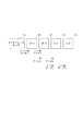
また、実施形態1では、画像処理チップ、エンジンチップを2個ずつ使用した画像形成システムを示したが、これに限定されるものではない。図8は、画像処理チップ及びエンジンチップ共に4個ずつで構成した例、すなわち、図6に示したチップ構成と比較して画像処理チップ及びエンジンチップが共に倍としたものである。図8を用いて、12色を扱うことが可能なプリンタで、各チップに3色ずつを割り当てて構成する例について説明する。図8において、画像処理チップIP−A109、画像処理チップIP−B111、画像処理チップIP−C701、画像処理チップIP−D702は、図7で説明した画像処理チップと同様に各々4色の画像データを並列処理可能な回路ブロックを搭載している。また、エンジンチップE−A113、エンジンチップE−B115、エンジンチップE−C703、エンジンチップE−D704は、それぞれ、図7で説明したエンジンチップと同様に各々4色の画像データを並列処理可能な回路ブロックを搭載している。
In the first embodiment, an image forming system using two image processing chips and two engine chips is shown. However, the present invention is not limited to this. FIG. 8 shows an example in which four image processing chips and four engine chips are provided, that is, both the image processing chip and the engine chip are doubled as compared with the chip configuration shown in FIG. An example in which a printer capable of handling 12 colors is configured by assigning 3 colors to each chip will be described with reference to FIG. In FIG. 8, an image processing chip IP-
データ1は、実施形態1と同様に、RGBデータである。データ1は、これを画像処理に使用する画像処理チップIP−A109、IP−B111、IP−C701、IP−D702へ転送される。
まず、データ1は、IP−A109で処理されて二値画像データ3色(例えばC、M、Y)のデータ4となる。生成されたデータ4は、データ4を使用するエンジンチップE−A113へ到達するまで、チップ間を転送される。すなわち、IP−B111、IP−C701、IP−D702を経由して、エンジンチップE−A113へ到達する。
First,
また、データ1は、IP−B111で処理されて二値画像データ3色(例えば、ライトシアンLC、ライトマゼンタLM、ブラックBK)のデータ5となる。生成されたデータ5は、データ5を使用するエンジンチップE−B115へ到達するまで、チップ間を転送される。すなわち、IP−C701、IP−D702、E−A113を経由して、エンジンチップE−B115へ到達する。
データ1は、IP−C701で処理されて二値画像データ3色(上記以外のインク3色)のデータ6となり、また、IP−D702で処理されて二値画像データ3色(さらに残ったインク3色)のデータ7となる。データ6及びデータ7は、インク色データを使用するチップ、それぞれE−C703及びE−D704まで同様に転送される。
実施形態1及び図8を用いて説明した通り、最大4色を同時処理可能な同一のチップを用いながら画像処理システムを構成するチップの個数を変更することで、4色プリンタにも、12色プリンタにも対応することが可能となる。すなわち、チップの個数を適宜変更することにより、画像処理システムの画像処理装置(本実施形態ではプリンタ)で使用するインク色に対応することができる。また、上述した通り、各チップに対して異なる色を割り当てて処理するため、各チップで行う画像処理、データ転送処理は同じアルゴリズムのプログラムを使用することができる。すなわち、同一構成からなるチップを色数だけを変更して使用することが可能となる。したがって、複雑な処理を行うことなく、処理の高速化を実現することができる。また、上述した実施形態では、チップ間を接続する際にPCIeを用いたが、チップ間を接続するインタフェースであれば、これに限定されるものではない。 As described with reference to the first embodiment and FIG. 8, by using the same chip capable of simultaneously processing a maximum of four colors, the number of chips constituting the image processing system is changed, so that a four-color printer also has 12 colors. It is also possible to support a printer. In other words, by appropriately changing the number of chips, it is possible to cope with the ink color used in the image processing apparatus (printer in this embodiment) of the image processing system. Further, as described above, since different colors are assigned to each chip for processing, the same algorithm program can be used for image processing and data transfer processing performed on each chip. That is, it is possible to use chips having the same configuration by changing only the number of colors. Therefore, it is possible to realize high-speed processing without performing complicated processing. In the above-described embodiment, PCIe is used when connecting chips. However, the embodiment is not limited to this as long as it is an interface that connects chips.
実施形態1では、チップ間のデータ転送を行う際、あらかじめ設定されたチップ内のアドレスに対して転送することで、次段のチップへデータをそのまま転送するバッファと自身の画像処理に使用するデータのバッファに分けて受信動作可能な機構を示した。しかしながら、チップ間のデータ転送方式は、チップ間のデータ転送をすることができるものであれば、これに限定されるものではない。実施形態1では、前段のチップから受信したデータを一旦RAM上に格納するものとしたが、これに限定されるものではない。例えば、前段のチップから受信したデータはRAM上に格納せず、チップ内のクロスバースイッチで直接次段チップのIO領域アドレスへルーティングしてチップ内をスルーさせても良い。すなわち、図3においてPCIeコントローラA300を通じて受信したデータをクロスバースイッチ301経由でPCIeコントローラB308へ出力するデータパスとしてもよい。このような方式を用いても実施形態1と同様の効果を奏する。また、他の方式として、例えばデータをパケット単位で転送し、パケットにどのチップで使用するデータかを示す情報を付加しても良い。すなわち、受信したチップでパケット内の情報を解析して自身で使用するか、次段のチップへ転送するかを判断する方式を用いても実施形態1と同様の効果を奏する。
In the first embodiment, when transferring data between chips, by transferring to a preset address within the chip, a buffer for transferring data as it is to the next chip and data used for its own image processing A mechanism that can receive data by dividing it into multiple buffers is shown. However, the data transfer method between chips is not limited to this as long as data transfer between chips is possible. In the first embodiment, the data received from the preceding chip is temporarily stored in the RAM. However, the present invention is not limited to this. For example, the data received from the previous chip may not be stored in the RAM, but may be routed directly to the IO area address of the next chip by a crossbar switch in the chip and passed through the chip. That is, in FIG. 3, the data path may be a data path for outputting data received through the
また、画像処理チップとエンジンチップを接続する順序は、実施形態1や図8で説明した例に限定されるものではない。すなわち、画像処理チップをすべて接続した後に、エンジンチップをすべて接続するものに限定されるものではない。例えば、図9に示すように、画像処理チップ、エンジンチップを各2チップ使用する場合、画像チップとエンジンチップを交互に接続してもよい。画像処理チップ、エンジンチップを各4チップ使用する場合も同様に、図10に示すように、画像処理チップとエンジンチップを交互に接続してもよい。この接続構成の場合、インタフェースチップ104で生成されたデータ1は、画像処理チップのそれぞれに転送される。このとき、図9及び図10に示すように、チップ間を転送する。また、画像処理チップで生成されたデータ(データ2、データ3、データ4、データ5)は、それぞれ対応するエンジンチップに送信するために、チップ間を転送される。図9の構成において、各チップに割り当てる色数を実施形態1と同様に2色とすれば、4色プリンタに対応することが可能となる。また、図10の構成において、各チップに割り当てる色数を3色とした場合、12色プリンタに対応することが可能となる。
Further, the order of connecting the image processing chip and the engine chip is not limited to the example described in the first embodiment and FIG. That is, the invention is not limited to connecting all the engine chips after connecting all the image processing chips. For example, as shown in FIG. 9, when two image processing chips and two engine chips are used, the image chip and the engine chip may be alternately connected. Similarly, when using four image processing chips and four engine chips, as shown in FIG. 10, the image processing chips and the engine chips may be alternately connected. In the case of this connection configuration,
上述した実施形態では、画像処理チップ毎に所定のインク色の画像処理を割り当てる例を示したが、これに限定されるものではない。例えば、異なる画像処理チップに同じインク色の異なるバンドデータの画像処理を割り付ける処理を組み合わせて使用してもよいし、例えば、オブジェクト種毎、画像や文字等の属性毎に画像処理を割り付ける処理を組み合わせてもよい。 In the embodiment described above, an example in which image processing of a predetermined ink color is assigned to each image processing chip has been described, but the present invention is not limited to this. For example, processing for assigning image processing of different band data of the same ink color to different image processing chips may be used in combination. For example, processing for assigning image processing for each object type or for each attribute such as an image or a character. You may combine.
また、画像処理チップ数とエンジンチップ数を同数としたが、これに限定されるものではなく、異なる数となっていてもよい。ただし、画像処理チップ数とエンジンチップスを同数とすることにより、処理を簡略化することができ、また、処理量の多いチップがボトルネックとなるのを防ぐことができる。 Further, although the number of image processing chips and the number of engine chips are the same, the present invention is not limited to this and may be different. However, by making the number of image processing chips equal to the number of engine chips, the processing can be simplified, and chips with a large amount of processing can be prevented from becoming a bottleneck.
さらに、実施形態1では、入力画像データを二値化処理する画像処理チップと二値画像データを処理するエンジンチップが異なるチップに実装されている例を示したが、この構成に限定されるものではない。画像処理チップとエンジンチップに実装されている機能を一つのチップに集積した構成としてもよい。この場合、例えば、一つのチップで処理するインク色の数を少なくすることにより、実施形態1と同様の効果を奏する。 Furthermore, in the first embodiment, the example in which the image processing chip for binarizing input image data and the engine chip for processing binary image data are mounted on different chips has been described. However, the present invention is limited to this configuration. is not. The functions mounted on the image processing chip and the engine chip may be integrated on one chip. In this case, for example, by reducing the number of ink colors processed by one chip, the same effects as those of the first embodiment can be obtained.
また、実施形態1では、チップを基本ユニットとして、チップの個数を増加させることでスケーラブルな処理性能向上を実現する例を示したが、基本ユニットはチップに限定されるものではない。他の例としては、画像処理チップとエンジンチップとそれぞれに接続されるRAMとコネクタをプリント基板に搭載したモジュールをユニットとしたものが挙げられる。コネクタ同士を勘合させた時にモジュール同士が電気的に接続されるようにプリント基板上でパターン配線しておき、このモジュールを複数個縦列に接続することによって、電気的、論理的に各チップを複数個縦列に接続する。このようにユニットをプリント基板モジュールで構成した場合であっても同様の効果を奏する。 In the first embodiment, an example has been shown in which the processing performance is improved by increasing the number of chips using the chip as a basic unit. However, the basic unit is not limited to the chip. As another example, there is a unit in which a module in which a RAM and a connector connected to an image processing chip and an engine chip are mounted on a printed board is united. Pattern wiring is performed on the printed circuit board so that the modules are electrically connected to each other when the connectors are fitted together, and a plurality of modules are electrically and logically connected to each other in multiple columns. Connect to individual columns. Thus, even when the unit is configured by a printed circuit board module, the same effect is obtained.
また、上述した実施形態では、画像処理に用いる画像処理チップ及びエンジンチップについて説明したが、これに限定されるものではない。これらのチップの構成は、複数の処理(実施形態1では、複数のインク色の処理)を実行する場合に有効である。また、各チップは、データの処理機能、転送・出力機能を備えるものであればよい。 In the above-described embodiment, the image processing chip and the engine chip used for image processing have been described. However, the present invention is not limited to this. These chip configurations are effective when executing a plurality of processes (in the first embodiment, a plurality of ink color processes). Each chip only needs to have a data processing function and a transfer / output function.
上述した実施形態では、画像処理装置としてプリンタ101を例示したが、上述した構成を全て含んでいる必要はない。また、画像処理装置の記録方式は、特に限定されず、インクジェット方式であっても、電子写真方式であってもよい。また、画像処理装置は、プリンタに限定されるものではなく、画像処理を行う装置であればよい。
In the above-described embodiment, the
さらに、以上の実施形態の全てをハードウェアで実行する必要はなく、一部をソフトウェアによって構成してもよい。 Furthermore, it is not necessary to execute all of the above embodiments by hardware, and a part may be configured by software.
100 ホストPC
101 プリンタ
102 プリンタコントローラ
103 プリンタエンジン
104 インタフェースチップ
105 ROM
106 RAM
107 操作パネル
108 HDD
109 画像処理チップIP−A
110 RAM
111 画像処理チップIP−B
112 RAM
113 エンジンチップE−A
114 RAM
115 エンジンチップE−B
116 RAM
117 キャリッジ
118 プリントヘッドA
119 プリントヘッドB
120 エンジン制御部
100 host PC
101
106 RAM
107
109 Image processing chip IP-A
110 RAM
111 Image processing chip IP-B
112 RAM
113 Engine chip EA
114 RAM
115 Engine chip EB
116 RAM
117
119 Print head B
120 Engine control unit
Claims (17)
前記第1の画像処理チップと前記第2の画像処理チップとは、直列に接続されており、
前記第1の画像処理チップと前記第2の画像処理チップのそれぞれは、転送手段と画像処理手段とを備え、
前記第1の画像処理チップの前記画像処理手段は、入力された第1の画像データに所定の画像処理を実行して第2の画像データを生成し、前記第1の画像処理チップの前記転送手段は、入力された第1の画像データを画像処理せずに転送し且つ前記第2の画像データを転送し、
前記第1の画像処理チップ及び前記第2の画像処理チップの各画像処理手段は、画像データから量子化データを生成する第1画像処理部と、量子化データから印刷データを生成する第2画像処理部と、のうち少なくともいずれかを備え、
前記第1画像処理部により生成された量子化データは、次の画像処理チップへ転送され、前記第2画像処理部により生成された印刷データは、印刷手段へ転送されることを特徴とする画像処理装置。 A first image processing chip and a second image processing chip for performing image processing on the input image data;
The first image processing chip and the second image processing chip are connected in series,
Each of the first image processing chip and the second image processing chip includes a transfer unit and an image processing unit,
The image processing means of the first image processing chip performs predetermined image processing on the input first image data to generate second image data, and the transfer of the first image processing chip The means transfers the input first image data without image processing and transfers the second image data,
Each image processing means of the first image processing chip and the second image processing chip includes a first image processing unit that generates quantized data from the image data, and a second image that generates print data from the quantized data. And at least one of a processing unit,
The quantized data generated by the first image processing unit is transferred to a next image processing chip, and the print data generated by the second image processing unit is transferred to a printing unit. Processing equipment.
前記第1の画像処理チップと前記第2の画像処理チップとは、直列に接続されており、
前記第1の画像処理チップと前記第2の画像処理チップのそれぞれは、転送手段と画像処理手段とを備え、
前記第1の画像処理チップの前記画像処理手段は、入力された第1の画像データに所定の画像処理を実行して第2の画像データを生成し、前記第1の画像処理チップの前記転送手段は、入力された第1の画像データを画像処理せずに転送し且つ前記第2の画像データを転送し、
前記第1の画像処理チップ及び前記第2の画像処理チップの各画像処理手段は、画像データから量子化データを生成する第1画像処理部と、量子化データから印刷データを生成する第2画像処理部と、のうち少なくともいずれかを備え、
前記第1画像処理部により生成された量子化データは、前記第2画像処理部へ転送され、前記第2画像処理部により生成された印刷データは、印刷手段へ転送されることを特徴とする画像処理装置。 A first image processing chip and a second image processing chip for performing image processing on the input image data;
The first image processing chip and the second image processing chip are connected in series,
Each of the first image processing chip and the second image processing chip includes a transfer unit and an image processing unit,
The image processing means of the first image processing chip performs predetermined image processing on the input first image data to generate second image data, and the transfer of the first image processing chip The means transfers the input first image data without image processing and transfers the second image data,
Each image processing means of the first image processing chip and the second image processing chip includes a first image processing unit that generates quantized data from the image data, and a second image that generates print data from the quantized data. And at least one of a processing unit,
The quantized data generated by the first image processing unit is transferred to the second image processing unit, and the print data generated by the second image processing unit is transferred to a printing unit. Image processing device.
前記第2の画像データは、インク色空間のデータであることを特徴とする請求項1〜12のいずれか1項に記載の画像処理装置。 The first image data is RGB color space data,
The image processing apparatus according to claim 1, wherein the second image data is ink color space data.
前記第1の画像処理チップと前記第2の画像処理チップとは、直列に接続されており、
前記第1の画像処理チップと前記第2の画像処理チップのそれぞれにおいて、画像処理工程と転送工程が実行され、
前記第1の画像処理チップにおいて、入力された第1の画像データに所定の画像処理を実行して第2の画像データを生成する画像処理工程と、入力された第1の画像データを画像処理せずに転送し且つ前記第2の画像データを転送する転送工程と、が実行され、
前記第1の画像処理チップ及び前記第2の画像処理チップの各画像処理工程は、画像データから量子化データを生成する第1画像処理工程と、量子化データから印刷データを生成する第2画像処理工程と、のうち少なくともいずれかを備え、
前記第1画像処理工程により生成された量子化データは、次の画像処理チップへ転送され、前記第2画像処理工程により生成された印刷データは、印刷手段へ転送されることを特徴とする画像処理方法。 In an image processing method using a first image processing chip and a second image processing chip for executing image processing on input image data,
The first image processing chip and the second image processing chip are connected in series,
In each of the first image processing chip and the second image processing chip, an image processing step and a transfer step are executed,
In the first image processing chip, an image processing step of generating predetermined image processing on the input first image data to generate second image data, and image processing on the input first image data Transferring without transferring and transferring the second image data,
Each image processing step of the first image processing chip and the second image processing chip includes a first image processing step for generating quantized data from image data, and a second image for generating print data from the quantized data. And at least one of processing steps,
The quantized data generated by the first image processing step is transferred to the next image processing chip, and the print data generated by the second image processing step is transferred to a printing unit. Processing method.
前記第1の画像処理チップと前記第2の画像処理チップとは、直列に接続されており、
前記第1の画像処理チップと前記第2の画像処理チップのそれぞれにおいて、画像処理工程と転送工程が実行され、
前記第1の画像処理チップにおいて、入力された第1の画像データに所定の画像処理を実行して第2の画像データを生成する画像処理工程と、入力された第1の画像データを画像処理せずに転送し且つ前記第2の画像データを転送する転送工程と、が実行され、
前記第1の画像処理チップ及び前記第2の画像処理チップの各画像処理工程は、画像データから量子化データを生成する第1画像処理工程と、量子化データから印刷データを生成する第2画像処理工程と、のうち少なくともいずれかを備え、
前記第1画像処理工程により生成された量子化データは、前記第2画像処理工程へ転送され、前記第2画像処理工程により生成された印刷データは、印刷手段へ転送されることを特徴とする画像処理方法。 In an image processing method using a first image processing chip and a second image processing chip for executing image processing on input image data,
The first image processing chip and the second image processing chip are connected in series,
In each of the first image processing chip and the second image processing chip, an image processing step and a transfer step are executed,
In the first image processing chip, an image processing step of generating predetermined image processing on the input first image data to generate second image data, and image processing on the input first image data Transferring without transferring and transferring the second image data,
Each image processing step of the first image processing chip and the second image processing chip includes a first image processing step for generating quantized data from image data, and a second image for generating print data from the quantized data. And at least one of processing steps,
The quantized data generated by the first image processing step is transferred to the second image processing step, and the print data generated by the second image processing step is transferred to a printing unit. Image processing method.
Priority Applications (3)
| Application Number | Priority Date | Filing Date | Title |
|---|---|---|---|
| JP2013088705A JP6230258B2 (en) | 2013-04-19 | 2013-04-19 | Image processing apparatus and image processing method |
| US14/254,672 US9361057B2 (en) | 2013-04-19 | 2014-04-16 | Image processing apparatus and image processing method for executing image processing using multiple image processing units |
| US15/145,166 US9953251B2 (en) | 2013-04-19 | 2016-05-03 | Image processing apparatus and image processing method for executing image processing using multiple serial image processing units to process different colors |
Applications Claiming Priority (1)
| Application Number | Priority Date | Filing Date | Title |
|---|---|---|---|
| JP2013088705A JP6230258B2 (en) | 2013-04-19 | 2013-04-19 | Image processing apparatus and image processing method |
Publications (3)
| Publication Number | Publication Date |
|---|---|
| JP2014211815A JP2014211815A (en) | 2014-11-13 |
| JP2014211815A5 JP2014211815A5 (en) | 2016-06-16 |
| JP6230258B2 true JP6230258B2 (en) | 2017-11-15 |
Family
ID=51728781
Family Applications (1)
| Application Number | Title | Priority Date | Filing Date |
|---|---|---|---|
| JP2013088705A Active JP6230258B2 (en) | 2013-04-19 | 2013-04-19 | Image processing apparatus and image processing method |
Country Status (2)
| Country | Link |
|---|---|
| US (2) | US9361057B2 (en) |
| JP (1) | JP6230258B2 (en) |
Cited By (1)
| Publication number | Priority date | Publication date | Assignee | Title |
|---|---|---|---|---|
| US11044370B2 (en) | 2018-05-17 | 2021-06-22 | Canon Kabushiki Kaisha | Image processing apparatus and image processing method |
Families Citing this family (1)
| Publication number | Priority date | Publication date | Assignee | Title |
|---|---|---|---|---|
| JP6606389B2 (en) | 2015-09-29 | 2019-11-13 | キヤノン株式会社 | Recording control apparatus, recording apparatus, and data processing method |
Family Cites Families (16)
| Publication number | Priority date | Publication date | Assignee | Title |
|---|---|---|---|---|
| JPH0765145A (en) * | 1993-08-24 | 1995-03-10 | Canon Inc | Image processor and image processing system |
| JP4155472B2 (en) * | 1996-08-28 | 2008-09-24 | セイコーエプソン株式会社 | Recording method and recording apparatus |
| US6081344A (en) * | 1997-10-30 | 2000-06-27 | Hewlett-Packard Company | Device state error diffusion technique for halftoning |
| US7269785B1 (en) * | 1999-12-30 | 2007-09-11 | Genesis Microchip Inc. | Digital manipulation of video in digital video player |
| JP3504210B2 (en) * | 2000-03-31 | 2004-03-08 | 理想科学工業株式会社 | Image processing device |
| AU2003901297A0 (en) * | 2003-03-20 | 2003-04-03 | Silverbrook Research Pty Ltd | Systems and apparatus (fpd001) |
| JP2005094126A (en) * | 2003-09-12 | 2005-04-07 | Canon Inc | Image processing apparatus, image processing method, and image processing program executable by computer |
| US7058738B2 (en) * | 2004-04-28 | 2006-06-06 | Microsoft Corporation | Configurable PCI express switch which allows multiple CPUs to be connected to multiple I/O devices |
| JP4287325B2 (en) | 2004-05-10 | 2009-07-01 | 株式会社リコー | Imaging system |
| US20050248584A1 (en) * | 2004-05-10 | 2005-11-10 | Koji Takeo | Imaging system and image processing apparatus |
| EP1722547A3 (en) * | 2005-04-11 | 2008-10-01 | Ricoh Company, Ltd. | Image processing apparatus and image forming apparatus |
| JP4696804B2 (en) * | 2005-09-16 | 2011-06-08 | セイコーエプソン株式会社 | Image output device |
| JP2008131498A (en) * | 2006-11-22 | 2008-06-05 | Matsushita Electric Ind Co Ltd | Video processor |
| JP2008288795A (en) * | 2007-05-16 | 2008-11-27 | Canon Inc | Image output device |
| JP5591022B2 (en) * | 2010-08-16 | 2014-09-17 | オリンパス株式会社 | Bus bandwidth monitoring device and bus bandwidth monitoring method |
| JP4952859B1 (en) * | 2011-09-15 | 2012-06-13 | 富士ゼロックス株式会社 | Print data processing system |
-
2013
- 2013-04-19 JP JP2013088705A patent/JP6230258B2/en active Active
-
2014
- 2014-04-16 US US14/254,672 patent/US9361057B2/en active Active
-
2016
- 2016-05-03 US US15/145,166 patent/US9953251B2/en active Active
Cited By (1)
| Publication number | Priority date | Publication date | Assignee | Title |
|---|---|---|---|---|
| US11044370B2 (en) | 2018-05-17 | 2021-06-22 | Canon Kabushiki Kaisha | Image processing apparatus and image processing method |
Also Published As
| Publication number | Publication date |
|---|---|
| US9953251B2 (en) | 2018-04-24 |
| US20160247052A1 (en) | 2016-08-25 |
| US9361057B2 (en) | 2016-06-07 |
| US20140313546A1 (en) | 2014-10-23 |
| JP2014211815A (en) | 2014-11-13 |
Similar Documents
| Publication | Publication Date | Title |
|---|---|---|
| JP3936016B2 (en) | How to print document images | |
| US9208415B2 (en) | Image processing apparatus and method encoding multi-valued image generated with fewer values | |
| US20130070262A1 (en) | Printing device and method of controlling printing device | |
| JP6230258B2 (en) | Image processing apparatus and image processing method | |
| JPH11252366A (en) | Printer controller, printer and printing system | |
| JP2001325087A (en) | Command analysis utilizing rewritable command storing part | |
| US10635955B1 (en) | Image forming method, apparatus, and program separating addresses for storing color tone data by shifting the relative address using an offset address | |
| US9467709B2 (en) | Data decoding device and process operating depending on selected modes | |
| JP5082686B2 (en) | Print head control device | |
| JP6559033B2 (en) | Recording control apparatus, recording apparatus, and data processing method | |
| US11442870B2 (en) | Information processing apparatus having an integrated circuit chip with first and second communication units having address translation function | |
| US9019521B2 (en) | DMA transfer of data | |
| JP4345055B2 (en) | Image processing apparatus and method, and printer system | |
| JP5057548B2 (en) | Image data transfer apparatus and image data transfer method | |
| US11521302B2 (en) | Image processing apparatus and image processing method | |
| JP3427975B2 (en) | Printer control circuit, printer and print system | |
| JP2000047976A (en) | Printer control unit | |
| JP4631509B2 (en) | Liquid ejector | |
| JP4492362B2 (en) | Image forming apparatus capable of improving image quality | |
| JPH11179975A (en) | Color printer control device | |
| JP2001047677A (en) | Printer control apparatus | |
| JP2007069424A (en) | Printer | |
| JP2006192618A (en) | Image forming apparatus with printing starting time shortened | |
| KR20060054727A (en) | Apparatus for generating color image | |
| JP2002240261A (en) | Print buffer memory controller |
Legal Events
| Date | Code | Title | Description |
|---|---|---|---|
| A521 | Request for written amendment filed |
Free format text: JAPANESE INTERMEDIATE CODE: A523 Effective date: 20160419 |
|
| A621 | Written request for application examination |
Free format text: JAPANESE INTERMEDIATE CODE: A621 Effective date: 20160419 |
|
| A977 | Report on retrieval |
Free format text: JAPANESE INTERMEDIATE CODE: A971007 Effective date: 20170330 |
|
| A131 | Notification of reasons for refusal |
Free format text: JAPANESE INTERMEDIATE CODE: A131 Effective date: 20170404 |
|
| A521 | Request for written amendment filed |
Free format text: JAPANESE INTERMEDIATE CODE: A523 Effective date: 20170602 |
|
| A131 | Notification of reasons for refusal |
Free format text: JAPANESE INTERMEDIATE CODE: A131 Effective date: 20170704 |
|
| A521 | Request for written amendment filed |
Free format text: JAPANESE INTERMEDIATE CODE: A523 Effective date: 20170901 |
|
| TRDD | Decision of grant or rejection written | ||
| A01 | Written decision to grant a patent or to grant a registration (utility model) |
Free format text: JAPANESE INTERMEDIATE CODE: A01 Effective date: 20170919 |
|
| A61 | First payment of annual fees (during grant procedure) |
Free format text: JAPANESE INTERMEDIATE CODE: A61 Effective date: 20171017 |
|
| R151 | Written notification of patent or utility model registration |
Ref document number: 6230258 Country of ref document: JP Free format text: JAPANESE INTERMEDIATE CODE: R151 |