JP6202575B2 - Mask for array - Google Patents

Mask for array Download PDF

Info

Publication number
JP6202575B2
JP6202575B2 JP2014112483A JP2014112483A JP6202575B2 JP 6202575 B2 JP6202575 B2 JP 6202575B2 JP 2014112483 A JP2014112483 A JP 2014112483A JP 2014112483 A JP2014112483 A JP 2014112483A JP 6202575 B2 JP6202575 B2 JP 6202575B2
Authority
JP
Japan
Prior art keywords
mask
pattern
workpiece
protrusion
holes
Prior art date
Legal status (The legal status is an assumption and is not a legal conclusion. Google has not performed a legal analysis and makes no representation as to the accuracy of the status listed.)
Active
Application number
JP2014112483A
Other languages
Japanese (ja)
Other versions
JP2014197694A (en
Inventor
良弘 小林
良弘 小林
裕仁 田丸
裕仁 田丸
樹一郎 石川
樹一郎 石川
貴士 中島
貴士 中島
Current Assignee (The listed assignees may be inaccurate. Google has not performed a legal analysis and makes no representation or warranty as to the accuracy of the list.)
Hitachi Maxell Energy Ltd
Original Assignee
Hitachi Maxell Energy Ltd
Priority date (The priority date is an assumption and is not a legal conclusion. Google has not performed a legal analysis and makes no representation as to the accuracy of the date listed.)
Filing date
Publication date
Application filed by Hitachi Maxell Energy Ltd filed Critical Hitachi Maxell Energy Ltd
Priority to JP2014112483A priority Critical patent/JP6202575B2/en
Publication of JP2014197694A publication Critical patent/JP2014197694A/en
Application granted granted Critical
Publication of JP6202575B2 publication Critical patent/JP6202575B2/en
Active legal-status Critical Current
Anticipated expiration legal-status Critical

Links

Images

Landscapes

  • Electric Connection Of Electric Components To Printed Circuits (AREA)

Description

本発明は、半田バンプを形成するために使用される配列用マスクに関する。   The present invention relates to an alignment mask used for forming solder bumps.

半田バンプの形成方法としては、半田ボールをワーク上に搭載する方法が知られている。これは、ワークの電極の配列パターンに対応し、半田ボールが挿通可能な通孔からなるパターン領域を有する配列用マスクを用いて半田ボールを搭載する方法である。係る配列用マスクとしては、特許文献1及び2が開示されている。   As a method for forming solder bumps, a method of mounting solder balls on a workpiece is known. This is a method of mounting a solder ball using an array mask having a pattern region that includes a through-hole through which a solder ball can be inserted, corresponding to the array pattern of workpiece electrodes. Patent Documents 1 and 2 are disclosed as such an array mask.

特開2006−287215号公報JP 2006-287215 A 特開2006−324618号公報JP 2006-324618 A

係る配列用マスクは、ワーク内もしくはワークの下方に配置された磁石の磁力を作用させることでワーク上に固定(位置合わせ)される。しかしながら、この配列用マスクのパターン領域には通孔が形成されているものの、パターン領域の外周においては、通孔はなく平板状であるので、配列用マスクをワーク上に載置した際、このパターン領域の外周にて磁力が強く作用されてしまい、配列用マスクにうねりが生じていた。このため、パターン領域のパターンピッチにズレが生じ、半田ボールの搭載不良を招き、生産性が悪かった。   Such an array mask is fixed (positioned) on the workpiece by applying the magnetic force of a magnet arranged in the workpiece or below the workpiece. However, although through holes are formed in the pattern area of this array mask, there are no through holes in the outer periphery of the pattern area and it is flat, so when the array mask is placed on the workpiece, The magnetic force is strongly applied on the outer periphery of the pattern region, and the array mask is swelled. For this reason, the pattern pitch of the pattern region is shifted, causing mounting failure of the solder balls, and the productivity is poor.

本発明の目的は、上述した課題を解決することができる配列用マスクを提供することにある。   The objective of this invention is providing the mask for arrangement | sequence which can solve the subject mentioned above.

本発明は、所定の配列パターンに対応した通孔12内に半田ボール2を振り込むことで、ワーク3上の所定位置に半田ボール2を搭載する配列用マスクであって、通孔12からなるパターン領域が多数形成されたマスク本体10と、マスク本体10のワーク3との対向面側に設けられた突起部15とを備え、突起部15がパターン領域間に形成されており、パターン領域間にピッチ調整部50を構成する凹部52または蛇腹状部53を設け磁力の作用を弱めることを特徴とする。


The present invention is an array mask in which the solder balls 2 are mounted at predetermined positions on the work 3 by swinging the solder balls 2 into the through holes 12 corresponding to the predetermined array pattern. A mask body 10 in which a large number of regions are formed and a projection 15 provided on the surface of the mask body 10 facing the workpiece 3 are provided between the pattern regions. characterized in that weaken the magnetic force provided a concave portion 52 or the bellows-like portion 53 that make up the pitch adjustment section 50.


また、突起部15がパターン領域を囲むようにパターン領域ごとに形成されており、ピッチ調整部50は、パターン領域間、且つ突起部15間に設けられていることを特徴とする。

Further, butt raised portion 15 is formed in each pattern region so as to surround a pattern region, pitch adjustment unit 50 is characterized in that provided between the pattern region, and between the projection 15.

さらに、通孔12や突起部15の形状がテーパ状であることを特徴とする。   Furthermore, the shape of the through-hole 12 and the protrusion 15 is tapered.

本発明に係る配列用マスクによれば、マスク本体とワークとの対向間隙を確保する突起部がパターン領域間に形成されていることにより、パターン領域に対する磁力の影響を抑えることができ、配列用マスクのうねりの発生を防ぐことができるので、パターン領域のパターンピッチズレを防ぐことができる。したがって、半田ボールの搭載不良を防止することができる。また、パターン領域間にピッチ調整部が設けられていることにより、パターン領域の外周における磁力作用を弱めることができ、配列用マスクのうねりの発生をより防ぐことができる。さらに、ピッチ調整部がパターン領域間、且つ突起部間に設けられていることにより、パターン領域へのうねりの影響を可及的に抑えることができる。   According to the arrangement mask according to the present invention, the projections that secure the gap between the mask main body and the workpiece are formed between the pattern areas, so that the influence of the magnetic force on the pattern area can be suppressed, Since the generation of the undulation of the mask can be prevented, the pattern pitch deviation in the pattern area can be prevented. Therefore, mounting failure of solder balls can be prevented. In addition, since the pitch adjusting portion is provided between the pattern regions, the magnetic force action on the outer periphery of the pattern region can be weakened, and the occurrence of the undulation of the array mask can be further prevented. Furthermore, since the pitch adjusting portion is provided between the pattern regions and between the protrusions, the influence of the undulation on the pattern region can be suppressed as much as possible.

本発明に係る配列用マスクとワークの全体構成を示す斜視図である。It is a perspective view which shows the whole structure of the mask for arrangement | sequence which concerns on this invention, and a workpiece | work. 本発明に係る配列用マスクを模式的に示す縦断側面図である。It is a vertical side view which shows typically the mask for arrangement | sequence which concerns on this invention. 本発明に係る別の配列用マスクを模式的に示す縦断側面図である。It is a vertical side view which shows typically the mask for another arrangement | sequence which concerns on this invention. 本発明に係る配列用マスクとワークとの位置関係を示す平面図である。It is a top view which shows the positional relationship of the mask for arrangement | sequence which concerns on this invention, and a workpiece | work. 本発明に係る配列用マスクの製造方法の説明図である。It is explanatory drawing of the manufacturing method of the mask for arrangement | sequence which concerns on this invention. 本発明に係る配列用マスクの製造方法の説明図である。It is explanatory drawing of the manufacturing method of the mask for arrangement | sequence which concerns on this invention. 本発明に係る更に別の配列用マスクを模式的に示す縦断側面図である。It is a vertical side view showing typically another arrangement mask concerning the present invention. 本発明の第1実施形態に係る配列用マスクの部分縦断側面図である。It is a partial vertical side view of the arrangement | sequence mask which concerns on 1st Embodiment of this invention. 本発明の第1実施形態に係る別の配列用マスクの部分平面図である。It is a partial top view of another mask for arrangement concerning a 1st embodiment of the present invention. 本発明の第1実施形態に係る別の配列用マスクの部分縦断側面図である。It is a partial vertical side view of another arrangement mask according to the first embodiment of the present invention. 本発明の第1実施形態に係る別の配列用マスクの部分縦断側面図である。It is a partial vertical side view of another arrangement mask according to the first embodiment of the present invention. 本発明の第1実施形態に係る別の配列用マスクの部分縦断側面図である。It is a partial vertical side view of another arrangement mask according to the first embodiment of the present invention. 本発明の第2実施形態に係る配列用マスクの説明図である。It is explanatory drawing of the mask for arrangement | sequence which concerns on 2nd Embodiment of this invention. 本発明の第2実施形態に係る別の配列用マスクの部分平面図である。It is a fragmentary top view of another mask for arrangement concerning a 2nd embodiment of the present invention. 本発明に係る別の配列用マスクとワークとの位置関係を示す平面図である。It is a top view which shows the positional relationship of another mask for arrangement | sequence which concerns on this invention, and a workpiece | work. 本発明に係る別の配列用マスクとワークとの位置関係を示す平面図である。It is a top view which shows the positional relationship of another mask for arrangement | sequence which concerns on this invention, and a workpiece | work.

(配列用マスクの概要)
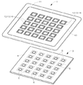
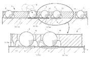
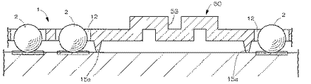
図1乃至図3に、本発明に係る半田ボールの配列用マスクを示す。この配列用マスク(以下、単にマスクと記す)1は、半田バンプ形成における半田ボール2の配列工程において使用に供されるものである。図2における符号3は、マスク1による半田ボール2の搭載対象となるワークを示す。このワーク3にはウエハや基板があるが、例えば、ガラスエポキシ基板のベース4に複数個の半導体チップ5を搭載し、ワイヤボンドで配線した後トランスファモールド封止してなるものであり、半導体チップ5を囲むように、ワーク3の上面には、入出力端子である電極6が所定のパターンで形成されている。なお、ワーク3は、バンプの形成後に個片に切断され、個々のLSIチップとされる。
(Outline of array mask)
1 to 3 show a solder ball arrangement mask according to the present invention. This arrangement mask (hereinafter simply referred to as a mask) 1 is used in the arrangement process of the solder balls 2 in the formation of solder bumps. Reference numeral 3 in FIG. 2 indicates a workpiece on which the solder ball 2 is mounted by the mask 1. The work 3 includes a wafer and a substrate. For example, a plurality of semiconductor chips 5 are mounted on a base 4 of a glass epoxy substrate, wired by wire bonding, and then sealed by transfer molding. 5, electrodes 6 as input / output terminals are formed in a predetermined pattern on the upper surface of the work 3. The work 3 is cut into individual pieces after the bumps are formed to form individual LSI chips.

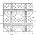
図1に示すように、マスク1は、ニッケルやニッケルコバルト等のニッケル合金、銅やその他の金属を素材として形成されたマスク本体10から成り、このマスク本体10にはこれを囲むように枠体11を装着できる。マスク本体10の盤面中央部には、各半導体チップ5に対応して、半田ボール2を投入するための多数独立の通孔12からなるパターン領域が多数形成されている。通孔12は、図2に示すように、ワーク3上における各半導体チップ5の電極6の配列位置に対応した配列パターンとなっている。半田ボール2は、50μm以下の半径寸法を有するものであり、これに合わせて各通孔12は、当該ボール2の半径寸法よりも僅かに大きな内径寸法を有する平面視で円形状に形成されている。   As shown in FIG. 1, the mask 1 is composed of a mask main body 10 made of a nickel alloy such as nickel or nickel cobalt, copper or other metal as a raw material, and the mask main body 10 surrounds the frame body. 11 can be installed. In the center of the board surface of the mask main body 10, a large number of pattern regions each including a large number of independent through holes 12 for inserting the solder balls 2 are formed corresponding to the respective semiconductor chips 5. As shown in FIG. 2, the through holes 12 have an arrangement pattern corresponding to the arrangement positions of the electrodes 6 of the respective semiconductor chips 5 on the workpiece 3. The solder ball 2 has a radial dimension of 50 μm or less, and in accordance with this, each through hole 12 is formed in a circular shape in plan view having an inner diameter dimension slightly larger than the radial dimension of the ball 2. Yes.

マスク本体10には、補強用の枠体11を装着することができる。この枠体11は、アルミ、42アロイ、インバー材、SUS430等の材質からなる平板体であり、その盤面中央に、マスク本体10に対応する一つの四角形状の開口を備えており、一枚のマスク本体10を一枚の枠体11で保持している。枠体11は、マスク本体10よりも肉厚の成形品であり、マスク本体10の外周縁と不離一体的に接合される。この枠体11の厚み寸法は、例えば、0.05〜1.0mm程度とし、ここでは、0.5mmに設定した。また、マスク本体10の厚みは、10μm以上が好ましく、ここでは、200μmに設定した。   A reinforcing frame 11 can be attached to the mask body 10. This frame 11 is a flat plate made of a material such as aluminum, 42 alloy, Invar, SUS430, etc., and has one rectangular opening corresponding to the mask body 10 at the center of the board surface. The mask body 10 is held by a single frame 11. The frame 11 is a molded product that is thicker than the mask body 10, and is integrally and integrally joined to the outer peripheral edge of the mask body 10. The thickness dimension of the frame 11 is, for example, about 0.05 to 1.0 mm, and is set to 0.5 mm here. The thickness of the mask main body 10 is preferably 10 μm or more, and is set to 200 μm here.

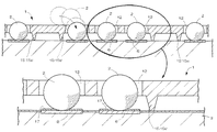
マスク本体10(マスク1)の下面側、すなわちワーク3との対向面側には、下方向に突出状の突起部15を設けることができる。詳しくは、図2及び図4に示すように、パターン領域の外周(パターン領域間)にこのパターン領域を囲むように桟状の突起部15aを設けることができる。また、図3に示すように、パターン領域内の通孔12が形成されていない位置に突起部15bを設けることができる。係る突起部15を設けていれば、配列作業時において、ワーク3の上面に当接してマスク本体10とワーク3との対向間隙を確保できる。各々の突起部15、特に突起部15bにおいては、図2および図3に示すように、通孔12間であって、マスク本体10の下面から先窄まるように形成されていることが好ましく、円錐台状を呈している。また、突起部15の高さとマスク本体10の厚みとの比が2対1以上とするのが好ましく、上記マスク本体10の厚さが10〜300μmの範囲内において、これを満足することがより好ましい。また、突起部15の先端の径L1と付け根の径L2との比が1対3以上であることが好ましい。さらに言えば、突起部15の先端の径と付け根の径と通孔12間の幅との比が1対3対3以上であることが好ましい。また、この突起部15は、アスペクト比(突起部15の高さと先端径との比)が大きいものが好ましく、アスペクト比3としている。なお、図2、図3、図4に示すように、隣り合うパターン領域間にはパターン領域を囲むようにして突起部15aを設けて、マスク1をワーク3に載置した時に当接するようにしているが、図15に示すように、隣り合うパターン領域間全体が突起部15aとした形態であっても良いし、図16に示すように、突起部15aを設けない形態であっても良い。また、図4、図15、図16において、符号15で図示しているのは、突起部15の下端面であり、突起部15の付け根は図示していない。   On the lower surface side of the mask main body 10 (mask 1), that is, the surface facing the workpiece 3, a protruding portion 15 that protrudes downward can be provided. Specifically, as shown in FIGS. 2 and 4, a beam-like protrusion 15 a can be provided on the outer periphery of the pattern area (between the pattern areas) so as to surround the pattern area. Moreover, as shown in FIG. 3, the protrusion part 15b can be provided in the position in which the through-hole 12 in the pattern area | region is not formed. If the projecting portion 15 is provided, it is possible to secure a facing gap between the mask main body 10 and the workpiece 3 by contacting the upper surface of the workpiece 3 during the arraying operation. As shown in FIGS. 2 and 3, each of the protrusions 15, particularly the protrusions 15 b, is preferably formed so as to be tapered from the lower surface of the mask body 10 between the through holes 12. It has a truncated cone shape. Further, the ratio of the height of the protrusion 15 to the thickness of the mask body 10 is preferably 2 to 1 or more, and it is more preferable that the thickness of the mask body 10 is within a range of 10 to 300 μm. preferable. Moreover, it is preferable that the ratio between the diameter L1 of the tip of the protrusion 15 and the diameter L2 of the root is 1: 3 or more. Furthermore, it is preferable that the ratio of the diameter of the tip of the protrusion 15, the diameter of the base, and the width between the through holes 12 is 1 to 3 to 3 or more. The protrusion 15 preferably has a large aspect ratio (ratio between the height of the protrusion 15 and the tip diameter), and has an aspect ratio of 3. As shown in FIGS. 2, 3, and 4, a protrusion 15 a is provided between adjacent pattern areas so as to surround the pattern area so that the mask 1 is brought into contact with the workpiece 3 when it is placed on the work 3. However, as shown in FIG. 15, the form between the adjacent pattern regions may be the protrusions 15 a, or the protrusion 15 a may not be provided as shown in FIG. 16. 4, 15, and 16, the reference numeral 15 indicates the lower end surface of the protrusion 15, and the root of the protrusion 15 is not illustrated.

ここで、図面に記載のマスクは、実際のマスクの様子を示したものではなく、それを模式的に示している。さらに言うと、図1等における通孔12の開口寸法やマスク本体10等の厚み寸法等は、図面作成の便宜上、そのような寸法に示したものである。   Here, the mask described in the drawings does not show the actual state of the mask, but schematically shows it. Further, the opening dimension of the through-hole 12 and the thickness dimension of the mask main body 10 and the like in FIG. 1 and the like are shown in such dimensions for the convenience of drawing.

マスク1を用いた半田ボール2の配列作業は、以下のような手順で行われる。なお、この配列作業は、専用の配列装置(特許文献1の図1、図5等を参照)によって行われる。まず、ワーク3の電極6上にフラックス17(図2参照)を印刷塗布する。次に、通孔12と電極6とが一致するように、ワーク3上にマスク1を位置合わせしたうえで、マスク1を固定する。かかる位置合わせ作業は、実際にはワーク3とマスク本体10の外周縁、もしくはマスク本体10に形成したアライメントマーク(不図示)と位置合わせすることで行われる。位置合わせ作業が終了すると、ワーク3の下方に配置した磁石(不図示)の磁力を作用させ、かかる固定状態において、突起部15の下端面がワーク3の表面に当接することで、マスク本体10は、図2及び図3に示すようなワーク3との対向間隙が確保された離間姿勢に姿勢保持される。ワーク3の表面が僅かにうねっている場合にも、突起部15の下端面をワーク3の表面に当接させて、該ワーク3の表面のうねりに合わせて、マスク本体10を不離一体的に固定することができる。   The operation of arranging the solder balls 2 using the mask 1 is performed in the following procedure. This arrangement work is performed by a dedicated arrangement apparatus (see FIGS. 1 and 5 of Patent Document 1). First, a flux 17 (see FIG. 2) is printed on the electrode 6 of the work 3. Next, after aligning the mask 1 on the work 3 so that the through-hole 12 and the electrode 6 coincide with each other, the mask 1 is fixed. Such alignment work is actually performed by aligning the workpiece 3 with the outer peripheral edge of the mask body 10 or an alignment mark (not shown) formed on the mask body 10. When the alignment operation is completed, the magnetic force of a magnet (not shown) disposed below the work 3 is applied, and the lower end surface of the projection 15 abuts against the surface of the work 3 in such a fixed state. Is held in a separated posture in which a gap facing the workpiece 3 as shown in FIGS. 2 and 3 is secured. Even when the surface of the workpiece 3 is slightly wavy, the mask main body 10 is inseparably integrated so that the lower end surface of the projection 15 is brought into contact with the surface of the workpiece 3 to match the waviness of the surface of the workpiece 3. Can be fixed.

次に、マスク1上に多数個の半田ボール2を供給し、スキージブラシを用いてマスク1上で半田ボール2を分散させて、通孔12内に一つずつ半田ボール2を投入する。これにて、半田ボール2はフラックス17に仮止め状に粘着保持される。かかるスキージブラシを用いた半田ボール2の投入作業において、スキージブラシ圧がマスク1に大きくかかったとしても突起部15によってマスク1が撓むことを防止でき、投入作業を作業効率良くスムーズに進めることができる。   Next, a large number of solder balls 2 are supplied onto the mask 1, the solder balls 2 are dispersed on the mask 1 using a squeegee brush, and the solder balls 2 are put into the through holes 12 one by one. As a result, the solder ball 2 is adhered and held to the flux 17 in a temporarily fixed shape. In the charging operation of the solder ball 2 using such a squeegee brush, even if the squeegee brush pressure is applied to the mask 1, the mask 1 can be prevented from being bent by the projections 15, and the charging operation can be performed smoothly and efficiently. Can do.

係る構成のマスク1によれば、マスク本体10とワーク3との対向間隙を形成する突起部15を備えているので、突起部15によってワーク3との対向間隙を確実に確保でき、通孔12内への半田ボール2の投入作業を効率的に漏れなく進めることが可能となる。   According to the mask 1 having such a configuration, since the projection 15 that forms the opposing gap between the mask main body 10 and the workpiece 3 is provided, the opposing gap with the workpiece 3 can be reliably secured by the projection 15, and the through-hole 12 can be secured. It is possible to efficiently carry out the operation of putting the solder ball 2 into the inside without leakage.

また、マスク本体10の外周縁に、補強用の枠体11を設けることができ、マスク本体10がそれ自体に内方に収縮する方向の応力が作用するようなテンションを加えた状態で形成すれば、周囲温度の変化に伴うマスク本体10の膨張分を、当該収縮方向へのテンションで吸収できる。これにて、ワーク3に対するマスク本体10の位置ズレの発生を防ぐことができる。また、マスク本体10の全体に均一なテンションを与えることができるので、ワーク3に対して半田ボール2を位置精度良く搭載させることができる。   Further, a reinforcing frame 11 can be provided on the outer peripheral edge of the mask body 10, and the mask body 10 is formed in a state where a tension is applied to the mask body 10 so that stress in a direction in which the mask body 10 contracts inwardly acts. For example, the expansion of the mask main body 10 due to the change in the ambient temperature can be absorbed by the tension in the contraction direction. Thereby, it is possible to prevent the positional deviation of the mask main body 10 with respect to the workpiece 3. In addition, since uniform tension can be applied to the entire mask body 10, the solder balls 2 can be mounted on the workpiece 3 with high positional accuracy.

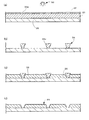
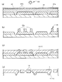
次に、係る構成の配列用マスク1の製造方法を図5及び図6に示す。まず、例えば、導電性を有するステンレス製や真ちゅう鋼製の母型30の表面にフォトレジスト層31を形成する。このフォトレジスト層31は、ネガタイプの感光性ドライフォトレジストを、所定の高さに合わせて一枚ないし数枚ラミネートして熱圧着により形成した。ついで、図5(a)に示すごとく、フォトレジスト層31の上に、突起部15に対応する透光孔32aを有するパターンフィルム(ガラスマスク)32を密着させたのち、紫外光ランプ33で紫外線光を照射して露光を行い、現像、乾燥の各処理を行って、未露光部分を溶解除去することにより、図5(b)に示すように、先窄まり状の突起部15に対応するレジスト体34aを有する一次パターンレジスト34を母型30上に形成した。この時、紫外線が透過しにくいフォトレジストを用いたり、露光量を弱めたりして、レジスト体34aにテーパが付いたものが好ましい。   Next, a method for manufacturing the array mask 1 having such a configuration is shown in FIGS. First, for example, a photoresist layer 31 is formed on the surface of a matrix 30 made of stainless steel or brass having conductivity. The photoresist layer 31 was formed by laminating one or several negative photosensitive dry photoresists to a predetermined height and then thermocompression bonding. Next, as shown in FIG. 5A, a pattern film (glass mask) 32 having a light transmitting hole 32 a corresponding to the protrusion 15 is brought into close contact with the photoresist layer 31, and then an ultraviolet lamp 33 is used for ultraviolet rays. Exposure is performed by irradiating light, development and drying are performed, and unexposed portions are dissolved and removed, thereby corresponding to the tapered protrusions 15 as shown in FIG. A primary pattern resist 34 having a resist body 34 a was formed on the mother die 30. At this time, it is preferable that the resist body 34a has a taper by using a photoresist that does not easily transmit ultraviolet rays or by reducing the exposure amount.

続いて、上記母型30を所定の条件に建浴した電鋳槽に入れ、図5(c)に示すごとく、先のレジスト体34aの高さの範囲内で、母型30のレジスト体34aで覆われていない表面にニッケルや銅等の電着金属を電鋳して、一次電鋳層35を形成した。ここでは、母型30の略全面にわたって、一次電鋳層35を形成した(第一の電鋳工程)。次に、図5(d)に示すごとく、一次パターンレジスト34を除去する。ここで、一次電鋳層35の表面に研磨処理を施しておくと良い。   Subsequently, the mother die 30 is put in an electroforming tank bathed under a predetermined condition, and as shown in FIG. 5C, the resist member 34a of the mother die 30 is within the range of the height of the previous resist member 34a. A primary electroformed layer 35 was formed by electroforming an electrodeposited metal such as nickel or copper on the surface not covered with. Here, the primary electroformed layer 35 was formed over substantially the entire surface of the mother die 30 (first electroforming process). Next, as shown in FIG. 5D, the primary pattern resist 34 is removed. Here, it is preferable to polish the surface of the primary electroformed layer 35.

次いで、図6(a)に示すごとく、一次電鋳層35および母型30の表面の全体に、フォトレジスト層36を形成したうえで、当該フォトレジスト層36の表面に、前記通孔12に対応する透光孔37aを有するパターンフィルム(ガラスマスク)37を密着させたのち、紫外光ランプ33で紫外線光を照射して露光を行い、現像、乾燥の各処理を行って、未露光部分を溶解除去することにより、図6(b)に示すように、マスク本体10に対応するレジスト体38aを有する二次パターンレジスト38を一次電鋳層35の表面に形成した。   Next, as shown in FIG. 6A, a photoresist layer 36 is formed on the entire surface of the primary electroformed layer 35 and the mother die 30, and then the through hole 12 is formed on the surface of the photoresist layer 36. After closely attaching a pattern film (glass mask) 37 having a corresponding light transmitting hole 37a, exposure is performed by irradiating with ultraviolet light with an ultraviolet lamp 33, and development and drying are performed, and an unexposed portion is exposed. By dissolving and removing, a secondary pattern resist 38 having a resist body 38 a corresponding to the mask body 10 was formed on the surface of the primary electroformed layer 35 as shown in FIG.

続いて、所定の条件に建浴した電鋳槽に入れ、図6(c)に示すごとく、先のレジスト体38aの高さの範囲内で、母型30及びのレジスト体38aで覆われていない一次電鋳層35の表面にニッケルや銅等の電着金属を電鋳して、二次電鋳層39を形成した(第二の電鋳工程)。次に、二次パターンレジスト38を溶解除去したうえで、母型30及び一次電鋳層35から二次電鋳層39を剥離することにより、図6(d)および図2に示すようなマスク1を得た。そして、マスク1に枠体11を装着すれば、図1に示すような配列用マスク1が得られる。   Subsequently, it is placed in an electroforming tank bathed under a predetermined condition, and as shown in FIG. 6C, it is covered with the matrix 30 and the resist body 38a within the range of the height of the previous resist body 38a. A secondary electroformed layer 39 was formed by electroforming an electrodeposited metal such as nickel or copper on the surface of the primary electroformed layer 35 that was not present (second electroforming step). Next, the secondary pattern resist 38 is dissolved and removed, and then the secondary electroformed layer 39 is peeled off from the mother die 30 and the primary electroformed layer 35, whereby a mask as shown in FIG. 6 (d) and FIG. 1 was obtained. If the frame 11 is attached to the mask 1, an array mask 1 as shown in FIG. 1 is obtained.

二次電鋳層39、つまりマスク1は、それ自体に内方に収縮する方向の応力が作用するようなテンションを加えた状態で、枠体11に保持することが可能である。かかる応力の付与は、例えば、枠体11とマスク1との熱膨張係数の差を利用して、高温環境下でマスク1の外周縁に枠体11の装着作業を行い、常温時ではマスク1を内方側に収縮させることで実現できる。   The secondary electroformed layer 39, that is, the mask 1, can be held on the frame body 11 in a state where a tension is applied so that a stress in the direction of shrinking inward acts on the secondary electroformed layer 39. The stress is applied by, for example, using the difference in thermal expansion coefficient between the frame 11 and the mask 1 to perform the mounting work of the frame 11 on the outer peripheral edge of the mask 1 in a high temperature environment. This can be realized by contracting the inward side.

以上のようなマスク1の製造方法によれば、電鋳法により高精度に配列用マスクを作製することができるので、半田ボール2を位置精度良くワーク3上に搭載させることができる。突起部15を有するマスク1を一回の電鋳作業(第二の電鋳工程)により不離一体に形成するようにすれば、突起部15を後付けする形態に比べて、該突起部15の破損などの不都合が生じるおそれが少なく、信頼性に優れたマスク1を高精度に得ることができる点でも優れている。また、突起部15をマスク本体10の下面に近づくにつれて大きくなるよう先窄まり状に形成すれば、突起部15の特に付け根(根元)に応力が集中することが回避されるため、突起部15の強度をしっかりと補強できつつ、突起部15をフラックス17が塗布された電極6から離間した状態で電極6間に当接できるので、電極6に塗布されたフラックス17がマスク本体10に付着することによる半田ボール2の搭載不良を防止することができる。この時、突起部15の先端の径と付け根の径との比を1対3以上とすること、突起部15のアスペクト比を3以上とすることでより効果的となる。   According to the manufacturing method of the mask 1 as described above, the arraying mask can be manufactured with high accuracy by the electroforming method, so that the solder balls 2 can be mounted on the workpiece 3 with high positional accuracy. If the mask 1 having the protrusions 15 is formed so as to be inseparably integrated by a single electroforming operation (second electroforming process), the protrusions 15 are damaged as compared with the case where the protrusions 15 are retrofitted. This is also excellent in that the mask 1 having excellent reliability can be obtained with high accuracy. Further, if the protrusion 15 is formed in a tapered shape so as to increase as it approaches the lower surface of the mask body 10, it is possible to avoid stress concentration on the root (base) of the protrusion 15, and thus the protrusion 15. Since the protrusion 15 can be brought into contact with the electrodes 6 in a state of being separated from the electrode 6 to which the flux 17 is applied, the flux 17 applied to the electrode 6 adheres to the mask body 10. Therefore, mounting failure of the solder ball 2 can be prevented. At this time, it becomes more effective by setting the ratio of the diameter of the tip of the protrusion 15 to the diameter of the root to be 1: 3 or more and setting the aspect ratio of the protrusion 15 to be 3 or more.

また、レジストパターンを調整することによって所望のアスペクト比を有する突起部15が容易に得られる。なお、係る構成のマスク1において、通孔12及び突起部15の形状はストレート状としてもテーパ状としても良い。ここで、通孔12や突起部15をテーパ状とする場合について具体的に説明すると、通孔12においては、マスク本体10のワーク3との対向面側に向かって先窄まり状のテーパが設けられていることで、半田ボール2を通孔12内に誘い込みやすくなり、マスク本体10のワーク3との対向面側に向かって先拡がり状のテーパが設けられていることで、マスク本体10のワーク3との対向面側における通孔12周縁にフラックスが付着されることを防止できる。また、突起部15においては、マスク本体10のワーク3との対向面側に向かって先窄まり状のテーパが設けられていることで、ワーク3上へのマスクの載置をしっかりとすることができ、マスク本体10のワーク3との対向面側に向かって先拡がり状のテーパが設けられていることで、ワーク3の電極6が狭ピッチに配列された場合であっても、突起部15の強度を確保しつつ、ワーク3上への突起部15の当接をしっかりと対応することができる。かかる形状は、フォトレジスト層31・36の感光度や露光条件を変更することによって得られる。   Further, the protrusion 15 having a desired aspect ratio can be easily obtained by adjusting the resist pattern. In the mask 1 having such a configuration, the shapes of the through holes 12 and the protrusions 15 may be straight or tapered. Here, the case where the through holes 12 and the protrusions 15 are tapered will be described in detail. In the through holes 12, the tapered shape of the mask body 10 toward the surface facing the workpiece 3 is tapered. By being provided, the solder ball 2 can be easily guided into the through hole 12, and the mask body 10 is provided with a taper that is widened toward the surface of the mask body 10 facing the work 3. It is possible to prevent the flux from adhering to the periphery of the through hole 12 on the side facing the workpiece 3. In addition, the protrusion 15 is provided with a tapered taper toward the surface facing the workpiece 3 of the mask body 10, so that the mask is firmly placed on the workpiece 3. Even if the electrodes 6 of the workpiece 3 are arranged at a narrow pitch by providing a taper that is widened toward the surface facing the workpiece 3 of the mask body 10, the protruding portion The abutment of the projection 15 on the workpiece 3 can be dealt with firmly while ensuring the strength of 15. Such a shape can be obtained by changing the photosensitivity and exposure conditions of the photoresist layers 31 and 36.

また、図7に示すように、突起部15はマスクの下面に近づくにつれて寸法が大きくなる末拡がり形状であって、突起部15の側面(特に付け根部分)を円弧状としても良い。これにより、突起部15の特に根元に応力が集中することにより生じる破損の防止、フラックス17の通孔12への回り込み防止が可能となる。   Further, as shown in FIG. 7, the protruding portion 15 has a diverging shape whose size increases as it approaches the lower surface of the mask, and the side surface (particularly the base portion) of the protruding portion 15 may have an arc shape. As a result, it is possible to prevent breakage caused by stress concentration, particularly at the base of the protrusion 15, and to prevent the flux 17 from entering the through hole 12.

(第1実施形態)
続いて、第1実施形態に係る配列用マスクについて説明する。なお、上記構成と同一の部材には同一の符号を付してその説明を省略する。
(First embodiment)
Next, the arrangement mask according to the first embodiment will be described. In addition, the same code | symbol is attached | subjected to the member same as the said structure, and the description is abbreviate | omitted.

上記構成のマスク1においては、図2及び図3に示すように、ワーク3内もしくはワーク3の下方に配置された磁石(不図示)の磁力を作用させることでワーク3上に固定(位置合わせ)されるが、マスク本体10のパターン領域にはこれを構成する通孔12が形成されているものの、パターン領域の外周には通孔12はなく平板状であるので、このマスク1を磁石(不図示)が配置されたワーク3上に載置すると、パターン領域に比べてパターン領域の外周にて磁力が強く作用されてしまうため、マスク1にパターン領域が山部分、パターン領域間が谷部分となるようなうねりが生じ、特に、ワーク3が基板の場合、マスク1のうねりが顕著に現れた。これにより、各パターン領域のパターンピッチにズレが生じ、半田ボール2の搭載不良を招いていた。   In the mask 1 having the above-described configuration, as shown in FIGS. 2 and 3, the mask 1 is fixed (positioned) on the work 3 by applying a magnetic force of a magnet (not shown) disposed in the work 3 or below the work 3. However, although the pattern region of the mask main body 10 is formed with the through-holes 12 constituting the mask body 10, there is no through-hole 12 on the outer periphery of the pattern region, and the mask 1 is magnetized ( When the magnetic field is placed on the work 3 on which the pattern area (not shown) is placed, the magnetic force acts more strongly on the outer periphery of the pattern area than the pattern area. In particular, when the work 3 is a substrate, the waviness of the mask 1 appears remarkably. As a result, the pattern pitch of each pattern region is shifted, resulting in mounting failure of the solder balls 2.

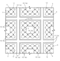
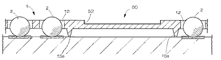
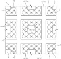
上記問題を解消するために、本実施形態に係るマスク1は、通孔12からなるパターン領域の外周にピッチ調整部50を設けている。具体的には、図8に示すように、複数形成されたパターン領域間に開口51を設けることでピッチ調整部50を構成する。このように、パターン領域間にピッチ調整部50(開口51)を設けることにより、パターン領域間における磁力の作用が弱まって、マスク1にうねりが生じることを防止でき、半田ボール2を所望の位置に精度良く搭載することができる。これに加えて、マスク1の平面方向に張力を作用させれば、マスク1のうねりの発生をより効果的に抑えることができ、このことによっても精度良い半田ボール2の搭載に貢献できる。さらに、開口51をメッシュ状とすれば、伸長性に富む機能を備えることができるので、各パターン領域のピッチのズレを調整することができ、各パターン領域のパターンピッチ精度が良好となるとともに、マスク1をワーク3に対して追随性良く載置することができる。こうしたメッシュ状の開口51によってピッチ調整部50を構成する場合は、図9に示すように、隣接するパターン領域間における突起部15a間に設けると良い。なお、開口51によってピッチ調整部50を設ける場合、パターン領域間における開口率は10〜90%が好ましく、本実施形態では、開口率40%としたが、要はパターン領域間における開口率をパターン領域における開口率と同程度もしくはそれ以上とすれば良く、これにより、マスク1のうねりの発生を可及的に抑えることができるとともに、突起部15(15a・15b)をワーク3上に載置することができ、よって、精度良いボール搭載が可能となる。また、マスク1の平面方向に作用させる張力の大きさとしては、0.5〜2.0kg/cm2の範囲が好ましい。   In order to solve the above problem, the mask 1 according to the present embodiment is provided with a pitch adjusting unit 50 on the outer periphery of the pattern region including the through holes 12. Specifically, as shown in FIG. 8, the pitch adjusting unit 50 is configured by providing openings 51 between a plurality of formed pattern regions. As described above, by providing the pitch adjusting portion 50 (opening 51) between the pattern areas, the action of the magnetic force between the pattern areas is weakened, and it is possible to prevent the mask 1 from being swelled. Can be mounted with high accuracy. In addition to this, if tension is applied in the plane direction of the mask 1, the occurrence of waviness of the mask 1 can be suppressed more effectively, which can contribute to mounting of the solder balls 2 with high accuracy. Furthermore, if the opening 51 is mesh-shaped, it can be provided with a function rich in extensibility, so that the shift of the pitch of each pattern region can be adjusted, and the pattern pitch accuracy of each pattern region becomes good, The mask 1 can be placed on the workpiece 3 with good followability. When the pitch adjusting unit 50 is configured by such mesh-shaped openings 51, as shown in FIG. 9, the pitch adjusting unit 50 is preferably provided between the protruding portions 15a between adjacent pattern regions. In the case where the pitch adjusting unit 50 is provided by the openings 51, the aperture ratio between the pattern areas is preferably 10 to 90%. In the present embodiment, the aperture ratio is 40%, but the aperture ratio between the pattern areas is the pattern. The aperture ratio in the region may be equal to or higher than the aperture ratio, thereby suppressing the occurrence of waviness of the mask 1 as much as possible and placing the protrusions 15 (15a and 15b) on the workpiece 3. Therefore, accurate ball mounting is possible. Further, the magnitude of the tension acting in the plane direction of the mask 1 is preferably in the range of 0.5 to 2.0 kg / cm2.

ピッチ調整部50としては、隣り合うパターン領域間に凹部52を設ける形態としても良い。具体的には、図10に示すように、隣り合うパターン領域間におけるマスク本体10の厚みをパターン領域におけるマスク本体10の厚みより薄く形成している。係る構成によっても、パターン領域間における磁力の作用を小さくすることができ、マスク1にうねりが生じることを防止でき、半田ボール2を所望の位置に精度良く搭載することができる。もちろん、ピッチ調整部50として、開口51と凹部52とを組み合わせたものでも良い。このように、パターン領域間に作用させる磁力の大きさは、開口や凹部の形状・位置・数によって容易に調整することができる。   The pitch adjusting unit 50 may have a configuration in which the concave portion 52 is provided between adjacent pattern regions. Specifically, as shown in FIG. 10, the thickness of the mask body 10 between adjacent pattern regions is formed to be thinner than the thickness of the mask body 10 in the pattern regions. Even with such a configuration, it is possible to reduce the effect of the magnetic force between the pattern regions, to prevent the mask 1 from waviness, and to mount the solder ball 2 at a desired position with high accuracy. Of course, the pitch adjusting unit 50 may be a combination of the opening 51 and the recessed part 52. As described above, the magnitude of the magnetic force applied between the pattern regions can be easily adjusted by the shape, position, and number of openings and recesses.

ここで、ピッチ調整部50は、複数の開口51によって構成されるのが好ましく、さらに、この開口51は、半田ボール2が挿通できない形状・寸法とするのが好ましい。また、凹部52によってピッチ調整部50を設ける場合は、図11に示すように、マスク本体10(マスク1)のワーク3との対向面側に設けるのが好ましいが、図10に示すように、凹部52をマスク本体10(マスク1)の半田ボール2の供給側に設けた場合は、半田ボール滞留部として機能させることができる。なお、開口51を形成する方法としては、図6(b)に示す二次パターンレジストを形成する工程において、パターン領域の外周(パターン領域間)に対応する位置にレジスト体38aとは別のレジスト体を形成することで、容易に得られる。また、凹部52を形成する方法としては、図6(d)に示すマスク1において、パターン領域の外周(パターン領域間)に対応する位置にエッチングすることで、容易に得られる。凹部52は、プレスによっても形成することができる。この他のピッチ調整部50としては、図12に示すように、蛇腹状部53のものが考えられる。係るピッチ調整部50(開口51、凹部52、蛇腹状部53)は、全てのパターン領域間に設けなくても良く、要は予想されるマスク1のうねりに合わせて設ければ良い。また、ピッチ調整部50を構成する開口51、凹部52、蛇腹状部53は、組み合わせて設けても良い。   Here, the pitch adjusting unit 50 is preferably constituted by a plurality of openings 51, and the openings 51 are preferably shaped and dimensioned so that the solder balls 2 cannot be inserted therethrough. Moreover, when providing the pitch adjustment part 50 by the recessed part 52, as shown in FIG. 11, it is preferable to provide in the opposing surface side with the workpiece | work 3 of the mask main body 10 (mask 1), but as shown in FIG. When the concave portion 52 is provided on the supply side of the solder ball 2 of the mask body 10 (mask 1), it can function as a solder ball retention portion. In addition, as a method of forming the opening 51, in the step of forming the secondary pattern resist shown in FIG. 6B, a resist different from the resist body 38a at a position corresponding to the outer periphery of the pattern area (between the pattern areas). It is easily obtained by forming a body. Further, the method of forming the recess 52 can be easily obtained by etching the mask 1 shown in FIG. 6D at a position corresponding to the outer periphery of the pattern region (between the pattern regions). The recess 52 can also be formed by pressing. As the other pitch adjusting section 50, a bellows-shaped section 53 can be considered as shown in FIG. The pitch adjusting portion 50 (opening 51, concave portion 52, bellows-like portion 53) may not be provided between all the pattern regions, and may be provided according to the expected swell of the mask 1. Further, the opening 51, the concave portion 52, and the bellows-like portion 53 constituting the pitch adjusting portion 50 may be provided in combination.

(第2実施形態)
次に、第2実施形態に係る配列用マスクについて説明する。なお、上記構成と同一の部材には同一の符号を付してその説明を省略する。
(Second Embodiment)
Next, an array mask according to the second embodiment will be described. In addition, the same code | symbol is attached | subjected to the member same as the said structure, and the description is abbreviate | omitted.

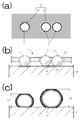
上記構成のマスク1においては、マスク本体10に形成された通孔12に1つの半田ボール2が投入される。ここで、例えば、ワーク3上に異なる2つの高さのバンプを形成する場合、フラックス印刷後、まず、バンプAとなる半田ボール2A(小ボール)が挿通できる通孔12Aを有するマスク1Aをワーク3上に載置して通孔12Aに半田ボール2Aを投入し、続いて、バンプBとなる半田ボール2B(大ボール)が挿通できる通孔12Bを有するマスク1Bをワーク3上に載置して通孔12Bに半田ボール2Bを投入して、加熱・溶融をしていた(バンプA・B、半田ボール2A・2B、通孔12A・12B、マスク1A・1Bは不図示)。このように、ワーク3上に異なる所望の高さのバンプを得るためには、異なるバンプの種類の数だけマスク及び工程が必要であった。   In the mask 1 having the above configuration, one solder ball 2 is put into the through hole 12 formed in the mask main body 10. Here, for example, when bumps of two different heights are formed on the workpiece 3, after the flux printing, a mask 1A having through holes 12A into which the solder balls 2A (small balls) to be the bumps A can be inserted is firstly mounted. 3, the solder balls 2 </ b> A are put into the through holes 12 </ b> A, and then the mask 1 </ b> B having the through holes 12 </ b> B into which the solder balls 2 </ b> B (large balls) to be the bumps B can be inserted is placed on the work 3. Then, the solder balls 2B were put into the through holes 12B and heated and melted (the bumps A and B, the solder balls 2A and 2B, the through holes 12A and 12B, and the masks 1A and 1B were not shown). As described above, in order to obtain bumps having different desired heights on the work 3, masks and processes corresponding to the number of different bump types are required.

上記問題を解消するために、本実施形態に係るマスク1は、図13(図13(a)は、本実施形態に係る配列用マスクの部分平面図、図13(b)は、その断面図)に示すように、ワーク3上における各半導体チップ5の電極6の配列パターンに対応した通孔12を備え、この通孔12は、単通孔13と、この単通孔13が複数連なった連続通孔14とを有する。そして、単通孔13は平面視で円形状に形成され、連続通孔14は単通孔13を2つ連ねた平面視でだるま状・ひょうたん状に形成されており、単通孔13には1つの半田ボール2を挿通でき、連続通孔14には2つの半田ボール2を挿通できる。ここで、係る構成のマスク1を用いて、例えば、直径200μmの半田ボール2を直径150μmの電極6に搭載した際のバンプの高さは、図13(c)に示すように、半田ボール2を1つ挿入した単通孔13におけるバンプ高さL1は172μmとなり、半田ボール2を2つ挿入した連続通孔14におけるバンプ高さL2は230μmとなった。この時、フラックス17は、連続通孔14に挿入されるそれぞれの半田ボール2が離れないように、ワーク3上に楕円状に印刷すると良い。   In order to solve the above problem, the mask 1 according to the present embodiment is shown in FIG. 13 (FIG. 13A is a partial plan view of the array mask according to the present embodiment, and FIG. 13B is a sectional view thereof. ), Through holes 12 corresponding to the arrangement pattern of the electrodes 6 of the respective semiconductor chips 5 on the work 3 are provided. The through holes 12 have a single through hole 13 and a plurality of the single through holes 13 connected to each other. And a continuous through hole 14. The single through-hole 13 is formed in a circular shape in plan view, and the continuous through-hole 14 is formed in a darling shape or gourd shape in plan view in which two single through-holes 13 are connected. One solder ball 2 can be inserted, and two solder balls 2 can be inserted into the continuous through hole 14. Here, for example, when the solder ball 2 having a diameter of 200 μm is mounted on the electrode 6 having a diameter of 150 μm by using the mask 1 having such a configuration, the height of the bump is as shown in FIG. The bump height L1 in the single through hole 13 with one inserted was 172 μm, and the bump height L2 in the continuous through hole 14 with two solder balls 2 inserted was 230 μm. At this time, the flux 17 is preferably printed in an elliptical shape on the workpiece 3 so that the solder balls 2 inserted into the continuous through holes 14 are not separated.

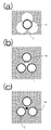
なお、連続通孔14は、連ねる単通孔13の数が3つ以上で構成されてあっても良い。この時、3つ以上の単通孔13を直線状に連ねて形成したものでも良いし、3つ以上の単通孔13をある点を中心にして円周状に連ねて形成した、いわゆる平面視でクローバー状のものでも良い。但し、例えば、連続通孔14が3つの単通孔13を円周状に連ねた形状(三つ葉のクローバー状)とする場合において、図14(a)に示すような形状であると、3つの単通孔13の中央に半田ボール2が挿入されてしまい、連続通孔14を構成するそれぞれの単通孔13に半田ボール2が挿入できないおそれがあるので、図14(b)に示すように、連続通孔14としての単通孔13の連なる部分は小さいほうが好ましい。また、図14(c)に示すように、連続通孔14は、これを構成する各単通孔13の円周が接するように連ねて形成されたものでも良い。ここで、連続通孔14の形状は、図13、図14(b)、図14(c)に示すように、その中央に電極6が位置するように形成するのが好ましい。また、連続通孔14を構成する一つの単通孔13の寸法は、電極6の寸法より大きく形成することが好ましい。そして、マスク1平面視の時に、連続通孔14(単通孔13)、半田ボール2、フラックス17、電極6の幅寸法は、連続通孔14(単通孔13)>半田ボール2>フラックス17>電極6の関係を満たすのが好ましい。   In addition, the continuous through-hole 14 may be comprised by the number of the single through-holes 13 connected 3 or more. At this time, it may be formed by connecting three or more single through holes 13 linearly, or a so-called plane formed by connecting three or more single through holes 13 in a circumferential shape around a certain point. A clover-shaped one may be used. However, for example, when the continuous through-hole 14 has a shape (three-leaf clover shape) in which three single through-holes 13 are arranged in a circle, the shape shown in FIG. Since the solder ball 2 is inserted into the center of the single through hole 13 and the solder ball 2 may not be inserted into each single through hole 13 constituting the continuous through hole 14, as shown in FIG. It is preferable that the continuous portion of the single through holes 13 as the continuous through holes 14 is small. Moreover, as shown in FIG.14 (c), the continuous through-hole 14 may be formed in a row so that the circumference | surroundings of each single through-hole 13 which comprises this may contact | connect. Here, the shape of the continuous through hole 14 is preferably formed so that the electrode 6 is positioned at the center thereof, as shown in FIGS. 13, 14 (b), and 14 (c). Moreover, it is preferable that the dimension of one single hole 13 constituting the continuous hole 14 is larger than the dimension of the electrode 6. When the mask 1 is viewed from above, the width of the continuous through hole 14 (single through hole 13), the solder ball 2, the flux 17, and the electrode 6 is as follows: continuous through hole 14 (single through hole 13)> solder ball 2> flux. 17> It is preferable that the relationship of the electrode 6 is satisfied.

このように、上記構成のマスク1を用意して半田ボール2の搭載作業を行うことで、ワーク3上に異なる所望の高さのバンプを形成することができるので、複数種のマスクを用意する必要がなくなり、コストの削減及びリードタイムの縮小が可能となる。そして、通孔12、すなわち、単通孔13及び連続通孔14の形状・寸法や連続通孔14を構成する単通孔13の数によって、バンプの高さを容易に調整・設定することができ、所望の高さのバンプを得ることができる。また、電極6の形状・寸法によっても、バンプの高さを調整・設定することができる。なお、所望形状の単通孔13及び連続通孔14を形成する方法としては、図6(b)に示す二次パターンレジストを形成する工程において、所望形状の単通孔13及び連続通孔14に対応したレジスト体38aを形成することで、容易に得られる。   As described above, by preparing the mask 1 having the above-described configuration and performing the mounting operation of the solder ball 2, bumps having different desired heights can be formed on the work 3, and thus a plurality of types of masks are prepared. This eliminates the need for cost and lead time. The height of the bump can be easily adjusted and set according to the shape and size of the through holes 12, that is, the single through holes 13 and the continuous through holes 14, and the number of the single through holes 13 constituting the continuous through holes 14. And a bump having a desired height can be obtained. Also, the height of the bump can be adjusted and set according to the shape and dimensions of the electrode 6. In addition, as a method of forming the single through hole 13 and the continuous through hole 14 having a desired shape, in the process of forming the secondary pattern resist shown in FIG. 6B, the single through hole 13 and the continuous through hole 14 having the desired shape. Can be easily obtained by forming the resist body 38a corresponding to the above.

上記各構成においては、突起部15が一体となったマスク1としているが、突起部15が別部材で一体的に形成されたものでも良い。これは上記マスク1において、例えば、マスク本体10を鉄、ニッケル等といった磁性体で形成し、突起部15を銅やアルミ等といった非磁性体で形成すれば、上述したように磁石(不図示)の磁力吸引力によってワーク3にマスク1を固定する場合に、マスク1に対して磁力が均一に働くことになるので、マスク1が不用意に撓むおそれがなく、電極6に対する通孔12の位置精度を向上することができる。   In each of the above-described configurations, the mask 1 is integrally formed with the protrusion 15, but the protrusion 15 may be formed integrally with another member. In the mask 1, for example, if the mask body 10 is formed of a magnetic material such as iron or nickel and the protrusion 15 is formed of a non-magnetic material such as copper or aluminum, a magnet (not shown) as described above. When the mask 1 is fixed to the work 3 by the magnetic attraction force, the magnetic force acts uniformly on the mask 1, so that the mask 1 is not inadvertently bent, and the through holes 12 for the electrodes 6 are not bent. Position accuracy can be improved.

また、突起部15を非磁性体で形成するものにおいて、金属に限らず樹脂によって形成したものであっても良い。これによれば、当該樹脂の弾力性に由来するクッション作用が発揮され、突起部15がワーク3に当接した際に、ワーク3が損傷するおそれが少なくなる。この効果を顕著に奏するために、マスク1においては、ワーク3と当接する全ての突起部15を樹脂で形成するのが好ましい。これによって、マスク1に対して磁力が均一に働くことにもなるので、マスク1が不用意に撓むおそれがなく、電極6に対する通孔12の位置精度を向上させることもできる。   Further, in the case where the protrusion 15 is formed of a non-magnetic material, it is not limited to metal but may be formed of resin. According to this, the cushion action derived from the elasticity of the resin is exhibited, and the possibility that the work 3 is damaged when the protrusion 15 contacts the work 3 is reduced. In order to achieve this effect remarkably, in the mask 1, it is preferable that all the protrusions 15 that come into contact with the workpiece 3 are made of resin. As a result, the magnetic force acts uniformly on the mask 1, so that the mask 1 is not inadvertently bent and the positional accuracy of the through-hole 12 with respect to the electrode 6 can be improved.

また、突起部15の下端面の形状は、円に限らず、楕円でも良いし、四角・ひし形・六角形などといった多角形でも良い。さらに、これら形状を構成する角や突起部15の下端面と側面との境界部分は、R状とするのが好ましい。これにより、例えば、マスク1の突起部15形成面を洗浄する際に、洗浄をスムーズに行うことができるとともに、洗浄手段(布やスポンジなど)が突起部15に引っかかることによる洗浄手段及び突起部15の破損のおそれを可及的に防止することができる。   Further, the shape of the lower end surface of the protrusion 15 is not limited to a circle, and may be an ellipse or a polygon such as a square, a rhombus, or a hexagon. Furthermore, it is preferable that the corners constituting these shapes and the boundary portion between the lower end surface and the side surface of the protrusion 15 have an R shape. Accordingly, for example, when the surface of the mask 1 where the protrusion 15 is formed can be cleaned, the cleaning can be performed smoothly, and the cleaning means and the protrusion due to the cleaning means (cloth, sponge, etc.) being caught by the protrusion 15. The risk of damage to 15 can be prevented as much as possible.

1 配列用マスク
2 半田ボール
3 ワーク
6 電極
10 マスク本体
12 通孔
13 単通孔
14 連続通孔
15 突起部
15a 突起部
15b 突起部
30 母型
31 フォトレジスト層
34 一次パターンレジスト
35 一次電鋳層
36 フォトレジスト層
38 二次パターンレジスト
39 二次電鋳層
50 ピッチ調整部
51 開口
52 凹部
53 蛇腹状部
DESCRIPTION OF SYMBOLS 1 Mask for arrangement | sequence 2 Solder ball 3 Workpiece 6 Electrode 10 Mask main body 12 Through-hole 13 Single through-hole 14 Continuous through-hole 15 Protrusion part 15a Protrusion part 15b Protrusion part 30 Master mold 31 Photoresist layer 34 Primary pattern resist 35 Primary electroformed layer 36 Photoresist layer 38 Secondary pattern resist 39 Secondary electroformed layer 50 Pitch adjusting part 51 Opening 52 Recessed part 53 Bellows part

Claims (3)

所定の配列パターンに対応した通孔(12)内に半田ボール(2)を振り込むことで、ワーク(3)上の所定位置に前記半田ボール(2)を搭載する配列用マスクであって、
前記通孔(12)からなるパターン領域が多数形成されたマスク本体(10)と、前記マスク本体(10)の前記ワーク(3)との対向面側に設けられた突起部(15)とを備え、
前記突起部(15)が前記パターン領域間に形成されており、
前記パターン領域間にピッチ調整部(50)を構成する凹部(52)または蛇腹状部(53)を設け磁力の作用を弱めることを特徴とする配列用マスク。
An array mask for mounting the solder balls (2) at predetermined positions on the workpiece (3) by swinging the solder balls (2) into the through holes (12) corresponding to the predetermined array pattern,
A mask main body (10) in which a large number of pattern regions including the through holes (12) are formed, and a protrusion (15) provided on the surface of the mask main body (10) facing the workpiece (3). Prepared,
The protrusion (15) is formed between the pattern regions;
Sequence mask, characterized in that weaken the magnetic force provided recessed portions that make up the pitch adjustment section (50) to (52) or the bellows portion (53) between said pattern area.
前記突起部(15)が前記パターン領域を囲むように前記パターン領域ごとに形成されており、前記ピッチ調整部(50)は、前記パターン領域間、且つ前記突起部(15)間に設けられていることを特徴とする請求項1に記載の配列用マスク。   The protrusion (15) is formed for each pattern region so as to surround the pattern region, and the pitch adjusting portion (50) is provided between the pattern regions and between the protrusions (15). The array mask according to claim 1, wherein the mask is an array mask. 前記通孔(12)や前記突起部(15)の形状がテーパ状であることを特徴とする請求項1または2に記載の配列用マスク。   3. The arrangement mask according to claim 1, wherein the through holes (12) and the protrusions (15) are tapered.
JP2014112483A 2012-03-26 2014-05-30 Mask for array Active JP6202575B2 (en)

Priority Applications (1)

Application Number Priority Date Filing Date Title
JP2014112483A JP6202575B2 (en) 2012-03-26 2014-05-30 Mask for array

Applications Claiming Priority (3)

Application Number Priority Date Filing Date Title
JP2012068600 2012-03-26
JP2014112483A JP6202575B2 (en) 2012-03-26 2014-05-30 Mask for array

Related Parent Applications (1)

Application Number Title Priority Date Filing Date
JP2013044066A Division JP2013229577A (en) 2012-03-26 2013-03-06 Mask for arrangement

Publications (2)

Publication Number Publication Date
JP2014197694A JP2014197694A (en) 2014-10-16
JP6202575B2 true JP6202575B2 (en) 2017-09-27

Family

ID=49676881

Family Applications (2)

Application Number Title Priority Date Filing Date
JP2013044066A Pending JP2013229577A (en) 2012-03-26 2013-03-06 Mask for arrangement
JP2014112483A Active JP6202575B2 (en) 2012-03-26 2014-05-30 Mask for array

Family Applications Before (1)

Application Number Title Priority Date Filing Date
JP2013044066A Pending JP2013229577A (en) 2012-03-26 2013-03-06 Mask for arrangement

Country Status (1)

Country Link
JP (2) JP2013229577A (en)

Families Citing this family (4)

* Cited by examiner, † Cited by third party
Publication number Priority date Publication date Assignee Title
JP6381322B2 (en) * 2014-07-07 2018-08-29 マクセルホールディングス株式会社 Mask for array
TW201602715A (en) * 2014-07-07 2016-01-16 Hitachi Maxell Mask for arrangement and the manufacturing method of the same
JP6456229B2 (en) * 2015-04-20 2019-01-23 マクセルホールディングス株式会社 Solder ball suction mask and method of manufacturing the same
KR101699722B1 (en) * 2016-04-15 2017-01-25 정병식 A method of repair SBA TOOL

Family Cites Families (3)

* Cited by examiner, † Cited by third party
Publication number Priority date Publication date Assignee Title
JP4282724B2 (en) * 2007-02-20 2009-06-24 日本テキサス・インスツルメンツ株式会社 Transfer mask for micro ball mounter
JP5046719B2 (en) * 2007-04-12 2012-10-10 日立マクセル株式会社 Mask for array and manufacturing method thereof
JP5156118B2 (en) * 2011-09-29 2013-03-06 日立マクセル株式会社 Mask for array

Also Published As

Publication number Publication date
JP2013229577A (en) 2013-11-07
JP2014197694A (en) 2014-10-16

Similar Documents

Publication Publication Date Title
JP6150500B2 (en) Mask for array
JP6202575B2 (en) Mask for array
JP2009182068A (en) Mask for array and method of manufacturing the same
JP5046719B2 (en) Mask for array and manufacturing method thereof
JP7326541B2 (en) array mask
JP5905756B2 (en) Alignment mask and solder bump forming method
JP6277239B2 (en) Mask for array
JP7392079B2 (en) array mask
JP4798631B2 (en) Solder ball arrangement mask and manufacturing method thereof
JP6758108B2 (en) Mask for arranging conductive pillars and its manufacturing method
JP5156118B2 (en) Mask for array
JP6381322B2 (en) Mask for array
JP5190880B2 (en) Solder ball arrangement mask and manufacturing method thereof
JP5838436B1 (en) Conductive ball placement mask and method of manufacturing the same
JP2020047947A (en) Solder ball alignment mask and manufacturing method thereof
JP6963769B2 (en) Metal mask and its manufacturing method
JP6456229B2 (en) Solder ball suction mask and method of manufacturing the same
JP2018170529A (en) Mask for arrangement
JP7473705B2 (en) Array Mask
JP6636118B2 (en) Mask for arranging solder balls and method of manufacturing the same
JP2013190367A (en) Method for manufacturing membrane probe

Legal Events

Date Code Title Description
A621 Written request for application examination

Free format text: JAPANESE INTERMEDIATE CODE: A621

Effective date: 20151217

A977 Report on retrieval

Free format text: JAPANESE INTERMEDIATE CODE: A971007

Effective date: 20161122

A131 Notification of reasons for refusal

Free format text: JAPANESE INTERMEDIATE CODE: A131

Effective date: 20161125

A521 Request for written amendment filed

Free format text: JAPANESE INTERMEDIATE CODE: A523

Effective date: 20170120

A131 Notification of reasons for refusal

Free format text: JAPANESE INTERMEDIATE CODE: A131

Effective date: 20170131

A521 Request for written amendment filed

Free format text: JAPANESE INTERMEDIATE CODE: A523

Effective date: 20170328

TRDD Decision of grant or rejection written
A01 Written decision to grant a patent or to grant a registration (utility model)

Free format text: JAPANESE INTERMEDIATE CODE: A01

Effective date: 20170823

A61 First payment of annual fees (during grant procedure)

Free format text: JAPANESE INTERMEDIATE CODE: A61

Effective date: 20170823

R150 Certificate of patent or registration of utility model

Ref document number: 6202575

Country of ref document: JP

Free format text: JAPANESE INTERMEDIATE CODE: R150

S531 Written request for registration of change of domicile

Free format text: JAPANESE INTERMEDIATE CODE: R313531

S533 Written request for registration of change of name

Free format text: JAPANESE INTERMEDIATE CODE: R313533

R350 Written notification of registration of transfer

Free format text: JAPANESE INTERMEDIATE CODE: R350

R250 Receipt of annual fees

Free format text: JAPANESE INTERMEDIATE CODE: R250

R250 Receipt of annual fees

Free format text: JAPANESE INTERMEDIATE CODE: R250