JP6199638B2 - Plasma processing equipment - Google Patents
Plasma processing equipment Download PDFInfo
- Publication number
- JP6199638B2 JP6199638B2 JP2013147327A JP2013147327A JP6199638B2 JP 6199638 B2 JP6199638 B2 JP 6199638B2 JP 2013147327 A JP2013147327 A JP 2013147327A JP 2013147327 A JP2013147327 A JP 2013147327A JP 6199638 B2 JP6199638 B2 JP 6199638B2
- Authority
- JP
- Japan
- Prior art keywords
- wafer
- pin
- gas
- hole
- space
- Prior art date
- Legal status (The legal status is an assumption and is not a legal conclusion. Google has not performed a legal analysis and makes no representation as to the accuracy of the status listed.)
- Active
Links
Images


Description
本発明は、真空容器内の処理室内に設けた試料台に半導体ウエハ等の基板状の試料を配置し、処理室内に形成させたプラズマを用いて前記ウエハを処理するプラズマ処理装置に関するもので、特に、処理室内に置かれた試料台の温度を調節してウエハの温度を処理に適した温度に調整しつつこれを処理するプラズマ処理装置に関する。 The present invention relates to a plasma processing apparatus in which a substrate-like sample such as a semiconductor wafer is disposed on a sample stage provided in a processing chamber in a vacuum vessel, and the wafer is processed using plasma formed in the processing chamber. In particular, the present invention relates to a plasma processing apparatus for processing a wafer while adjusting the temperature of a sample stage placed in a processing chamber to adjust the temperature of a wafer to a temperature suitable for processing.
上記のようなプラズマ処理装置では、試料台上の半導体ウエハ等の試料の温度を調節しつつ試料が処理される。試料の温度は、一般的に試料台の温度調節により調整される。また、この温度調節のために試料を試料台上面に吸着させる目的で、試料台上に静電吸着用の電極を内部または下方面に有するセラミクス製の膜または板部材が配置されている。
試料台上のセラミクス製の膜または板部材および試料の接触面を完全な平坦にすることが困難であり、それぞれの面には微視的な凹凸が残っている。このため、これらの凹凸故に試料が試料台に密着せず、試料台上のセラミクス製の膜または板部材と試料との間に細隙が形成されることになる。この細隙にHe、Arなどの不活性なガスを導入することにより、接触不良による冷却ムラや加熱ムラが抑制され、ウエハ全体の温度が処理に適した温度に調整される。
In the plasma processing apparatus as described above, the sample is processed while adjusting the temperature of the sample such as a semiconductor wafer on the sample stage. The temperature of the sample is generally adjusted by adjusting the temperature of the sample stage. Further, for the purpose of adjusting the temperature, a ceramic film or plate member having an electrode for electrostatic attraction inside or on the lower surface is arranged on the sample table for the purpose of adsorbing the sample on the upper surface of the sample table.
It is difficult to completely flatten the contact surface between the ceramic film or plate member and the sample on the sample stage, and microscopic irregularities remain on each surface. For this reason, because of these irregularities, the sample does not adhere to the sample table, and a slit is formed between the ceramic film or plate member on the sample table and the sample. By introducing an inert gas such as He or Ar into the slit, uneven cooling and uneven heating due to poor contact are suppressed, and the temperature of the entire wafer is adjusted to a temperature suitable for processing.
このように、ガスを導入しウエハを温度調節する技術として、特開2002−305188号公報(特許文献1)、特開2010−153678号公報(特許文献2)がある。
特許文献1では、電極外周縁部およびその内側の複数箇所でそれぞれ開口する第1、第2ガス通路を設け、両者から熱伝導性ガス(反応性ガス)を供給し、ウエハを冷却させる技術が開示されている。
また、特許文献2では、ウエハを昇降させるピンが貫通する開口よりHeガスを導入する技術が開示され、ウエハが試料台の載置面上で吸着保持されている状態で、導入されたHeガスにより、ウエハの温度が局所的に異なりその温度分布の不均一を低減することを示唆している。
As described above, as a technique for adjusting the temperature of a wafer by introducing a gas, there are JP-A-2002-305188 (Patent Document 1) and JP-A-2010-153678 (Patent Document 2).
In Patent Document 1, a technique is provided in which first and second gas passages that open at an electrode outer peripheral edge and a plurality of locations inside the electrode are provided, a thermally conductive gas (reactive gas) is supplied from both, and the wafer is cooled. It is disclosed.
Patent Document 2 discloses a technique for introducing He gas through an opening through which a pin for raising and lowering a wafer passes, and the He gas introduced while the wafer is adsorbed and held on the mounting surface of the sample stage. This suggests that the temperature of the wafer is locally different and the unevenness of the temperature distribution is reduced.
上記の技術では、次の点について十分に考慮されていないため問題が生じていた。
すなわち、ウエハ面内で昇降させるピンが貫通する開口を覆う部分において、プラズマによりウエハが加熱され、ウエハ温度が適切な温度に調整されない点である。
そこで、本発明は、この問題点に鑑みてなされたもので、ウエハの温度分布を適切に制御して所望の温度に調整するものである。
The above-described technique has a problem because the following points are not fully considered.
That is, the wafer is heated by the plasma in the portion covering the opening through which the pins to be moved up and down in the wafer surface penetrate, and the wafer temperature is not adjusted to an appropriate temperature.
Therefore, the present invention has been made in view of this problem, and adjusts a wafer temperature distribution to a desired temperature by appropriately controlling the temperature distribution.
本発明は、真空処理室と、真空処理室に配置された試料台とを備え、真空処理室にプラズマを生成して試料台に載置したウエハにプラズマ処理を施すプラズマ処理装置において、試料台の上面に開口を有する上下方向に延びる複数の貫通孔を試料台に設け、これら貫通孔の内部で上下方向に移動しウエハの裏面と当接してウエハを試料台の上面から上方で昇降させる複数のピンと、これら貫通孔の下方の開口からピンの下部側の周囲を覆ってピンの上下の昇降に伴って伸縮し貫通孔の内側の空間を含むピンの周囲の空間を気密に封止して区画するベローズと、ピンおよびベローズの各下端部と連結して上下方向に駆動されピンを上下させるアーム部とを備え、ピンが貫通孔内に収納された状態で試料台の上面に載置されたウエハがプラズマを用いて処理されている間、アーム部に配置した供給口から所定範囲の温度に制御されたガスがベローズ内部のピンの周囲の空間内に導入されるようにしたことを特徴とする。 The present invention relates to a plasma processing apparatus that includes a vacuum processing chamber and a sample table disposed in the vacuum processing chamber, generates plasma in the vacuum processing chamber, and performs plasma processing on a wafer placed on the sample table. A plurality of vertically extending through holes having openings on the top surface of the sample base are provided in the sample table, and a plurality of holes are moved up and down inside the through holes to contact the back surface of the wafer and lift the wafer up and down from the top surface of the sample table. And the space around the pin including the space inside the through hole that expands and contracts as the pin moves up and down from the opening below the through hole to cover the lower part of the pin. It has a bellows that divides, and an arm part that is connected to the lower ends of the pin and bellows and is driven in the vertical direction to move the pin up and down, and the pin is placed on the upper surface of the sample stage in a state of being accommodated in the through hole. Wafer is plasma While being had to process, gas controlled from the supply port disposed on the arm portion to a temperature in the predetermined range, characterized in that it has to be introduced into the space around the pin inside the bellows.
本発明は、以上の構成を備えるため、ウエハを載置する試料台上面から上方でウエハに当接してウエハを昇降させるピンを内部に配置した貫通孔を覆うアーム部を冷却することにより、ウエハを所望の温度に調整することを可能にしたプラズマ処理装置を提供することができる。 Since the present invention has the above-described configuration, the wafer is cooled by cooling the arm portion that covers the through-hole in which the pins for moving the wafer up and down by contacting the wafer from the upper surface of the sample stage on which the wafer is placed are disposed. It is possible to provide a plasma processing apparatus that makes it possible to adjust the temperature to a desired temperature.
以下、本発明の実施形態として、実施例1および実施例2をそれぞれ添付図面を参照しながら説明する。 Hereinafter, as an embodiment of the present invention, Example 1 and Example 2 will be described with reference to the accompanying drawings.
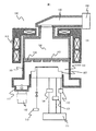
図1は、本実施例1に係るプラズマ処理装置の構成の概略を説明する縦断面図である。図1において、プラズマ処理装置100は、真空容器101、該真空容器上方の外周に配置されて真空容器101内部に電界および磁界を供給する電磁場供給手段、真空容器101内部を排気する排気手段とを備えた容器部、および、下方に該真空容器内部に電力やガス、冷却用冷媒等の流体を供給調節する制御装置を収納した直方体状を有するヘッド部、を備えることにより構成されている。
FIG. 1 is a longitudinal sectional view for explaining the outline of the configuration of the plasma processing apparatus according to the first embodiment. In FIG. 1, a
電磁波供給手段は、電波を発生させる電波源104、発生した電波をプラズマ処理室103に導く導波管105、導波管105に接続された共振器106、および、共振器106と真空容器101上部を取り囲むように配置されたソレノイドコイル112を備える。
The electromagnetic wave supply means includes a
電波源104は、マイクロ波やUHF波等の所定の周波数の電波を発生する。導波管105は、電波源104と共振器106に接続され、電波源104によって発生した電波を伝搬して共振器106内へ導く。共振器106は、円筒状であり、共振器106中央の上部で導波管105と接続される。共振器106の共振用の空間である共振室106’は、窓部材113をはさみ、プラズマ処理室103の直上に配置される。また、真空容器101上部と共振器106の外周を取り囲むように、リング状のソレノイドコイル112が複数段配置される。
The
真空容器101は、その上部にあって誘電体材料製の窓部材113、シャワープレート114、プラズマが形成される空間であって内側に配置された処理対象の試料が前記プラズマにより処理されるプラズマ処理室103、および、プラズマ処理室103の下部に配置されて試料がその上面に載せられて保持される試料台107を備える。
The
窓部材113は、石英誘電体製で円板状であり、共振器106の底面を構成し、共振器106およびプラズマ処理室103の間を気密に区画している。シャワープレート114は、石英等の誘電体製の円板であり、中央部に複数個の貫通孔が配置される。窓部材113の下方には、窓部材113と隙間を空けてシャワープレート114が並置される。シャワープレート114の下面は、プラズマ処理室103の天井面を構成する。シャワープレート114は、試料台107の上面と対向し並行して配置される。窓部材113およびシャワープレート114の隙間には、図示しないガス源から供給される処理用ガスを供給するための通路が設けられている。
The
プラズマ処理室103は、略円筒形状であって、処理対象の試料にプラズマ処理を施す際にプラズマが形成される空間である。また、プラズマ処理室103は、共振室106’の直下に位置し、内部に試料台107を備える。なお、プラズマ処理室103の内壁および試料台107の間の空間は、中心軸が合致したリング形状になっている。
The
試料台107は、少なくともバイアス電源108、試料台107の冷媒用温度調節器109、静電吸着用電源110、ガス供給部115と接続されている。バイアス電源108、試料台107の冷媒用温度調節器109および静電吸着用電源110は、コントローラ111により制御される。
The
試料台107の内部には導電性の電極が配置され、該電極は特定の高周波電力を供給するバイアス電源108と接続されている。また、試料台107の内部には冷媒溝が配置され、温度調節を行っている。
試料台107の上部には、試料の載置面を構成するAl2O3やY2O3等の誘電体材料で構成された誘電体膜が配置され、その内部には、ウエハを誘電体膜表面上に静電気力により吸着する静電吸着電極が配置されている。この静電吸着電極には、直流電力を供給する静電吸着電極用直流電源110が接続されている。
A conductive electrode is disposed inside the
A dielectric film made of a dielectric material such as Al 2 O 3 or Y 2 O 3 that constitutes a sample mounting surface is disposed on the upper part of the
真空容器101の下方には、排気手段であるターボ分子ポンプ等の真空ポンプ102が設置され、開口部117と連通している。
本実施例1のプラズマ処理装置100では、図示しない搬送部によりウエハをプラズマ処理室103の内部へ搬送し、プラズマ処理室103内に処理ガスを導入した後、プラズマ処理室103内にプラズマを生成し、生成されたプラズマにより前記ウエハを処理する。
Below the
In the
すなわち、プラズマ処理室103の内部は、真空ポンプ102によって排気され、減圧された状態にある。このとき、ウエハは、図示しないロボットアーム等の搬送手段により、図示しないゲートを通り試料台107上に搬送され、試料台107の載置面を構成する誘電体膜上に載せられる。その後、静電吸着電極用直流電源110から誘電体膜内の電極に電力が供給されることにより静電気力が形成され、ウエハは、この静電気力が形成された誘電体膜上に吸着されて保持される。
That is, the inside of the
ウエハが試料台107に保持された後、処理用ガスが図示しないガス源からシャワープレート114の貫通孔を通りプラズマ処理室103内に導入される。処理用ガスの流量と真空ポンプ102の動作による排気とのバランスにより、プラズマ処理室103の内部の圧力は所定の範囲に調節される。
After the wafer is held on the
処理用ガスの供給後に、電波源104は電波を発生させる。発生した電波は、導波管105を伝播して共振器106に導かれる。伝播した電波は、共振器内部106’で共振し、所定の強度の電界を形成する。この形成された電界は、窓部材113、シャワープレート114を透過してプラズマ処理室103に供給される。
ソレノイドコイル112には電流が供給され、プラズマ処理室103内に磁界が形成される。形成される磁界は、プラズマ処理室103の内側に上下方向の中心軸の周りに軸対象で下向き末広がりの形状である。
After supplying the processing gas, the
A current is supplied to the
このようにして形成された電界と磁場の相互作用により、処理用ガスを励起して、プラズマ処理室103内のウエハを保持した試料台107上方の空間にプラズマを形成する。
バイアス電源108からの高周波電力によって形成されたバイアス電位は、ウエハ表面にプラズマ中の荷電粒子を誘引して、ウエハ表面の処理対象の膜に物理的、化学的反応を生起させてエッチング等の処理を施す。
The processing gas is excited by the interaction between the electric field and the magnetic field thus formed, and plasma is formed in the space above the
The bias potential formed by the high frequency power from the
本実施例1では、プラズマの生成は、マイクロ波による電界と磁界との相互作用によるECRを用いたが、ECRに限定されるものではなく、高周波を用いた静電結合手段または誘導結合手段を用いたプラズマ生成手段を用いることも可能である。 In the first embodiment, the plasma is generated by using ECR based on the interaction between the electric field and the magnetic field by the microwave. However, the present invention is not limited to ECR, and electrostatic coupling means or inductive coupling means using a high frequency is used. It is also possible to use the plasma generating means used.
図2は、試料台107の構成を拡大して縦断面図として示すものである。試料台107は、2段以上の肩部を持った円板形状であり、Ti、セラミクス含有のアルミニウム、モリブデン、タングステン等の金属で構成される基材部203、基材部203の上面に接合されて、内部に図示されない金属の電極を備えた誘電体膜202を備える。基材部203の内部には、冷媒が内部を流れる基材冷媒溝204が設置されている。
FIG. 2 is an enlarged vertical sectional view showing the configuration of the
基材冷媒溝204は、冷媒が導入される入口および排出される出口が管路により、図1に示す真空容器101外部の冷媒用温度調節器109と連結されている。図1に示す冷媒用温度調節器109は、基材冷媒溝204を通り循環される冷媒の流量(速度)や冷媒の温度を図1に示すコントローラ111からの指令信号に応じて調節する。基材冷媒溝204の形状は、試料台107の上下方向の中心軸の回りに同心円またはら旋状に配置されている。冷媒は、基材冷媒溝204を流れ、基材部203を冷却する。基材部203が冷却されることで、試料台107に保持されたウエハ201が冷却される。
The base material
基材部203には、ガス導入部と連結した複数の貫通孔206、および、ウエハリフト用ピン252が貫通しかつガス導入部と連結した複数の貫通孔207が配置されている。本実施例1では、ガス導入部と連結した貫通孔は17個、ウエハリフト用ピン252が貫通する貫通孔は3個配置されている。これら貫通孔206および貫通孔207は、誘電体膜202も貫通して配置されている。
A plurality of through-
誘電体膜202は、Al2O3やY2O3等からなる溶射によって基材部203の上面に形成され、ブラストなどにより表面を所定の形状となるように成形される。また、内部には図示しない電極が配置され、図1に示す真空容器101の外部に設置された、図示しない直流電源に接続される。誘電体膜202の上面に形成される所定の形状として、外周に沿った土手、および、ウエハリフト用ピン252が貫通する貫通孔207の周囲に沿った土手が形成されている。これらの土手は、土手下面から土手上面までの高さが等しい、または等しいと見なせる高さに形成される。ウエハ201は、試料台107に保持された際、これらの土手により支持される。誘電体膜202の内部に配置された金属の電極に電圧が印加されることで、ウエハ201は誘電体膜に静電気力により吸着される。その際に、前記土手、ウエハ201の裏面および誘電体膜202の上面で形成された空間は、貫通孔206および貫通孔207から導入されるガスを一時的に保持することが可能である。
The
さらに、基材部203の下方には絶縁板205および金属ベース208が配置され、これらは、プラズマ処理室103とは内部および外部を気密に区画して内部を封止する機能を有している。本実施例1では、貫通孔206および貫通孔207は、絶縁板205および金属ベース208も貫通し配置されている。
Further, an insulating
基材部203には、図示されない高周波電力が印加されRFバイアスが形成されるので、絶縁板205で金属ベース208の間を電気絶縁している。金属ベース208より上方側は、プラズマ処理室103の内部側となり減圧された所定の真空度に維持され、金属ベース208より下方側は、大気圧等の大気圧空間となっている。金属ベース208は、図1に示す真空容器101の一部を構成するものである。
Since high frequency power (not shown) is applied to the
金属ベース208の下方には、アクチュエータ257、これと連結により接続されたアーム255、および、ウエハリフト用であってアーム255の端部に連結された上下方向に延在する棒状の複数個のウエハリフト用ピン252が配置されている。ウエハリフト用ピン252は、貫通孔207にこの通路の軸方向とその軸が並行になるように配置されている。
Below the
アクチュエータ257が駆動する上下の方向は、上記軸と平行または実質的にそれと見なせる程度に平行に配置され、アクチュエータ257の動作によりアーム255に連結されたウエハリフト用ピン252が連動して上下に移動される。このような動作は、後述の通り、プラズマ処理室103内のウエハ201の受け渡しに際して実施される。
The vertical direction in which the
各ウエハリフト用ピン252の下部の周囲は、蛇腹状を有して上下方向に伸縮可能な金属性のベローズフランジ254で覆われている。ベローズフランジ254は、その上端が金属ベース208の下面と連結され、その下端部がアーム255の上面と連結されている。これらの間にはOリング253が配置されており、ベローズフランジ254の内部と外部が気密に区別されている。これにより、貫通孔207を介してプラズマ処理室103と連通したベローズフランジ254の内側の空間は、減圧された状態で気密に封止可能に構成されている。
The periphery of the lower portion of each
本実施例1の貫通孔207の内壁面は、基材部203内に位置して、絶縁板205および金属ベース208を貫通する絶縁ボス251により構成されている。絶縁ボス251は、基材部203の内部に位置する上端部および金属ベース208を貫通する下部の外周面を囲んで当接するOリング253により封止されて、内周壁面の内部を隔離された空間にしている。
The inner wall surface of the through
各ベローズフランジ254により、区画された内部の空間に面したアーム255の上面には、Heガスのガス供給部115からバルブ260およびガス供給調整弁262が配置された経路を通り、Heガスを供給する開口259が配置されている。また、この経路はガス供給調整弁262と開口259との間でベローズフランジ254内部の開口259および誘電体膜202を貫通した貫通孔206と連通した各径路に分岐される。この内、開口259に到る経路は、アーム255の上下に応じて少なくとも一部が伸縮可能に構成されたフレキシブルチューブ258および配管264により構成されている。
By means of each bellows
ウエハ201が載置された状態で、これらを経由してHeガスが、ウエハ201の裏面、誘電体膜202の上面および誘電体膜202に形成された土手で隔離された空間と、ウエハ201の裏面およびウエハリフト用ピン252の周りのベローズフランジ254により隔離された空間に導入される。ウエハ201の裏面、誘電体膜202の上面および誘電体膜202に形成された土手で隔離された空間と、ウエハ201の裏面およびウエハリフト用ピン252の周りのベローズフランジ254により隔離された空間は、誘電体膜202上面に貫通孔207に沿って形成された土手により隔離されている。
In a state where the
ウエハ201の裏面、誘電体膜202の上面および誘電体膜202に形成された土手で隔離された空間に供給されるガスは、ガス供給調整弁261を通過して供給され、また、ウエハ201の裏面およびウエハリフト用ピン252の周りのベローズフランジ254により隔離された空間に供給されるガスは、ガス供給調整弁262を通過して供給される。そのため、ウエハ201の裏面、誘電体膜202の上面および誘電体膜202に形成された土手で隔離された空間と、ウエハ201の裏面およびウエハリフト用ピン252の周りのベローズフランジ254により隔離された空間、それぞれのガスの圧力は、異なる圧力で調整することも可能である。
The gas supplied to the back surface of the
フレキシブルチューブ258および配管264は、排気ポンプ265にバルブ263を介して接続されている。排気ポンプ265は、図1に示すプラズマ処理室103の排気ポンプ102と共通でもよい。ベローズフランジ254の内部に供給されたHeガスは、必要に応じて、バルブ263を開け排気される。
The
また、アーム255内部には、同心円またはアーム255の形状に沿ってアーム冷媒溝256が配置される。アーム冷媒溝256は、冷媒が導入される入口および排出される出口が管路により、図示されない真空容器101外部の温度調節器と接続されている。このアーム冷媒溝256と接続されている温度調節器は、前記した基材冷媒溝204と接続されている冷媒用温度調節器109と共通でもよいし、別途配置してもよい。本実施例1では、温度調節器は別途配置とした。
図示しない温度調節器からアーム冷媒溝256に導入された冷媒は、アーム冷媒溝256を通りアーム255を冷却する。アーム255が冷却されることで、アーム255と接続したウエハリフト用ピン252が冷却される。この冷却されたウエハリフト用ピン252により、開口259から導入されたHeガスを冷却する。開口259から導入され冷却されたHeガスにより、試料台107に載置されたウエハ201の貫通孔207を覆う部分が冷却される。
In addition, an arm
The refrigerant introduced into the arm
このような試料台107に対して、所定の処理を受ける対象のウエハ201は、図示しないロボットに載せられた状態で搬送され、図示しないゲートを通り、試料台107の上方に達した位置でロボットの動作を停止して、ウエハ201が試料台107の上方で保持される。
A
アクチュエータ257が駆動され、ウエハリフト用ピン252が上方に移動し、その上端部が誘電体膜202の貫通孔207から上方に上昇する。さらに、ウエハ201の裏面と当接してウエハ201を上端部に載せてロボットから上方に持ち上げるまでウエハリフト用ピン252の上部をロボット上方に上昇させ所定の上端位置でこれを保持する。この状態が維持されてロボットが処理室100の外部へ退避した後、アクチュエータ257の動作によりウエハリフト用ピン252が下方に移動してウエハ201の裏面が誘電体膜202の上面に形成された土手と接してから更に下方に通路内を下端位置まで移動する。その後、誘電体膜202の内部に配置された金属の電極に図示しない静電吸着用電源から電力が印加され静電気力が形成された誘電体膜202上に、ウエハ201は吸着されて保持される。
基材冷媒溝204には、所定の温度および流量に制御された冷媒が入口から導入され出口より排出されることで、基材部203を所定の温度に保持している。アーム冷媒溝256にも、所定の温度および流量に制御された冷媒が入口から導入され出口より排出されることで、アーム255およびウエハリフト用ピン252を所定の温度に保持している。この時、アーム冷媒溝256に導入される冷媒の温度は、基材冷媒溝204に導入される温度以下であることが望ましい。
Refrigerant controlled to a predetermined temperature and flow rate is introduced into the base material
この状態で、ガス供給源115から、ガスバルブ260によりガス供給量を調節するガス供給調整弁261またはガス供給調整弁262を通り、誘電体膜202を貫通する貫通孔206および貫通孔207を介して、ウエハ201の裏面および誘電体膜202の上面で構成される空間にHeガスを供給してウエハ201を冷却する。
In this state, the
この時、ウエハ201の裏面およびウエハリフト用ピン252の周りのベローズフランジ254により隔離された空間の圧力は、ウエハ201の裏面、誘電体膜202の上面および誘電体膜202に形成された土手で隔離された空間の圧力より小さいことが望ましい。更に、ウエハ201の裏面、誘電体膜202の上面および誘電体膜202に形成された土手で隔離された空間の圧力は、1kPa〜3kPaで保持されること、また、ウエハ201の裏面およびウエハリフト用ピン252の周りのベローズフランジ254により隔離された空間の圧力は、1kPa〜4kPaで保持されること、がそれぞれ望ましい。
その後、所定の方法により発生されたプラズマにより、ウエハ201は処理される。
At this time, the pressure in the space isolated by the back surface of the
Thereafter, the
処理終了後、ウエハ201の裏面および誘電体膜202の上面で構成される空間に導入されたHeガスは、バルブ263または図示されない排気配管により排気される。ウエハ201の裏面および誘電体膜202の上面で構成される空間の圧力は、ウエハ201の表面と裏面とで圧力差がないと見なせる圧力に達するのが望ましい。
After the processing is completed, the He gas introduced into the space formed by the back surface of the
ウエハ201の表面と裏面との圧力差がないと見なせる状態になった後、誘電体膜202に配置された電極に印加された電力の供給が停止され、静電気力が低減され、除去される。この状態で再度アクチュエータ257が駆動されてウエハリフト用ピン252を貫通孔207の内部を上昇させて、その上端部のウエハ201を試料台107の上方に持上げてウエハリフト用ピン252の上端位置まで移動させる。
After reaching a state where there is no pressure difference between the front surface and the back surface of the
その後、図示しないゲートを通り、図示しないロボットが試料台107上方のウエハ201の下方に移動して停止後、アクチュエータ257の動作によりウエハリフト用ピン252がロボット下方まで移動して、ウエハ201をロボットに受け渡す。ロボットがゲートを通過し退避することで、ウエハ201はプラズマ処理室103の外部へと搬出される。
Thereafter, after passing through a gate (not shown), the robot (not shown) moves below the
図3に、図2に示す実施例1の別形例である実施例2を図示する。図2に示した実施例1と本実施例2との構成上の相違点は、アーム255には冷媒溝を配置せず、熱交換器270にて温度調節されたHeガスをアーム255に配置した開口272から導入し、この開口272とは別に排気ポンプ265と連通した開口273をアーム255に配置している点である。
FIG. 3 shows a second embodiment which is a modified example of the first embodiment shown in FIG. The difference in configuration between the first embodiment shown in FIG. 2 and the second embodiment is that the
開口272および開口273は、各ベローズフランジ254の内部に連通している。また、アーム255には実施例1で使用したウエハリフト用ピン252は配置されず、替わってウエハリフト用中空ピン271が配置され、ウエハ201の受け渡しにはウエハリフト用中空ピン271が使用される。ウエハリフト用中空ピン271は、円筒形状であり、内部にガスを導入可能に構成され、開口部272と連通されている。
The
図2に示すように、ベローズフランジ254により区画された内部の空間に面したアーム255の上面には、Heガスのガス供給部115からバルブ260、ガス供給調整弁262を介し(図2では図示せず)、熱交換器270が配置された経路を通り、Heガスが供給される開口272が配置されている。この開口272の周囲には土手が形成され、この土手の内部の上方とウエハリフト用中空ピン271の外側の下方とがOリングにより当接している。これにより、Heガスは、熱交換器270により所定の温度に調整された後、開口272から導入され、ウエハリフト用中空ピン271の内部を通過した後、ベローズフランジ254により区画された内部の空間に導入され、試料台107に載置されたウエハ201の貫通孔207を覆う部分を冷却する。ここで、ウエハリフト用中空ピン271の上端は、試料台107に載置されたウエハ201の裏面と0.5mm以下の隙間となるように調整されていることが望ましい。そして、ガス供給部115から開口272までの経路は、アーム255の上下の動きに応じて少なくとも一部が伸縮可能に構成されたフレキシブルチューブ258、および、配管264により構成されている。
As shown in FIG. 2, the upper surface of the
また、アーム255の上面には、圧力調整弁266から排気ポンプ265に続く経路によりガスを排気する開口273が設置されている。誘電体膜202の上面にウエハ201が載置されている場合、開口272より導入されウエハリフト用中空ピン271を通過するHeガスは、開口273を通過して排気される。圧力調整弁266は、ウエハ201の裏面とベローズフランジ254とで区画される空間を所定の圧力となるように調整する。
In addition, an
このような構成により、Heガスが、ウエハリフト用中空ピン271から導入され、ベローズフランジ254の内部に充填され、圧力調整弁266により排気される。ベローズフランジ254の内部は、圧力調整弁266により1kPa〜4kPa程度の圧力になるように、排気ガスの流量が調整される。
With such a configuration, He gas is introduced from the wafer lift
同一空間で同一のガスであるときにガス内で温度分布がある場合、高温側のガスは上方に分散し、低温側のガスは下方に分散する。そのため、ウエハ201の冷却のため、冷却したHeガスがアーム255の開口部272から導入され、ベローズフランジ254の内部に充填する場合には、暖められたHeガスがウエハ裏面に多く充填されることになる。
When there is a temperature distribution in the same gas in the same space, the high temperature side gas is dispersed upward and the low temperature side gas is dispersed downward. Therefore, when the cooled He gas is introduced from the
ウエハ201の搬送時に、ウエハ201を試料台107より上部に持ち上げるウエハリフト用ピンは、一般に、ストロークを短くするため、そのピンの上端がウエハ201の近傍となるように設置される。図3に示す実施例2に示す通り、Heガスがウエハリフト用中空ピン271の上端からベローズフランジ254の内部に導入されることで、Heガスがアーム255の開口272から直に導入される場合よりも、効率よくウエハを冷却することが可能となる。
Wafer lift pins that lift the
100 プラズマ処理装置
101 真空容器
102 ターボ分子ポンプ等の真空ポンプ
103 プラズマ処理室
104 電波源
105 導波管
106 共振容器
107 試料台
108 バイアス電源
109 冷媒用温度調節器
110 静電吸着電極用直流電源
111 制御部であるコントローラ
112 ソレノイドコイル
113 円板状の窓部材
114 シャワープレート
115 ガス供給部
117 開口部
201 ウエハ
202 誘電体膜
203 基材部
204 基材冷媒溝
205 絶縁板
206、207 貫通孔
208 金属ベース
251 絶縁ボス
252 ウエハリフト用ピン
253、274 Oリング
254 ベローズフランジ
255 アーム
256 アーム冷媒溝
257 アクチュエータ
258 フレキシブルチューブ
259 開口
260、263 バルブ
261、262 ガス供給調整弁
264 配管
265 排気ポンプ
266 圧力調整弁
270 熱交換器
271 ウエハリフト用中空ピン
272、273 開口部
DESCRIPTION OF
Claims (3)
前記処理室内に配置され処理対象のウエハが載置される上面を有する試料台と、
前記試料台に配置され前記上面に開口を有する上下方向に延びる複数の貫通孔と、
前記複数の貫通孔の内部に配置され上下方向に移動し前記ウエハの裏面と当接して当該ウエハを前記試料台の上面から上方で昇降させる複数のピンと、
前記貫通孔の下方の開口から前記ピンの下部側の周囲を覆って前記ピンの上下の昇降に伴って伸縮し前記貫通孔の内側の空間を含む前記ピンの周囲の空間を気密に封止して区画するベローズと、
前記ピンおよび前記ベローズの各下端部と連結して上下方向に駆動され前記ピンを上下させるアーム部と、
を備え、
前記アーム部は、前記ピンが前記貫通孔内に収納された状態で前記試料台の上面に載置された前記ウエハが前記プラズマを用いて処理されている間、所定範囲の温度に制御されたガスが前記ベローズ内部の前記ピンの周囲の空間内に導入される供給口を該空間に面して配置すると共に、自らの内部に前記ガスの温度を調節する温度調節部を設けた
ことを特徴とするプラズマ処理装置。 A processing chamber in which a plasma is formed in its inner portion disposed inside the vacuum vessel,
A sample table having an upper surface on which the wafer is Ru is placed to be processed disposed in the processing chamber,
A plurality of through-holes arranged in the sample stage and extending in the vertical direction having an opening on the upper surface;
A plurality of pins that are arranged inside the plurality of through-holes and move up and down to contact the back surface of the wafer and raise and lower the wafer from the upper surface of the sample table;
Covering the periphery of the lower side of the pin from the opening below the through-hole, the space around the pin including the space inside the through-hole is hermetically sealed by expanding and contracting as the pin moves up and down. The bellows
An arm portion that is connected to the lower end portions of the pin and the bellows and is driven in the vertical direction to move the pin up and down,
With
The arm portion is controlled to a temperature within a predetermined range while the wafer placed on the upper surface of the sample stage with the pin being accommodated in the through hole is processed using the plasma. the supply port gas is introduced into the space around the pin inside the bellows together arranged facing the space, providing the temperature adjusting unit for adjusting the temperature of its interior to the gas <br A plasma processing apparatus characterized by the above.
前記処理室内に配置され処理対象のウエハが載置される上面を有する試料台と、
前記試料台に配置され前記上面に開口を有する上下方向に延びる複数の貫通孔と、
前記複数の貫通孔の内部に配置され上下方向に移動し前記ウエハの裏面と当接して当該ウエハを前記試料台の上面から上方で昇降させる複数のピンと、
前記貫通孔の下方の開口から前記ピンの下部側の周囲を覆って前記ピンの上下の昇降に伴って伸縮し前記貫通孔の内側の空間を含む前記ピンの周囲の空間を気密に封止して区画するベローズと、
前記ピンおよび前記ベローズの各下端部と連結して上下方向に駆動され前記ピンを上下させるアーム部と、
を備え、
前記アーム部は、前記ピンが前記貫通孔内に収納された状態で前記試料台の上面に載置された前記ウエハが前記プラズマを用いて処理されている間、所定範囲の温度に制御されたガスが前記ベローズ内部の前記ピンの周囲の空間内に導入される供給口を該空間に面して配置し、
前記ピンは、自らの先端から上方に向けて開放されたガス孔を設けた中空ピンで構成され、前記所定範囲の温度に制御されたガスは前記供給口を介して前記ガス孔から前記空間内に供給される
ことを特徴とするプラズマ処理装置。 A processing chamber that is placed inside the vacuum vessel and in which plasma is formed;
A sample stage disposed in the processing chamber and having a top surface on which a wafer to be processed is placed;
A plurality of through-holes arranged in the sample stage and extending in the vertical direction having an opening on the upper surface;
A plurality of pins that are arranged inside the plurality of through-holes and move up and down to contact the back surface of the wafer and raise and lower the wafer from the upper surface of the sample table;
Covering the periphery of the lower side of the pin from the opening below the through-hole, the space around the pin including the space inside the through-hole is hermetically sealed by expanding and contracting as the pin moves up and down. The bellows
An arm portion that is connected to the lower end portions of the pin and the bellows and is driven in the vertical direction to move the pin up and down,
With
The arm portion is controlled to a temperature within a predetermined range while the wafer placed on the upper surface of the sample stage with the pin being accommodated in the through hole is processed using the plasma. A supply port through which gas is introduced into the space around the pin inside the bellows is arranged facing the space,
The pin is configured by a hollow pin provided with a gas hole opened upward from its tip, and the gas controlled to a temperature within the predetermined range passes through the supply port from the gas hole into the space. the plasma processing apparatus according to claim <br/> be supplied to.
前記アーム部は、前記ガス孔の下方に配置され前記ベローズ内部の前記ピンの周囲の空間に面したガス排気口を設けた
ことを特徴とするプラズマ処理装置。
The plasma processing apparatus according to claim 2 ,
The plasma processing apparatus , wherein the arm portion is provided with a gas exhaust port disposed below the gas hole and facing a space around the pin inside the bellows .
Priority Applications (1)
| Application Number | Priority Date | Filing Date | Title |
|---|---|---|---|
| JP2013147327A JP6199638B2 (en) | 2013-07-16 | 2013-07-16 | Plasma processing equipment |
Applications Claiming Priority (1)
| Application Number | Priority Date | Filing Date | Title |
|---|---|---|---|
| JP2013147327A JP6199638B2 (en) | 2013-07-16 | 2013-07-16 | Plasma processing equipment |
Publications (2)
| Publication Number | Publication Date |
|---|---|
| JP2015023041A JP2015023041A (en) | 2015-02-02 |
| JP6199638B2 true JP6199638B2 (en) | 2017-09-20 |
Family
ID=52487279
Family Applications (1)
| Application Number | Title | Priority Date | Filing Date |
|---|---|---|---|
| JP2013147327A Active JP6199638B2 (en) | 2013-07-16 | 2013-07-16 | Plasma processing equipment |
Country Status (1)
| Country | Link |
|---|---|
| JP (1) | JP6199638B2 (en) |
Cited By (1)
| Publication number | Priority date | Publication date | Assignee | Title |
|---|---|---|---|---|
| JP7172936B2 (en) | 2019-09-27 | 2022-11-16 | Jfeエンジニアリング株式会社 | Garbage sorting method and device |
Families Citing this family (9)
| Publication number | Priority date | Publication date | Assignee | Title |
|---|---|---|---|---|
| JP6804836B2 (en) * | 2015-11-17 | 2020-12-23 | 株式会社日立ハイテク | Vacuum processing equipment |
| JP6863784B2 (en) * | 2017-03-16 | 2021-04-21 | 株式会社Screenホールディングス | Board processing equipment |
| KR20190056552A (en) * | 2017-11-17 | 2019-05-27 | 세메스 주식회사 | A supporting unit and an apparatus for processing substrates with the supporting unit |
| JP7002357B2 (en) * | 2018-02-06 | 2022-01-20 | 株式会社日立ハイテク | Plasma processing equipment |
| JP7083463B2 (en) * | 2018-02-23 | 2022-06-13 | 株式会社日立ハイテク | Vacuum processing equipment |
| CN110896045B (en) * | 2018-09-12 | 2022-12-30 | 中微半导体设备(上海)股份有限公司 | Lifting thimble assembly, electrostatic chuck and processing device with electrostatic chuck |
| KR102398674B1 (en) * | 2019-06-10 | 2022-05-17 | 세메스 주식회사 | A support unit, a substrate processing apparatus including the same, and a substrate processing method |
| JP2022014522A (en) * | 2020-07-07 | 2022-01-20 | 東京エレクトロン株式会社 | Vacuum processing device and control method of the same |
| CN117577575A (en) * | 2024-01-16 | 2024-02-20 | 北京北方华创微电子装备有限公司 | Bearing device and semiconductor process equipment |
Family Cites Families (6)
| Publication number | Priority date | Publication date | Assignee | Title |
|---|---|---|---|---|
| JP3167820B2 (en) * | 1993-01-29 | 2001-05-21 | 東京エレクトロン株式会社 | Abnormal discharge detection method |
| JP3600271B2 (en) * | 1994-05-25 | 2004-12-15 | 東京エレクトロン株式会社 | Processing equipment |
| US20050000450A1 (en) * | 2001-10-16 | 2005-01-06 | Iizuka Hachishiro | Treatment subject elevating mechanism, and treating device using the same |
| JP4712614B2 (en) * | 2006-05-29 | 2011-06-29 | 株式会社アルバック | Vacuum processing equipment |
| JP4372182B2 (en) * | 2007-08-02 | 2009-11-25 | 東京エレクトロン株式会社 | Substrate support mechanism, reduced-pressure drying apparatus, and substrate processing apparatus |
| JP5188385B2 (en) * | 2008-12-26 | 2013-04-24 | 株式会社日立ハイテクノロジーズ | Plasma processing apparatus and method of operating plasma processing apparatus |
-
2013
- 2013-07-16 JP JP2013147327A patent/JP6199638B2/en active Active
Cited By (1)
| Publication number | Priority date | Publication date | Assignee | Title |
|---|---|---|---|---|
| JP7172936B2 (en) | 2019-09-27 | 2022-11-16 | Jfeエンジニアリング株式会社 | Garbage sorting method and device |
Also Published As
| Publication number | Publication date |
|---|---|
| JP2015023041A (en) | 2015-02-02 |
Similar Documents
| Publication | Publication Date | Title |
|---|---|---|
| JP6199638B2 (en) | Plasma processing equipment | |
| KR102434559B1 (en) | Mounting table and plasma processing apparatus | |
| CN110120329B (en) | Plasma processing apparatus | |
| JP4255747B2 (en) | Plasma processing apparatus and plasma processing method | |
| CN111524850A (en) | Mounting table and substrate processing apparatus | |
| JP5591585B2 (en) | Plasma processing equipment | |
| KR101850355B1 (en) | Plasma processing apparatus | |
| JP2016046450A (en) | Plasma processing device | |
| JP4615464B2 (en) | Electrode assembly for plasma processing apparatus and plasma processing apparatus | |
| TWI498054B (en) | Antenna units, substrate treating apparatuses including the same, and substrate treating methods using the apparatuses | |
| JP4180637B2 (en) | Semiconductor manufacturing apparatus and semiconductor device manufacturing method | |
| KR20190072383A (en) | Plasma processing apparatus | |
| KR101898079B1 (en) | Plasma processing apparatus | |
| KR102050820B1 (en) | Substrate supporting unit and substrate treating apparatus including the unit | |
| KR101569904B1 (en) | Electrode assembly and apparatus and method fdr treating substrate | |
| KR101885102B1 (en) | Ntenna unit and substrate treating apparatus including the unit | |
| JP2019110312A (en) | Plasma processing method | |
| JP2020077759A (en) | Plasma processor | |
| US11587820B2 (en) | Mounting table, substrate processing apparatus, and control method | |
| JP6235293B2 (en) | Plasma processing equipment | |
| US11705346B2 (en) | Substrate processing apparatus | |
| WO2022230729A1 (en) | Substrate treatment device and substrate treatment method | |
| US20240079216A1 (en) | Apparatus for treating substrate and method for treating substrate | |
| KR102398674B1 (en) | A support unit, a substrate processing apparatus including the same, and a substrate processing method | |
| TW202412559A (en) | Apparatus for treating substrate and method for treating a substrate |
Legal Events
| Date | Code | Title | Description |
|---|---|---|---|
| A621 | Written request for application examination |
Free format text: JAPANESE INTERMEDIATE CODE: A621 Effective date: 20160704 |
|
| A977 | Report on retrieval |
Free format text: JAPANESE INTERMEDIATE CODE: A971007 Effective date: 20170313 |
|
| A131 | Notification of reasons for refusal |
Free format text: JAPANESE INTERMEDIATE CODE: A131 Effective date: 20170321 |
|
| A521 | Written amendment |
Free format text: JAPANESE INTERMEDIATE CODE: A523 Effective date: 20170518 |
|
| TRDD | Decision of grant or rejection written | ||
| A01 | Written decision to grant a patent or to grant a registration (utility model) |
Free format text: JAPANESE INTERMEDIATE CODE: A01 Effective date: 20170801 |
|
| A61 | First payment of annual fees (during grant procedure) |
Free format text: JAPANESE INTERMEDIATE CODE: A61 Effective date: 20170824 |
|
| R150 | Certificate of patent or registration of utility model |
Ref document number: 6199638 Country of ref document: JP Free format text: JAPANESE INTERMEDIATE CODE: R150 |
|
| S531 | Written request for registration of change of domicile |
Free format text: JAPANESE INTERMEDIATE CODE: R313531 |
|
| S533 | Written request for registration of change of name |
Free format text: JAPANESE INTERMEDIATE CODE: R313533 |
|
| R350 | Written notification of registration of transfer |
Free format text: JAPANESE INTERMEDIATE CODE: R350 |