JP6182021B2 - Power converter - Google Patents
Power converter Download PDFInfo
- Publication number
- JP6182021B2 JP6182021B2 JP2013176323A JP2013176323A JP6182021B2 JP 6182021 B2 JP6182021 B2 JP 6182021B2 JP 2013176323 A JP2013176323 A JP 2013176323A JP 2013176323 A JP2013176323 A JP 2013176323A JP 6182021 B2 JP6182021 B2 JP 6182021B2
- Authority
- JP
- Japan
- Prior art keywords
- overvoltage protection
- protection device
- filter capacitor
- power
- switching element
- Prior art date
- Legal status (The legal status is an assumption and is not a legal conclusion. Google has not performed a legal analysis and makes no representation as to the accuracy of the status listed.)
- Active
Links
Images


Classifications
-
- B—PERFORMING OPERATIONS; TRANSPORTING
- B60—VEHICLES IN GENERAL
- B60L—PROPULSION OF ELECTRICALLY-PROPELLED VEHICLES; SUPPLYING ELECTRIC POWER FOR AUXILIARY EQUIPMENT OF ELECTRICALLY-PROPELLED VEHICLES; ELECTRODYNAMIC BRAKE SYSTEMS FOR VEHICLES IN GENERAL; MAGNETIC SUSPENSION OR LEVITATION FOR VEHICLES; MONITORING OPERATING VARIABLES OF ELECTRICALLY-PROPELLED VEHICLES; ELECTRIC SAFETY DEVICES FOR ELECTRICALLY-PROPELLED VEHICLES
- B60L9/00—Electric propulsion with power supply external to the vehicle
- B60L9/02—Electric propulsion with power supply external to the vehicle using dc motors
- B60L9/04—Electric propulsion with power supply external to the vehicle using dc motors fed from dc supply lines
-
- B—PERFORMING OPERATIONS; TRANSPORTING
- B60—VEHICLES IN GENERAL
- B60L—PROPULSION OF ELECTRICALLY-PROPELLED VEHICLES; SUPPLYING ELECTRIC POWER FOR AUXILIARY EQUIPMENT OF ELECTRICALLY-PROPELLED VEHICLES; ELECTRODYNAMIC BRAKE SYSTEMS FOR VEHICLES IN GENERAL; MAGNETIC SUSPENSION OR LEVITATION FOR VEHICLES; MONITORING OPERATING VARIABLES OF ELECTRICALLY-PROPELLED VEHICLES; ELECTRIC SAFETY DEVICES FOR ELECTRICALLY-PROPELLED VEHICLES
- B60L15/00—Methods, circuits, or devices for controlling the traction-motor speed of electrically-propelled vehicles
-
- B—PERFORMING OPERATIONS; TRANSPORTING
- B60—VEHICLES IN GENERAL
- B60L—PROPULSION OF ELECTRICALLY-PROPELLED VEHICLES; SUPPLYING ELECTRIC POWER FOR AUXILIARY EQUIPMENT OF ELECTRICALLY-PROPELLED VEHICLES; ELECTRODYNAMIC BRAKE SYSTEMS FOR VEHICLES IN GENERAL; MAGNETIC SUSPENSION OR LEVITATION FOR VEHICLES; MONITORING OPERATING VARIABLES OF ELECTRICALLY-PROPELLED VEHICLES; ELECTRIC SAFETY DEVICES FOR ELECTRICALLY-PROPELLED VEHICLES
- B60L9/00—Electric propulsion with power supply external to the vehicle
- B60L9/16—Electric propulsion with power supply external to the vehicle using ac induction motors
- B60L9/18—Electric propulsion with power supply external to the vehicle using ac induction motors fed from dc supply lines
-
- B—PERFORMING OPERATIONS; TRANSPORTING
- B61—RAILWAYS
- B61C—LOCOMOTIVES; MOTOR RAILCARS
- B61C17/00—Arrangement or disposition of parts; Details or accessories not otherwise provided for; Use of control gear and control systems
-
- H—ELECTRICITY
- H02—GENERATION; CONVERSION OR DISTRIBUTION OF ELECTRIC POWER
- H02M—APPARATUS FOR CONVERSION BETWEEN AC AND AC, BETWEEN AC AND DC, OR BETWEEN DC AND DC, AND FOR USE WITH MAINS OR SIMILAR POWER SUPPLY SYSTEMS; CONVERSION OF DC OR AC INPUT POWER INTO SURGE OUTPUT POWER; CONTROL OR REGULATION THEREOF
- H02M7/00—Conversion of ac power input into dc power output; Conversion of dc power input into ac power output
- H02M7/42—Conversion of dc power input into ac power output without possibility of reversal
-
- H—ELECTRICITY
- H05—ELECTRIC TECHNIQUES NOT OTHERWISE PROVIDED FOR
- H05K—PRINTED CIRCUITS; CASINGS OR CONSTRUCTIONAL DETAILS OF ELECTRIC APPARATUS; MANUFACTURE OF ASSEMBLAGES OF ELECTRICAL COMPONENTS
- H05K7/00—Constructional details common to different types of electric apparatus
- H05K7/14—Mounting supporting structure in casing or on frame or rack
- H05K7/1422—Printed circuit boards receptacles, e.g. stacked structures, electronic circuit modules or box like frames
- H05K7/1427—Housings
- H05K7/1432—Housings specially adapted for power drive units or power converters
- H05K7/14325—Housings specially adapted for power drive units or power converters for cabinets or racks
-
- H—ELECTRICITY
- H05—ELECTRIC TECHNIQUES NOT OTHERWISE PROVIDED FOR
- H05K—PRINTED CIRCUITS; CASINGS OR CONSTRUCTIONAL DETAILS OF ELECTRIC APPARATUS; MANUFACTURE OF ASSEMBLAGES OF ELECTRICAL COMPONENTS
- H05K7/00—Constructional details common to different types of electric apparatus
- H05K7/14—Mounting supporting structure in casing or on frame or rack
- H05K7/1422—Printed circuit boards receptacles, e.g. stacked structures, electronic circuit modules or box like frames
- H05K7/1427—Housings
- H05K7/1432—Housings specially adapted for power drive units or power converters
- H05K7/14329—Housings specially adapted for power drive units or power converters specially adapted for the configuration of power bus bars
-
- H—ELECTRICITY
- H05—ELECTRIC TECHNIQUES NOT OTHERWISE PROVIDED FOR
- H05K—PRINTED CIRCUITS; CASINGS OR CONSTRUCTIONAL DETAILS OF ELECTRIC APPARATUS; MANUFACTURE OF ASSEMBLAGES OF ELECTRICAL COMPONENTS
- H05K7/00—Constructional details common to different types of electric apparatus
- H05K7/20—Modifications to facilitate cooling, ventilating, or heating
- H05K7/2089—Modifications to facilitate cooling, ventilating, or heating for power electronics, e.g. for inverters for controlling motor
- H05K7/20936—Liquid coolant with phase change
-
- B—PERFORMING OPERATIONS; TRANSPORTING
- B60—VEHICLES IN GENERAL
- B60L—PROPULSION OF ELECTRICALLY-PROPELLED VEHICLES; SUPPLYING ELECTRIC POWER FOR AUXILIARY EQUIPMENT OF ELECTRICALLY-PROPELLED VEHICLES; ELECTRODYNAMIC BRAKE SYSTEMS FOR VEHICLES IN GENERAL; MAGNETIC SUSPENSION OR LEVITATION FOR VEHICLES; MONITORING OPERATING VARIABLES OF ELECTRICALLY-PROPELLED VEHICLES; ELECTRIC SAFETY DEVICES FOR ELECTRICALLY-PROPELLED VEHICLES
- B60L2200/00—Type of vehicles
- B60L2200/26—Rail vehicles
-
- B—PERFORMING OPERATIONS; TRANSPORTING
- B60—VEHICLES IN GENERAL
- B60L—PROPULSION OF ELECTRICALLY-PROPELLED VEHICLES; SUPPLYING ELECTRIC POWER FOR AUXILIARY EQUIPMENT OF ELECTRICALLY-PROPELLED VEHICLES; ELECTRODYNAMIC BRAKE SYSTEMS FOR VEHICLES IN GENERAL; MAGNETIC SUSPENSION OR LEVITATION FOR VEHICLES; MONITORING OPERATING VARIABLES OF ELECTRICALLY-PROPELLED VEHICLES; ELECTRIC SAFETY DEVICES FOR ELECTRICALLY-PROPELLED VEHICLES
- B60L2210/00—Converter types
- B60L2210/40—DC to AC converters
-
- Y—GENERAL TAGGING OF NEW TECHNOLOGICAL DEVELOPMENTS; GENERAL TAGGING OF CROSS-SECTIONAL TECHNOLOGIES SPANNING OVER SEVERAL SECTIONS OF THE IPC; TECHNICAL SUBJECTS COVERED BY FORMER USPC CROSS-REFERENCE ART COLLECTIONS [XRACs] AND DIGESTS
- Y02—TECHNOLOGIES OR APPLICATIONS FOR MITIGATION OR ADAPTATION AGAINST CLIMATE CHANGE
- Y02T—CLIMATE CHANGE MITIGATION TECHNOLOGIES RELATED TO TRANSPORTATION
- Y02T10/00—Road transport of goods or passengers
- Y02T10/60—Other road transportation technologies with climate change mitigation effect
- Y02T10/72—Electric energy management in electromobility
Description
本発明は、電力変換装置に関し、特に鉄道車両用の電力変換装置に適用して好適なものである。 The present invention relates to a power converter, and is particularly suitable when applied to a power converter for a railway vehicle.
鉄道車両に設置される電力変換装置は、鉄道架線から入力される直流電力を複数のパワースイッチング素子により電力変換し、鉄道車両用の電動機に出力するものである。この電力変換装置は、主としてパワースイッチング素子と、パワースイッチング素子を冷却するための冷却ユニットと、鉄道架線から入力される直流電力の安定化を図るためのフィルタコンデンサとから構成される。 A power converter installed in a railway vehicle converts DC power input from a railway overhead line by a plurality of power switching elements and outputs the converted power to an electric motor for the railway vehicle. This power converter is mainly composed of a power switching element, a cooling unit for cooling the power switching element, and a filter capacitor for stabilizing DC power input from the railway overhead line.
特許文献1には、パワースイッチング素子にスナバ回路を並列に接続して構成される正側アームと、同様に構成される負側アームとを直列に接続して一相分のユニットを構成し、この一相分のユニットを3個用いてそれぞれを接続することにより、三相交流電圧を直流電圧に変換する電力変換装置が開示されている。 In Patent Literature 1, a positive-side arm configured by connecting a snubber circuit in parallel to a power switching element and a negative-side arm configured similarly are connected in series to form a unit for one phase, A power conversion device that converts a three-phase AC voltage into a DC voltage by connecting three units for one phase and connecting them is disclosed.
この特許文献1に記載の電力変換装置によれば、三相分のユニットを互いに接続する接続線を短くすることができるため、小さなスナバ回路容量であってもパワースイッチング素子にかかる高電圧を抑制することができるとしている。 According to the power conversion device described in Patent Document 1, since the connection lines connecting the units for three phases can be shortened, a high voltage applied to the power switching element is suppressed even with a small snubber circuit capacity. You can do that.
しかし、特許文献1に記載の電力変換装置におけるスナバ回路は、スナバ抵抗器、スナバダイオード及びスナバコンデンサから構成されており、特にスナバコンデンサを備えて構成されているため、重くてかさ張るものとなる。よって特許文献1に記載の構成では、電力変換装置の軽量化を図ることはできない。 However, the snubber circuit in the power conversion device described in Patent Document 1 is composed of a snubber resistor, a snubber diode, and a snubber capacitor, and is particularly heavy and bulky because it is configured with a snubber capacitor. Therefore, the configuration described in Patent Document 1 cannot reduce the weight of the power conversion device.
またスナバ回路は、上述したように重くてかさ張るものであるため、電力変換装置を収納する筐体内においてパワースイッチング素子とは別置きに設置する必要がある。スナバ回路をパワースイッチング素子とは別置きに設置すると、筐体内における機器のレイアウトに制約が生じる。よって電力変換装置の小型化を図ることはできない。 Further, since the snubber circuit is heavy and bulky as described above, it is necessary to install the snubber circuit separately from the power switching element in the housing that houses the power converter. If the snubber circuit is installed separately from the power switching element, there will be restrictions on the layout of the equipment in the housing. Therefore, the power converter cannot be downsized.
またスナバ回路とパワースイッチング素子とを別置きに設置すると、両者の間の配線が長くなり、一定以上長くなる場合には配線のインダクタンス成分を無視することができなくなる。この場合、この配線部分に誘導電圧が発生し、パワースイッチング素子を適正に保護することができない。 Further, if the snubber circuit and the power switching element are installed separately, the wiring between the two becomes long, and when the wiring becomes longer than a certain length, the inductance component of the wiring cannot be ignored. In this case, an induced voltage is generated in the wiring portion, and the power switching element cannot be properly protected.
本発明は以上の点を考慮してなされたものであり、軽量化及び小型化を図るとともに、パワースイッチング素子を適正に保護して信頼性の向上を実現し得る電力変換装置を提案するものである。 The present invention has been made in consideration of the above points, and proposes a power conversion device that can achieve weight reduction and downsizing and can appropriately improve the reliability by properly protecting the power switching element. is there.
かかる課題を解決するために、本発明における鉄道車両用の電力変換装置は、直流電圧を平滑化するフィルタコンデンサと、前記フィルタコンデンサに蓄積されている電荷を放出させる過電圧保護装置と、直流電圧を交流電圧に変換する複数のパワースイッチング素子と、前記パワースイッチング素子を冷却する冷却ユニットと、前記フィルタコンデンサ、前記過電圧保護装置及び前記パワースイッチング素子を電気的に接続する導体バーとを備え、前記フィルタコンデンサ、前記過電圧保護装置及び前記パワースイッチング素子は、前記電力変換装置の一方側から、前記過電圧保護装置、前記フィルタコンデンサ、前記パワースイッチング素子の順に配置され、前記過電圧保護装置は、前記フィルタコンデンサに近接して配置され、前記導体バーに接続される前記フィルタコンデンサの端子及び前記過電圧保護装置の端子は、それぞれ同一側に配置されることを特徴とする。 In order to solve such a problem, a power converter for a railway vehicle according to the present invention includes a filter capacitor that smoothes a DC voltage, an overvoltage protection device that discharges charges accumulated in the filter capacitor, and a DC voltage. comprising a plurality of power switching elements for converting an AC voltage, a cooling unit for cooling the power switching element, said filter capacitor, and a conductor bar that electrically connects the overvoltage protection device and the power switching element, said filter The capacitor, the overvoltage protection device, and the power switching element are arranged in order of the overvoltage protection device, the filter capacitor, and the power switching element from one side of the power converter, and the overvoltage protection device is connected to the filter capacitor. closely disposed, the guide Terminal and the terminal of the overvoltage protection device of said filter capacitor connected to the bar, characterized in that it is arranged on the same side.
本発明によれば、軽量化及び小型化を図るとともに、パワースイッチング素子を適正に保護して信頼性の向上を実現することができる。 According to the present invention, the weight can be reduced and the size can be reduced, and the power switching element can be appropriately protected to improve the reliability.
以下図面について、本発明の一実施の形態を詳述する。 Hereinafter, an embodiment of the present invention will be described in detail with reference to the drawings.
図1は、本実施の形態における電力変換装置10の取り付け位置を示す。電力変換装置10は、鉄道車両Rの床下に配置された筐体1の内部に収納されて設置される。
FIG. 1 shows an attachment position of the
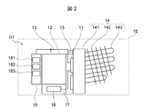
図2は、電力変換装置10の正面構成を示す。電力変換装置10は、パワースイッチング素子11、フィルタコンデンサ12、導体バー13、冷却ユニット14、入出力端子15、ゲート制御回路16、ゲート配線17及び過電圧保護装置18から構成される。
FIG. 2 shows a front configuration of the
電力変換装置10は、単相交流から直流を発生させる装置及び直流から三相交流を発生させる装置である。前者はコンバータと呼ばれ、後者はインバータと呼ばれる。
The
コンバータは、交流電源からの単相交流電圧を直流電圧に変換し、直流電圧平滑用のフィルタコンデンサ12を充電するもので、2相のレグで構成される。
The converter converts a single-phase AC voltage from an AC power source into a DC voltage and charges the DC voltage
インバータは、フィルタコンデンサ12に充電された直流電圧をパワースイッチング素子11のON/OFFの比率を連続的に変化させることで交流電圧に変換するもので、三相のレグで構成される。
The inverter converts the DC voltage charged in the
電力変換装置10は、コンバータ及びインバータを介して三相交流を発生させることにより、鉄道車両Rに設置された電動機を駆動させる。なお何れの電力変換も半導体群を通電制御することで行なわれる。また通電制御に際して、別に設けられている制御装置は、制御信号を出力し、電力変換装置10に取付けられたゲート制御回路16及びゲート配線17を介して、パワースイッチング素子11を駆動する。
The
パワースイッチング素子11は、例えばIGBT(Insulated Gate Bipolar Transistor)である。IGBTは、ON抵抗及び駆動電流が小さく、またスイッチング速度が速いという利点がある。一方で、通電及び遮断時に大電力を消費して発熱するため、本実施の形態においては放熱のために冷却ユニット14が設けられる。
The
フィルタコンデンサ12は、上述したように直流電圧を平滑するためのものである。
導体バー13は、外部機器と電気的に接続するための平板状の接続線であり、ラミネートブスバーとも呼ばれる。ラミネートブスバーは、IGBTなどのパワースイッチング素子11を用いた電気回路において高速スイッチング時に生じる異常電圧(サージ電圧)を抑制させる構造を有する。
The
The
具体的に導体バー13は、導体の発熱を抑えるため、材料としては体積抵抗率の小さい銅が用いられ、また導体断面積が大きい形状を有する。導体バー13を薄い平板形状とした理由は、配線インダクタンスを低減させるためである。
Specifically, the
冷却ユニット14は、冷却ブロック141、冷却フィン142及びヒートパイプ143から構成される。冷却ブロック141は、パワースイッチング素子11から発生した熱を吸収し、ヒートパイプ143に封入された冷媒を気化して冷却する。冷却フィン142は、気化した冷媒を風に当てて熱交換することにより冷媒を再び液化させる。なお本実施の形態における冷却ユニット14は、ヒートパイプ式が採用されているがこれに限らず、ラジエータ式を採用してもよい。
The
入出力端子15は、直流を入力するための直流端子P及びNと、直流端子P及びNから入力された直流を任意周波数及び任意電圧の3相交流に変換して出力するための交流端子U、V及びWから構成される。
The input /
ゲート制御回路16は、ゲート信号を生成及び出力するための回路である。ゲート配線17は、ゲート制御回路16から生成及び出力されたゲート信号をパワースイッチング素子11に出力するための配線である。
The
過電圧保護装置18は、直流電圧検出器181、パワースイッチング素子182及び駆動回路183から構成される。過電圧保護装置18は、フィルタコンデンサ12の過電圧検出時や制御電源OFF時にパワースイッチング素子182をONし、フィルタコンデンサ12に蓄積されている電荷を放出させるための装置である。直流電圧検出器181は、フィルタコンデンサ12の過電圧を検出し、パワースイッチング素子182は、フィルタコンデンサ12に蓄積されている電荷を放出する際にONに切り替えられ、駆動回路183は、パワースイッチング素子182を駆動してON/OFFを切り替える。
The
なお従来の過電圧保護装置は、上述の構成に加えて、スナバ回路を備えて構成される。スナバ回路は、パワースイッチング素子182のOFF時に発生するサージ電圧を抑制するため、配線のインダクタンス成分に蓄えられたエネルギーをスナバコンデンサに転流させる回路であり、スナバ抵抗器、スナバダイオード及びスナバコンデンサから構成される。
The conventional overvoltage protection device includes a snubber circuit in addition to the above-described configuration. The snubber circuit is a circuit that commutates the energy stored in the inductance component of the wiring to the snubber capacitor in order to suppress the surge voltage generated when the
本実施の形態においては、従来の過電圧保護装置からスナバ回路を廃止した過電圧保護装置18を採用して、軽量化及び小型化を実現しようとするものである。
In the present embodiment, the
ここで、上述したようにスナバ回路はサージ電圧を抑制するための回路であるから、スナバ回路を廃止するとサージ電圧の抑制が困難になるところ、本実施の形態においては過電圧保護装置18をフィルタコンデンサ12に近接して配置し、過電圧保護装置18とフィルタコンデンサ12との間の配線(導体バー13)の長さが可能な限り短くなるように構成される。よって配線のインダクタンスが無視できるレベルとなるため、サージ電圧の発生を抑制することができる。
Here, since the snubber circuit is a circuit for suppressing the surge voltage as described above, it becomes difficult to suppress the surge voltage if the snubber circuit is abolished. In the present embodiment, the
図3は、電力変換装置10の斜視構成を示す。図3に示す斜視構成は、図2に示す方向D1から見た斜視構成である。電力変換装置10は、手前側から奥側にかけて、過電圧保護装置18、フィルタコンデンサ12、冷却ブロック141及び冷却フィン142が順に配置され、冷却ブロック141には入出力端子15が設けられて構成される。これらは、電力変換装置10として同一筐体1内に収納される。
FIG. 3 shows a perspective configuration of the
図4は、電力変換装置10の要部正面構成を示す。ここでは図2に示した電力変換装置10のうち、特にパワースイッチング素子11、フィルタコンデンサ12、導体バー13、冷却ブロック141及び過電圧保護装置18を示す。
FIG. 4 shows a front view of a main part of the
フィルタコンデンサ12及び過電圧保護装置18は、それぞれに設けられた端子が同一方向となるように配置され、かつ、互いに近接して配置される。導体バー13は、これらフィルタコンデンサ12及び過電圧保護装置18の上面に沿って延在して設置され、またパワースイッチング素子11、フィルタコンデンサ12及び過電圧保護装置18をそれぞれ接続するように設置される。
The
本実施の形態においては、フィルタコンデンサ12と過電圧保護装置18との間の物理的な距離L1及びL2が可能な限り短くなるような配置構成を採用したので、過電圧保護装置18からスナバ回路を廃止しても、この部分に誘導電圧が発生することを抑制することができる。
In the present embodiment, an arrangement configuration is adopted in which the physical distances L1 and L2 between the
図5は、電力変換装置10の回路構成を示す。鉄道のき電方式には、交流式及び直流式があり、電動機にも交流電動機及び直流電動機とが存在する。よってき電方式と電動機との組み合わせにより電力変換装置10にもインバータ単独、コンバータ単独又は両者の組み合わせが有り得る。本実施の形態においては、一例として直流き電方式と交流電動機との組み合わせの場合に適用するインバータについて説明する。
FIG. 5 shows a circuit configuration of the
本実施の形態における電力変換装置10の主回路は、入出力端子15のうちの直流端子P及びN間に接続されるフィルタコンデンサ12と、3相インバータとによって構成される。3相インバータは、入力された直流を任意周波数及び任意電圧の3相交流に変換し、入出力端子15のうちの交流端子U、V、Wに3相交流を出力するものである。
The main circuit of
3相インバータは、6つのパワースイッチング素子11から構成される。各相のパワースイッチング素子11は、素子と素子に並列接続されたフリーホイールダイオードとから構成される。
The three-phase inverter is composed of six
本実施の形態においては、フィルタコンデンサ12と過電圧保護装置18との間の配線の長さL1及びL2を可能な限り短くするようにしたので、このL1及びL2部分に誘導電圧が発生することを抑制することができる。
In the present embodiment, the lengths L1 and L2 of the wiring between the
以下図6〜図8を参照して、従来の電力変換装置10Aについて説明する。本実施の形態における電力変換装置10と同様の構成については同一の符号又は同一の符号にAを付してその説明を省略し、異なる構成について説明する。
Hereinafter, a
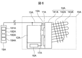
図6は、従来の電力変換装置10Aの正面構成を示す。従来の電力変換装置10Aは、以下の点で本実施の形態における電力変換装置10と異なる。
FIG. 6 shows a front configuration of a
すなわち従来の電力変換装置10Aは、同一筐体1内において過電圧保護装置18Aとは別置きに設置される点、別置きに設置されるため過電圧保護装置18Aとフィルタコンデンサ12Aとの間の配線の長さが一定以上となりこの部分に誘導電圧が発生し、過電圧保護装置18Aに設けられているパワースイッチング素子182Aに誘導電圧が印加するおそれがある点、パワースイッチング素子182Aを保護するために過電圧保護装置18A内にスナバ回路184Aが設けられる点で、本実施の形態における電力変換装置10と異なる。
That is, the conventional
図7は、従来の電力変換装置10Aの斜視構成を示す。電力変換装置10Aは、手前側から奥側にかけて、フィルタコンデンサ12A、冷却ブロック141A及び冷却フィン142Aが順に配置され、フィルタコンデンサ12Aの下部にはゲート制御回路16Aが設置され、冷却ブロック141には入出力端子15Aが設けられて構成される。これらは、電力変換装置10Aとして同一筐体1内に収納される。また同一筐体1内において電力変換装置10Aとは別置きに過電圧保護装置18Aが設置される。
FIG. 7 shows a perspective configuration of a
図8は、従来の電力変換装置10Aの要部正面構成を示す。ここでは図6に示した電力変換装置10Aのうち、特にパワースイッチング素子11A、フィルタコンデンサ12A、導体バー13A、冷却ブロック141A及び過電圧保護装置18Aを示す。
FIG. 8 shows a front view of a main part of a
従来の形態においては、フィルタコンデンサ12Aと過電圧保護装置18Aとの間の物理的な距離L11及びL12が長くなるため、この部分に誘導電圧が発生する。よってこの誘導電圧からパワースイッチング素子182Aを保護するため、過電圧保護装置18Aにはスナバ回路184Aが必要となる。スナバ回路184Aは、上述したようにスナバ抵抗器、スナバダイオード及びスナバコンデンサから構成され、特にスナバコンデンサが重くかさ張るものであるため、過電圧保護装置18Aを収納する筐体1の軽量化及び小型化を阻害することになる。
In the conventional configuration, since the physical distances L11 and L12 between the
以上のように本実施の形態によれば、フィルタコンデンサ12と過電圧保護装置18との間の導体配線長が最短となるようにこれらフィルタコンデンサ12及び過電圧保護装置18を近接して配置したので、フィルタコンデンサ12と過電圧保護装置18との間の導体配線のインダクタンス成分を無視できるレベルに減らすことができ、スナバ回路184Aを廃止することができる。よって過電圧保護装置18の軽量化及び小型化を実現することができるとともに、電力変換装置10の信頼性向上を実現することができる。
As described above, according to the present embodiment, the
またフィルタコンデンサ12と過電圧保護装置18との間の接続には、薄型平板形状の導体バー13を近接させて延長して沿わせるようにしたので、更なる配線インダクタンスの低減を図ることができる。
In addition, since the thin flat plate-
また、過電圧保護装置18の軽量化に伴い、過電圧保護装置18を電力変換装置10に直付けし、過電圧保護装置18とフィルタコンデンサ12が近接して配置されるように固定することができる。
Further, as the
1 筐体
10 電力変換装置
11 パワースイッチング素子
12 フィルタコンデンサ
13 導体バー
14 冷却ユニット
15 入出力端子
16 ゲート制御回路
17 ゲート配線
18 過電圧保護装置
DESCRIPTION OF SYMBOLS 1
Claims (4)
直流電圧を平滑化するフィルタコンデンサと、
前記フィルタコンデンサに蓄積されている電荷を放出させる過電圧保護装置と、
直流電圧を交流電圧に変換する複数のパワースイッチング素子と、
前記パワースイッチング素子を冷却する冷却ユニットと、
前記フィルタコンデンサ、前記過電圧保護装置及び前記パワースイッチング素子を電気的に接続する導体バーとを備え、
前記フィルタコンデンサ、前記過電圧保護装置及び前記パワースイッチング素子は、前記電力変換装置の一方側から、前記過電圧保護装置、前記フィルタコンデンサ、前記パワースイッチング素子の順に配置され、
前記過電圧保護装置は、前記フィルタコンデンサに近接して配置され、
前記導体バーに接続される前記フィルタコンデンサの端子及び前記過電圧保護装置の端子は、それぞれ同一側に配置される
ことを特徴とする電力変換装置。 In power converters for railway vehicles,
A filter capacitor for smoothing the DC voltage;
An overvoltage protection device for discharging the charge accumulated in the filter capacitor;
A plurality of power switching elements for converting a DC voltage into an AC voltage;
A cooling unit for cooling the power switching element;
A conductor bar that electrically connects the filter capacitor, the overvoltage protection device, and the power switching element;
The filter capacitor, the overvoltage protection device, and the power switching element are arranged in order of the overvoltage protection device, the filter capacitor, and the power switching element from one side of the power conversion device,
The overvoltage protection device is disposed in proximity to the filter capacitor ;
The power converter according to claim 1, wherein a terminal of the filter capacitor and a terminal of the overvoltage protection device connected to the conductor bar are arranged on the same side .
前記電力変換装置に直付けにより固定される
ことを特徴とする請求項1に記載の電力変換装置。 The overvoltage protection device is:
Power converter according to claim 1, characterized in that it is fixed by directly attached to the power converter.
前記フィルタコンデンサに蓄積される電圧を検出する直流電圧検出器と、
前記フィルタコンデンサに蓄積されている電荷を放出する際にONに切り替えられる過電圧保護装置用パワースイッチング素子と、
前記過電圧保護装置用パワースイッチング素子の駆動を制御する駆動回路とを備えて構成される
ことを特徴とする請求項1又は2に記載の電力変換装置。 The overvoltage protection device is:
A DC voltage detector for detecting the voltage accumulated in the filter capacitor;
A power switching element for an overvoltage protection device that is switched on when discharging the charge accumulated in the filter capacitor;
Power converter according to claim 1 or 2, characterized in that formed and a driver circuit for controlling the driving of the overvoltage protection device for a power switching element.
薄型かつ平板形状を有し、前記フィルタコンデンサと、前記過電圧保護装置との間に跨って延在して配置され、前記フィルタコンデンサと前記過電圧保護装置とを接続する
ことを特徴とする請求項1〜3の何れか一項に記載の電力変換装置。 The conductor bar is
2. The thin and flat plate shape is disposed so as to extend between the filter capacitor and the overvoltage protection device, and connects the filter capacitor and the overvoltage protection device. The power conversion device according to any one of to 3 .
Priority Applications (4)
| Application Number | Priority Date | Filing Date | Title |
|---|---|---|---|
| JP2013176323A JP6182021B2 (en) | 2013-08-28 | 2013-08-28 | Power converter |
| EP14179244.0A EP2842791B1 (en) | 2013-08-28 | 2014-07-31 | Power converter |
| KR1020140098989A KR101600186B1 (en) | 2013-08-28 | 2014-08-01 | Power converter |
| CN201410377271.9A CN104426385B (en) | 2013-08-28 | 2014-08-01 | Power-converting device |
Applications Claiming Priority (1)
| Application Number | Priority Date | Filing Date | Title |
|---|---|---|---|
| JP2013176323A JP6182021B2 (en) | 2013-08-28 | 2013-08-28 | Power converter |
Publications (2)
| Publication Number | Publication Date |
|---|---|
| JP2015046993A JP2015046993A (en) | 2015-03-12 |
| JP6182021B2 true JP6182021B2 (en) | 2017-08-16 |
Family
ID=51229841
Family Applications (1)
| Application Number | Title | Priority Date | Filing Date |
|---|---|---|---|
| JP2013176323A Active JP6182021B2 (en) | 2013-08-28 | 2013-08-28 | Power converter |
Country Status (4)
| Country | Link |
|---|---|
| EP (1) | EP2842791B1 (en) |
| JP (1) | JP6182021B2 (en) |
| KR (1) | KR101600186B1 (en) |
| CN (1) | CN104426385B (en) |
Cited By (1)
| Publication number | Priority date | Publication date | Assignee | Title |
|---|---|---|---|---|
| JP7025065B2 (en) | 2017-11-02 | 2022-02-24 | ピン マーケティング エセエレ | Equipment and methods for arranging at least one bowling pin |
Families Citing this family (5)
| Publication number | Priority date | Publication date | Assignee | Title |
|---|---|---|---|---|
| JP5778840B1 (en) * | 2014-09-25 | 2015-09-16 | 株式会社日立製作所 | Power conversion unit and power conversion device |
| JP6429720B2 (en) * | 2015-05-07 | 2018-11-28 | 株式会社日立製作所 | Power converter and railway vehicle |
| JP6429721B2 (en) * | 2015-05-07 | 2018-11-28 | 株式会社日立製作所 | Power converter and railway vehicle |
| JP6529868B2 (en) * | 2015-09-09 | 2019-06-12 | 株式会社東芝 | Electric car control device |
| DE112019007151T5 (en) | 2019-04-01 | 2021-12-09 | Mitsubishi Electric Corporation | POWER CONVERTER DEVICE |
Family Cites Families (15)
| Publication number | Priority date | Publication date | Assignee | Title |
|---|---|---|---|---|
| JPS583957A (en) | 1981-06-27 | 1983-01-10 | Nisshin Steel Co Ltd | Zinc hot dipping device |
| JPS60200703A (en) * | 1984-03-26 | 1985-10-11 | Hitachi Ltd | Controller of ac electric railcar |
| JPH0583957A (en) * | 1991-09-18 | 1993-04-02 | Hitachi Ltd | Power converter |
| JPH0937414A (en) * | 1995-07-20 | 1997-02-07 | Mitsubishi Electric Corp | Inverter on-board electric car |
| JP3263316B2 (en) * | 1996-06-28 | 2002-03-04 | 株式会社日立製作所 | Electric vehicle control device |
| JPH1098887A (en) * | 1996-09-20 | 1998-04-14 | Hitachi Ltd | Power converter |
| US6160696A (en) * | 1998-05-04 | 2000-12-12 | General Electric Company | Modular bus bar and switch assembly for traction inverter |
| JP3046276B2 (en) * | 1998-05-11 | 2000-05-29 | 三菱電機株式会社 | Power converter |
| KR100485102B1 (en) * | 2002-09-17 | 2005-04-20 | 주식회사 플라스포 | Inverter stack having multi-layer bus plate |
| JP4356434B2 (en) * | 2003-11-27 | 2009-11-04 | 富士電機システムズ株式会社 | 3-level inverter circuit |
| JPWO2008001427A1 (en) * | 2006-06-27 | 2009-11-19 | 三菱電機株式会社 | Power converter |
| JP5367444B2 (en) * | 2009-04-28 | 2013-12-11 | 株式会社東芝 | Electric vehicle control device and test method thereof |
| BR112012014205A2 (en) * | 2009-12-18 | 2016-06-14 | Mitsubishi Electric Corp | drive control device for an electric train |
| SG184129A1 (en) * | 2010-03-31 | 2012-10-30 | Toshiba Kk | Electric-vehicle control apparatus |
| EP2506421B1 (en) * | 2011-03-31 | 2020-07-08 | Kabushiki Kaisha Toshiba | Electric vehicle control device |
-
2013
- 2013-08-28 JP JP2013176323A patent/JP6182021B2/en active Active
-
2014
- 2014-07-31 EP EP14179244.0A patent/EP2842791B1/en active Active
- 2014-08-01 CN CN201410377271.9A patent/CN104426385B/en active Active
- 2014-08-01 KR KR1020140098989A patent/KR101600186B1/en active IP Right Grant
Cited By (1)
| Publication number | Priority date | Publication date | Assignee | Title |
|---|---|---|---|---|
| JP7025065B2 (en) | 2017-11-02 | 2022-02-24 | ピン マーケティング エセエレ | Equipment and methods for arranging at least one bowling pin |
Also Published As
| Publication number | Publication date |
|---|---|
| EP2842791A2 (en) | 2015-03-04 |
| JP2015046993A (en) | 2015-03-12 |
| EP2842791A3 (en) | 2015-09-16 |
| KR20150026810A (en) | 2015-03-11 |
| CN104426385A (en) | 2015-03-18 |
| KR101600186B1 (en) | 2016-03-04 |
| CN104426385B (en) | 2017-10-03 |
| EP2842791B1 (en) | 2021-08-25 |
Similar Documents
| Publication | Publication Date | Title |
|---|---|---|
| JP6182021B2 (en) | Power converter | |
| JP6373702B2 (en) | Semiconductor power module and semiconductor drive device | |
| WO2014010061A1 (en) | Control board for on-board motor drive | |
| JP2009005462A (en) | Power conversion device | |
| JP6812317B2 (en) | Vehicles equipped with power converters and power converters | |
| JPWO2019026339A1 (en) | Power converter and vehicle equipped with the power converter | |
| JP2009105178A (en) | Power semiconductor unit | |
| JP2010245910A (en) | Electric power conversion apparatus and on-vehicle electric system using the same | |
| JP2013162690A (en) | Vvvf inverter and vehicle controller | |
| JP2008514181A (en) | Power converter | |
| JP2006197735A (en) | Inverter | |
| CN103813929B (en) | There is the drive system of the battery operation vehicle of the permanent excited synchronous motor of being powered by current converter | |
| TWI590570B (en) | Power conversion device and vehicle control device | |
| JP6243320B2 (en) | Power semiconductor module | |
| JP2015033222A (en) | Drive unit of semiconductor device and power conversion device using the same | |
| JP5742762B2 (en) | Power converter | |
| JP4735109B2 (en) | Matrix converter device | |
| JP5841678B2 (en) | Inverter and power system with fuse protection | |
| JP6713246B2 (en) | Power converter | |
| JP5058545B2 (en) | Electric vehicle control device | |
| JP2017169344A (en) | Power conversion device | |
| JP2005094882A (en) | Power module | |
| JP4424918B2 (en) | Power converter | |
| JP6906431B2 (en) | Flow reducer | |
| JP2017108521A (en) | Electric power conversion device |
Legal Events
| Date | Code | Title | Description |
|---|---|---|---|
| A621 | Written request for application examination |
Free format text: JAPANESE INTERMEDIATE CODE: A621 Effective date: 20160212 |
|
| A977 | Report on retrieval |
Free format text: JAPANESE INTERMEDIATE CODE: A971007 Effective date: 20161227 |
|
| A131 | Notification of reasons for refusal |
Free format text: JAPANESE INTERMEDIATE CODE: A131 Effective date: 20170105 |
|
| A521 | Request for written amendment filed |
Free format text: JAPANESE INTERMEDIATE CODE: A523 Effective date: 20170303 |
|
| TRDD | Decision of grant or rejection written | ||
| A01 | Written decision to grant a patent or to grant a registration (utility model) |
Free format text: JAPANESE INTERMEDIATE CODE: A01 Effective date: 20170711 |
|
| A61 | First payment of annual fees (during grant procedure) |
Free format text: JAPANESE INTERMEDIATE CODE: A61 Effective date: 20170721 |
|
| R150 | Certificate of patent or registration of utility model |
Ref document number: 6182021 Country of ref document: JP Free format text: JAPANESE INTERMEDIATE CODE: R150 |