JP6179552B2 - Method for manufacturing coated film conductor - Google Patents
Method for manufacturing coated film conductor Download PDFInfo
- Publication number
- JP6179552B2 JP6179552B2 JP2015100919A JP2015100919A JP6179552B2 JP 6179552 B2 JP6179552 B2 JP 6179552B2 JP 2015100919 A JP2015100919 A JP 2015100919A JP 2015100919 A JP2015100919 A JP 2015100919A JP 6179552 B2 JP6179552 B2 JP 6179552B2
- Authority
- JP
- Japan
- Prior art keywords
- conducting wire
- conductor
- assembly
- film assembly
- collective
- Prior art date
- Legal status (The legal status is an assumption and is not a legal conclusion. Google has not performed a legal analysis and makes no representation as to the accuracy of the status listed.)
- Expired - Fee Related
Links
Images


Classifications
-
- H—ELECTRICITY
- H01—ELECTRIC ELEMENTS
- H01B—CABLES; CONDUCTORS; INSULATORS; SELECTION OF MATERIALS FOR THEIR CONDUCTIVE, INSULATING OR DIELECTRIC PROPERTIES
- H01B13/00—Apparatus or processes specially adapted for manufacturing conductors or cables
- H01B13/06—Insulating conductors or cables
-
- H—ELECTRICITY
- H02—GENERATION; CONVERSION OR DISTRIBUTION OF ELECTRIC POWER
- H02K—DYNAMO-ELECTRIC MACHINES
- H02K15/00—Processes or apparatus specially adapted for manufacturing, assembling, maintaining or repairing of dynamo-electric machines
- H02K15/10—Applying solid insulation to windings, stators or rotors, e.g. applying insulating tapes
- H02K15/105—Applying solid insulation to windings, stators or rotors, e.g. applying insulating tapes to the windings
-
- H—ELECTRICITY
- H02—GENERATION; CONVERSION OR DISTRIBUTION OF ELECTRIC POWER
- H02K—DYNAMO-ELECTRIC MACHINES
- H02K15/00—Processes or apparatus specially adapted for manufacturing, assembling, maintaining or repairing of dynamo-electric machines
- H02K15/04—Processes or apparatus specially adapted for manufacturing, assembling, maintaining or repairing of dynamo-electric machines of windings prior to their mounting into the machines
- H02K15/0414—Processes or apparatus specially adapted for manufacturing, assembling, maintaining or repairing of dynamo-electric machines of windings prior to their mounting into the machines the windings consisting of separate elements, e.g. bars, segments or half coils
-
- H—ELECTRICITY
- H02—GENERATION; CONVERSION OR DISTRIBUTION OF ELECTRIC POWER
- H02K—DYNAMO-ELECTRIC MACHINES
- H02K15/00—Processes or apparatus specially adapted for manufacturing, assembling, maintaining or repairing of dynamo-electric machines
- H02K15/12—Impregnating, moulding insulation, heating or drying of windings, stators, rotors or machines
-
- H—ELECTRICITY
- H02—GENERATION; CONVERSION OR DISTRIBUTION OF ELECTRIC POWER
- H02K—DYNAMO-ELECTRIC MACHINES
- H02K3/00—Details of windings
- H02K3/04—Windings characterised by the conductor shape, form or construction, e.g. with bar conductors
- H02K3/12—Windings characterised by the conductor shape, form or construction, e.g. with bar conductors arranged in slots
- H02K3/14—Windings characterised by the conductor shape, form or construction, e.g. with bar conductors arranged in slots with transposed conductors, e.g. twisted conductors
-
- H—ELECTRICITY
- H01—ELECTRIC ELEMENTS
- H01B—CABLES; CONDUCTORS; INSULATORS; SELECTION OF MATERIALS FOR THEIR CONDUCTIVE, INSULATING OR DIELECTRIC PROPERTIES
- H01B13/00—Apparatus or processes specially adapted for manufacturing conductors or cables
- H01B13/02—Stranding-up
- H01B13/0292—After-treatment
-
- Y—GENERAL TAGGING OF NEW TECHNOLOGICAL DEVELOPMENTS; GENERAL TAGGING OF CROSS-SECTIONAL TECHNOLOGIES SPANNING OVER SEVERAL SECTIONS OF THE IPC; TECHNICAL SUBJECTS COVERED BY FORMER USPC CROSS-REFERENCE ART COLLECTIONS [XRACs] AND DIGESTS
- Y10—TECHNICAL SUBJECTS COVERED BY FORMER USPC
- Y10T—TECHNICAL SUBJECTS COVERED BY FORMER US CLASSIFICATION
- Y10T29/00—Metal working
- Y10T29/49—Method of mechanical manufacture
- Y10T29/49002—Electrical device making
- Y10T29/49117—Conductor or circuit manufacturing
Landscapes
- Engineering & Computer Science (AREA)
- Power Engineering (AREA)
- Manufacturing & Machinery (AREA)
- Manufacture Of Motors, Generators (AREA)
- Insulated Conductors (AREA)
- Processes Specially Adapted For Manufacturing Cables (AREA)
- Heat Treatment Of Strip Materials And Filament Materials (AREA)
Description
本発明は、被膜集合導線の製造方法に関する。 The present invention relates to a method for manufacturing a film assembly conductor.
電気的な絶縁性を備える絶縁被膜に覆われた被膜集合導線がある。例えば、特許文献1に開示されているように、このような集合導線は、複数の導線を束ねて導線束を形成し、形成した導線束を捻った後で、これを被膜で覆うことによって形成することがある。
There is a film assembly conductor covered with an insulating film having electrical insulation. For example, as disclosed in
ところで、被膜を覆う工程では、集合導線は張力を付与されつつ加熱されることによって、捻れ変形することがあった。 By the way, in the process of covering the film, the assembly conductor may be twisted and deformed by being heated while being applied with tension.
例えば、図21に示すように、束ねた導線束(図示略)を捻じることによって形成される集合導線901がある。集合導線901は、集合導線901の軸を中心に捻られた左巻部901bと、軸方向に真っ直ぐに延びる平行部901aと、左巻部901bと逆方向に捻られた右巻部901cとを備える。集合導線901を被膜で覆う工程等において、捻れ戻り変形が集合導線901に生じる。捻れ戻り変形は、左巻部901bと右巻部901cとが弛緩するように、具体的には、導線束を捻じった回転方向と逆の回転方向902に捻られるように、捻れ変形する。この捻れ変形によって、平行部901aが拡大し、左巻部901b及び右巻部901cが縮小する。
For example, as shown in FIG. 21, there is a collective conducting
このような捻じれ戻り変形が生じると、例えば、図22に示すように、被膜集合導線907の一端部907aが、被膜集合導線907の他端部907cに対して、捻れ変形が生じることがあった。また、図23に示すように、一端部907aの側面907eと、他端部907cの側面907fとが交差して成す捻れ角度αが、被膜集合導線として好ましくない大きさに達することがあった。なお、図22及び図23では、分かり易くするために、被膜集合導線907は1本の導線として図示されている。
When such twist return deformation occurs, for example, as shown in FIG. 22, one
さらに、本出願の発明者等は、上記した被膜集合導線を所定温度になるまで加熱し、所定時間保持するアニール処理を行うことを想起した。このようなアニール処理によって、必要な集合導線と被膜との密着強度を確保する。しかしながら、アニール処理によって、被膜集合導線にさらに捻れ変形が生じてしまうことがあった。 Furthermore, the inventors of the present application recalled that the above-described film assembly conductor was heated to a predetermined temperature and annealed for a predetermined time. By such annealing treatment, necessary adhesion strength between the collective conducting wire and the coating is ensured. However, the annealing treatment may cause further twist deformation in the film assembly conducting wire.
本発明は、捻れ変形を矯正する被膜集合導線の製造方法を提供する。 The present invention provides a method for manufacturing a coated assembly lead that corrects torsional deformation.
本発明にかかる集合導線の製造方法は、
複数の導線を束ねることによって形成される導線束を捻り変形させることによって、右巻部と平行部と左巻部とを有する集合導線を形成する工程と、
前記集合導線を絶縁被膜で被覆することによって被膜集合導線を形成する工程と、
前記被膜集合導線に張力を付与しつつ、前記被膜集合導線をアニール処理温度で加熱保持するアニール処理工程と、
を含む。
The manufacturing method of the collective conducting wire according to the present invention is as follows.
Forming a conducting wire having a right-handed portion, a parallel portion, and a left-handed portion by twisting and deforming a conducting wire bundle formed by bundling a plurality of conducting wires;
Forming a film assembly conductor by coating the assembly conductor with an insulating coating;
An annealing treatment step of heating and holding the coating assembly wire at an annealing temperature while applying tension to the coating assembly wire;
including.
このような構成によれば、集合導線の捻れを抑制しつつ被膜と集合導線との密着強度を高めるので、捻れ変形を矯正して被膜集合導線を製造することができる。 According to such a configuration, the adhesion strength between the coating and the assembly conductor is increased while suppressing the twist of the assembly conductor, so that the twist assembly can be corrected and the coating assembly conductor can be manufactured.
前記被膜集合導線は、前記集合導線を露出させた通電部を両端に有し、
前記アニール処理工程は、前記被膜集合導線をアニール処理温度まで昇温させる加熱工程を含み、
前記加熱工程では、前記被膜集合導線の前記通電部に電流を供給することによって、直接通電加熱を行うことを特徴としてもよい。
The film assembly conducting wire has a current-carrying portion that exposes the assembly conducting wire at both ends,
The annealing treatment step includes a heating step of raising the film assembly conducting wire to an annealing treatment temperature,
In the heating step, direct current heating may be performed by supplying a current to the current-carrying portion of the coated film conductor.
このような構成によれば、被膜集合導線の外部から加熱を行った場合には絶縁被膜が断熱材として作用するため集合導線と絶縁被膜との接触部に熱が伝わりにくいが、被膜集合導線における集合導線の内部にジュール熱を発生させることによって、被膜集合導線をアニール処理温度まで短時間で昇温させる。したがって、良好な生産性で、捻れ変形を矯正して被膜集合導線を製造することができる。 According to such a configuration, when the coating collective conductor is heated from the outside, the insulating coating acts as a heat insulating material, so that heat is not easily transmitted to the contact portion between the collective conducting wire and the insulating coating. By generating Joule heat inside the collective conducting wire, the temperature of the coating collective conducting wire is raised to the annealing temperature in a short time. Therefore, it is possible to manufacture the film assembly lead wire by correcting torsional deformation with good productivity.
また、前記アニール処理工程では、前記被膜集合導線に対して、前記被膜集合導線の形成工程において発生した捻れ戻り変形による捻れの角度が実質的にゼロとなるように前記被膜集合導線の両端部が固定された状態で、前記被膜集合導線に張力を付与することを特徴としてもよい。 Further, in the annealing treatment step, both end portions of the coating assembly conductor are set to be substantially zero with respect to the coating assembly conductor so that the twist angle due to the twist return deformation generated in the coating assembly formation process is substantially zero. A tension may be applied to the film assembly conducting wire in a fixed state.
このような構成によれば、被膜集合導線の捻れをさらに抑制しつつ張力を付与するので、より確実に捻れ変形を矯正して被膜集合導線を製造することができる。 According to such a configuration, since the tension is applied while further suppressing the twist of the coated film conductor, the twisted deformation can be more reliably corrected and the coated film conductor can be manufactured.
また、前記アニール処理工程の前において、
前記被膜集合導線を切断することによって、短尺化する工程をさらに含む
ことを特徴としてもよい。
In addition, before the annealing step,
It may be characterized by further comprising a step of shortening by cutting the coated film conducting wire.
このような構成によれば、被膜集合導線が短尺化されることによって被膜集合導線の取り回しが容易になる。これによって、短尺化された被膜集合導線毎に加熱処理を行うことができるため、加熱装置等を小型化できる。また、短尺化された被膜集合導線に対して個別に張力を付与するため、付与する張力を小さくすることができることから張力を付与する装置を小型化できる。 According to such a configuration, the film assembly conductor is shortened, thereby facilitating the handling of the film assembly conductor. Thereby, since the heat treatment can be performed for each of the shortened coated film conductors, the heating device and the like can be downsized. Moreover, since tension | tensile_strength is individually provided with respect to the shortened film assembly conducting wire, since the tension | tensile_strength to apply can be made small, the apparatus which provides tension | tensile_strength can be reduced in size.
本発明によれば、捻れ変形を矯正する被膜集合導線の製造方法を提供することができる。 ADVANTAGE OF THE INVENTION According to this invention, the manufacturing method of the film assembly conducting wire which corrects a twist deformation can be provided.
実施の形態1.
図1〜図14を参照して実施の形態1にかかる被膜集合導線の製造方法について説明する。図1は、実施の形態1にかかる被膜集合導線の製造方法を示すフローチャートである。図2は、実施の形態1にかかる被膜集合導線の製造方法の複数の工程を示す模式図である。まず、製造装置140を用いて、導体線群198から集合導体202を連続的に製造する複数の工程について説明する。図1中、導体線群198は、導体線109が紙面の奥から手前の方向(ここではY方向)に並んだ状態を模式的に表している。
With reference to FIGS. 1-14, the manufacturing method of the film assembly conducting
図2に示すように、素線供給機141は導体線群198を第1圧延ロール142に送る。模式図161に示すように、導体線109は略円形状の断面形状を有する線状体である。導体線109は、周辺素線110を形成する導体線群198の一部である。導体線109は、電気を伝導する材料、例えば、純銅又は銅合金からなる。
As shown in FIG. 2, the
第1圧延ロール142は導体線群198を素線供給機141から受けて、模式図162に示すように導体線群198の導体線109を塑性変形させて、周辺素線110を形成する(単線圧延工程S1)。ここで、周辺素線110の断面形状は、断面形状が回転により変化しない等方性を有する円形状から、断面形状が回転により変化する異方性を有する異方性断面形状に変形すればよく、例えば、上底と下底の長さの異なる台形状に変形する。異方性断面形状として、例えば、台形状、扇形状、円弧状、三角形状などが挙げられる。また、周辺素線110及び中心素線130からなる素線群199内の各素線は、直列に配置されている。即ち素線群199の各素線は、当該素線群199の送り出し方向(素線群199に含まれる各素線の長手方向(ここではX方向))に対して垂直な方向(ここではY方向)に一列に並んで配置されている。より具体的には、周辺素線110において、台形状の上底に相当する面と、台形状の下底に相当する面とが互いに交互に配置されるように配置されている。
The
第1圧延ロール142は、1対のロールを有し、図示しない駆動機構により回転し、素線群199を、搬送装置144に送る。かかる素線群199は、各素線が紙面の奥から手前の方向に一列に並んだ状態を模式的に表している。
The
搬送装置144は、素線群199を第1圧延ロール142から受ける。搬送装置144は、素線群199の各素線を展開し、周辺素線110が中心素線130を取り囲む位置関係を作る。より具体的には、模式図163に示すように、周辺素線110が中心素線130を中心として放射状に配置される(展開工程S2)。このとき、各周辺素線110は、外周面が内周面よりも面積が広くなるように配置される。即ち、各周辺素線110の断面において、台形状の上底又は下底のうち長さの長い方が外側に、短い方が内側に位置するように配置される。
The
また、搬送装置144は、周辺素線110の内周面が中心素線130の各辺に向くように周辺素線110の位置及び向きを整える。即ち、周辺素線110の内周面は、円柱状の中心素線130の外周面に沿う必要があるから、各周辺素線110の上底を含む面と下底を含む面が平行になるようにして搬送された素線群199が、中心素線130から外側に放射状に延びる仮想線に対して垂直になるように角度を変換して配置される必要がある。搬送装置144は、素線群199をクランプ145に送る。
Further, the
続いて、クランプ145は、素線群199を搬送装置144から受ける。クランプ145は、素線群199を整列して、中心素線130の周囲に周辺素線110を配置し、束ねた集合導線、すなわち、集合導線束200を形成する(束形成工程S3)。また、クランプ145は、周辺素線110の内周面が中心素線130の外表面の各辺と対向するように、集合導線束200を形成する。
Subsequently, the
クランプ145は、集合導線束200の中心方向に向かって、所定の圧力を集合導線束200に加える。このため、模式図164に示すように、集合導線束200の断面190において、中心素線130及び周辺素線110並びに周辺素線110同士は接近する。集合導線束200を、クランプ145及び回転機146を通過させて、さらにクランプ147まで送る。
The
クランプ145、回転機146及びクランプ147が集合導線束200をクランプし、集合導線束200の軸を固定する。さらに、クランプ145、回転機146及びクランプ147が集合導線束200をクランプしたまま、回転機146が所定の回転方向150に回転し、集合導線束200を捻る(捻り工程S4)。すると、捻れ集合導体201が形成される。ここで、捻れ集合導体201は、例えば、回転機146を境に、中心素線130を軸として螺旋を描くように捻じれている捻じれ部分と、この捻じれ部分の捻じれ方向と逆方向に捻じれている逆捻じれ部分とを有する。なお、捻れ集合導体201は、捻じれ部分と逆捻じれ部分との間には、中心素線130の軸と平行となる非捻じれ部分を有してもよい。具体的には、図3に示すように、捻れ集合導体201は、平行部201aと、左巻部201bと、右巻部201cとを有する。図3は、実施の形態1にかかる被膜集合導線の製造方法の一工程における集合導線の模式図である。平行部201aと、左巻部201bと、右巻部201cとは、捻れ集合導体201の進行方向(ここで、X方向)に、左巻部201b、平行部201a、右巻部201c、平行部201aとの順に配置されている。捻り工程S4を1回行うと、平行部201a、左巻部201b、平行部201a、及び、右巻部201c、平行部201aが形成される。ここでは、平行部201a、左巻部201b、平行部201a、右巻部201c、及び、平行部201aを1P(ピッチ)とした。
The
図2中の模式図165に示すように、捻れ集合導体201は中心素線130及び所定の形状を有する周辺素線110を整列した集合導体である。このため、回転機146は、断面190の実質的な円形状が維持された断面191を形成することができる。
As shown in a schematic diagram 165 in FIG. 2, the twisted
クランプ147は、捻れ集合導体201の中心方向に向かって、所定の圧力を捻れ集合導体201に加える。このため、中心素線130及び周辺素線110並びに周辺素線110同士を密着させる。
The
第2圧延ロール151は、捻れ集合導体201をクランプ147から受ける。第2圧延ロール151は、1対のロールを有し、図示しない駆動機構により回転し、捻れ集合導体201を実質的な平角形状とした場合の図2中の縦方向(ここで、Z軸方向)に、実質的に圧力をかける。さらに、第3圧延ロール152は、模式図167に示すように、集合導体202の断面192の図2中の上下端に横方向(ここで、Y軸方向)に沿う外壁面194を形成させる(仕上げ圧延工程S5)。なお、必要に応じて、少なくとも1対の圧延ロールを用いて、図2中の左右端に縦方向(ここで、Z軸方向)に沿う壁面を形成してもよい。集合導体202は、中心素線132及び周辺素線112を有する。
The
続いて、図4に示すように、酸化炉153は、第3圧延ロール152(図2参照)から集合導体202を受ける。図4は、実施の形態1にかかる被膜集合導線の製造方法の複数の工程を示す模式図である。集合導体202を内部酸化温度まで加熱することで、集合導体202の内側、すなわち、中心素線132(図2参照)と周辺素線112(図2参照)との間、周辺素線112同士の間に酸化膜を形成する(内部酸化工程S6)。集合導体202は、酸化炉153内で巻付ロール153aに巻き付けられる。この酸化膜は、中心素線132と周辺素線112とを電気的に絶縁し、周辺素線112同士を電気的に絶縁すると好ましい。また、内部酸化工程S6の前において、酸化膜を形成する酸化膜形成剤を塗布しておくとよい。
Subsequently, as shown in FIG. 4, the
続いて、絶縁被膜204aを集合導体203に被覆し、外側被膜集合導線204を形成する(外部被膜形成工程S7)。具体的には、絶縁被膜付与装置154は集合導体203を受ける。集合導体203は引抜ダイ154aのダイス孔154bに導かれる。絶縁被膜付与装置154は、予め、ホッパー154cに装填された粉末状の原料154dを加熱により軟化させており、スクリュー154eにより引抜ダイ154aのダイス孔154bへ射出してさらに加圧する。その後、集合導体203を引抜ダイ154aのダイス孔154bから下流側に引き抜く。すると、絶縁被膜204aが集合導体203の外周面に形成された状態で、外側被膜集合導線204が引抜ダイ154aのダイス孔154bから引き抜かれる。以上の工程により、外側被膜集合導線204が製造される。
Subsequently, the insulating
ここで、絶縁被膜204aは、電気的に絶縁する性質を有する材料からなるとよい。このような材料として、例えば、PFA(テトラフルオロエチレン・パーフルオロアルキルビニルエーテル共重合体)、PEEK(ポリエーテルエーテルケトン)、PPS(ポリフェニレンサルファイド)、エナメルが挙げられる。なお、外側被膜集合導線204は、外部被膜形成工程S7において、加熱や張力を与えられることによって、捻れ戻り変形や捻れ変形が生じることがある。
Here, the insulating
続いて、外側被膜集合導線204を所定の温度まで冷却する(冷却工程S8)。具体的には、まず、冷却装置155が外側被膜集合導線204を受ける。冷却装置155は、冷却水を保持する水槽155aと、水槽155aに設けられる一対のロール155bとを有する。冷却装置155は、外側被膜集合導線204を一対のロール155bの間を通過させる。これによって、外側被膜集合導線204を水槽155a内に浸して、冷却することができる。
Subsequently, the outer coating
続いて、外側被膜集合導線204に圧力をかけて、外側被膜集合導線204の真直度を高める(真直出し工程S9)。具体的には、外側被膜集合導線204をその軸に関して実質的に垂直な方向に並ぶ1対のロール156a、156bに送る。1対のロール156a、156bがそれぞれ、外側被膜集合導線204に圧力をかける。この圧力をかける方向は、外側被膜集合導線204の軸に関して実質的に垂直な方向である。1対のロール156aの並ぶ方向と、1対のロール156bの並ぶ方向とは、実質的に垂直であってもよい。
Subsequently, pressure is applied to the outer coating
図5及び図6に示すように、プレス機157を用いて、外側被膜集合導線204を切断する(切断工程S10)。図5〜図8は、実施の形態1にかかる被膜集合導線の製造方法の一工程を示す模式図である。具体的には、ダイ157bを外側被膜集合導線204の下側に設けて、外側被膜集合導線204の上方からパンチ157aを降下させることによって、外側被膜集合導線204を切断して、短尺化させる。これによって、短尺集合導線205を形成する。短尺集合導線205の長さは、本製造方法の完成品である被膜集合導線の利用用途に応じて決定するとよく、例えば、被膜集合導線の利用用途がモータのショートコイル(後述)である場合、ショートコイルの長さに応じて決定するとよい。また、短尺集合導線205の長さは、アニール炉40(後述)やクランプユニット20(後述)等の製造装置のサイズに応じて決定してもよい。
As shown in FIG.5 and FIG.6, the outer side film | membrane
図7に示すように、円盤状カッタ158を用いて、短尺集合導線205の外側被膜205aの両端部を切断する(プレカット工程S11)。なお、外側被膜205aの両端部を切断する一方で、短尺集合導線205の導線(図示略)を切断しないため、短尺集合導線205の導線(図示略)は損傷しない。
As shown in FIG. 7, both ends of the
続いて、図8に示すように、刃159を用いて、外側被膜205aの両端部を剥離し、部分被膜集合導線206を形成する(剥離工程S12)。具体的には、刃159を外側被膜205aに挿入し、短尺集合導線205の端側に向かって移動させることによって、切断した外側被膜205aの両端部を剥離する。部分被膜集合導線206は、絶縁被膜206aと、絶縁被膜206aに覆われている集合導線206bとを備える。集合導線206bの少なくとも中央部は、絶縁被膜206aに覆われており、電気的に絶縁されている。集合導線206bの両端部(通電部と称してもよい。)は、絶縁被膜206aに覆われておらず露出した状態であり、通電可能である。
Subsequently, as shown in FIG. 8, both ends of the
続いて、部分被膜集合導線206に張力を付与しつつ、アニール処理温度に達するまで加熱して、所定時間保持する(アニール処理工程S13)。
Subsequently, while applying tension to the partial coating
具体的には、図9を参照しつつ図10〜図12に示すように、部分被膜集合導線206をクランプユニット20にクランプさせた状態で、部分被膜集合導線206をクランプユニット20ごとアニール炉40に入れて、所定の温度で加熱して、所定時間保持する。図9は、実施の形態1にかかる被膜集合導線の製造方法の一工程を示すフローチャートである。図10は、実施の形態1にかかる被膜集合導線の製造方法で用いたクランプユニットの斜視図である。図11は、実施の形態1にかかる被膜集合導線の製造方法で用いたクランプユニットの正面図である。図12は、実施の形態1にかかる被膜集合導線の製造方法の一工程を示す模式図である。
Specifically, as shown in FIGS. 10 to 12 with reference to FIG. 9, the partial
図10及び図11に示すように、クランプユニット20は、ベース21と、クランプ支持部22と、クランプ23と、バネ支持部24と、ロッド25と、クランプ支持部26と、クランプ27とを含む。ベース21は、長方形板状体であり、クランプ支持部22は、ベース21の一端に設けられるブロック状体である。バネ支持部24は、ベース21の他端部側に設けられるブロック状体である。ロッド25は、バネ支持部24にバネ(図示略)を介して摺動可能に挿入される。クランプ支持部26はロッド25におけるベース21の他端側に接続されて、ベース21の他端上を移動可能に設けられる。クランプ27は、クランプ支持部26に支持される。
As shown in FIGS. 10 and 11, the
クランプ23とクランプ27とは同じ仮想軸V1上に配置されており、対向している。クランプ支持部26が移動するとき、クランプ27は仮想軸V1上を移動する。仮想軸V1は、ベース21の長手方向に関して実質的に平行であるとよい。クランプ23とクランプ27とは、具体的には、部分被膜集合導線206を締め付けることによって所定位置に固定する固定具であり、例えば、チャック装置である。
The
まず、クランプユニット20を用いて、部分被膜集合導線206に張力を付与する(クランプ工程S131)。具体的には、クランプ23が部分被膜集合導線206の一端部をクランプしつつ、クランプ27が部分被膜集合導線206の他端部をクランプすることで、クランプユニット20は部分被膜集合導線206をクランプすることができる。ここで、バネの復元力によってロッド25及びクランプ支持部26が押されて、クランプ27がクランプ23から離れる方向に押される。そのため、部分被膜集合導線206を、少なくとも仮想軸V1上に真っ直ぐに延ばすように張力をかける。部分被膜集合導線206の他端部は、部分被膜集合導線206の一端部に対して、外部被膜形成工程S7等において生じ得る捻れ戻り変形や捩れ変形を矯正するように、捻れないようにするとよい。ここで、「捻れないようにする」を言い換えると、捻れ角度、つまり、部分被膜集合導線206の他端部の、部分被膜集合導線206の一端部に対する角度が実質的に0(ゼロ)°であると好ましい。
First, tension is applied to the partial film
続いて、部分被膜集合導線206を加熱保持することによって、アニール処理を行う(炉加熱保持工程S132)。なお、アニール処理は、焼きなまし処理に限らず一般的な加熱処理を含む。具体的には、図12に示すように、部分被膜集合導線206をクランプしたクランプユニット20を、アニール炉40の内側に配置されたコンベア10に載せる。部分被膜集合導線206の軸をコンベア10の幅方向に沿うように配置したクランプユニット20の複数を、コンベア10の移動方向に並べるとよい。部分被膜集合導線206は並列して配置される。アニール炉40は、例えば、赤外線を放射させたり、熱風を発生させたりすることによって、アニール炉40の炉室(図示略)内に配置された被加熱物を加熱することができる。アニール炉40によって、部分被膜集合導線206をアニール処理温度になるまで加熱した後、アニール処理温度を保持しつつ、コンベア10は、回転ロール11、12を同じ方向に回転させて、ベルト13を移動させる。これによって、複数のクランプユニット20をアニール炉40を通過させて、複数の部分被膜集合導線206に連続的にアニール処理を施すことができる。切断工程S10によって短尺化した部分被膜集合導線を並列配置させるため、コンベア10の移動方向においてコンパクトな全長のアニール炉を用いて、アニール処理を行うことができる。また、アニール処理によって、絶縁被膜206aと集合導線206bとの密着強度が高められる。
ここで、部分被膜集合導線206は外側被膜集合導線204(図4〜6参照)と比較して短尺であるため、その取り回しが容易になる。これによって、部分被膜集合導線206毎に加熱処理を行うことができるため、アニール炉40等の加熱装置等を小型化できる。また、部分被膜集合導線206に対して個別に張力を付与するため、付与する張力を小さくすることができる。そのため、張力を付与する装置、例えば、クランプユニット20を小型化できる。
Subsequently, annealing is performed by heating and holding the partial film assembly conducting wire 206 (furnace heating and holding step S132). The annealing process is not limited to the annealing process but includes a general heat treatment. Specifically, as shown in FIG. 12, the
Here, since the partial coating
例えば、集合導線206bは、銅又は銅合金からなる銅線と、この銅線を覆う酸化銅からなる酸化銅膜とを含む場合がある。このような場合、アニール処理を実施すると、集合導線206bにおける酸化銅膜と、LCP(液晶ポリマー)を配合させた樹脂からなる絶縁被膜206aとが、水素結合によって結合する。
For example, the
また、部分被膜集合導線206に張力をかけることで捻れを抑制しつつ、部分被膜集合導線206を加熱保持することで絶縁被膜206aと集合導線206bとの密着強度を高める。これによって、部分被膜集合導線206の捻れ変形が縮小する。
Further, the adhesive strength between the insulating
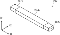
以上の工程を経ると、集合導線207が得られる。
図13に示すように、集合導線207は、一端部207aと他端部207cとを有する。図13及び図14は、実施の形態1にかかる被膜集合導線の製造方法を用いて製造される集合導線の一例を示す模式図である。一端部207aは、側面207eを有し、他端部207cは、側面207fを有する。なお、図13及び図14では、分かり易くするために、集合導線207は1本の導線として図示されている。
図14に示すように、側面207eと側面207fとが交差して成す捻れ角度βは、角度α(図23参照)よりも小さく、被膜集合導線として良好な値の範囲内に収まる。すなわち、集合導線207の捻じれ角度は小さいため、外部被膜形成工程S7において生じ得た集合導線207の捻れ変形は矯正されたと考えられる。
Through the above steps, the
As shown in FIG. 13, the
As shown in FIG. 14, the twist angle β formed by the intersection of the
以上、実施の形態1にかかる被膜集合導線の製造方法によれば、捻れ変形が矯正された被膜集合導線を製造することができる。 As described above, according to the method for manufacturing a film assembly conductor according to the first embodiment, it is possible to manufacture a film assembly conductor in which torsional deformation is corrected.
なお、得られた集合導線207を用いて、モータを形成することができる。
具体的には、集合導線をエアーブローを用いて冷却した後で、プレス成形を用いて、例えば、略「コ」の字状、略「C」の字状、又は、略「U」の字状に曲げられたショートコイル線(図示略)を成形する。ステータ本体のスロットに挿入した後で、拡張する。ショートコイル線の端部同士を溶接し、コイルを形成する。形成したコイルをステータ(図示略)等に配置する等して、モータ(図示略)を形成することができる。例えば、集合導線207の捻り変形が小さいので、集合導線207は、良好な組み付け精度で、ステータ本体等に組み付けられる。したがって、集合導線を良好な精度で組み付けられたモータを製造することができる。このようなモータは、例えば、ハイブリッド自動車等の車両やロボットに搭載されることによって、利用される。
A motor can be formed using the obtained
Specifically, after cooling the collective conducting wire using air blow, for example, using a press molding, for example, a substantially “U” shape, a substantially “C” shape, or a substantially “U” shape. A short coil wire (not shown) bent into a shape is formed. After being inserted into the slot of the stator body, it is expanded. The ends of the short coil wire are welded together to form a coil. A motor (not shown) can be formed by placing the formed coil on a stator (not shown) or the like. For example, since the torsional deformation of the
実施の形態2.
図15〜図17を参照して、実施の形態2にかかる被膜集合導線の製造方法について説明する。図15は、実施の形態2にかかる被膜集合導線の製造方法の一工程を示すフローチャートである。図16は、実施の形態2にかかる被膜集合導線の製造方法の一工程で用いたクランプユニットの正面図である。図17は、実施の形態2にかかる被膜集合導線の製造方法の一工程を示す模式図である。実施の形態2にかかる被膜集合導線の製造方法は、アニール処理工程S13の代わりにアニール処理工程S213を実施することを除いて、実施の形態1にかかる被膜集合導線の製造方法と同じ工程を有する。
With reference to FIGS. 15-17, the manufacturing method of the film assembly conducting
まず、単線圧延工程S1〜剥離工程S12を、実施の形態1にかかる被膜集合導線の製造方法と同様に、実施する。 First, the single wire rolling step S <b> 1 to the peeling step S <b> 12 are performed in the same manner as in the method for manufacturing the coated film conductor according to the first embodiment.
続いて、部分被膜集合導線206に張力を付与しつつ、アニール処理温度に達するまで加熱して、所定時間保持する(アニール処理工程S213)。
Subsequently, while applying tension to the partial coating
具体的には、まず、図16に示すように、クランプユニット30を用いて、部分被膜集合導線206に張力を付与する(クランプ工程S2131)。
クランプユニット30は、DH(Direct resistance Heating:直接通電加熱)電源28及び導線29を含むところを除いて、クランプユニット20と同じ構成を有する。クランプユニット30はDH電源28を含み、DH電源28はクランプ支持部22、26及び導線29を介してクランプ23、27とそれぞれ脱着可能に接続されている。導線29は、部分被膜集合導線206の一端部及び他端部と電気的に接続されている。DH電源28は導線29を介して、電流を部分被膜集合導線206に供給する。クランプ工程S131と同様に、部分被膜集合導線206の両端部をクランプユニット30のクランプ23、27にそれぞれクランプさせることで、部分被膜集合導線206に張力を付与する。
Specifically, first, as shown in FIG. 16, tension is applied to the partial coating
The
続いて、部分被膜集合導線206を直接通電加熱によって加熱する(直接通電加熱工程S2132)。具体的には、DH電源28によって、電流を部分被膜集合導線206に供給し、部分被膜集合導線206の内部、例えば、集合導線206bにジュール熱を生じさせる。これによって、部分被膜集合導線206を、アニール処理温度又はその近傍に達するまで昇温させる。
ところで、上記した炉加熱保持工程S132でのアニール炉40(図12参照)による加熱のように、部分被膜集合導線206の外部から加熱を行う場合、絶縁被膜206aが断熱材として作用するため、集合導線206bと絶縁被膜206aとの接触部に熱が伝わりにくい。
したがって、直接通電加熱工程S2132での直接通電加熱による加熱は、炉加熱保持工程S132でのアニール炉40(図12参照)による加熱と比較して、短時間で多大な熱を被加熱物に発生させる傾向にある。したがって、部分被膜集合導線206を、短時間でアニール処理温度に達するように昇温させることができる。
なお、直接通電加熱工程S2132は、アニール炉40の炉室内又は炉室外で行ってもよい。
Subsequently, the partial film
By the way, when heating is performed from the outside of the partial coating
Therefore, heating by direct current heating in the direct current heating step S2132 generates much heat in the heated object in a short time compared to heating by the annealing furnace 40 (see FIG. 12) in the furnace heating holding step S132. It tends to make it. Therefore, the temperature of the partial film
Note that the direct current heating step S2132 may be performed in the furnace chamber of the
最後に、図17に示すように、部分被膜集合導線206をクランプユニット30ごと、アニール炉40に入れて、加熱保持する(炉加熱保持工程S2133)。
具体的には、DH電源28及び導線29をクランプ支持部22、26から取り外す。その後、炉加熱保持工程S132と同様に、部分被膜集合導線206をクランプしたクランプユニット30を、アニール炉40の内側に配置されたコンベア10に載せる。アニール炉40によって、部分被膜集合導線206がアニール処理温度を維持しつつ、コンベア10が、回転ロール11、12を同じ方向に回転させて、ベルト13を移動させる。これによって、複数のクランプユニット20をアニール炉40を通過させて、複数の部分被膜集合導線206に連続的にアニール処理を施すことができる。
なお、必要に応じて、DH電源28及び導線29をクランプ支持部22、26に着けたまま、部分被膜集合導線206をクランプしたクランプユニット30を、アニール炉40の内側に配置されたコンベア10に載せてもよい。
Finally, as shown in FIG. 17, the partial film
Specifically, the
If necessary, the
ところで、直接通電加熱工程S2132の完了後において、部分被膜集合導線206の一端部及び他端部は、他の部分と比較して、昇温し難い傾向にあり、低い温度であることが多い。この一因として、クランプ支持部22、26と、クランプ23、27との熱容量が、部分被膜集合導線206の熱容量と比較して大きいことが挙げられる。炉加熱保持工程S2133では、アニール炉40が、部分被膜集合導線206及びクランプユニット30を均一に加熱するため、部分被膜集合導線206をその部位によらず、均一に加熱保持することができる。
By the way, after the completion of the direct energization heating step S2132, the one end and the other end of the partial film
以上、実施の形態2にかかる被膜集合導線の製造方法によれば、直接通電加熱によってアニール処理温度まで昇温させることによって、捻れ変形が矯正された被膜集合導線を高い生産性で製造することができる。 As described above, according to the method for manufacturing a film assembly conductor according to the second embodiment, it is possible to manufacture a film assembly conductor whose twist deformation has been corrected with high productivity by raising the temperature to the annealing temperature by direct current heating. it can.
(実施例)
次に、図18を用いて、実施の形態1にかかる被膜集合導線の製造方法を用いて製造した実施例について説明する。図18は、測定位置に対する捻れ角度を示すグラフである。
(Example)
Next, the Example manufactured using the manufacturing method of the film assembly conducting
実施例1では、実施の形態1にかかる被膜集合導線の製造方法を用いて、集合導線を製造した。なお、比較例1では、アニール処理工程S13を除いて実施の形態1にかかる被膜集合導線の製造方法と同じ工程を有する製造方法を用いて、集合導線を製造した。具体的には、比較例1では、アニール処理工程S13に対応する工程において、クランプユニット等を用いて張力を付与することなく、アニール炉を用いてそのまま加熱保持することによって、アニール処理を行なった。 In Example 1, the assembly conductor was manufactured using the method for manufacturing a coated assembly conductor according to the first embodiment. In Comparative Example 1, the assembly conductor was manufactured using a manufacturing method having the same steps as the method for manufacturing the film assembly conductor according to the first embodiment except for the annealing step S13. Specifically, in the comparative example 1, in the process corresponding to the annealing process S13, the annealing process was performed by heating and holding as it was without using a clamp unit or the like to apply a tension. .
実施例1では、剥離工程S12が完了した後、アニール処理工程S13が開始する前に、部分被膜集合導線の捻れ角度を測定した。以後、部分被膜集合導線は、アニール未処理品と記載する。また、実施例1の捻れ角度と比較例1の捻れ角度とを測定した。これらの測定結果を図18に示した。なお、測定位置は、被膜集合導線の一端から他端までの距離である。捻れ角度の良好な範囲は、上限+2deg、下限−2degとした。捻れ角度が良好な範囲にあると、集合導線は、良好な精度でモータなどに組み付けられる。 In Example 1, after the peeling step S12 was completed and before the annealing treatment step S13 was started, the twist angle of the partial coating collective conducting wire was measured. Hereinafter, the partially coated assembly conductor is referred to as an annealed product. Further, the twist angle of Example 1 and the twist angle of Comparative Example 1 were measured. The measurement results are shown in FIG. Note that the measurement position is the distance from one end to the other end of the coated film conductor. The preferable range of the twist angle was an upper limit +2 deg and a lower limit -2 deg. When the twist angle is in a good range, the collective conducting wire is assembled to a motor or the like with good accuracy.
図18に示すように、実施例1では、捻れ角度が、アニール未処理品の捻れ角度と比較して、小さかった。実施例1では、捻れ角度が、アニール処理工程S13によって、減少した。また、実施例1では、捻れ角度が、全域にわたって捻れ角度の良好な範囲内にある。したがって、実施例1の集合導線は、良好な精度でモータなどに組み付けられる。 As shown in FIG. 18, in Example 1, the twist angle was smaller than the twist angle of the untreated annealed product. In Example 1, the twist angle was decreased by the annealing treatment step S13. Moreover, in Example 1, the twist angle is within a favorable range of the twist angle over the entire region. Therefore, the collective conducting wire of Example 1 is assembled to a motor or the like with good accuracy.
一方、比較例1では、捻れ角度が、アニール未処理品の捻れ角度と比較して、大きかった。比較例1では、捻れ角度が、上記したアニール処理工程S13に対応する工程によって、増加したと考えられる。 On the other hand, in Comparative Example 1, the twist angle was larger than the twist angle of the annealed untreated product. In Comparative Example 1, it is considered that the twist angle was increased by the process corresponding to the annealing process S13 described above.
(実験例)
次に、図19を用いて、実験例について説明する。図19は、加熱時間に対する温度を示すグラフである。
(Experimental example)
Next, an experimental example will be described with reference to FIG. FIG. 19 is a graph showing temperature with respect to heating time.
実験例1では、絶縁被膜206aの無い部分被膜集合導線206(図10参照)と同じ構成を有する集合導線を、恒温槽を用いて加熱保持した。なお、恒温槽は、熱風を発生させることによって、恒温槽内に配置された被加熱物を加熱することができる。集合導線を加熱する。この加熱保持した、絶縁被膜を有していない集合導線は、集合導線206bと同じ構成を有し、複数の銅線からなる。また、アニール処理温度は、約320℃であった。
In Experimental Example 1, an assembly conductor having the same configuration as the partially coated assembly conductor 206 (see FIG. 10) without the insulating
また、実験例2では、部分被膜集合導線206(図10参照)と同じ構成を有する集合導線を、実験例1と同様に恒温槽(図示略)を用いて加熱保持した。この加熱保持した集合導線は、複数の銅線からなる集合導線と、フッ素系樹脂からなる絶縁被膜とを含む。また、ここでのアニール処理温度は、約320℃であった。 Further, in Experimental Example 2, the collective conducting wire having the same configuration as the partial coating collective conducting wire 206 (see FIG. 10) was heated and held using a thermostat (not shown) as in Experimental Example 1. The heat-collected collective conducting wire includes a collective conducting wire made of a plurality of copper wires and an insulating coating made of a fluorine-based resin. Moreover, the annealing temperature here was about 320 degreeC.
さらに、実験例3では、実施の形態2にかかる製造方法の直接通電加熱工程S2132(図15参照)と同様に、部分被膜集合導線206(図10参照)と同じ構成を有する集合導線を、直接通電加熱によって加熱した。この加熱保持した集合導線は、複数の銅線からなる集合導線と、フッ素系樹脂からなる絶縁被膜とを含む。また、ここでのアニール処理温度は、約320℃であった。 Furthermore, in Experimental Example 3, as in the direct current heating step S2132 (see FIG. 15) of the manufacturing method according to the second embodiment, an assembly conductor having the same configuration as the partial coating assembly conductor 206 (see FIG. 10) is directly used. Heated by electrical heating. The heat-collected collective conducting wire includes a collective conducting wire made of a plurality of copper wires and an insulating coating made of a fluorine-based resin. Moreover, the annealing temperature here was about 320 degreeC.
実験例1〜3の加熱を開始して、アニール処理温度に達した後に少なくとも温度が安定するまで、集合導線の温度を計測した。その計測結果を図19に示した。 The heating of Experimental Examples 1 to 3 was started, and the temperature of the collective conducting wire was measured until the temperature was stabilized at least after reaching the annealing temperature. The measurement results are shown in FIG.
実験例1及び実験例2では、集合導線の温度がアニール処理温度に到達するまで、約2分間が経過した。一方、実験例3では、集合導線の温度がアニール処理温度に到達するまで、約0.1分間が経過した。したがって、実験例3は、実験例1及び実験例2と比較して、集合導線の温度がアニール処理温度に到達するまでの経過時間が短かった。すなわち、実験例3では、昇温速度が、実験例1の昇温速度及び実験例2の昇温速度と比較して、高かった。この一因として、直接通電加熱は、集合導線にジュール熱を発生させるため、恒温槽やアニール炉による加熱と比較して、高い速度で昇温させやすい傾向にあることが挙げられる。 In Experimental Example 1 and Experimental Example 2, about 2 minutes passed until the temperature of the assembly conductor reached the annealing temperature. On the other hand, in Experimental Example 3, it took about 0.1 minutes until the temperature of the assembly conductor reached the annealing temperature. Therefore, in Experimental Example 3, compared with Experimental Example 1 and Experimental Example 2, the elapsed time until the temperature of the collective conducting wire reached the annealing temperature was shorter. That is, in Experimental Example 3, the temperature increase rate was higher than the temperature increase rate in Experimental Example 1 and the temperature increase rate in Experimental Example 2. One reason for this is that direct current heating tends to increase the temperature at a higher rate than heating by a thermostatic bath or annealing furnace because Joule heat is generated in the collective conducting wire.
なお、本発明は上記実施の形態に限られたものではなく、趣旨を逸脱しない範囲で適宜変更することが可能である。例えば、実施の形態1及び2にかかる集合導線の製造方法では、切断工程S10〜アニール処理工程S13を実施したが、切断工程S10〜アニール処理工程S13の代わりにアニール処理工程S313を実施してもよい。アニール処理工程S313は、図20に示すアニール処理装置50を用いて、実施することができる。アニール処理装置50は、炉室51と、保持台52と、保持台52の両端部にそれぞれ設けられる2つのロール支持部53と、ロール支持部53に回転可能にそれぞれ支持される2つのロール54とを有する。2つのロール54は、それぞれ、回転、逆回転、停止することが可能な技術的な手段が設けられている。2つのロール54は、それぞれ、部分被膜集合導線206の端部をそれぞれ巻き付けられている。ロール54同士が互いに逆向きに回転することで、部分被膜集合導線206に張力を付与することができる。
ここで、部分被膜集合導線206を、真っ直ぐに延ばすように張力をかける。部分被膜集合導線206の他端部は、部分被膜集合導線206の一端部に対して、捻れないようにするとよい。言い換えると、捻れ角度、つまり、部分被膜集合導線206の他端部の部分被膜集合導線206の一端部に対する角度が実質的に0(ゼロ)°であると好ましい。
炉室51を加熱保持することで、アニール処理を行うことができる。また、このような集合導線の製造方法によれば、切断工程S10〜剥離工程S12を省略しても、アニール処理を行うことができる。
なお、少なくとも一方のロール支持部53を移動させる機構を設けて、ロール54の回転を停止した状態でロール支持部53同士の距離を変化させることによって、部分被膜集合導線206に張力を付与してもよい。
Note that the present invention is not limited to the above-described embodiment, and can be changed as appropriate without departing from the spirit of the present invention. For example, in the manufacturing method of the collective conducting wire according to the first and second embodiments, the cutting process S10 to the annealing process S13 is performed, but the annealing process S313 may be performed instead of the cutting process S10 to the annealing process S13. Good. The annealing process S313 can be performed using the
Here, a tension is applied so that the partial film
Annealing treatment can be performed by heating and holding the
In addition, by providing a mechanism for moving at least one
また、実施の形態1及び2にかかる集合導線の製造方法では、単線圧延工程S1〜アニール処理工程S13、S132を実施したが、必要に応じて、単線圧延工程S1〜剥離工程S12の少なくとも一工程の実施を省略してもよい。また、実施の形態1及び2にかかる集合導線の製造方法では、張力を付与した状態でアニール処理を行ったが、アニール処理開始と同時、またはアニール処理開始後に張力を付与してもよい。
Moreover, in the manufacturing method of the assembly conducting
20、30 クランプユニット 23、27 クランプ
40 アニール炉 50 アニール処理装置
199 素線群 200 集合導線束
201 集合導体
201a 平行部 201b 左巻部
201c 右巻部
205 短尺集合導線
206 部分被膜集合導線
206a 絶縁被膜 206b 集合導線
207 集合導線
207a 一端部 207c 他端部
207e 側面 207f 側面
S3 束形成工程 S4 捻り工程
S7 外部被膜形成工程
S13、S213、S313 アニール処理工程
S131、S2131 クランプ工程
S2132 直接通電加熱工程
S132、S2133 炉加熱保持工程
20, 30
205 Short-
S13, S213, S313 Annealing treatment step S131, S2131 Clamping step S2132 Direct current heating step S132, S2133 Furnace heating and holding step
Claims (4)
前記集合導線を絶縁被膜で被覆することによって被膜集合導線を形成する工程と、
前記被膜集合導線に張力を付与しつつ、前記被膜集合導線をアニール処理温度で加熱保持するアニール処理工程と、
を含む被膜集合導線の製造方法。 Forming a conducting wire having a right-handed portion, a parallel portion, and a left-handed portion by twisting and deforming a conducting wire bundle formed by bundling a plurality of conducting wires;
Forming a film assembly conductor by coating the assembly conductor with an insulating coating;
An annealing treatment step of heating and holding the coating assembly wire at an annealing temperature while applying tension to the coating assembly wire;
The manufacturing method of the film | membrane assembly conducting wire containing this.
前記アニール処理工程は、前記被膜集合導線をアニール処理温度まで昇温させる加熱工程を含み、
前記加熱工程では、前記被膜集合導線の前記通電部に電流を供給することによって、直接通電加熱を行う
ことを特徴とする請求項1に記載の被膜集合導線の製造方法。 The film assembly conducting wire has a current-carrying portion that exposes the assembly conducting wire at both ends,
The annealing treatment step includes a heating step of raising the film assembly conducting wire to an annealing treatment temperature,
The method for manufacturing a film assembly conductor according to claim 1, wherein in the heating step, direct current heating is performed by supplying a current to the energization portion of the film assembly conductor.
ことを特徴とする請求項1又は2に記載の被膜集合導線の製造方法。 In the annealing treatment step, the film assembly conducting wire is fixed in a state where both ends of the film assembly conducting wire are fixed so that the twist angle due to the twist back deformation generated in the film assembly conducting wire forming step is substantially zero. A method for producing a film assembly conductor according to claim 1, wherein tension is applied to the wire assembly.
前記被膜集合導線を切断することによって、短尺化させる工程をさらに含む
ことを特徴とする請求項1〜3のいずれか1項に記載の被膜集合導線の製造方法。 Before the annealing process,
The method for producing a film assembly conductor according to any one of claims 1 to 3, further comprising a step of shortening the film assembly conductor by cutting the film assembly conductor.
Priority Applications (4)
| Application Number | Priority Date | Filing Date | Title |
|---|---|---|---|
| JP2015100919A JP6179552B2 (en) | 2015-05-18 | 2015-05-18 | Method for manufacturing coated film conductor |
| CN201610320483.2A CN106169846B (en) | 2015-05-18 | 2016-05-16 | The manufacturing method of overlay film set conducting wire |
| US15/155,484 US10163551B2 (en) | 2015-05-18 | 2016-05-16 | Methods of manufacturing a coated conducting wire assembly |
| EP16169960.8A EP3096440B1 (en) | 2015-05-18 | 2016-05-17 | Manufacturing method of coated conducting wire assembly |
Applications Claiming Priority (1)
| Application Number | Priority Date | Filing Date | Title |
|---|---|---|---|
| JP2015100919A JP6179552B2 (en) | 2015-05-18 | 2015-05-18 | Method for manufacturing coated film conductor |
Publications (2)
| Publication Number | Publication Date |
|---|---|
| JP2016219176A JP2016219176A (en) | 2016-12-22 |
| JP6179552B2 true JP6179552B2 (en) | 2017-08-16 |
Family
ID=56014867
Family Applications (1)
| Application Number | Title | Priority Date | Filing Date |
|---|---|---|---|
| JP2015100919A Expired - Fee Related JP6179552B2 (en) | 2015-05-18 | 2015-05-18 | Method for manufacturing coated film conductor |
Country Status (4)
| Country | Link |
|---|---|
| US (1) | US10163551B2 (en) |
| EP (1) | EP3096440B1 (en) |
| JP (1) | JP6179552B2 (en) |
| CN (1) | CN106169846B (en) |
Families Citing this family (10)
| Publication number | Priority date | Publication date | Assignee | Title |
|---|---|---|---|---|
| CN109923621B (en) * | 2016-11-08 | 2021-02-09 | 株式会社自动网络技术研究所 | Electric wire conductor, coated electric wire, and wire harness |
| US10354777B2 (en) * | 2017-09-21 | 2019-07-16 | Schlumberger Technology Corporation | Electrical conductors and processes for making and using same |
| DE102017125887A1 (en) * | 2017-11-06 | 2019-05-09 | Thyssenkrupp Ag | Method and device for producing strands, strand and electrical machine |
| KR20190083725A (en) * | 2018-01-05 | 2019-07-15 | 현대자동차주식회사 | Vehicular hairpin winding motor for enhancing energy efficiency and manufacturing method |
| DE102018208407A1 (en) * | 2018-05-28 | 2019-11-28 | Thyssenkrupp Ag | Method for producing stranded wire, method for producing an electric motor, and use of stranded wire |
| DE102018211867A1 (en) | 2018-07-17 | 2020-01-23 | Thyssenkrupp Ag | Process for the heat treatment of a stranded wire, and process for producing an electric motor or motor vehicle |
| DE102020133307A1 (en) | 2020-12-14 | 2022-06-15 | Dr. Ing. H.C. F. Porsche Aktiengesellschaft | Stator assembly and method for its manufacture |
| US12573903B2 (en) | 2022-09-19 | 2026-03-10 | Caterpillar Inc. | Switched reluctance motor manufacture with variable wire twist rate |
| WO2025113729A1 (en) * | 2023-11-29 | 2025-06-05 | Schaeffler Technologies AG & Co. KG | Stator winding wire and high-voltage-terminal stator winding wire |
| CN119694675B (en) * | 2025-01-08 | 2025-10-17 | 合隆新材料科技(江苏)有限公司 | Heating device for copper-clad steel ground strand production |
Family Cites Families (10)
| Publication number | Priority date | Publication date | Assignee | Title |
|---|---|---|---|---|
| JPS60137536A (en) * | 1983-12-26 | 1985-07-22 | Sumitomo Electric Ind Ltd | Method and device for twisting irregularly shaped wires |
| JPH0689622A (en) * | 1992-09-09 | 1994-03-29 | Furukawa Electric Co Ltd:The | Manufacturing method of stranded wire for wiring |
| JPH08223840A (en) * | 1995-02-17 | 1996-08-30 | Toyota Motor Corp | Coil winding material and manufacturing method thereof |
| DE10100649A1 (en) * | 2001-01-09 | 2002-07-11 | Nexans France S A | Method of making a multi-wire conductor |
| JP5306994B2 (en) * | 2007-03-30 | 2013-10-02 | 古河電気工業株式会社 | Insulated wire manufacturing method and apparatus |
| JP5309595B2 (en) * | 2008-02-19 | 2013-10-09 | 住友電気工業株式会社 | Motor, reactor using conductive wire as coil, and method for manufacturing said conductive wire |
| JP5954243B2 (en) * | 2013-04-19 | 2016-07-20 | トヨタ自動車株式会社 | Method for manufacturing aggregate conductor |
| JP2015050083A (en) * | 2013-09-03 | 2015-03-16 | トヨタ自動車株式会社 | Twisted structure of collective conductor |
| JP2015080281A (en) * | 2013-10-15 | 2015-04-23 | トヨタ自動車株式会社 | Assembled conductor and motor |
| JP2016024974A (en) * | 2014-07-22 | 2016-02-08 | トヨタ自動車株式会社 | Collective conducting wire and manufacturing method thereof |
-
2015
- 2015-05-18 JP JP2015100919A patent/JP6179552B2/en not_active Expired - Fee Related
-
2016
- 2016-05-16 CN CN201610320483.2A patent/CN106169846B/en not_active Expired - Fee Related
- 2016-05-16 US US15/155,484 patent/US10163551B2/en active Active
- 2016-05-17 EP EP16169960.8A patent/EP3096440B1/en active Active
Also Published As
| Publication number | Publication date |
|---|---|
| CN106169846A (en) | 2016-11-30 |
| US10163551B2 (en) | 2018-12-25 |
| EP3096440B1 (en) | 2019-12-11 |
| CN106169846B (en) | 2019-01-04 |
| JP2016219176A (en) | 2016-12-22 |
| EP3096440A1 (en) | 2016-11-23 |
| US20160343475A1 (en) | 2016-11-24 |
Similar Documents
| Publication | Publication Date | Title |
|---|---|---|
| JP6179552B2 (en) | Method for manufacturing coated film conductor | |
| US20080314473A1 (en) | Electric wire delivery apparatus and electric wire sizing-cutting apparatus including the same | |
| US10128728B2 (en) | Manufacturing method for segment coil | |
| US11349378B2 (en) | Coil segment cutting method and coil segment cutting apparatus | |
| US8350441B2 (en) | Motor including wires with insulating tubes and method of manufacturing motor | |
| CN107438887B (en) | Superconducting wire and method for manufacturing superconducting wire | |
| JP6112714B2 (en) | Coil manufacturing equipment | |
| CN109382465B (en) | Wire straightening device | |
| CN101983471A (en) | Motor winding manufacturing equipment | |
| JP2017508237A5 (en) | ||
| JP4836056B2 (en) | Coil component manufacturing method and coil component manufacturing apparatus | |
| EP3021467A1 (en) | Method and station for the construction of a stator winding with rigid bars for a rotary electrical machine | |
| JP6035378B1 (en) | Litz wire coil | |
| JP2016024974A (en) | Collective conducting wire and manufacturing method thereof | |
| CN104575862B (en) | The method for making insulated electric conductor shape and anneal | |
| CN106233591A (en) | For manufacturing the method and apparatus of the winding of the winding support of motor, winding support and motor | |
| CN114616734B (en) | Device and method for stripping square wire coating resin layer | |
| TW202033051A (en) | Method for manufacturing carbon nanotube device, carbon nanotube device and carbon nanotube heater | |
| WO2015056077A2 (en) | Manufacturing method for collective conducting wire and motor | |
| CN105206353B (en) | The manufacture method and flat cable of flat cable | |
| JPWO2019207989A1 (en) | Insulation film peeling device and insulation film peeling method | |
| JP2008210532A (en) | Coil for electromagnetic induction heating, fixing device, and manufacturing method of coil for electromagnetic induction heating | |
| CN103545035B (en) | Electric wire | |
| JP6558538B2 (en) | Wire connection method | |
| JP2024077169A (en) | Leveller and coil payout device, method for straightening coiled metal material, method for manufacturing stamped metal material, and method for manufacturing insulated circuit board |
Legal Events
| Date | Code | Title | Description |
|---|---|---|---|
| A621 | Written request for application examination |
Free format text: JAPANESE INTERMEDIATE CODE: A621 Effective date: 20160923 |
|
| A977 | Report on retrieval |
Free format text: JAPANESE INTERMEDIATE CODE: A971007 Effective date: 20170607 |
|
| TRDD | Decision of grant or rejection written | ||
| A01 | Written decision to grant a patent or to grant a registration (utility model) |
Free format text: JAPANESE INTERMEDIATE CODE: A01 Effective date: 20170620 |
|
| A61 | First payment of annual fees (during grant procedure) |
Free format text: JAPANESE INTERMEDIATE CODE: A61 Effective date: 20170703 |
|
| R151 | Written notification of patent or utility model registration |
Ref document number: 6179552 Country of ref document: JP Free format text: JAPANESE INTERMEDIATE CODE: R151 |
|
| LAPS | Cancellation because of no payment of annual fees |