JP6177155B2 - Oscillator circuit and frequency synthesizer - Google Patents
Oscillator circuit and frequency synthesizer Download PDFInfo
- Publication number
- JP6177155B2 JP6177155B2 JP2014023064A JP2014023064A JP6177155B2 JP 6177155 B2 JP6177155 B2 JP 6177155B2 JP 2014023064 A JP2014023064 A JP 2014023064A JP 2014023064 A JP2014023064 A JP 2014023064A JP 6177155 B2 JP6177155 B2 JP 6177155B2
- Authority
- JP
- Japan
- Prior art keywords
- value
- code value
- frequency
- frequency control
- circuit
- Prior art date
- Legal status (The legal status is an assumption and is not a legal conclusion. Google has not performed a legal analysis and makes no representation as to the accuracy of the status listed.)
- Active
Links
- 230000010355 oscillation Effects 0.000 claims description 138
- 230000035945 sensitivity Effects 0.000 claims description 41
- 239000003990 capacitor Substances 0.000 claims description 40
- 230000001186 cumulative effect Effects 0.000 claims description 37
- 230000008859 change Effects 0.000 claims description 30
- 238000001514 detection method Methods 0.000 claims description 20
- 230000003247 decreasing effect Effects 0.000 claims description 2
- 101001020552 Rattus norvegicus LIM/homeobox protein Lhx1 Proteins 0.000 description 18
- 238000010586 diagram Methods 0.000 description 18
- 238000004364 calculation method Methods 0.000 description 12
- 230000000694 effects Effects 0.000 description 6
- 238000006243 chemical reaction Methods 0.000 description 5
- 230000007423 decrease Effects 0.000 description 5
- 230000004048 modification Effects 0.000 description 4
- 238000012986 modification Methods 0.000 description 4
- 239000004065 semiconductor Substances 0.000 description 3
- 230000007704 transition Effects 0.000 description 3
- 230000009471 action Effects 0.000 description 2
- 238000005516 engineering process Methods 0.000 description 2
- 229920006395 saturated elastomer Polymers 0.000 description 2
- 230000015556 catabolic process Effects 0.000 description 1
- 230000000052 comparative effect Effects 0.000 description 1
- 238000004519 manufacturing process Methods 0.000 description 1
- 238000000034 method Methods 0.000 description 1
- 230000009467 reduction Effects 0.000 description 1
Images


Classifications
-
- H—ELECTRICITY
- H03—ELECTRONIC CIRCUITRY
- H03L—AUTOMATIC CONTROL, STARTING, SYNCHRONISATION OR STABILISATION OF GENERATORS OF ELECTRONIC OSCILLATIONS OR PULSES
- H03L7/00—Automatic control of frequency or phase; Synchronisation
- H03L7/06—Automatic control of frequency or phase; Synchronisation using a reference signal applied to a frequency- or phase-locked loop
- H03L7/08—Details of the phase-locked loop
- H03L7/083—Details of the phase-locked loop the reference signal being additionally directly applied to the generator
-
- H—ELECTRICITY
- H03—ELECTRONIC CIRCUITRY
- H03B—GENERATION OF OSCILLATIONS, DIRECTLY OR BY FREQUENCY-CHANGING, BY CIRCUITS EMPLOYING ACTIVE ELEMENTS WHICH OPERATE IN A NON-SWITCHING MANNER; GENERATION OF NOISE BY SUCH CIRCUITS
- H03B5/00—Generation of oscillations using amplifier with regenerative feedback from output to input
- H03B5/08—Generation of oscillations using amplifier with regenerative feedback from output to input with frequency-determining element comprising lumped inductance and capacitance
- H03B5/12—Generation of oscillations using amplifier with regenerative feedback from output to input with frequency-determining element comprising lumped inductance and capacitance active element in amplifier being semiconductor device
- H03B5/1206—Generation of oscillations using amplifier with regenerative feedback from output to input with frequency-determining element comprising lumped inductance and capacitance active element in amplifier being semiconductor device using multiple transistors for amplification
-
- H—ELECTRICITY
- H03—ELECTRONIC CIRCUITRY
- H03B—GENERATION OF OSCILLATIONS, DIRECTLY OR BY FREQUENCY-CHANGING, BY CIRCUITS EMPLOYING ACTIVE ELEMENTS WHICH OPERATE IN A NON-SWITCHING MANNER; GENERATION OF NOISE BY SUCH CIRCUITS
- H03B5/00—Generation of oscillations using amplifier with regenerative feedback from output to input
- H03B5/08—Generation of oscillations using amplifier with regenerative feedback from output to input with frequency-determining element comprising lumped inductance and capacitance
- H03B5/12—Generation of oscillations using amplifier with regenerative feedback from output to input with frequency-determining element comprising lumped inductance and capacitance active element in amplifier being semiconductor device
- H03B5/1237—Generation of oscillations using amplifier with regenerative feedback from output to input with frequency-determining element comprising lumped inductance and capacitance active element in amplifier being semiconductor device comprising means for varying the frequency of the generator
- H03B5/124—Generation of oscillations using amplifier with regenerative feedback from output to input with frequency-determining element comprising lumped inductance and capacitance active element in amplifier being semiconductor device comprising means for varying the frequency of the generator the means comprising a voltage dependent capacitance
-
- H—ELECTRICITY
- H03—ELECTRONIC CIRCUITRY
- H03B—GENERATION OF OSCILLATIONS, DIRECTLY OR BY FREQUENCY-CHANGING, BY CIRCUITS EMPLOYING ACTIVE ELEMENTS WHICH OPERATE IN A NON-SWITCHING MANNER; GENERATION OF NOISE BY SUCH CIRCUITS
- H03B5/00—Generation of oscillations using amplifier with regenerative feedback from output to input
- H03B5/08—Generation of oscillations using amplifier with regenerative feedback from output to input with frequency-determining element comprising lumped inductance and capacitance
- H03B5/12—Generation of oscillations using amplifier with regenerative feedback from output to input with frequency-determining element comprising lumped inductance and capacitance active element in amplifier being semiconductor device
- H03B5/1237—Generation of oscillations using amplifier with regenerative feedback from output to input with frequency-determining element comprising lumped inductance and capacitance active element in amplifier being semiconductor device comprising means for varying the frequency of the generator
- H03B5/1262—Generation of oscillations using amplifier with regenerative feedback from output to input with frequency-determining element comprising lumped inductance and capacitance active element in amplifier being semiconductor device comprising means for varying the frequency of the generator the means comprising switched elements
- H03B5/1265—Generation of oscillations using amplifier with regenerative feedback from output to input with frequency-determining element comprising lumped inductance and capacitance active element in amplifier being semiconductor device comprising means for varying the frequency of the generator the means comprising switched elements switched capacitors
-
- H—ELECTRICITY
- H03—ELECTRONIC CIRCUITRY
- H03L—AUTOMATIC CONTROL, STARTING, SYNCHRONISATION OR STABILISATION OF GENERATORS OF ELECTRONIC OSCILLATIONS OR PULSES
- H03L7/00—Automatic control of frequency or phase; Synchronisation
- H03L7/06—Automatic control of frequency or phase; Synchronisation using a reference signal applied to a frequency- or phase-locked loop
- H03L7/08—Details of the phase-locked loop
- H03L7/085—Details of the phase-locked loop concerning mainly the frequency- or phase-detection arrangement including the filtering or amplification of its output signal
- H03L7/093—Details of the phase-locked loop concerning mainly the frequency- or phase-detection arrangement including the filtering or amplification of its output signal using special filtering or amplification characteristics in the loop
-
- H—ELECTRICITY
- H03—ELECTRONIC CIRCUITRY
- H03B—GENERATION OF OSCILLATIONS, DIRECTLY OR BY FREQUENCY-CHANGING, BY CIRCUITS EMPLOYING ACTIVE ELEMENTS WHICH OPERATE IN A NON-SWITCHING MANNER; GENERATION OF NOISE BY SUCH CIRCUITS
- H03B2201/00—Aspects of oscillators relating to varying the frequency of the oscillations
- H03B2201/02—Varying the frequency of the oscillations by electronic means
- H03B2201/0275—Varying the frequency of the oscillations by electronic means the means delivering several selected voltages or currents
- H03B2201/0283—Varying the frequency of the oscillations by electronic means the means delivering several selected voltages or currents the means functioning digitally
- H03B2201/0291—Varying the frequency of the oscillations by electronic means the means delivering several selected voltages or currents the means functioning digitally and being controlled by a processing device, e.g. a microprocessor
-
- H—ELECTRICITY
- H03—ELECTRONIC CIRCUITRY
- H03J—TUNING RESONANT CIRCUITS; SELECTING RESONANT CIRCUITS
- H03J2200/00—Indexing scheme relating to tuning resonant circuits and selecting resonant circuits
- H03J2200/10—Tuning of a resonator by means of digitally controlled capacitor bank
Landscapes
- Engineering & Computer Science (AREA)
- Power Engineering (AREA)
- Stabilization Of Oscillater, Synchronisation, Frequency Synthesizers (AREA)
Description
本開示は、デジタル信号により発振周波数を制御する発振回路、およびそのような発振回路を備えた周波数シンセサイザに関する。 The present disclosure relates to an oscillation circuit that controls an oscillation frequency by a digital signal, and a frequency synthesizer including such an oscillation circuit.
半導体装置には、所望の周波数の信号を生成するために、しばしば周波数シンセサイザが搭載される。周波数シンセサイザは、例えばアナログPLL(Phase Locked Loop)により実現することができる。アナログPLLは、アナログの制御電圧に応じて発振周波数を変化させることができる電圧制御発振回路(VCO;Voltage Controlled Oscillator)を含んで構成される。このようなアナログPLLでは、発振周波数が一定になるように、制御電圧が制御されるようになっている。 A semiconductor device is often equipped with a frequency synthesizer in order to generate a signal having a desired frequency. The frequency synthesizer can be realized by an analog PLL (Phase Locked Loop), for example. The analog PLL is configured to include a voltage controlled oscillator (VCO) that can change an oscillation frequency in accordance with an analog control voltage. In such an analog PLL, the control voltage is controlled so that the oscillation frequency is constant.
近年、半導体製造プロセスの世代が進むにつれて、デバイスの耐圧が低下し、それに応じて半導体装置の電源電圧が低下してきている。これにより、アナログPLLでは、電圧制御発振回路の制御電圧の電圧範囲が狭くなってしまうため、広い周波数範囲の発振信号を生成しにくくなってきている。そこで、デジタル信号により発振周波数を制御するデジタル制御発振回路(DCO;Digitally Controlled Oscillator)を有するデジタルPLLがしばしば用いられるようになってきている。例えば、特許文献1には、分数部ビットと整数部ビットとを含む周波数制御ワードに基づいて、上位の可変容量バンクと下位の可変容量バンクの周波数を制御するデジタル制御発振回路が開示されている。
In recent years, as the generation of semiconductor manufacturing processes progresses, the breakdown voltage of the device decreases, and the power supply voltage of the semiconductor device decreases accordingly. As a result, in the analog PLL, the voltage range of the control voltage of the voltage controlled oscillation circuit becomes narrow, and it is difficult to generate an oscillation signal in a wide frequency range. Therefore, a digital PLL having a digitally controlled oscillator (DCO) that controls an oscillation frequency by a digital signal is often used. For example,
ところで、発振回路では、一般に、位相雑音を低減することが望まれており、デジタル制御発振回路においても、位相雑音の低減が期待されている。 By the way, in an oscillation circuit, it is generally desired to reduce phase noise, and in a digitally controlled oscillation circuit, reduction of phase noise is expected.
本開示はかかる問題点に鑑みてなされたもので、その目的は、位相雑音を低減することができる発振回路および周波数シンセサイザを提供することにある。 The present disclosure has been made in view of such problems, and an object thereof is to provide an oscillation circuit and a frequency synthesizer that can reduce phase noise.
本開示の発振回路は、演算部と、発振部とを備えている。演算部は、第1の入力コード値を補正することにより、第1の入力コード値のとりうる範囲より狭い第1の所定の範囲内の第1のコード値を生成し、第1の入力コード値の補正量に応じて第2の入力コード値を補正して第2のコード値を生成するものである。発振部は、第1のコード値に基づいて第1の感度で発振信号の周波数が変化し、第2のコード値に基づいて第1の感度よりも高い第2の感度で発振信号の周波数が変化するものである。上記演算部は、比較部と、累積加算部と、補正部とを有している。比較部は、第1のコード値と、第1の所定の範囲よりも狭い第2の所定の範囲の上限値および下限値とを比較して比較結果値を生成するものである。累積加算部は、比較結果値を累積加算して累積値を求めるものである。補正部は、累積値に基づいて第1の入力コード値を補正するとともに第2の入力コード値を補正するものである。
The oscillation circuit of the present disclosure includes a calculation unit and an oscillation unit. The calculation unit corrects the first input code value to generate a first code value within a first predetermined range that is narrower than a range that the first input code value can take, and the first input code value The second code value is generated by correcting the second input code value according to the value correction amount. The oscillation unit changes the frequency of the oscillation signal with the first sensitivity based on the first code value, and the frequency of the oscillation signal with the second sensitivity higher than the first sensitivity based on the second code value. It will change. The calculation unit includes a comparison unit, a cumulative addition unit, and a correction unit. The comparison unit compares the first code value with an upper limit value and a lower limit value of a second predetermined range that is narrower than the first predetermined range, and generates a comparison result value. The cumulative addition unit is configured to cumulatively add the comparison result values to obtain a cumulative value. The correction unit corrects the first input code value based on the accumulated value and corrects the second input code value.
本開示の第1の周波数シンセサイザは、基準位相生成回路と、位相比較回路と、周波数制御回路と、発振回路と、位相検出回路とを備えている。基準位相生成回路は、基準位相信号を生成するものである。位相比較回路は、基準位相信号と帰還位相信号との位相差を検出するものである。周波数制御回路は、位相比較回路における検出結果に基づいて第1の入力コード値および第2の入力コード値を生成するものである。発振回路は、第1の入力コード値および第2の入力コード値に基づいて発振信号を生成するものである。位相検出回路は、発振信号の位相を求めて帰還位相信号として出力するものである。上記発振回路は、演算部と、発振部とを有している。演算部は、第1の入力コード値を補正することにより、第1の入力コード値のとりうる範囲より狭い第1の所定の範囲内の第1のコード値を生成し、第1の入力コード値の補正量に応じて第2の入力コード値を補正して第2のコード値を生成するものである。発振部は、第1のコード値に基づいて第1の感度で発振信号の周波数が変化し、第2のコード値に基づいて第1の感度よりも高い第2の感度で発振信号の周波数が変化するものである。上記演算部は、比較部と、累積加算部と、補正部とを有している。比較部は、第1のコード値と、第1の所定の範囲よりも狭い第2の所定の範囲の上限値および下限値とを比較して比較結果値を生成するものである。累積加算部は、比較結果値を累積加算して累積値を求めるものである。補正部は、累積値に基づいて第1の入力コード値を補正するとともに第2の入力コード値を補正するものである。
The first frequency synthesizer of the present disclosure includes a reference phase generation circuit, a phase comparison circuit, a frequency control circuit, an oscillation circuit, and a phase detection circuit. The reference phase generation circuit generates a reference phase signal. The phase comparison circuit detects a phase difference between the reference phase signal and the feedback phase signal. The frequency control circuit generates a first input code value and a second input code value based on the detection result in the phase comparison circuit. The oscillation circuit generates an oscillation signal based on the first input code value and the second input code value. The phase detection circuit obtains the phase of the oscillation signal and outputs it as a feedback phase signal. The oscillation circuit includes a calculation unit and an oscillation unit. The calculation unit corrects the first input code value to generate a first code value within a first predetermined range that is narrower than a range that the first input code value can take, and the first input code value The second code value is generated by correcting the second input code value according to the value correction amount. The oscillation unit changes the frequency of the oscillation signal with the first sensitivity based on the first code value, and the frequency of the oscillation signal with the second sensitivity higher than the first sensitivity based on the second code value. It will change. The calculation unit includes a comparison unit, a cumulative addition unit, and a correction unit. The comparison unit compares the first code value with an upper limit value and a lower limit value of a second predetermined range that is narrower than the first predetermined range, and generates a comparison result value. The cumulative addition unit is configured to cumulatively add the comparison result values to obtain a cumulative value. The correction unit corrects the first input code value based on the accumulated value and corrects the second input code value.
本開示の第2の周波数シンセサイザは、位相比較回路と、周波数制御回路と、発振回路と、分周回路とを備えている。位相比較回路は、入力クロック信号と帰還クロック信号との間の位相差を検出するものである。周波数制御回路は、位相比較回路における検出結果に基づいて第1の入力コード値および第2の入力コード値を生成するものである。発振回路は、第1の入力コード値および第2の入力コード値に基づいて発振信号を生成するものである。分周回路は、発振信号を分周して帰還クロック信号を生成するものである。上記発振回路は、演算部と、発振部とを有している。演算部は、第1の入力コード値を補正することにより、第1の入力コード値のとりうる範囲より狭い第1の所定の範囲内の第1のコード値を生成し、第1の入力コード値の補正量に応じて第2の入力コード値を補正して第2のコード値を生成するものである。発振部は、第1のコード値に基づいて第1の感度で発振信号の周波数が変化し、第2のコード値に基づいて第1の感度よりも高い第2の感度で発振信号の周波数が変化するものである。上記演算部は、比較部と、累積加算部と、補正部とを有している。比較部は、第1のコード値と、第1の所定の範囲よりも狭い第2の所定の範囲の上限値および下限値とを比較して比較結果値を生成するものである。累積加算部は、比較結果値を累積加算して累積値を求めるものである。補正部は、累積値に基づいて第1の入力コード値を補正するとともに第2の入力コード値を補正するものである。
The second frequency synthesizer of the present disclosure includes a phase comparison circuit, a frequency control circuit, an oscillation circuit, and a frequency divider circuit. The phase comparison circuit detects a phase difference between the input clock signal and the feedback clock signal. The frequency control circuit generates a first input code value and a second input code value based on the detection result in the phase comparison circuit. The oscillation circuit generates an oscillation signal based on the first input code value and the second input code value. The frequency divider circuit divides the oscillation signal to generate a feedback clock signal. The oscillation circuit includes a calculation unit and an oscillation unit. The calculation unit corrects the first input code value to generate a first code value within a first predetermined range that is narrower than a range that the first input code value can take, and the first input code value The second code value is generated by correcting the second input code value according to the value correction amount. The oscillation unit changes the frequency of the oscillation signal with the first sensitivity based on the first code value, and the frequency of the oscillation signal with the second sensitivity higher than the first sensitivity based on the second code value. It will change. The calculation unit includes a comparison unit, a cumulative addition unit, and a correction unit. The comparison unit compares the first code value with an upper limit value and a lower limit value of a second predetermined range that is narrower than the first predetermined range, and generates a comparison result value. The cumulative addition unit is configured to cumulatively add the comparison result values to obtain a cumulative value. The correction unit corrects the first input code value based on the accumulated value and corrects the second input code value.
本開示の発振回路、第1の周波数シンセサイザ、および第2の周波数シンセサイザでは、第1の入力コード値および第2の入力コード値に基づいて第1のコード値および第2のコード値が生成され、これらの第1のコード値および第2のコード値に基づいて発振信号が生成される。その際、第1の入力コード値が補正されることにより、第1の入力コード値のとりうる範囲より狭い第1の所定の範囲内の第1のコード値が生成され、第1の入力コード値の補正量に応じて第2の入力コード値が補正され、第2のコード値が生成される。 In the oscillation circuit, the first frequency synthesizer, and the second frequency synthesizer of the present disclosure, the first code value and the second code value are generated based on the first input code value and the second input code value. The oscillation signal is generated based on the first code value and the second code value. At this time, by correcting the first input code value, a first code value within a first predetermined range that is narrower than the range that the first input code value can take is generated, and the first input code value is generated. The second input code value is corrected according to the value correction amount, and the second code value is generated.
本開示の発振回路および周波数シンセサイザによれば、第1の入力コード値を補正することにより、第1の入力コード値のとりうる範囲より狭い第1の所定の範囲内の第1のコード値を生成し、第1の入力コード値の補正量に応じて第2の入力コード値を補正して第2のコード値を生成したので、位相雑音を低減することができる。なお、ここに記載された効果は必ずしも限定されるものではなく、本開示中に記載されたいずれの効果があってもよい。 According to the oscillation circuit and the frequency synthesizer of the present disclosure, by correcting the first input code value, the first code value within the first predetermined range narrower than the range that the first input code value can take is obtained. Since the second code value is generated by correcting the second input code value according to the correction amount of the first input code value, the phase noise can be reduced. In addition, the effect described here is not necessarily limited, and there may be any effect described in the present disclosure.
以下、本開示の実施の形態について、図面を参照して詳細に説明する。 Hereinafter, embodiments of the present disclosure will be described in detail with reference to the drawings.
[構成例]
(全体構成例)
図1は、第1の実施の形態に係る周波数シンセサイザの一構成例を表すものである。図1では、太線で示した配線は、複数のビットからなるワードを伝えるいわゆるバス配線を示し、細線で示した配線は、1つの信号または差動信号を伝える配線を示す。周波数シンセサイザ1は、デジタル制御発振回路(DCO)を有するデジタルPLLである。なお、本開示の実施の形態に係る発振回路は、本実施の形態により具現化されるので、併せて説明する。
[Configuration example]
(Overall configuration example)
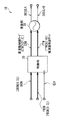
FIG. 1 shows a configuration example of a frequency synthesizer according to the first embodiment. In FIG. 1, a wiring indicated by a thick line indicates a so-called bus wiring that transmits a word composed of a plurality of bits, and a wiring indicated by a thin line indicates a wiring that transmits one signal or differential signal. The
周波数シンセサイザ1は、基準位相生成回路11と、位相比較回路12と、ループフィルタ13と、利得調整回路14と、発振回路15と、位相検出回路16と、リタイミング回路17とを備えている。
The
基準位相生成回路11は、分周比ワードFCWおよびクロック信号CLKに基づいて、基準位相ワードPW1を生成するものである。具体的には、基準位相生成回路11は、分周比ワードFCWが示す値を累積加算して、基準位相値を生成し、その基準位相値を基準位相ワードPW1として出力するようになっている。
The reference
位相比較回路12は、基準位相ワードPW1および位相ワードPW2に基づいて、位相誤差ワードPEWを生成するものである。具体的には、位相比較回路12は、基準位相ワードPW1が示す基準位相値から、位相ワードPW2が示す位相値を減算することにより、位相誤差値を求め、その位相誤差値を位相誤差ワードPEWとして出力するようになっている。
The
ループフィルタ13は、位相誤差ワードPEWおよびクロック信号CLKに基づいて、位相誤差ワードPEW2を生成するものである。具体的には、ループフィルタ13は、位相誤差ワードPEWが示す位相誤差値を平滑化し、その平滑化された位相誤差値を位相誤差ワードPEW2として出力するようになっている。
The
利得調整回路14は、位相誤差ワードPEW2に基づいて、周波数制御ワードCBIN,FBINを生成するものである。周波数制御ワードCBINは、周波数fo(後述)を粗調整するためのワードであり、周波数制御ワードFBINは、周波数foを微調整するためのワードである。粗調整用の周波数制御ワードCBINは、この例では、7ビット(CBIN[6:0])からなるバイナリーフォーマットのワードであり、符号なし(Unsigned)数値(0〜127)を示すものである。また、微調整用の周波数制御ワードFBINは、この例では、10ビット(FBIN[9:0])からなるバイナリーフォーマットのワードであり、符号付き(signed)数値(−512〜+511)を示すものである。この利得調整回路14は、位相誤差ワードPEW2が示す値に所定の値(利得)を乗算し、その乗算結果に基づいて周波数制御ワードCBIN,FBINを生成するようになっている。
The
発振回路15は、周波数制御ワードCBIN,FBINおよびクロック信号CLKに基づいて、クロック信号DCOCLK,DCOCLKBを生成するものである。ここで、クロック信号DCOCLK,DCOCLKBは、互いに位相が180度ずれた信号であり、差動信号を構成するものである。なお、この例では、発振回路15が生成するクロック信号は、クロック信号DCOCLK,DCOCLKBからなる差動信号としたが、これに限定されるものではなく、これに代えて、シングルエンド信号であってもよい。
The
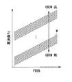
図2は、発振回路15の周波数制御特性を表すものである。図2において、横軸は、周波数制御ワードFBINの値を示し、縦軸は、クロック信号DCOCLK,DCOCLKBの周波数foを示す。図2では、複数(この例では128)の制御特性Wを示している。発振回路15は、周波数制御ワードCBINの値に応じて、複数の周波数制御特性Wのうちの1つを選択する。この例では、周波数制御ワードCBINの値が低いほど周波数foは低く、周波数制御ワードCBINの値が高いほど周波数foは高い。また、発振回路15は、周波数制御ワードFBINの値に応じて、クロック信号DCOCLK,DCOCLKBの周波数foを変化させる。この例では、周波数制御ワードFBINの値が低いほど周波数foは低く、周波数制御ワードFBINの値が高いほど周波数foは高い。図2に示したように、周波数制御ワードCBINを変化させたときの周波数foの変化量は、周波数制御ワードFBINを変化させたときの周波数foの変化量よりも大きい。このようにして、発振回路15では、周波数制御ワードCBINにより周波数foの粗調整を行い、周波数制御ワードFBINにより周波数foの微調整を行うようになっている。
FIG. 2 shows the frequency control characteristics of the
位相検出回路16は、クロック信号DCOCLK,DCOCLKB、基準クロック信号REFCLK、およびクロック信号CLKに基づいて、位相ワードPW2を生成するものである。具体的には、位相検出回路16は、クロック信号DCOCLK,DCOCLKBにより構成される差動信号の位相を固定小数点フォーマットの値として求め、その値を、位相ワードPW2として、クロック信号CLKに基づくタイミングで出力するようになっている。
The
リタイミング回路17は、基準クロック信号REFCLKをクロック信号DCOCLK,DCOCLKBに基づくタイミングでリタイミングして、クロック信号CLKとして出力するものである。
The
この構成により、周波数シンセサイザ1では、クロック信号DCOCLK,DCOCLKBの周波数foが、基準クロック信号REFCLKの周波数と分周比ワードFCWが示す値との積(目標周波数ftarget)になるように負帰還制御される。すなわち、例えば、周波数foが目標周波数ftargetよりも高い場合には、位相ワードPW2が示す値が、基準位相ワードPW1が示す値よりも大きくなり、位相誤差ワードPEWが示す値が小さくなるため、発振回路15は周波数foを低下させる。また、例えば、周波数foが目標周波数ftargetよりも低い場合には、位相ワードPW2が示す値が、基準位相ワードPW1が示す値より小さくなり、位相誤差ワードPEWが示す値が大きくなるため、発振回路15は周波数foを上昇させる。このようにして、周波数シンセサイザ1では、クロック信号DCOCLK,DCOCLKBの周波数foが目標周波数ftargetになるように、負帰還制御されるようになっている。
With this configuration, the
その際、周波数シンセサイザ1は、この例では、2段階で負帰還制御するようになっている。具体的には、周波数シンセサイザ1は、例えば、電源投入直後などの初期状態では、微調整用の周波数制御ワードFBINを所定値に固定し、粗調整用の周波数制御ワードCBINを変化させて負帰還動作を行うことにより、周波数foを目標周波数ftargetに近付ける。そして、その後に、周波数シンセサイザ1は、粗調整用の周波数制御ワードCBINを固定し、微調整用の周波数制御ワードFBINを変化させて負帰還動作を行うことにより、周波数foを目標周波数ftargetにより近付け、位相同期状態を実現するようになっている。
At this time, the
(発振回路15)
図3は、発振回路15の一構成例を表すものである。発振回路15は、制御部20と、発振部30とを有している。
(Oscillation circuit 15)
FIG. 3 illustrates a configuration example of the
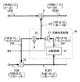
制御部20は、周波数制御ワードCBIN,FBINおよびクロック信号CLKに基づいて、周波数制御ワードCBIN,FBINを、サーモメータコードを示す周波数制御ワードCTM,FTMに変換し、この周波数制御ワードCTM,FTM用いて発振部30を制御するものである。周波数制御ワードCTMは、周波数を粗調整するためのワードであり、128ビット(CTM[127:0])からなるサーモメータコードを示すものである。また、周波数制御ワードFTMは、周波数を微調整するためのワードであり、この例では、64ビット(FTM[63:0])からなるサーモメータコードを示すものである。この制御部20は、後述するように、周波数制御ワードFBINが示す値に基づいて、周波数制御ワードFBINが示す値が取りうる範囲(この例では−512〜+511)より狭い範囲(この例では0〜63)の値を示す周波数制御ワードFTMを生成するとともに、周波数制御ワードFBIN,CBINに基づいて周波数制御ワードCTMを生成するようになっている。
Based on the frequency control words CBIN and FBIN and the clock signal CLK, the
図4は、制御部20の一構成例を表すものである。制御部20は、加算回路21と、リミッタ22と、エンコーダ23と、フリップフロップ24と、減算回路25と、リミッタ26と、符号変換回路27と、エンコーダ28と、フリップフロップ29と、制御回路40とを有している。加算回路21、リミッタ22、エンコード23、およびフリップフロップ24は、粗調整用の周波数制御ワードCBINに係るものであり、減算回路25、リミッタ26、符号変換回路27、エンコーダ28、およびフリップフロップ29は、微調整用の周波数制御ワードFBINに係るものである。
FIG. 4 illustrates a configuration example of the
加算回路21は、粗調整用の周波数制御ワードCBINが示す値と補正ワードCCFが示す値を加算して、その加算結果を示す周波数制御ワードCBIN2を生成するものである。補正ワードCCFは、この例では、7ビット(CCF[6:0])からなるバイナリーフォーマットのワードであり、符号付き数値(−64〜+63)を示すものである。また、周波数制御ワードCBIN2は、この例では、8ビット(CBIN2[7:0])からなるバイナリーフォーマットのワードであり、符号なし数値(0〜255)を示すものである。この周波数制御ワードCBIN2の値は、リミッタ22により規定される範囲の範囲内(この例では0〜127の範囲内)に収まるように動作するようになっている。
The
リミッタ22は、周波数制御ワードCBIN2が示す値が所定の範囲外である場合に、その値をその所定の範囲の下限値または上限値に制限することにより、周波数制御ワードCLMTを生成するものである。この例では、上限値は“127”であり、下限値は“0”である。周波数制御ワードCLMTは、この例では、7ビット(CLMT[6:0])からなるバイナリーフォーマットのワードであり、符号なし数値(0〜127)を示すものである。
The
エンコーダ23は、周波数制御ワードCLMTに基づいてサーモメータコードを生成するものである。フリップフロップ24は、エンコーダ23が生成したサーモメータコードをクロック信号CLKに基づくタイミングでリタイミングして、周波数制御ワードCTM(CTM[127:0])として出力するものである。これにより、周波数制御ワードCTMでは、例えば、最下位ビットCTM[0]から順
The
減算回路25は、微調整用の周波数制御ワードFBINが示す値から補正ワードFCFが示す値を減算して、その減算結果を示す周波数制御ワードFLMT1を生成するものである。補正ワードFCFは、この例では、10ビット(FCF[9:0])からなるバイナリーフォーマットのワードであり、符号付き数値(−512〜+511)を示すものである。また、周波数制御ワードFLMT1は、この例では、10ビット(FLMT1[9:0])からなるバイナリーフォーマットのワードであり、符号付き数値(−512〜+511)を示すものである。後述するように、周波数制御ワードFLMT1の値は、リミッタ26により規定される範囲Rlimの範囲内(この例では−32〜+31の範囲内)に収まるように制御されるようになっている。
The
リミッタ26は、周波数制御ワードFLMT1が示す値が所定の範囲Rlimの範囲外である場合に、その値をその所定の範囲Rlimの下限値または上限値に制限することにより、周波数制御ワードFLMT2を生成するものである。この例では、上限値は“+31”であり、下限値は“−32”である。周波数制御ワードFLMT2は、この例では、6ビット(FLMT2[5:0])からなるバイナリーフォーマットのワードであり、符号付き数値(−32〜+31)を示すものである。
When the value indicated by the frequency control word FLMT1 is outside the range of the predetermined range Rlim, the
符号変換回路27は、符号付き数値を示す周波数制御ワードFLMT2を、符号なし数値を示す周波数制御ワードFUに変換するものである。周波数制御ワードFUは、この例では、6ビット(FU[5:0])からなるバイナリーフォーマットのワードであり、符号なし数値(0〜63)を示すものである。
The
エンコーダ28は、周波数制御ワードFUに基づいてサーモメータコードを生成するものである。フリップフロップ29は、エンコーダ28が生成したサーモメータコードをクロック信号CLKに基づくタイミングでリタイミングして、周波数制御ワードFTMとして出力するものである。これにより、周波数制御ワードFTMでは、例えば、最下位ビットFTM[0]から順に、周波数制御ワードFUが示す値と同じ数だけ“1”が現れるようになっている。
The
制御回路40は、周波数制御ワードFLMT1およびクロック信号CLKに基づいて、補正ワードCCF,FCFを生成するものである。具体的には、制御回路40は、周波数制御ワードFLMT1の値がリミッタ26により規定される範囲Rlimの範囲内(この例では−32〜+31の範囲内)に収まるように、補正ワードFCFを生成するともに、その補正ワードFCFに対応する補正ワードCCFを生成するようになっている。
The
図5は、制御回路40の一構成例を表すものである。この図5では、制御回路40に加え、加算回路21および減算回路25をも示している。制御回路40は、比較回路41と、累積加算回路42と、乗算回路43とを有している。
FIG. 5 illustrates a configuration example of the
比較回路41は、周波数制御ワードFLMT1が示す値と、複数の所定のしきい値とを比較して、比較結果を比較結果ワードOVFとして出力するものである。比較結果ワードOVFは、この例では、10ビット(OVF[9:0])からなるバイナリーフォーマットのワードであり、符号付き数値(−512〜+511)を示すものである。
The
図6は、比較回路41の動作の一例を表すものである。図6には、リミッタ26により規定される範囲Rlimについても併せて示している。比較回路41は、周波数制御ワードFLMT1が示す値と、複数のしきい値TH1,TH2,TH3,…および複数のしきい値TL1,TL2,TL3,…とを比較する。この例では、しきい値TH1は“23”であり、しきい値TH2は“31”であり、しきい値TH3は“39”であり、しきい値TL1は“−24”であり、しきい値TL2は“−32”であり、しきい値TL3は“−40”である。すなわち、この例では、しきい値TH2は範囲Rlimの上限値と等しく、しきい値TL2は範囲Rlimの下限値と等しい。そして、比較回路41は、周波数制御ワードFLMT1が示す値が、しきい値TL1以上でありかつしきい値TH1以下である場合には“0”を示す比較結果ワードOVFを生成する。また、周波数制御ワードFLMT1が示す値が、しきい値TH1より大きくかつしきい値TH2以下である場合には“1”を示す比較結果ワードOVFを生成し、しきい値TH2より大きくかつしきい値TH3以下である場合には“2”を示す比較結果ワードOVFを生成する。周波数制御ワードFLMT1が示す値がさらに大きい場合についても同様である。また、周波数制御ワードFLMT1が示す値が、しきい値TL2以上でありかつしきい値TL1より小さい場合には“−1”を示す比較結果ワードOVFを生成し、しきい値TL3以上でありかつしきい値TL2より小さい場合には“−2”を示す比較結果ワードOVFを生成する。周波数制御ワードFLMT1が示す値がさらに小さい場合についても同様である。
FIG. 6 illustrates an example of the operation of the
累積加算回路42は、比較結果ワードOVFが示す値を累積加算し、その累積加算結果を補正ワードCCFとして出力するものである。
The
乗算回路43は、補正ワードCCFが示す値に所定数(この例では“8”)を乗算し、その乗算結果を補正ワードFCFとして出力するものである。この例では、乗算回路43は、補正ワードCCFを3ビット分シフトすることにより、”8”を乗ずる演算を実現している。この乗算値“8”は、後述するように、粗調整用の可変容量バンク33における各可変容量素子グループ36内の可変容量素子35の数に対応するものである。
The
この構成により、制御部20では、例えば、周波数制御ワードFLMT1がしきい値TH1より大きい値を示す場合には、比較結果ワードOVFが示す値が大きくなり、補正ワードFCFが示す値もまた大きくなるため、減算回路25は周波数制御ワードFLMT1が示す値を小さくする。また、例えば、周波数制御ワードFLMT1がしきい値TL1より小さい値を示す場合には、比較結果ワードOVFが示す値が小さくなり、補正ワードFCFが示す値もまた小さくなるため、減算回路25は周波数制御ワードFLMT1が示す値を大きくする。このようにして、制御部20では、周波数制御ワードFLMT1の値がリミッタ26により規定される範囲Rlimの範囲内(この例では−32〜+31の範囲内)に収まるように、負帰還制御されるようになっている。
With this configuration, in the
発振部30は、図3に示したように、周波数制御ワードCTM,FTMに基づいて、周波数制御ワードCTM,FTMに応じた周波数foのクロック信号DCOCLK,DCOCLKBを生成するものである。
As shown in FIG. 3, the oscillating
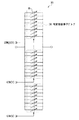
図7は、発振部30の一構成例を表すものである。発振部30は、負性抵抗31と、インダクタ32と、可変容量バンク33,34とを有している。
FIG. 7 illustrates a configuration example of the
負性抵抗31は、トランジスタなどの能動素子を含んで構成されるものであり、一端と他端との間の抵抗値が負の極性をもつようにふるまうものである。負性抵抗31の一端は、インダクタ32の一端および可変容量バンク33,34の一端などに接続されるとともに、他端は、インダクタ32の他端および可変容量バンク33,34の他端などに接続されている。
The
インダクタ32の一端は、可変容量バンク33,34の一端および負性抵抗31の一端などに接続され、他端は、可変容量バンク33,34の他端および負性抵抗31の他端などに接続されている。
One end of the
可変容量バンク33は、粗調整用の周波数制御ワードCTMに基づいて両端間のキャパシタンスが変化するものである。可変容量バンク33の一端は、インダクタ32の一端、可変容量バンク34の一端、および負性抵抗31の一端に接続されている。
The
図8は、可変容量バンク33の一構成例を表すものである。可変容量バンク33は、この例では、128個の可変容量素子グループ36を有している。各可変容量素子グループ36は、周波数制御ワードCTMのビットCTM[127:0]のそれぞれと対応して設けられている。各可変容量素子グループ36は、この例では、8つの可変容量素子35を有している。この可変容量素子35の数“8”は、乗算回路43における乗算値“8”に対応するものである。可変容量素子35は、容量制御端子に印加された電圧に基づいて両端間のキャパシタンスが変化するものである。これらの8つの可変容量素子35は、互いに並列接続されるとともに、容量制御端子も互いに接続されている。これにより可変容量素子グループ36は、可変容量素子35の8倍のキャパシタンスを有する可変容量素子として機能するようになっている。可変容量素子グループ36の8つの可変容量素子35の容量制御端子には、周波数制御ワードCTMの対応するビットに基づいて電圧が印加され、その印加された電圧に基づいて、可変容量素子グループ36の両端間のキャパシタンスが変化するようになっている。これらの可変容量素子グループ36は、互いに並列接続されている。この構成により、可変容量バンク33では、周波数制御ワードCTMに基づいて両端間のキャパシタンスが変化するようになっている。
FIG. 8 illustrates a configuration example of the
可変容量バンク34は、微調整用の周波数制御ワードFTMに基づいて両端間のキャパシタンスが変化するものである。可変容量バンク34の一端は、インダクタ32の一端、可変容量バンク33の一端、および負性抵抗31の一端に接続されている。
In the
図9は、可変容量バンク34の一構成例を表すものである。可変容量バンク34は、この例では、64個の可変容量素子35を有している。各可変容量素子35は、周波数制御ワードFTMのビットFTM[63:0]のそれぞれと対応して設けられている。可変容量素子35の容量制御端子には、周波数制御ワードFTMの対応するビットに基づいて電圧が印加され、その印加された電圧に基づいて、可変容量素子35の両端間のキャパシタンスが変化するようになっている。これらの可変容量素子35は、互いに並列接続されている。この構成により、可変容量バンク34では、周波数制御ワードFTMに基づいて両端間のキャパシタンスが変化するようになっている。
FIG. 9 illustrates a configuration example of the
可変容量バンク33と可変容量バンク34とでは、周波数制御ワードCTM,FTMのうちのビットが1つ変化したときの両端間のキャパシタンスの変化量が異なる。すなわち、この例では、周波数制御ワードCTMのビットが1つ変化することによる可変容量バンク33の両端間のキャパシタンスの変化量は、周波数制御ワードFTMのビットが1つ変化することによる可変容量バンク34の両端間のキャパシタンスの変化量の8倍になっている。
The
この構成により、発振部30は、インダクタ32のインダクタンス、および可変容量バンク33,34のキャパシタンスによって画定される共振周波数(周波数fo)で発振動作を行い、クロック信号DCOCLK,DCOCLKBを生成する。その際、周波数制御ワードCTMを変化させたときの周波数foの変化量は、周波数制御ワードFTMを変化させたときの周波数foの変化量よりも大きくなる。これにより、発振部30では、周波数制御ワードCTMに基づいて周波数foの粗調整を行うとともに、周波数制御ワードFTMに基づいて周波数foの微調整を行うことができるようになっている。
With this configuration, the oscillating
ここで、発振回路15は、本開示における「発振回路」の一具体例に対応する。制御回路40、加算回路21、および減算回路25は、本開示における「演算部」の一具体例に対応する。周波数制御ワードFBINの値は、本開示における「第1の入力コード値」の一具体例に対応し、周波数制御ワードCBINの値は、本開示における「第2の入力コード値」の一具体例に対応する。周波数制御ワードFLMT1の値は、本開示における「第1のコード値」の一具体例に対応し、周波数制御ワードCBIN2の値は、本開示における「第2のコード値」の一具体例に対応する。
Here, the
[動作および作用]
続いて、本実施の形態の周波数シンセサイザ1の動作および作用について説明する。
[Operation and Action]
Next, the operation and action of the
(全体動作概要)
まず、図1,3,4などを参照して、周波数シンセサイザ1の全体動作概要を説明する。基準位相生成回路11は、分周比ワードFCWおよびクロック信号CLKに基づいて、基準位相ワードPW1を生成する。位相比較回路12は、基準位相ワードPW1および位相ワードPW2に基づいて、位相誤差ワードPEWを生成する。ループフィルタ13は、位相誤差ワードPEWおよびクロック信号CLKに基づいて、位相誤差ワードPEW2を生成する。利得調整回路14は、位相誤差ワードPEW2に基づいて、周波数制御ワードCBIN,FBINを生成する。発振回路15は、周波数制御ワードCBIN,FBINおよびクロック信号CLKに基づいて、クロック信号DCOCLK,DCOCLKBを生成する。具体的には、発振回路15では、制御部20が、周波数制御ワードCBIN,FBINおよびクロック信号CLKに基づいて、周波数制御ワードCBIN,FBINを周波数制御ワードCTM,FTMに変換し、発振部30が、周波数制御ワードCTM,FTMに基づいて、周波数制御ワードCTM,FTMに応じた周波数foのクロック信号DCOCLK,DCOCLKBを生成する。位相検出回路16は、クロック信号DCOCLK,DCOCLKB、基準クロック信号REFCLK、およびクロック信号CLKに基づいて、位相ワードPW2を生成する。リタイミング回路17は、基準クロック信号REFCLKをクロック信号DCOCLK,DCOCLKBに基づくタイミングでリタイミングして、クロック信号CLKとして出力する。
(Overview of overall operation)
First, an overall operation outline of the
制御部20では、加算回路21が、周波数制御ワードCBINが示す値と補正ワードCCFが示す値を加算して、その加算結果を示す周波数制御ワードCBIN2を生成する。リミッタ22は、周波数制御ワードCBIN2が示す値が所定の範囲外である場合に、その値をその所定の範囲の下限値または上限値に制限することにより、周波数制御ワードCLMTを生成する。エンコーダ23は、周波数制御ワードCLMTに基づいてサーモメータコードを生成する。フリップフロップ24は、エンコーダ23が生成したサーモメータコードをクロック信号CLKに基づくタイミングでリタイミングして、周波数制御ワードCTMとして出力する。
In the
減算回路25は、周波数制御ワードFBINが示す値から補正ワードFCFが示す値を減算して、その減算結果を示す周波数制御ワードFLMT1を生成する。制御回路40は、周波数制御ワードFLMT1およびクロック信号CLKに基づいて、補正ワードCCF,FCFを生成する。リミッタ26は、周波数制御ワードFLMT1が示す値が所定の範囲Rlimの範囲外である場合に、その値をその所定の範囲Rlimの下限値または上限値に制限することにより、周波数制御ワードFLMT2を生成する。符号変換回路27は、符号付き数値を示す周波数制御ワードFLMT2を、符号なし数値を示す周波数制御ワードFUに変換する。エンコーダ28は、周波数制御ワードFUに基づいてサーモメータコードを生成する。フリップフロップ29は、エンコーダ28が生成したサーモメータコードをクロック信号CLKに基づくタイミングでリタイミングして、周波数制御ワードFTMとして出力する。
The
(詳細動作)
次に、周波数シンセサイザ1の詳細動作について説明する。周波数シンセサイザ1は、例えば、電源投入直後などの初期状態では、微調整用の周波数制御ワードFBINを所定の値(例えば“0”)に固定し、粗調整用の周波数制御ワードCBINを変化させることにより負帰還動作を行う。その際、補正ワードCCF,FCFが示す値は“0”を維持するため、制御部20は、粗調整用の周波数制御ワードCBINが示す値をサーモメータコードに変換することにより周波数制御ワードCTMを生成する。そして、周波数シンセサイザ1は、この負帰還動作により、周波数foを目標周波数ftargetに近付ける(動作P1)。
(Detailed operation)
Next, detailed operation of the
そして、その後に、周波数シンセサイザ1は、粗調整用の周波数制御ワードCBINを固定し、微調整用の周波数ワードFBINを変化させることにより負帰還動作を行う。その際、制御回路40は、周波数制御ワードFLMT1の値が範囲Rlimの範囲内(この例では−32〜+31の範囲内)に収まるように、補正ワードFCFを生成するともに、その補正ワードFCFに対応する補正ワードCCFを生成する。そして、周波数シンセサイザ1は、この負帰還動作により、周波数foを目標周波数ftargetにより近付け、位相同期状態を実現する(動作P2)。
After that, the
以下に、この動作P2について、詳細に説明する。まず最初に、周波数制御ワードFLMT1が範囲Rlimの上限値付近の値を示す場合における動作を説明し、次に、周波数制御ワードFLMT1が範囲Rlimの下限値付近の値を示す場合における動作を説明する Hereinafter, the operation P2 will be described in detail. First, an operation when the frequency control word FLMT1 indicates a value near the upper limit value of the range Rlim will be described. Next, an operation when the frequency control word FLMT1 indicates a value near the lower limit value of the range Rlim will be described.
図10は、周波数制御ワードFLMT1が範囲Rlimの上限値付近の値を示す場合における、発振回路15の動作のタイミング図を表すものであり、(A)はクロック信号CLKの波形を示し、(B)は周波数制御ワードFBINを示し、(C)は周波数制御ワードFLMT1を示し、(D)は比較結果ワードOVFを示し、(E)は補正ワードCCFを示し、(F)は補正ワードFCFを示し、(G)は周波数制御ワードCBINを示し、(H)は周波数制御ワードCBIN2を示し、(I)は周波数制御ワードFTMを示す。この例では、粗調整用の周波数制御ワードCBINは“64”に固定され、周波数制御ワードFBINが過渡的に変化している。これにより、発振回路15の状態が、状態S1〜S7のように変化している。
FIG. 10 shows a timing chart of the operation of the
図11は、図10に示した状態S1〜S7を、発振部30の周波数制御特性を用いて表すものである。この図11では、横軸は周波数制御ワードFLMT1の値を示し、縦軸は周波数foを示している。
FIG. 11 illustrates the states S1 to S7 illustrated in FIG. 10 using the frequency control characteristics of the
状態S1において、粗調整用の周波数制御ワードCBINの値は“64”であり(図10(G))、微調整用の周波数制御ワードFBINの値は“20”である(図10(B))。また、補正ワードCCFの値が“0”であるため(図10(E))、加算回路21は、周波数制御ワードCBIN2の値を“64”(=64+0)にし(図10(H))、その結果、制御部20は、粗調整用の周波数制御ワードCTMの値を“64”にする。同様に、補正ワードFCFの値が“0”であるため(図10(F))、減算回路25は、周波数制御ワードFLMT1の値を“20”(=20+0)にし(図10(C))、その結果、制御部20は、微調整用の周波数制御ワードFTMの値を“52”(=20+32)にする(図10(I))。この周波数制御ワードFLMT1の値“20”は、しきい値TL1(−24)以上でありかつしきい値TH1(23)以下であるため、比較回路41は、比較結果ワードOVFの値を“0”にする(図10(D))。
In the state S1, the value of the frequency control word CBIN for coarse adjustment is “64” (FIG. 10G), and the value of the frequency control word FBIN for fine adjustment is “20” (FIG. 10B). ). Since the value of the correction word CCF is “0” (FIG. 10E), the
このようにして、状態S1では、図11に示したように、粗調整用の周波数制御ワードCTMの値“64”(CTM=64)に対応した周波数制御特性が選択され、発振部30は、周波数制御ワードFLMT1の値“20”に応じた周波数foで発振する。 In this manner, in the state S1, as shown in FIG. 11, the frequency control characteristic corresponding to the value “64” (CTM = 64) of the frequency control word CTM for coarse adjustment is selected. It oscillates at a frequency fo corresponding to the value “20” of the frequency control word FLMT1.
次に、状態S2において、微調整用の周波数制御ワードFBINの値が“25”に変化する(図10(B))。また、一つ前の状態S1において、比較結果ワードOVFの値が“0”であったため、累積加算回路42および乗算回路43は、補正ワードCCF,FCFの値をともに”0”にする(図10(E),(F))。これにより、加算回路21は、周波数制御ワードCBIN2の値を“64”(=64+0)にし(図10(H))、その結果、制御部20は、粗調整用の周波数制御ワードCTMの値を“64”にする。減算回路25は、周波数制御ワードFLMT1の値を“25”(=25+0)にし(図10(C))、その結果、制御部20は、微調整用の周波数制御ワードFTMの値を“57”(=25+32)にする(図10(I))。この周波数制御ワードFLMT1の値“25”は、しきい値TH1(=23)より大きくかつしきい値TH2(31)以下であるため、比較回路41は、比較結果ワードOVFの値を“1”にする(図10(D))。
Next, in the state S2, the value of the frequency control word FBIN for fine adjustment changes to “25” (FIG. 10B). Further, in the previous state S1, since the value of the comparison result word OVF is “0”, the
このようにして、状態S2では、図11に示したように、粗調整用の周波数制御ワードCTMの値“64”(CTM=64)に対応した周波数制御特性が引き続き選択され、発振部30は、周波数制御ワードFLMT1の値“25”に応じた周波数foで発振する。
In this manner, in the state S2, as shown in FIG. 11, the frequency control characteristic corresponding to the value “64” (CTM = 64) of the frequency control word CTM for coarse adjustment is continuously selected, and the
次に、状態S3において、微調整用の周波数制御ワードFBINの値が“30”に変化する(図10(B))。また、一つ前の状態S2において、比較結果ワードOVFの値が“1”であったため、累積加算回路42は、補正ワードCCFの値を“1”にするとともに(図10(E))、乗算回路43は、補正ワードFCFの値を“8”にする(図10(F))。これにより、加算回路21は、周波数制御ワードCBIN2の値を“65”(=64+1)にし(図10(H))、その結果、制御部20は、粗調整用の周波数制御ワードCTMの値を“65”にする。また、減算回路25は、周波数制御ワードFLMT1の値を“22”(=30−8)にし(図10(C))、その結果、制御部20は、微調整用の周波数制御ワードFTMの値を“54”(=22+32)にする(図10(I))。この周波数制御ワードFLMT1の値“22”は、しきい値TL1(−24)以上でありかつしきい値TH1(23)以下であるため、比較回路41は、比較結果ワードOVFの値を“0”にする(図10(D))。
Next, in the state S3, the value of the frequency control word FBIN for fine adjustment changes to “30” (FIG. 10B). Further, in the previous state S2, since the value of the comparison result word OVF is “1”, the
このようにして、状態S3では、図11に示したように、粗調整用の周波数制御ワードCTMの値“65”(CTM=65)に対応した周波数制御特性が選択され、発振部30は、周波数制御ワードFLMT1の値“22”に応じた周波数foで発振する。
In this way, in the state S3, as shown in FIG. 11, the frequency control characteristic corresponding to the value “65” (CTM = 65) of the frequency control word CTM for coarse adjustment is selected, and the
次に、状態S4において、微調整用の周波数制御ワードFBINの値が“37”に変化する(図10(B))。また、一つ前の状態S3において、比較結果ワードOVFの値が“0”であったため、累積加算回路42は、補正ワードCCFの値“1”を維持するとともに(図10(E))、乗算回路43は、補正ワードFCFの値“8”を維持する(図10(F))。これにより、加算回路21は、周波数制御ワードCBIN2の値を“65”(=64+1)にし(図10(H))、その結果、制御部20は、粗調整用の周波数制御ワードCTMの値を“65”にする。また、減算回路25は、周波数制御ワードFLMT1の値を“29”(=37−8)にし(図10(C))、その結果、制御部20は、微調整用の周波数制御ワードFTMの値を“61”(=29+32)にする(図10(I))。この周波数制御ワードFLMT1の値“29”は、しきい値TH1(23)より大きくかつしきい値TH2(31)以下であるため、比較回路41は、比較結果ワードOVFの値を“1”にする(図10(D))。
Next, in the state S4, the value of the frequency control word FBIN for fine adjustment changes to “37” (FIG. 10B). Further, in the previous state S3, since the value of the comparison result word OVF is “0”, the
このようにして、状態S4では、図11に示したように、粗調整用の周波数制御ワードCTMの値“65”(CTM=65)に対応した周波数制御特性が引き続き選択され、発振部30は、周波数制御ワードFLMT1の値“29”に応じた周波数foで発振する。
In this manner, in the state S4, as shown in FIG. 11, the frequency control characteristic corresponding to the value “65” (CTM = 65) of the frequency control word CTM for coarse adjustment is continuously selected, and the
次に、状態S5において、微調整用の周波数制御ワードFBINの値が“42”に変化する(図10(B))。また、一つ前の状態S4において、比較結果ワードOVFの値が“1”であったため、累積加算回路42は、補正ワードCCFの値を“2”にするとともに(図10(E))、乗算回路43は、補正ワードFCFの値を“16”にする(図10(F))。これにより、加算回路21は、周波数制御ワードCBIN2の値を“66”(=64+2)にし(図10(H))、その結果、制御部20は、粗調整用の周波数制御ワードCTMの値を“66”にする。また、減算回路25は、周波数制御ワードFLMT1の値を“26”(=42−16)にし(図10(C))、その結果、制御部20は、微調整用の周波数制御ワードFTMの値を“58”(=26+32)にする(図10(I))。この周波数制御ワードFLMT1の値“26”は、しきい値TH1(23)より大きくかつしきい値TH2(31)以下であるため、比較回路41は、比較結果ワードOVFの値を“1”にする(図10(D))。
Next, in the state S5, the value of the frequency control word FBIN for fine adjustment changes to “42” (FIG. 10B). In the previous state S4, since the value of the comparison result word OVF is “1”, the
このようにして、状態S5では、図11に示したように、粗調整用の周波数制御ワードCTMの値“66”(CTM=66)に対応した周波数制御特性が選択され、発振部30は、周波数制御ワードFLMT1の値“26”に応じた周波数foで発振する。
Thus, in the state S5, as shown in FIG. 11, the frequency control characteristic corresponding to the value “66” (CTM = 66) of the frequency control word CTM for coarse adjustment is selected, and the
次に、状態S6において、微調整用の周波数制御ワードFBINの値が“44”に変化する(図10(B))。また、一つ前の状態S5において、比較結果ワードOVFの値が“1”であったため、累積加算回路42は、補正ワードCCFの値を“3”にするとともに(図10(E))、乗算回路43は、補正ワードFCFの値を“24”にする(図10(F))。これにより、加算回路21は、周波数制御ワードCBIN2の値を“67”(=64+3)にし(図10(H))、その結果、制御部20は、粗調整用の周波数制御ワードCTMの値を“67”にする。また、減算回路25は、周波数制御ワードFLMT1の値を“20”(=44−24)にし(図10(C))、その結果、制御部20は、微調整用の周波数制御ワードFTMの値を“52”(=20+32)にする(図10(I))。この周波数制御ワードFLMT1の値“20”は、しきい値TL1(−24)以上でありかつしきい値TH1(23)以下であるため、比較回路41は、比較結果ワードOVFの値を“0”にする(図10(D))。
Next, in the state S6, the value of the frequency control word FBIN for fine adjustment changes to “44” (FIG. 10B). Further, in the previous state S5, since the value of the comparison result word OVF is “1”, the
このようにして、状態S6では、図11に示したように、粗調整用の周波数制御ワードCTMの値“67”(CTM=67)に対応した周波数制御特性が選択され、発振部30は、周波数制御ワードFLMT1の値“20”に応じた周波数foで発振する。 In this way, in the state S6, as shown in FIG. 11, the frequency control characteristic corresponding to the value “67” (CTM = 67) of the frequency control word CTM for coarse adjustment is selected. It oscillates at a frequency fo corresponding to the value “20” of the frequency control word FLMT1.
次に、状態S7において、微調整用の周波数制御ワードFBINの値が“40”に変化する(図10(B))。また、一つ前の状態S6において、比較結果ワードOVFの値が“0”であったため、累積加算回路42は、補正ワードCCFの値“3”を維持するとともに(図10(E))、乗算回路43は、補正ワードFCFの値“24”を維持する(図10(F))。これにより、加算回路21は、周波数制御ワードCBIN2の値を“67”(=64+3)にし(図10(H))、その結果、制御部20は、粗調整用の周波数制御ワードCTMの値を“67”にする。また、減算回路25は、周波数制御ワードFLMT1の値を“16”(=40−24)にし(図10(C))、その結果、制御部20は、微調整用の周波数制御ワードFTMの値を“48”(=16+32)にする(図10(I))。この周波数制御ワードFLMT1の値“16”は、しきい値TL1(−24)以上でありかつしきい値TH1(23)以下であるため、比較回路41は、比較結果ワードOVFの値を“0”にする(図10(D))。
Next, in the state S7, the value of the frequency control word FBIN for fine adjustment changes to “40” (FIG. 10B). Further, in the previous state S6, since the value of the comparison result word OVF is “0”, the
このようにして、状態S7では、図11に示したように、粗調整用の周波数制御ワードCTMの値“67”(CTM=67)に対応した周波数制御特性が引き続き選択され、発振部30は、周波数制御ワードFLMT1の値“16”に応じた周波数foで発振する。
In this manner, in the state S7, as shown in FIG. 11, the frequency control characteristic corresponding to the value “67” (CTM = 67) of the frequency control word CTM for coarse adjustment is continuously selected, and the
図12は、周波数制御ワードFLMT1が範囲Rlimの下限値付近の値を示す場合における、発振回路15の動作のタイミング図を表すものであり、(A)はクロック信号CLKの波形を示し、(B)は周波数制御ワードFBINを示し、(C)は周波数制御ワードFLMT1を示し、(D)は比較結果ワードOVFを示し、(E)は補正ワードCCFを示し、(F)は補正ワードFCFを示し、(G)は周波数制御ワードCBINを示し、(H)は周波数制御ワードCBIN2を示し、(I)は周波数制御ワードFTMを示す。この例では、粗調整用の周波数制御ワードCBINは“64”に固定され、周波数制御ワードFBINが過渡的に変化している。これにより、発振回路15の状態が、状態S11〜S17のように変化している。
FIG. 12 shows a timing chart of the operation of the
図13は、図12に示した状態S11〜S17を、発振部30の周波数制御特性を用いて表すものである。
FIG. 13 illustrates the states S11 to S17 illustrated in FIG. 12 using the frequency control characteristics of the
状態S11において、粗調整用の周波数制御ワードCBINの値は“64”であり(図12(G))、微調整用の周波数制御ワードFBINの値は“−19”である(図12(B))。また、補正ワードCCFの値が“0”であるため(図12(E))、加算回路21は、周波数制御ワードCBIN2の値を“64”(=64+0)にし(図12(H))、その結果、制御部20は、粗調整用の周波数制御ワードCTMの値を“64”にする。同様に、補正ワードFCFの値が“0”であるため(図12(F))、減算回路25は、周波数制御ワードFLMT1の値を“−19”(=−19+0)にし(図12(C))、その結果、制御部20は、微調整用の周波数制御ワードFTMの値を“13”(=−19+32)にする(図12(I))。この周波数制御ワードFLMT1の値“−19”は、しきい値TL1(−24)以上でありかつしきい値TH1(23)以下であるため、比較回路41は、比較結果ワードOVFの値を“0”にする(図12(D))。
In the state S11, the value of the frequency control word CBIN for coarse adjustment is “64” (FIG. 12G), and the value of the frequency control word FBIN for fine adjustment is “−19” (FIG. 12B )). Since the value of the correction word CCF is “0” (FIG. 12E), the adding
このようにして、状態S11では、図13に示したように、粗調整用の周波数制御ワードCTMの値“64”(CTM=64)に対応した周波数制御特性が選択され、発振部30は、周波数制御ワードFLMT1の値“−19”に応じた周波数foで発振する。 In this manner, in the state S11, as shown in FIG. 13, the frequency control characteristic corresponding to the value “64” (CTM = 64) of the frequency control word CTM for coarse adjustment is selected. It oscillates at a frequency fo corresponding to the value “−19” of the frequency control word FLMT1.
次に、状態S12において、微調整用の周波数制御ワードFBINの値が“−29”に変化する(図12(B))。また、一つ前の状態S11において、比較結果ワードOVFの値が“0”であったため、累積加算回路42および乗算回路43は、補正ワードCCF,FCFの値をともに”0”にする(図12(E),(F))。これにより、加算回路21は、周波数制御ワードCBIN2の値を“64”(=64+0)にし(図12(H))、その結果、制御部20は、粗調整用の周波数制御ワードCTMの値を“64”にする。減算回路25は、周波数制御ワードFLMT1の値を“−29”(=−29+0)にし(図12(C))、その結果、制御部20は、微調整用の周波数制御ワードFTMの値を“3”(=−29+32)にする(図12(I))。この周波数制御ワードFLMT1の値“−29”は、しきい値TL2(−32)以上でありかつしきい値TL1(−24)より小さいため、比較回路41は、比較結果ワードOVFの値を“−1”にする(図12(D))。
Next, in the state S12, the value of the frequency control word FBIN for fine adjustment changes to “−29” (FIG. 12B). In addition, since the value of the comparison result word OVF is “0” in the previous state S11, the
このようにして、状態S12では、図13に示したように、粗調整用の周波数制御ワードCTMの値“64”(CTM=64)に対応した周波数制御特性が引き続き選択され、発振部30は、周波数制御ワードFLMT1の値“−29”に応じた周波数foで発振する。
In this manner, in the state S12, as shown in FIG. 13, the frequency control characteristic corresponding to the value “64” (CTM = 64) of the frequency control word CTM for coarse adjustment is continuously selected, and the
次に、状態S13において、微調整用の周波数制御ワードFBINの値が“−33”に変化する(図12(B))。また、一つ前の状態S12において、比較結果ワードOVFの値が“−1”であったため、累積加算回路42は、補正ワードCCFの値を“−1”にするとともに(図12(E))、乗算回路43は、補正ワードFCFの値を“−8”にする(図12(F))。これにより、加算回路21は、周波数制御ワードCBIN2の値を“63”(=64−1)にし(図12(H))、その結果、制御部20は、粗調整用の周波数制御ワードCTMの値を“63”にする。また、減算回路25は、周波数制御ワードFLMT1の値を“−25”(=−33+8)にし(図12(C))、その結果、制御部20は、微調整用の周波数制御ワードFTMの値を“7”(=−25+32)にする(図12(I))。この周波数制御ワードFLMT1の値“−25”は、しきい値TL2(−32)以上でありかつしきい値TL1(−24)より小さいため、比較回路41は、比較結果ワードOVFの値を“−1”にする(図12(D))。
Next, in the state S13, the value of the frequency control word FBIN for fine adjustment changes to “−33” (FIG. 12B). In the previous state S12, since the value of the comparison result word OVF is “−1”, the
このようにして、状態S13では、図13に示したように、粗調整用の周波数制御ワードCTMの値“63”(CTM=63)に対応した周波数制御特性が選択され、発振部30は、周波数制御ワードFLMT1の値“−25”に応じた周波数foで発振する。 In this manner, in the state S13, as shown in FIG. 13, the frequency control characteristic corresponding to the value “63” (CTM = 63) of the frequency control word CTM for coarse adjustment is selected. It oscillates at a frequency fo corresponding to the value “−25” of the frequency control word FLMT1.
次に、状態S14において、微調整用の周波数制御ワードFBINの値が“−38”に変化する(図12(B))。また、一つ前の状態S13において、比較結果ワードOVFの値が“−1”であったため、累積加算回路42は、補正ワードCCFの値を“−2”にするとともに(図12(E))、乗算回路43は、補正ワードFCFの値を“−16”にする(図12(F))。これにより、加算回路21は、周波数制御ワードCBIN2の値を“62”(=64−2)にし(図12(H))、その結果、制御部20は、粗調整用の周波数制御ワードCTMの値を“62”にする。また、減算回路25は、周波数制御ワードFLMT1の値を“−22”(=−38+16)にし(図12(C))、その結果、制御部20は、微調整用の周波数制御ワードFTMの値を“10”(=−22+32)にする(図12(I))。この周波数制御ワードFLMT1の値“−22”は、しきい値TL1(−24)以上でありかつしきい値TH1(23)以下であるため、比較回路41は、比較結果ワードOVFの値を“0”にする(図12(D))。
Next, in the state S14, the value of the fine adjustment frequency control word FBIN changes to “−38” (FIG. 12B). In the previous state S13, since the value of the comparison result word OVF is “−1”, the
このようにして、状態S14では、図13に示したように、粗調整用の周波数制御ワードCTMの値“62”(CTM=62)に対応した周波数制御特性が選択され、発振部30は、周波数制御ワードFLMT1の値“−38”に応じた周波数foで発振する。 In this way, in the state S14, as shown in FIG. 13, the frequency control characteristic corresponding to the value “62” (CTM = 62) of the frequency control word CTM for coarse adjustment is selected. It oscillates at a frequency fo corresponding to the value “−38” of the frequency control word FLMT1.
次に、状態S15において、微調整用の周波数制御ワードFBINの値が“−41”に変化する(図12(B))。また、一つ前の状態S14において、比較結果ワードOVFの値が“0”であったため、累積加算回路42は、補正ワードCCFの値“−2”を維持するとともに(図12(E))、乗算回路43は、補正ワードFCFの値“−16”を維持する(図12(F))。これにより、加算回路21は、周波数制御ワードCBIN2の値を“62”(=64−2)にし(図12(H))、その結果、制御部20は、粗調整用の周波数制御ワードCTMの値を“62”にする。また、減算回路25は、周波数制御ワードFLMT1の値を“−25”(=−41+16)にし(図12(C))、その結果、制御部20は、微調整用の周波数制御ワードFTMの値を“7”(=−25+32)にする(図12(I))。この周波数制御ワードFLMT1の値“−25”は、しきい値TL2(−32)以上でありかつしきい値TL1(−24)より小さいため、比較回路41は、比較結果ワードOVFの値を“−1”にする(図12(D))。
Next, in the state S15, the value of the frequency control word FBIN for fine adjustment changes to “−41” (FIG. 12B). Further, in the previous state S14, since the value of the comparison result word OVF was “0”, the
このようにして、状態S15では、図13に示したように、粗調整用の周波数制御ワードCTMの値“62”(CTM=62)に対応した周波数制御特性が引き続き選択され、発振部30は、周波数制御ワードFLMT1の値“−25”に応じた周波数foで発振する。
In this way, in the state S15, as shown in FIG. 13, the frequency control characteristic corresponding to the value “62” (CTM = 62 ) of the frequency control word CTM for coarse adjustment is continuously selected, and the
次に、状態S16において、微調整用の周波数制御ワードFBINの値が“−44”に変化する(図12(B))。また、一つ前の状態S15において、比較結果ワードOVFの値が“−1”であったため、累積加算回路42は、補正ワードCCFの値を“−3”にするとともに(図12(E))、乗算回路43は、補正ワードFCFの値を“−24”にする(図12(F))。これにより、加算回路21は、周波数制御ワードCBIN2の値を“61”(=64−3)にし(図12(H))、その結果、制御部20は、粗調整用の周波数制御ワードCTMの値を“61”にする。また、減算回路25は、周波数制御ワードFLMT1の値を“−20”(=−44+24)にし(図12(C))、その結果、制御部20は、微調整用の周波数制御ワードFTMの値を“12”(=−20+32)にする(図12(I))。この周波数制御ワードFLMT1の値“−20”は、しきい値TL1(−24)以上でありかつしきい値TH1(23)以下であるため、比較回路41は、比較結果ワードOVFの値を“0”にする(図12(D))。
Next, in the state S16, the value of the frequency control word FBIN for fine adjustment changes to “−44” (FIG. 12B). In the previous state S15, since the value of the comparison result word OVF is “−1”, the
このようにして、状態S16では、図13に示したように、粗調整用の周波数制御ワードCTMの値“61”(CTM=61)に対応した周波数制御特性が選択され、発振部30は、周波数制御ワードFLMT1の値“−20”に応じた周波数foで発振する。
In this manner, in the state S16, as shown in FIG. 13, the frequency control characteristic corresponding to the value “61” (CTM = 61) of the frequency control word CTM for coarse adjustment is selected, and the
次に、状態S17において、微調整用の周波数制御ワードFBINの値が“−42”に変化する(図12(B))。また、一つ前の状態S16において、比較結果ワードOVFの値が“0”であったため、累積加算回路42は、補正ワードCCFの値“−3”を維持するとともに(図12(E))、乗算回路43は、補正ワードFCFの値“−24”を維持する(図12(F))。これにより、加算回路21は、周波数制御ワードCBIN2の値を“61”(=64−3)にし(図12(H))、その結果、制御部20は、粗調整用の周波数制御ワードCTMの値を“61”にする。また、減算回路25は、周波数制御ワードFLMT1の値を“−18”(=−42+24)にし(図12(C))、その結果、制御部20は、微調整用の周波数制御ワードFTMの値を“14”(=−18+32)にする(図12(I))。この周波数制御ワードFLMT1の値“−18”は、しきい値TL1(−24)以上でありかつしきい値TH1(23)以下であるため、比較回路41は、比較結果ワードOVFの値を“0”にする(図12(D))。
Next, in the state S17, the value of the frequency control word FBIN for fine adjustment changes to “−42” (FIG. 12B). In the previous state S16, since the value of the comparison result word OVF is “0”, the
このようにして、状態S17では、図13に示したように、粗調整用の周波数制御ワードCTMの値“61”(CTM=61)に対応した周波数制御特性が引き続き選択され、発振部30は、周波数制御ワードFLMT1の値“−18”に応じた周波数foで発振する。
In this manner, in the state S17, as shown in FIG. 13, the frequency control characteristic corresponding to the value “61” (CTM = 61) of the frequency control word CTM for coarse adjustment is continuously selected, and the
発振回路15では、図11に示したように、ある状態において、周波数制御ワードFLMT1の値がしきい値TH1よりも大きくなった場合(例えば状態S2,S4,S5)には、その次の状態において、粗調整用の周波数制御ワードCTMの値を高くし、粗調整用の可変容量バンク33の設定を切り替える。また、同様に、発振回路15では、図13に示したように、ある状態において、周波数制御ワードFLMT1の値がしきい値TL1よりも小さくなった場合(例えば状態S12,S13,S15)には、その次の状態において、粗調整用の周波数制御ワードCTMの値を低くし、粗調整用の可変容量バンク33の設定を切り替える。これにより、周波数制御ワードFLMT1の値を範囲Rlimの範囲内(この例では−32〜+31の範囲内)に収めつつ、周波数制御範囲を広くすることができる。
In the
すなわち、例えば、粗調整用の可変容量バンク33の設定を切り替えない場合には、図11において、状態S3〜S7は状態D3〜D7に示したようになり、図13において、状態S13〜S17は状態D13〜D17に示したようになる。すなわち、この場合、微調整用の周波数制御ワードFLMT1の値をより広い範囲で変化させる必要がある。また、周波数制御範囲の上限近くまたは下限近くで動作させる場合には、周波数制御ワードの値が上限値または下限値を超えてしまい、周波数foが飽和してしまうおそれがある。
That is, for example, when the setting of the
一方、発振回路15では、粗調整用の可変容量バンク33の設定を切り替えるようにしている。これにより、微調整用の周波数制御ワードFLMT1の値を狭い範囲内で変化させつつ、周波数制御範囲を広くすることができ、周波数foが飽和するおそれを低減することができる。
On the other hand, in the
また、発振回路15では、周波数制御ワードFLMT1の値がしきい値TH1よりも大きくなった場合やしきい値TL1よりも小さくなった場合に、粗調整用の可変容量バンク33の設定を切り替えるようにしたので、可変容量バンク33の設定を切り替える頻度を少なくすることができる。
The
すなわち、例えば、図11に示したように、状態S5から状態S6に遷移する場合には、発振回路15では、周波数foを上げる制御が行われ、粗調整用の可変容量バンク33の設定が切り替わる。一方、状態S6から状態S7に遷移する場合には、発振回路15では、周波数foを下げる制御が行われるが、粗調整用の可変容量バンク33の設定は維持されている。すなわち、状態S6では、周波数制御ワードFLMT1の値をしきい値TH1以下に維持したまま、周波数制御ワードCTMの値を大きくすることにより高い周波数foを実現している。よって、状態S6から状態S7に遷移する場合において、粗調整用の周波数制御ワードCTMの値を維持したまま、微調整用の周波数制御ワードFLMT1の値を小さくすることにより、周波数foを下げることができる。
That is, for example, as shown in FIG. 11, when the state transitions from the state S5 to the state S6, the
同様に、例えば図13に示したように、状態S15から状態S16に遷移する場合には、発振回路15では、周波数foを下げる制御が行われ、粗調整用の可変容量バンク33の設定が切り替わる。一方、状態S16から状態S17に遷移する場合には、発振回路15では、周波数foを上げる制御が行われるが、粗調整用の可変容量バンク33の設定は維持されている。すなわち、状態S16では、周波数制御ワードFLMT1の値をしきい値TL1以上に維持したまま、周波数制御ワードCTMの値を小さくすることにより低い周波数foを実現している。よって、状態S16から状態S17に遷移する場合において、粗調整用の周波数制御ワードCTMの値を維持したまま、微調整用の周波数制御ワードFLMT1の値を大きくすることにより、周波数foを上げることができる。
Similarly, for example, as shown in FIG. 13, when transitioning from the state S15 to the state S16, the
このように、粗調整用の可変容量バンク33の設定を変化させることにより周波数foを一旦変化させたのちに、元の周波数foに戻す場合には、粗調整用の可変容量バンク33の設定を維持し、微調整用の可変容量バンク34の設定を変化させる。これにより、粗調整用の可変容量バンク33の設定を切り替える頻度を少なくすることができ、以下に説明するように、可変容量バンク33の設定を切り替えに起因する位相雑音を低減することができる。
As described above, when the frequency fo is once changed by changing the setting of the
図14は、発振回路15の動作のタイミング図を表すものである。図14において、周波数範囲Rfは、微調整用の周波数制御ワードFTMにより制御可能な周波数範囲である。
FIG. 14 shows a timing chart of the operation of the
タイミングt0〜t2の期間において、前段の利得調整回路14は、周波数制御ワードCBIN,FBINを介して、発振回路15に対して周波数foを徐々に高くするように指示する。
During the period from timing t0 to t2, the
タイミングt0〜t1の期間において、発振回路15では、微調整用の周波数制御ワードFTMが変化し、周波数foが徐々に高くなる。この期間では、周波数制御ワードFLMT1の値はしきい値TL1以上でありかつしきい値TH1以下であるため、制御部20は、粗調整用の周波数制御ワードCTMを変化させない。これにより、粗調整用の可変容量バンク33の設定の切り替えは生じず、周波数範囲Rfは固定される。
In the period from timing t0 to t1, in the
そして、タイミングt1〜t2の期間において、発振回路15では、粗調整用の周波数制御ワードCTMが徐々に変化し、周波数foが引き続き高くなる。この期間では、周波数制御ワードFLMT1の値がしきい値TH1より大きくなるため、制御部20は、粗調整用の周波数制御ワードCTMの値を徐々に高くする。これにより、粗調整用の可変容量バンク33の設定が切り替わり、周波数範囲Rfが徐々に移動する。
In the period from the timing t1 to the timing t2, in the
そして、タイミングt2以降において、前段の利得調整回路14は、周波数制御ワードCBIN,FBINを介して、発振回路15に対して周波数foをやや下げるように指示する。発振回路15では、微調整用の周波数制御ワードFTMが変化し、周波数foがやや下がる。このタイミングt2以降では、周波数制御ワードFLMT1の値はしきい値TH1以下になるため、制御部20は、粗調整用の周波数制御ワードCTMの値を維持する。これにより、粗調整用の可変容量バンク33の設定の切り替えは生じず、周波数範囲Rfは固定される。
Then, after timing t2, the
以上のように、発振回路15では、周波数制御ワードFLMT1の値がしきい値TH1よりも大きくなった場合やしきい値TL1よりも小さくなった場合に、粗調整用の可変容量バンク33の設定を切り替えるようにしたので、可変容量バンク33の設定を切り替える頻度を少なくすることができる。すなわち、例えば、前段の利得調整回路から供給される周波数制御ワードの値と所定のしきい値とを比較し、その大小関係により粗調整用の可変容量バンク33の設定を切り替えるように構成した場合には、図15に示したように、粗調整用の可変容量バンク33の設定が頻繁に切り替わるおそれがある。この例では、タイミングt10〜t11の期間、およびタイミングt12〜t13の期間では、周波数f1〜f2の周波数範囲Rf1が設定され、タイミングt11〜t12の期間、およびタイミングt13以降では、周波数f2〜f3の周波数範囲Rf2が設定されている。これにより、タイミングt11,t12,t13において、粗調整用の可変容量バンク33の設定が切り替わる。特に、目標周波数ftargetが、周波数範囲Rf1,Rf2の境界の周波数f2付近である場合には、さらに可変容量バンク33の設定が頻繁に切り替わるおそれがある。このように、粗調整用の可変容量バンク33の設定が切り替わると、位相雑音が生じてしまうおそれがある。
As described above, in the
一方、発振回路15では、周波数制御ワードFLMT1の値がしきい値TH1よりも大きくなった場合やしきい値TL1よりも小さくなった場合に、粗調整用の可変容量バンク33の設定を切り替えるようにした。これにより、図14に示したように、粗調整用の可変容量バンク33の設定の切り替えが生じる頻度を下げることができ、可変容量バンク33の設定の切り替えに起因する位相雑音を低減することができる。
On the other hand, in the
次に、前段の利得調整回路14が、周波数制御ワードFBINをより大きなステップで変化させた場合の発振回路15の動作について説明する。
Next, the operation of the
図16は、周波数制御ワードFLMT1が範囲Rlimの上限値付近の値を示す場合における、発振回路15の動作のタイミング図を表すものであり、(A)はクロック信号CLKの波形を示し、(B)は周波数制御ワードFBINを示し、(C)は周波数制御ワードFLMT1を示し、(D)は比較結果ワードOVFを示し、(E)は補正ワードCCFを示し、(F)は補正ワードFCFを示し、(G)は周波数制御ワードCBINを示し、(H)は周波数制御ワードCBIN2を示し、(I)は周波数制御ワードFTMを示す。この例では、粗調整用の周波数制御ワードCBINは“64”に固定され、周波数制御ワードFBINが過渡的に変化している。これにより、発振回路15の状態が、状態S21,S24〜S27のように変化している。
FIG. 16 shows a timing chart of the operation of the
図17は、図16に示した状態S21,S24〜S27を、発振部30の周波数制御特性を用いて表すものである。
FIG. 17 illustrates the states S21 and S24 to S27 illustrated in FIG. 16 using the frequency control characteristics of the
状態S21では、図10,11の状態S1と同様に、粗調整用の周波数制御ワードCBINの値は“64”であり(図16(G))、微調整用の周波数制御ワードFBINの値は“20”である(図16(B))。補正ワードCCFの値が“0”であるため(図16(E))、加算回路21は、周波数制御ワードCBIN2の値を“64”にし(図16(H))、制御部20は、粗調整用の周波数制御ワードCTMの値を“64”にする。補正ワードFCFの値が“0”であるため(図16(F))、減算回路25は、周波数制御ワードFLMT1の値を“20”にし(図16(C))、制御部20は、微調整用の周波数制御ワードFTMの値を“52”にする(図16(I))。そして、比較回路41は、この周波数制御ワードFLMT1の値“20”に基づいて、比較結果ワードOVFの値を“0”にする(図16(D))。これにより、状態S21では、図17に示したように、粗調整用の周波数制御ワードCTMの値“64”(CTM=64)に対応した周波数制御特性が選択され、発振部30は、周波数制御ワードFLMT1の値“20”に応じた周波数foで発振する。
In the state S21, as in the state S1 of FIGS. 10 and 11, the value of the coarse adjustment frequency control word CBIN is “64” (FIG. 16G), and the value of the fine adjustment frequency control word FBIN is “20” (FIG. 16B). Since the value of the correction word CCF is “0” (FIG. 16E), the adding
次に、状態S24において、微調整用の周波数制御ワードFBINの値が“37”に変化する(図16(B))。また、一つ前の状態S21において、比較結果ワードOVFの値が“0”であったため、累積加算回路42は、補正ワードCCF,FCFの値をともに”0”にする(図16(E),(F))。これにより、加算回路21は、周波数制御ワードCBIN2の値を“64”(=64+0)にし(図16(H))、その結果、制御部20は、粗調整用の周波数制御ワードCTMの値を“64”にする。また、減算回路25は、周波数制御ワードFLMT1の値を“37”(=37−0)にし(図16(C))、その結果、制御部20は、微調整用の周波数制御ワードFTMの値を“63”にする(図16(I))。すなわち、周波数制御ワードFLMT1の値“37”がリミッタ26により上限値(31)に制限されるため、微調整用の周波数制御ワードFTMの値が“63”(=31+32)になる。この周波数制御ワードFLMT1の値“37”は、しきい値TH2(31)より大きくかつしきい値TH2(39)以下であるため、比較回路41は、比較結果ワードOVFの値を“2”にする(図16(D))。
Next, in the state S24, the value of the frequency control word FBIN for fine adjustment changes to “37” (FIG. 16B). In the previous state S21, since the value of the comparison result word OVF is “0”, the
このようにして、状態S24では、図17に示したように、粗調整用の周波数制御ワードCTMの値“64”(CTM=64)に対応した周波数制御特性が引き続き選択され、発振部30は、周波数制御ワードFLMT1の値“31”に応じた周波数foで発振する。
In this manner, in the state S24, as shown in FIG. 17, the frequency control characteristic corresponding to the value “64” (CTM = 64) of the frequency control word CTM for coarse adjustment is continuously selected, and the
次に、状態S25において、微調整用の周波数制御ワードFBINの値が“42”に変化する(図16(B))。また、一つ前の状態S24において、比較結果ワードOVFの値が“2”であったため、累積加算回路42は、補正ワードCCFの値を“2”にするとともに(図16(E))、乗算回路43は、補正ワードFCFの値を“16”にする(図16(F))。これにより、加算回路21は、周波数制御ワードCBIN2の値を“66”(=64+2)にし(図16(H))、その結果、制御部20は、粗調整用の周波数制御ワードCTMの値を“66”にする。また、減算回路25は、周波数制御ワードFLMT1の値を“26”(=42−16)にし(図16(C))、その結果、制御部20は、微調整用の周波数制御ワードFTMの値を“58”(=26+32)にする(図16(I))。この周波数制御ワードFLMT1の値“26”は、しきい値TH1(23)より大きくかつしきい値TH2(31)以下であるため、比較回路41は、比較結果ワードOVFの値を“1”にする(図16(D))。
Next, in the state S25, the value of the frequency control word FBIN for fine adjustment changes to “42” (FIG. 16B). In the previous state S24, since the value of the comparison result word OVF is “2”, the
このようにして、状態S25では、図17に示したように、粗調整用の周波数制御ワードCTMの値“66”(CTM=66)に対応した周波数制御特性が選択され、発振部30は、周波数制御ワードFLMT1の値“26”に応じた周波数foで発振する。 In this way, in the state S25, as shown in FIG. 17, the frequency control characteristic corresponding to the value “66” (CTM = 66) of the frequency control word CTM for coarse adjustment is selected. It oscillates at a frequency fo corresponding to the value “26” of the frequency control word FLMT1.
すなわち、この例では、図10,11の場合と異なり、状態S24から状態S25に変化する際、粗調整用の周波数制御ワードCTMの値を、2つ変化させている。これにより、粗調整用の可変容量バンク33の設定をより早く変えることができる。
That is, in this example, unlike the case of FIGS. 10 and 11, when changing from the state S24 to the state S25, the value of the frequency control word CTM for coarse adjustment is changed by two. As a result, the setting of the
その後の状態S26,S27の動作は、図10,11に示した状態S6,S7と同様である。 The subsequent operations in the states S26 and S27 are the same as those in the states S6 and S7 shown in FIGS.
このように、発振回路15では、図6に示したように、比較回路41が、周波数制御ワードFLMT1の値と複数のしきい値とを比較するようにした。これにより、周波数制御ワードFBINが大きなステップで変化した場合には、補正ワードCCFを大きく変化させることができるため、粗調整用の可変容量バンク33の設定をより早く変えることができる。
Thus, in the
[効果]
以上のように本実施の形態では、周波数制御ワードFLMT1の値がしきい値TH1よりも大きくなった場合やしきい値TL1よりも小さくなった場合に、粗調整用の可変容量バンクの設定を切り替えるようにしたので、粗調整用の可変容量バンクの設定を切り替える頻度を少なくすることができ、位相雑音を低減することができる。
[effect]
As described above, in the present embodiment, when the value of the frequency control word FLMT1 becomes larger than the threshold value TH1 or smaller than the threshold value TL1, the setting of the variable capacitor bank for coarse adjustment is performed. Since switching is performed, the frequency of switching the setting of the variable capacitor bank for coarse adjustment can be reduced, and phase noise can be reduced.
[変形例1]
周波数シンセサイザの構成は、図1の構成に限定されるものではない。以下に、他の構成について詳細に説明する。
[Modification 1]
The configuration of the frequency synthesizer is not limited to the configuration of FIG. Other configurations will be described in detail below.
図18は、本変形例に係る周波数シンセサイザ2の一構成例を表すものである。この周波数シンセサイザ2は、アナログPLLと類似の構成を有するものである。周波数シンセサイザ2は、位相検出回路51と、分周回路56とを有している。
FIG. 18 shows a configuration example of the
位相検出回路51は、基準クロック信号REFCLKおよびクロック信号DIVCLKに基づいて、これらの信号の位相誤差値を求め、位相誤差値を位相誤差ワードPEWとして出力するものである。位相検出回路51は、例えば、TDC(Time To Digital Converter)を用いて構成されるものである。
The
分周回路56は、クロック信号DCOCLK,DCOCLKBにより構成される差動信号を、分周比ワードFCWが示す分周比で分周し、クロック信号DIVCLKとして出力するものである。そして、分周回路56は、このクロック信号DIVCLKを、位相検出回路51に加え、ループフィルタ13および発振回路15にも供給する。
The
この構成でも、上記実施の形態に係る周波数シンセサイザ1と同様の効果を得ることができる。
Even with this configuration, the same effect as the
以上、実施の形態および変形例を挙げて本技術を説明したが、本技術はこれらの実施の形態等には限定されず、種々の変形が可能である。 As described above, the present technology has been described with the embodiment and the modified examples, but the present technology is not limited to the embodiment and the like, and various modifications are possible.
例えば、上記の実施の形態等では、例えば、可変容量素子グループ36における可変容量素子35の素子数を“8”にするとともに、乗算回路43における乗算値を“8”にしたが、これに限定されるものではなく、この素子数と乗算値とが互いに等しければ、どのような数であってもよい。乗算回路43における演算をビットのシフトにより実現する場合には、この素子数および乗算値を2のべき乗(例えば4や16など)にすることが望ましい。
For example, in the above embodiment and the like, for example, the number of elements of the
また、上記の実施の形態では、周波数制御ワードCBIN,FBIN,CTM,FTMなどのビット数をそれぞれ例示したが、これに限定されるものではなく、所望の性能を発揮できる範囲で変更してもよい。 In the above embodiment, the number of bits of the frequency control words CBIN, FBIN, CTM, FTM, etc. is exemplified, but the number of bits is not limited to this, and may be changed within a range where desired performance can be exhibited. Good.
なお、本明細書に記載された効果はあくまで例示であって限定されるものでは無く、また他の効果があってもよい。 In addition, the effect described in this specification is an illustration to the last, and is not limited, Moreover, there may exist another effect.
なお、本技術は以下のような構成とすることができる。 In addition, this technique can be set as the following structures.
(1)第1の入力コード値を補正することにより、前記第1の入力コード値のとりうる範囲より狭い第1の所定の範囲内の第1のコード値を生成し、前記第1の入力コード値の補正量に応じて第2の入力コード値を補正して第2のコード値を生成する演算部と、
前記第1のコード値に基づいて第1の感度で発振信号の周波数が変化し、前記第2のコード値に基づいて前記第1の感度よりも高い第2の感度で前記発振信号の周波数が変化する発振部と
を備えた発振回路。
(1) By correcting the first input code value, a first code value within a first predetermined range that is narrower than a possible range of the first input code value is generated, and the first input is generated. A calculation unit that generates the second code value by correcting the second input code value according to the correction amount of the code value;
The frequency of the oscillation signal changes with a first sensitivity based on the first code value, and the frequency of the oscillation signal with a second sensitivity higher than the first sensitivity based on the second code value. An oscillation circuit comprising a changing oscillation unit.
(2)前記第1の入力コード値の補正による前記発振信号の周波数の変化方向と、前記第2の入力コード値の補正による前記発振信号の周波数の変化方向とは、互いに反対方向である
前記(1)に記載の発振回路。
(2) The direction of change in the frequency of the oscillation signal due to the correction of the first input code value is opposite to the direction of change in the frequency of the oscillation signal due to the correction of the second input code value. The oscillation circuit according to (1).
(3)前記第2の入力コード値の補正量は、前記第1の感度と前記第2の感度との感度比、および前記第1の入力コード値の補正量に応じた量である
前記(1)または(2)に記載の発振回路。
(3) The correction amount of the second input code value is an amount corresponding to a sensitivity ratio between the first sensitivity and the second sensitivity and a correction amount of the first input code value. The oscillation circuit according to 1) or (2).
(4)前記演算部は、
前記第1のコード値と、前記第1の所定の範囲よりも狭い第2の所定の範囲の上限値および下限値とを比較して比較結果値を生成する比較部と、
前記比較結果値を累積加算して累積値を求める累積加算部と、
前記累積値に基づいて前記第1の入力コード値を補正するとともに前記第2の入力コード値を補正する補正部と
を有する
前記(1)から(3)のいずれかに記載の発振回路。
(4) The calculation unit includes:
A comparison unit that compares the first code value with an upper limit value and a lower limit value of a second predetermined range that is narrower than the first predetermined range, and generates a comparison result value;
A cumulative addition unit that cumulatively adds the comparison result values to obtain a cumulative value;
The oscillation circuit according to any one of (1) to (3), further including: a correction unit that corrects the first input code value based on the accumulated value and corrects the second input code value.
(5)前記比較部は、さらに、前記第1のコード値と、前記第1の所定範囲の上限値および下限値とを比較して、前記比較結果値を生成する
前記(4)に記載の発振回路。
(5) The comparison unit further generates the comparison result value by comparing the first code value with an upper limit value and a lower limit value of the first predetermined range. Oscillator circuit.
(6)前記比較結果値は、前記第1のコード値が前記第2の所定の範囲の上限値よりも大きい場合には正の値であり、前記第1のコード値が前記第2の所定の範囲の下限値よりも小さい場合には負の値であり、
前記補正部は、前記第2の入力コード値を前記累積値の分だけ増やすことにより前記第2の入力コードを補正し、前記第1の入力コード値を、前記第1の感度を前記第2の感度で除算した値と前記累積値との積の分だけ減らすことにより前記第1の入力コード値を補正する
前記(4)または(5)に記載の発振回路。
(6) The comparison result value is a positive value when the first code value is larger than an upper limit value of the second predetermined range, and the first code value is the second predetermined value. Negative if it is less than the lower limit of the range,
The correction unit corrects the second input code by increasing the second input code value by the cumulative value, and the first input code value is set to the first sensitivity. The oscillation circuit according to (4) or (5), wherein the first input code value is corrected by reducing the product by a product of the value divided by the sensitivity and the cumulative value.
(7)前記発振部は、
インダクタと
前記インダクタと並列接続され、前記第1のコード値に基づいて容量値が変化する第1の可変容量バンクと、
前記インダクタと並列接続され、前記第2のコード値に基づいて容量値が変化する第2の可変容量バンクと
を有する
前記(1)から(6)のいずれかに記載の発振回路。
(7) The oscillation unit includes:
An inductor and a first variable capacitor bank connected in parallel with the inductor and having a capacitance value that changes based on the first code value;
The oscillation circuit according to any one of (1) to (6), further including: a second variable capacitor bank that is connected in parallel to the inductor and whose capacitance value changes based on the second code value.
(8)前記第1の可変容量バンクは、前記第1の感度に対応する変化率で容量値が変化する第1の可変容量素子を複数有し、
前記第2の可変容量バンクは、前記第2の感度に対応する変化率で容量値が変化する第2の可変容量素子を複数有する
前記(7)に記載の発振回路。
(8) The first variable capacitance bank includes a plurality of first variable capacitance elements whose capacitance values change at a change rate corresponding to the first sensitivity.
The oscillation circuit according to (7), wherein the second variable capacitance bank includes a plurality of second variable capacitance elements whose capacitance values change at a change rate corresponding to the second sensitivity.
(9)基準位相信号を生成する基準位相生成回路と、
前記基準位相信号と帰還位相信号との位相差を検出する位相比較回路と、
前記位相比較回路における検出結果に基づいて第1の入力コード値および第2の入力コード値を生成する周波数制御回路と、
前記第1の入力コード値および前記第2の入力コード値に基づいて発振信号を生成する発振回路と、
前記発振信号の位相を求めて前記帰還位相信号として出力する位相検出回路と
を備え、
前記発振回路は、
前記第1の入力コード値を補正することにより、前記第1の入力コード値のとりうる範囲より狭い第1の所定の範囲内の第1のコード値を生成し、前記第1の入力コード値の補正量に応じて前記第2の入力コード値を補正して第2のコード値を生成する演算部と、
前記第1のコード値に応じて第1の感度で発振信号の周波数が変化し、前記第2のコード値に応じて前記第1の感度よりも高い第2の感度で前記発振信号の周波数が変化する発振部と
を有する
周波数シンセサイザ。
(9) a reference phase generation circuit for generating a reference phase signal;
A phase comparison circuit for detecting a phase difference between the reference phase signal and the feedback phase signal;
A frequency control circuit for generating a first input code value and a second input code value based on a detection result in the phase comparison circuit;
An oscillation circuit that generates an oscillation signal based on the first input code value and the second input code value;
A phase detection circuit that obtains the phase of the oscillation signal and outputs it as the feedback phase signal;
The oscillation circuit is
By correcting the first input code value, a first code value within a first predetermined range that is narrower than a possible range of the first input code value is generated, and the first input code value is generated. An arithmetic unit that corrects the second input code value according to the correction amount to generate a second code value;
The frequency of the oscillation signal changes with a first sensitivity according to the first code value, and the frequency of the oscillation signal with a second sensitivity higher than the first sensitivity according to the second code value. A frequency synthesizer having an oscillator that changes.
(10)入力クロック信号と帰還クロック信号との間の位相差を検出する位相比較回路と、
前記位相比較回路における検出結果に基づいて第1の入力コード値および第2の入力コード値を生成する周波数制御回路と、
前記第1の入力コード値および前記第2の入力コード値に基づいて発振信号を生成する発振回路と、
前記発振信号を分周して前記帰還クロック信号を生成する分周回路と
を備え、
前記発振回路は、
前記第1の入力コード値を補正することにより、前記第1の入力コード値のとりうる範囲より狭い第1の所定の範囲内の第1のコード値を生成し、前記第1の入力コード値の補正量に応じて前記第2の入力コード値を補正して第2のコード値を生成する演算部と、
前記第1のコード値に応じて第1の感度で発振信号の周波数が変化し、前記第2のコード値に応じて前記第1の感度よりも高い第2の感度で前記発振信号の周波数が変化する発振部と
を有する
周波数シンセサイザ。
(10) a phase comparison circuit for detecting a phase difference between the input clock signal and the feedback clock signal;
A frequency control circuit for generating a first input code value and a second input code value based on a detection result in the phase comparison circuit;
An oscillation circuit that generates an oscillation signal based on the first input code value and the second input code value;
A frequency dividing circuit that divides the oscillation signal to generate the feedback clock signal;
The oscillation circuit is
By correcting the first input code value, a first code value within a first predetermined range that is narrower than a possible range of the first input code value is generated, and the first input code value is generated. An arithmetic unit that corrects the second input code value according to the correction amount to generate a second code value;
The frequency of the oscillation signal changes with a first sensitivity according to the first code value, and the frequency of the oscillation signal with a second sensitivity higher than the first sensitivity according to the second code value. A frequency synthesizer having an oscillator that changes.
1,2…周波数シンセサイザ、11…基準位相生成回路、12…位相比較回路、13…ループフィルタ、14…利得調整回路、15…発振回路、16…位相検出回路、17…リタイミング回路、20…制御部、21…加算回路、22…リミッタ、23…エンコーダ、24…フリップフロップ、25…減算回路、26…リミッタ、27…符号変換回路、28…エンコーダ、29…フリップフロップ、30…発振部、31…負性抵抗、32…インダクタ、33,34…可変容量バンク、35…可変容量素子、36…可変容量素子グループ、40…制御回路、41…比較回路、42…累積加算回路、43…乗算回路、51…位相検出回路、57…分周回路、CBIN,CBIN2,CLMT,CTM,FBIN,FLMT1,FLMT2,FTM,FU…周波数制御ワード、CCF…FCF…補正ワード、CLK…クロック信号、DCOCLK,DCOCLKB…クロック信号、FCW…分周比ワード、fo…周波数、OVF…比較結果ワード、PEW,PEW2…位相誤差ワード、PW1…基準位相ワード、PW2…位相ワード、REFCLK…基準クロック信号、Rlim…範囲、TH1,TH2,TH3,TL1,TL2,TL3…しきい値。
DESCRIPTION OF
Claims (9)
前記第1のコード値に基づいて第1の感度で発振信号の周波数が変化し、前記第2のコード値に基づいて前記第1の感度よりも高い第2の感度で前記発振信号の周波数が変化する発振部と
を備え、
前記演算部は、
前記第1のコード値と、前記第1の所定の範囲よりも狭い第2の所定の範囲の上限値および下限値とを比較して比較結果値を生成する比較部と、
前記比較結果値を累積加算して累積値を求める累積加算部と、
前記累積値に基づいて前記第1の入力コード値を補正するとともに前記第2の入力コード値を補正する補正部と
を有する
発振回路。 By correcting the first input code value, a first code value within a first predetermined range narrower than a possible range of the first input code value is generated, and the first input code value An arithmetic unit that generates the second code value by correcting the second input code value according to the correction amount;
The frequency of the oscillation signal changes with a first sensitivity based on the first code value, and the frequency of the oscillation signal with a second sensitivity higher than the first sensitivity based on the second code value. With a changing oscillator ,
The computing unit is
A comparison unit that compares the first code value with an upper limit value and a lower limit value of a second predetermined range that is narrower than the first predetermined range, and generates a comparison result value;
A cumulative addition unit that cumulatively adds the comparison result values to obtain a cumulative value;
A correcting unit that corrects the first input code value based on the accumulated value and corrects the second input code value;
An oscillation circuit.
請求項1に記載の発振回路。 The direction of change in the frequency of the oscillation signal due to the correction of the first input code value is opposite to the direction of change in the frequency of the oscillation signal due to the correction of the second input code value. The oscillation circuit described.
請求項1または請求項2に記載の発振回路。 The correction amount of the second input code value, said first sensitivity and the sensitivity ratio of the second sensitivity, and the an amount corresponding to the correction amount of the first input code values according to claim 1, wherein Item 3. The oscillation circuit according to Item 2 .
請求項1から請求項3のいずれか一項に記載の発振回路。 The comparison unit further compares the first code value with an upper limit value and a lower limit value of the first predetermined range to generate the comparison result value.
The oscillation circuit as described in any one of Claims 1-3 .
前記補正部は、前記第2の入力コード値を前記累積値の分だけ増やすことにより前記第2の入力コード値を補正し、前記第1の入力コード値を、前記第2の感度を前記第1の感度で除算した値と前記累積値との積の分だけ減らすことにより前記第1の入力コード値を補正する
請求項1から請求項4のいずれか一項に記載の発振回路。 The comparison result value is a positive value when the first code value is larger than the upper limit value of the second predetermined range, and the first code value is within the second predetermined range. If it is less than the lower limit, it is negative,
Wherein the correction unit includes a second input code value is corrected by increasing the second input code values by the amount of the accumulated values, the first input code value, the said second sensitivity the The first input code value is corrected by decreasing the product of the value divided by the sensitivity of 1 and the accumulated value.
The oscillation circuit as described in any one of Claims 1-4 .
インダクタと
前記インダクタと並列接続され、前記第1のコード値に基づいて容量値が変化する第1の可変容量バンクと、
前記インダクタと並列接続され、前記第2のコード値に基づいて容量値が変化する第2の可変容量バンクと
を有する
請求項1から請求項5のいずれか一項に記載の発振回路。 The oscillation unit is
An inductor and a first variable capacitor bank connected in parallel with the inductor and having a capacitance value that changes based on the first code value;
6. The oscillation circuit according to claim 1, further comprising: a second variable capacitor bank that is connected in parallel to the inductor and has a capacitance value that changes based on the second code value. 7.
前記第2の可変容量バンクは、前記第2の感度に対応する変化率で容量値が変化する第2の可変容量素子を複数有する
請求項6に記載の発振回路。 The first variable capacitance bank includes a plurality of first variable capacitance elements whose capacitance values change at a change rate corresponding to the first sensitivity,
The second variable capacitance bank includes a plurality of second variable capacitance elements whose capacitance values change at a change rate corresponding to the second sensitivity.
The oscillation circuit according to claim 6 .
前記基準位相信号と帰還位相信号との位相差を検出する位相比較回路と、
前記位相比較回路における検出結果に基づいて第1の入力コード値および第2の入力コード値を生成する周波数制御回路と、
前記第1の入力コード値および前記第2の入力コード値に基づいて発振信号を生成する発振回路と、
前記発振信号の位相を求めて前記帰還位相信号として出力する位相検出回路と
を備え、
前記発振回路は、
前記第1の入力コード値を補正することにより、前記第1の入力コード値のとりうる範囲より狭い第1の所定の範囲内の第1のコード値を生成し、前記第1の入力コード値の補正量に応じて前記第2の入力コード値を補正して第2のコード値を生成する演算部と、
前記第1のコード値に応じて第1の感度で発振信号の周波数が変化し、前記第2のコード値に応じて前記第1の感度よりも高い第2の感度で前記発振信号の周波数が変化する発振部と
を有し、
前記演算部は、
前記第1のコード値と、前記第1の所定の範囲よりも狭い第2の所定の範囲の上限値および下限値とを比較して比較結果値を生成する比較部と、
前記比較結果値を累積加算して累積値を求める累積加算部と、
前記累積値に基づいて前記第1の入力コード値を補正するとともに前記第2の入力コード値を補正する補正部と
を有する
周波数シンセサイザ。 A reference phase generation circuit for generating a reference phase signal;
A phase comparison circuit for detecting a phase difference between the reference phase signal and the feedback phase signal;
A frequency control circuit for generating a first input code value and a second input code value based on a detection result in the phase comparison circuit;
An oscillation circuit that generates an oscillation signal based on the first input code value and the second input code value;
A phase detection circuit that obtains the phase of the oscillation signal and outputs it as the feedback phase signal;
The oscillation circuit is
By correcting the first input code value, a first code value within a first predetermined range that is narrower than a possible range of the first input code value is generated, and the first input code value is generated. An arithmetic unit that corrects the second input code value according to the correction amount to generate a second code value;
The frequency of the oscillation signal changes with a first sensitivity according to the first code value, and the frequency of the oscillation signal with a second sensitivity higher than the first sensitivity according to the second code value. have a a change to the oscillating unit,
The computing unit is
A comparison unit that compares the first code value with an upper limit value and a lower limit value of a second predetermined range that is narrower than the first predetermined range, and generates a comparison result value;
A cumulative addition unit that cumulatively adds the comparison result values to obtain a cumulative value;
A correcting unit that corrects the first input code value based on the accumulated value and corrects the second input code value;
A frequency synthesizer.
前記位相比較回路における検出結果に基づいて第1の入力コード値および第2の入力コード値を生成する周波数制御回路と、
前記第1の入力コード値および前記第2の入力コード値に基づいて発振信号を生成する発振回路と、
前記発振信号を分周して前記帰還クロック信号を生成する分周回路と
を備え、
前記発振回路は、
前記第1の入力コード値を補正することにより、前記第1の入力コード値のとりうる範囲より狭い第1の所定の範囲内の第1のコード値を生成し、前記第1の入力コード値の補正量に応じて前記第2の入力コード値を補正して第2のコード値を生成する演算部と、
前記第1のコード値に応じて第1の感度で発振信号の周波数が変化し、前記第2のコード値に応じて前記第1の感度よりも高い第2の感度で前記発振信号の周波数が変化する発振部と
を有し、
前記演算部は、
前記第1のコード値と、前記第1の所定の範囲よりも狭い第2の所定の範囲の上限値および下限値とを比較して比較結果値を生成する比較部と、
前記比較結果値を累積加算して累積値を求める累積加算部と、
前記累積値に基づいて前記第1の入力コード値を補正するとともに前記第2の入力コード値を補正する補正部と
を有する
周波数シンセサイザ。 A phase comparison circuit for detecting a phase difference between the input clock signal and the feedback clock signal;
A frequency control circuit for generating a first input code value and a second input code value based on a detection result in the phase comparison circuit;
An oscillation circuit that generates an oscillation signal based on the first input code value and the second input code value;
A frequency dividing circuit that divides the oscillation signal to generate the feedback clock signal;
The oscillation circuit is
By correcting the first input code value, a first code value within a first predetermined range that is narrower than a possible range of the first input code value is generated, and the first input code value is generated. An arithmetic unit that corrects the second input code value according to the correction amount to generate a second code value;
The frequency of the oscillation signal changes with a first sensitivity according to the first code value, and the frequency of the oscillation signal with a second sensitivity higher than the first sensitivity according to the second code value. have a a change to the oscillating unit,
The computing unit is
A comparison unit that compares the first code value with an upper limit value and a lower limit value of a second predetermined range that is narrower than the first predetermined range, and generates a comparison result value;
A cumulative addition unit that cumulatively adds the comparison result values to obtain a cumulative value;
A correcting unit that corrects the first input code value based on the accumulated value and corrects the second input code value;
A frequency synthesizer.
Priority Applications (2)
| Application Number | Priority Date | Filing Date | Title |
|---|---|---|---|
| JP2014023064A JP6177155B2 (en) | 2014-02-10 | 2014-02-10 | Oscillator circuit and frequency synthesizer |
| US14/608,264 US9391622B2 (en) | 2014-02-10 | 2015-01-29 | Oscillator circuit and frequency synthesizer |
Applications Claiming Priority (1)
| Application Number | Priority Date | Filing Date | Title |
|---|---|---|---|
| JP2014023064A JP6177155B2 (en) | 2014-02-10 | 2014-02-10 | Oscillator circuit and frequency synthesizer |
Publications (3)
| Publication Number | Publication Date |
|---|---|
| JP2015149694A JP2015149694A (en) | 2015-08-20 |
| JP2015149694A5 JP2015149694A5 (en) | 2016-03-03 |
| JP6177155B2 true JP6177155B2 (en) | 2017-08-09 |
Family
ID=53775865
Family Applications (1)
| Application Number | Title | Priority Date | Filing Date |
|---|---|---|---|
| JP2014023064A Active JP6177155B2 (en) | 2014-02-10 | 2014-02-10 | Oscillator circuit and frequency synthesizer |
Country Status (2)
| Country | Link |
|---|---|
| US (1) | US9391622B2 (en) |
| JP (1) | JP6177155B2 (en) |
Families Citing this family (8)
| Publication number | Priority date | Publication date | Assignee | Title |
|---|---|---|---|---|
| US10503122B2 (en) | 2017-04-14 | 2019-12-10 | Innophase, Inc. | Time to digital converter with increased range and sensitivity |
| US11095296B2 (en) | 2018-09-07 | 2021-08-17 | Innophase, Inc. | Phase modulator having fractional sample interval timing skew for frequency control input |
| US10622959B2 (en) | 2018-09-07 | 2020-04-14 | Innophase Inc. | Multi-stage LNA with reduced mutual coupling |
| US10840921B2 (en) * | 2018-09-07 | 2020-11-17 | Innophase Inc. | Frequency control word linearization for an oscillator |
| US10728851B1 (en) | 2019-01-07 | 2020-07-28 | Innophase Inc. | System and method for low-power wireless beacon monitor |
| WO2020146408A1 (en) | 2019-01-07 | 2020-07-16 | Innophase, Inc. | Using a multi-tone signal to tune a multi-stage low-noise amplifier |
| JP2021149996A (en) | 2020-03-23 | 2021-09-27 | 株式会社東芝 | Semiconductor storage device and semiconductor storage device control method |
| JP7341933B2 (en) | 2020-03-23 | 2023-09-11 | 株式会社東芝 | Semiconductor device, digitally controlled oscillator, frequency synthesizer, and semiconductor device control method |
Family Cites Families (6)
| Publication number | Priority date | Publication date | Assignee | Title |
|---|---|---|---|---|
| IL96351A (en) * | 1990-11-14 | 1994-01-25 | Zuta Marc | Frequency synthesizer having microcomputer supplying analog and digital control signals to vco |
| US7330079B2 (en) * | 2005-10-31 | 2008-02-12 | Texas Instruments Incorporated | Method and apparatus for rapid local oscillator frequency calibration |
| JP2009010599A (en) * | 2007-06-27 | 2009-01-15 | Panasonic Corp | Digitally controlled oscillator circuit, frequency synthesizer, radio communication device using the same and its controlling method |
| JP5457813B2 (en) * | 2009-12-16 | 2014-04-02 | ルネサスエレクトロニクス株式会社 | ADPLL circuit, semiconductor device and portable information device |
| JP5515921B2 (en) * | 2010-03-24 | 2014-06-11 | セイコーエプソン株式会社 | Manufacturing method of constant temperature type piezoelectric oscillator |
| JPWO2011161860A1 (en) * | 2010-06-21 | 2013-08-19 | パナソニック株式会社 | Frequency synthesizer |
-
2014
- 2014-02-10 JP JP2014023064A patent/JP6177155B2/en active Active
-
2015
- 2015-01-29 US US14/608,264 patent/US9391622B2/en active Active
Also Published As
| Publication number | Publication date |
|---|---|
| US20150229318A1 (en) | 2015-08-13 |
| JP2015149694A (en) | 2015-08-20 |
| US9391622B2 (en) | 2016-07-12 |
Similar Documents
| Publication | Publication Date | Title |
|---|---|---|
| JP6177155B2 (en) | Oscillator circuit and frequency synthesizer | |
| JP2010252289A (en) | Compensation circuit for voltage-controlled oscillator | |
| JPWO2011001652A1 (en) | PLL circuit and wireless communication apparatus equipped with the same | |
| JP2015149694A5 (en) | ||
| JP5205427B2 (en) | Local oscillator | |
| US9197227B2 (en) | Semiconductor device | |
| JP4625849B2 (en) | Oscillator control device | |
| JP5097235B2 (en) | Semiconductor device | |
| JP5010705B2 (en) | Digitally controlled oscillator | |
| JP2006135892A (en) | Voltage controlled oscillator and oscillation frequency adjusting method | |
| US7741889B2 (en) | Phase locked loop with phase rotation for spreading spectrum | |
| US20120139654A1 (en) | Frequency synthesizer | |
| JP2010245879A (en) | Phase locked loop circuit | |
| JP4593669B2 (en) | Variation correction method, PLL circuit, and semiconductor integrated circuit | |
| KR102376745B1 (en) | Phase locked loop and operating method thereof | |
| JPWO2010134287A1 (en) | PLL frequency synthesizer | |
| JP6258722B2 (en) | Time digital converter and calibration method used therefor | |
| JP2011188323A (en) | Pll circuit | |
| TWI424305B (en) | Clock generators and generating methods, and mobile communication devices | |
| JP2009077308A (en) | Phase-locked loop circuit | |
| JP2009200703A (en) | Charge pump circuit, and pll circuit | |
| KR101680935B1 (en) | Digital phase locked loop using multi digital integral path and method of operating the same | |
| JP2017157921A (en) | Phase synchronization circuit | |
| JP2018074231A (en) | Phase locked loop | |
| JP2012142814A (en) | Pll circuit |
Legal Events
| Date | Code | Title | Description |
|---|---|---|---|
| A521 | Written amendment |
Free format text: JAPANESE INTERMEDIATE CODE: A523 Effective date: 20160114 |
|
| A621 | Written request for application examination |
Free format text: JAPANESE INTERMEDIATE CODE: A621 Effective date: 20160114 |
|
| A711 | Notification of change in applicant |
Free format text: JAPANESE INTERMEDIATE CODE: A712 Effective date: 20160720 |
|
| RD02 | Notification of acceptance of power of attorney |
Free format text: JAPANESE INTERMEDIATE CODE: A7422 Effective date: 20160721 |
|
| A977 | Report on retrieval |
Free format text: JAPANESE INTERMEDIATE CODE: A971007 Effective date: 20161006 |
|
| A131 | Notification of reasons for refusal |
Free format text: JAPANESE INTERMEDIATE CODE: A131 Effective date: 20161129 |
|
| A521 | Written amendment |
Free format text: JAPANESE INTERMEDIATE CODE: A523 Effective date: 20170111 |
|
| TRDD | Decision of grant or rejection written | ||
| A01 | Written decision to grant a patent or to grant a registration (utility model) |
Free format text: JAPANESE INTERMEDIATE CODE: A01 Effective date: 20170613 |
|
| A61 | First payment of annual fees (during grant procedure) |
Free format text: JAPANESE INTERMEDIATE CODE: A61 Effective date: 20170711 |
|
| R150 | Certificate of patent or registration of utility model |
Ref document number: 6177155 Country of ref document: JP Free format text: JAPANESE INTERMEDIATE CODE: R150 |
|
| R250 | Receipt of annual fees |
Free format text: JAPANESE INTERMEDIATE CODE: R250 |