JP6150490B2 - Detection apparatus, exposure apparatus, and device manufacturing method using the same - Google Patents
Detection apparatus, exposure apparatus, and device manufacturing method using the same Download PDFInfo
- Publication number
- JP6150490B2 JP6150490B2 JP2012231653A JP2012231653A JP6150490B2 JP 6150490 B2 JP6150490 B2 JP 6150490B2 JP 2012231653 A JP2012231653 A JP 2012231653A JP 2012231653 A JP2012231653 A JP 2012231653A JP 6150490 B2 JP6150490 B2 JP 6150490B2
- Authority
- JP
- Japan
- Prior art keywords
- detection system
- wafer
- measured
- mark
- thickness
- Prior art date
- Legal status (The legal status is an assumption and is not a legal conclusion. Google has not performed a legal analysis and makes no representation as to the accuracy of the status listed.)
- Active
Links
Images


Classifications
-
- G—PHYSICS
- G03—PHOTOGRAPHY; CINEMATOGRAPHY; ANALOGOUS TECHNIQUES USING WAVES OTHER THAN OPTICAL WAVES; ELECTROGRAPHY; HOLOGRAPHY
- G03F—PHOTOMECHANICAL PRODUCTION OF TEXTURED OR PATTERNED SURFACES, e.g. FOR PRINTING, FOR PROCESSING OF SEMICONDUCTOR DEVICES; MATERIALS THEREFOR; ORIGINALS THEREFOR; APPARATUS SPECIALLY ADAPTED THEREFOR
- G03F7/00—Photomechanical, e.g. photolithographic, production of textured or patterned surfaces, e.g. printing surfaces; Materials therefor, e.g. comprising photoresists; Apparatus specially adapted therefor
- G03F7/70—Microphotolithographic exposure; Apparatus therefor
- G03F7/70483—Information management; Active and passive control; Testing; Wafer monitoring, e.g. pattern monitoring
- G03F7/70605—Workpiece metrology
- G03F7/70616—Monitoring the printed patterns
- G03F7/70641—Focus
-
- G—PHYSICS
- G03—PHOTOGRAPHY; CINEMATOGRAPHY; ANALOGOUS TECHNIQUES USING WAVES OTHER THAN OPTICAL WAVES; ELECTROGRAPHY; HOLOGRAPHY
- G03F—PHOTOMECHANICAL PRODUCTION OF TEXTURED OR PATTERNED SURFACES, e.g. FOR PRINTING, FOR PROCESSING OF SEMICONDUCTOR DEVICES; MATERIALS THEREFOR; ORIGINALS THEREFOR; APPARATUS SPECIALLY ADAPTED THEREFOR
- G03F7/00—Photomechanical, e.g. photolithographic, production of textured or patterned surfaces, e.g. printing surfaces; Materials therefor, e.g. comprising photoresists; Apparatus specially adapted therefor
- G03F7/20—Exposure; Apparatus therefor
-
- G—PHYSICS
- G01—MEASURING; TESTING
- G01B—MEASURING LENGTH, THICKNESS OR SIMILAR LINEAR DIMENSIONS; MEASURING ANGLES; MEASURING AREAS; MEASURING IRREGULARITIES OF SURFACES OR CONTOURS
- G01B11/00—Measuring arrangements characterised by the use of optical techniques
- G01B11/02—Measuring arrangements characterised by the use of optical techniques for measuring length, width or thickness
- G01B11/06—Measuring arrangements characterised by the use of optical techniques for measuring length, width or thickness for measuring thickness ; e.g. of sheet material
- G01B11/0616—Measuring arrangements characterised by the use of optical techniques for measuring length, width or thickness for measuring thickness ; e.g. of sheet material of coating
- G01B11/0666—Measuring arrangements characterised by the use of optical techniques for measuring length, width or thickness for measuring thickness ; e.g. of sheet material of coating using an exciting beam and a detection beam including surface acoustic waves [SAW]
-
- G—PHYSICS
- G03—PHOTOGRAPHY; CINEMATOGRAPHY; ANALOGOUS TECHNIQUES USING WAVES OTHER THAN OPTICAL WAVES; ELECTROGRAPHY; HOLOGRAPHY
- G03F—PHOTOMECHANICAL PRODUCTION OF TEXTURED OR PATTERNED SURFACES, e.g. FOR PRINTING, FOR PROCESSING OF SEMICONDUCTOR DEVICES; MATERIALS THEREFOR; ORIGINALS THEREFOR; APPARATUS SPECIALLY ADAPTED THEREFOR
- G03F9/00—Registration or positioning of originals, masks, frames, photographic sheets or textured or patterned surfaces, e.g. automatically
- G03F9/70—Registration or positioning of originals, masks, frames, photographic sheets or textured or patterned surfaces, e.g. automatically for microlithography
- G03F9/7003—Alignment type or strategy, e.g. leveling, global alignment
- G03F9/7023—Aligning or positioning in direction perpendicular to substrate surface
- G03F9/7026—Focusing
-
- G—PHYSICS
- G03—PHOTOGRAPHY; CINEMATOGRAPHY; ANALOGOUS TECHNIQUES USING WAVES OTHER THAN OPTICAL WAVES; ELECTROGRAPHY; HOLOGRAPHY
- G03F—PHOTOMECHANICAL PRODUCTION OF TEXTURED OR PATTERNED SURFACES, e.g. FOR PRINTING, FOR PROCESSING OF SEMICONDUCTOR DEVICES; MATERIALS THEREFOR; ORIGINALS THEREFOR; APPARATUS SPECIALLY ADAPTED THEREFOR
- G03F9/00—Registration or positioning of originals, masks, frames, photographic sheets or textured or patterned surfaces, e.g. automatically
- G03F9/70—Registration or positioning of originals, masks, frames, photographic sheets or textured or patterned surfaces, e.g. automatically for microlithography
- G03F9/7073—Alignment marks and their environment
- G03F9/7084—Position of mark on substrate, i.e. position in (x, y, z) of mark, e.g. buried or resist covered mark, mark on rearside, at the substrate edge, in the circuit area, latent image mark, marks in plural levels
-
- G—PHYSICS
- G03—PHOTOGRAPHY; CINEMATOGRAPHY; ANALOGOUS TECHNIQUES USING WAVES OTHER THAN OPTICAL WAVES; ELECTROGRAPHY; HOLOGRAPHY
- G03F—PHOTOMECHANICAL PRODUCTION OF TEXTURED OR PATTERNED SURFACES, e.g. FOR PRINTING, FOR PROCESSING OF SEMICONDUCTOR DEVICES; MATERIALS THEREFOR; ORIGINALS THEREFOR; APPARATUS SPECIALLY ADAPTED THEREFOR
- G03F9/00—Registration or positioning of originals, masks, frames, photographic sheets or textured or patterned surfaces, e.g. automatically
- G03F9/70—Registration or positioning of originals, masks, frames, photographic sheets or textured or patterned surfaces, e.g. automatically for microlithography
- G03F9/7088—Alignment mark detection, e.g. TTR, TTL, off-axis detection, array detector, video detection
-
- H—ELECTRICITY
- H01—ELECTRIC ELEMENTS
- H01L—SEMICONDUCTOR DEVICES NOT COVERED BY CLASS H10
- H01L21/00—Processes or apparatus adapted for the manufacture or treatment of semiconductor or solid state devices or of parts thereof
- H01L21/02—Manufacture or treatment of semiconductor devices or of parts thereof
- H01L21/027—Making masks on semiconductor bodies for further photolithographic processing not provided for in group H01L21/18 or H01L21/34
- H01L21/0271—Making masks on semiconductor bodies for further photolithographic processing not provided for in group H01L21/18 or H01L21/34 comprising organic layers
- H01L21/0273—Making masks on semiconductor bodies for further photolithographic processing not provided for in group H01L21/18 or H01L21/34 comprising organic layers characterised by the treatment of photoresist layers
- H01L21/0274—Photolithographic processes
-
- H—ELECTRICITY
- H01—ELECTRIC ELEMENTS
- H01L—SEMICONDUCTOR DEVICES NOT COVERED BY CLASS H10
- H01L22/00—Testing or measuring during manufacture or treatment; Reliability measurements, i.e. testing of parts without further processing to modify the parts as such; Structural arrangements therefor
- H01L22/20—Sequence of activities consisting of a plurality of measurements, corrections, marking or sorting steps
- H01L22/26—Acting in response to an ongoing measurement without interruption of processing, e.g. endpoint detection, in-situ thickness measurement
Description
本発明は、検出装置、露光装置、およびそれを用いたデバイスの製造方法に関する。 The present invention relates to a detection apparatus, an exposure apparatus, and a device manufacturing method using the same.
フォトリソグラフィー技術を用いてデバイス(例えば、半導体素子、液晶表示素子又は薄膜磁気ヘッド)を製造する装置として、レチクルに描画されたパターンを投影光学系を介してウエハ等に投影し転写する投影露光装置(露光装置)がある。このとき、投影露光装置は、その内部に設置されたアライメント検出系(検出装置)を用いて、ウエハ上に存在するパターン転写領域をレチクルのパターンの像形成位置に位置合わせした後に露光を行う。 Projection exposure apparatus that projects and transfers a pattern drawn on a reticle onto a wafer or the like via a projection optical system as an apparatus for manufacturing a device (for example, a semiconductor element, a liquid crystal display element, or a thin film magnetic head) using photolithography technology (Exposure device). At this time, the projection exposure apparatus performs exposure after aligning the pattern transfer area existing on the wafer with the image forming position of the pattern of the reticle using an alignment detection system (detection apparatus) installed therein.
近年、従来のメモリーやロジックと言ったICチップ以外に、MEMSやCMOSイメージセンサー(CIS)等、貫通VIAを使った積層デバイス等の特殊な素子が、露光装置を用いて使用され、製造されるようになってきている。MEMSやCIS等の素子は、ICチップと幾つか異なる点がある。MEMSやCIS等の素子では、ICチップで必要な線幅解像度や重ね合わせ精度に対して要求が緩い一方で、深い焦点深度が必要である。又、MEMSやCIS等の素子を製造するための特殊工程として、Siウエハの裏面側にアライメントマークを形成し、この裏面側のマークの位置に合わせて表面側に露光する工程がある。Siウエハを薄化した後、表面側から貫通VIAを形成し、裏面側の回路と導通させることがその代表的な適用例となる。特許文献1は、裏面側(ウエハチャック側)に構成されたアライメント検出系を用いて、裏面側に形成されたアライメントマークの像を表面側に形成し、アライメントマークの位置を表面側で検出するリソグラフィー装置を開示している。しかし、こうした裏面側にアライメント検出系を構成する方法では、ウエハチャックの特定位置に穴を構成しているため、その位置にあるアライメントマークしか検出することができない。従って、特許文献1の手法では、ウエハ上の裏面の任意の位置に配置されるアライメントマークを観察することができない。
In recent years, in addition to conventional IC chips such as memory and logic, special elements such as MEMS and CMOS image sensors (CIS) and other stacked devices using through-vias are used and manufactured using an exposure apparatus. It has become like this. Elements such as MEMS and CIS have some differences from IC chips. Elements such as MEMS and CIS require a deep depth of focus while the requirements for line width resolution and overlay accuracy required for IC chips are moderate. Further, as a special process for manufacturing an element such as MEMS or CIS, there is a process of forming an alignment mark on the back side of the Si wafer and exposing the front side in accordance with the position of the mark on the back side. After thinning the Si wafer, a typical application example is to form a penetrating VIA from the front surface side and conduct with a circuit on the back surface side.
ここで、Siウエハは、赤外光(波長1000nm以上)に対して透過性を有する。そこで、近年、特許文献1に記載の構成とは異なり、赤外光を光源とした位置検出系を用いて裏面側のアライメントマークを表面側から観察する方法が提唱されている。この場合、通常のアライメントシーケンスでは、アライメントマークのベストフォーカス位置を計測するために、ウエハステージをアライメント検出系の光軸方向に駆動しながらアライメントマークの画像を取得し、最もコントラストの高い位置を算出する。以下、この計測手法をイメージオートフォーカス計測と呼ぶ。このイメージオートフォーカス計測では、基準プレートの高さから計測を開始することで、Siウエハの表面側のアライメントマークについては迅速かつ容易に検出することができる。しかし、Siウエハの裏面側にアライメントマークがある場合には、通常時、アライメント検出系のフォーカスが基準プレートに合っているため、以下のような不具合が生じる。例えば、アライメント検出系のデフォルトのフォーカス位置である基準プレートからウエハステージを駆動していては、Siウエハの裏面にあるアライメントマークを検出するには、模索範囲が大きく必要となる。このとき、模索範囲を大きくするということは、それだけ計測に時間がかかることを意味し、スループットが低下する。さらに、イメージオートフォーカス計測の計測ピッチを大きくすると、アライメントマークのベストフォーカス位置の算出誤差が大きくなり、高精度なアライメントができない。
Here, the Si wafer is transparent to infrared light (wavelength 1000 nm or more). Therefore, in recent years, unlike the configuration described in
一方、Siウェハの表面側から貫通VIAを形成し、裏面側の回路と導通させるためには、ウエハ薄化装置により、予めSiウェハを薄化する必要がある。このとき、薄化装置は、まず条件出しを行い、所望のウエハ厚になるように加工条件を固定した上でSiウエハの薄化を実施する。しかし、薄化装置の経時変化などに起因して、薄化されたSiウェハの厚みには、バラツキが生じやすい。例えば、フォトセンサーを裏面照射(BSI)プロセスを介して製造する場合、ウエハの厚みのバラツキがフォトセンサーの特性に影響を与えるため、厚みの管理は、特に重要となる。また、厚みのバラツキは、Siウエハの裏面側に形成されているアライメントマークの検出に影響を及ぼすだけでなく、ウエハハンドリングにも影響を及ぼす可能性がある。例えば、薄化されたSiウエハは、機械的強度が下がるため、ハンドリングの際に割れやすくなる傾向がある。さらに、貫通VIA工程では、Siウエハを薄化した後にエッチングすることで貫通VIAを形成するが、Siウエハの厚みにバラツキがあると、エッチングで形成されたVIAがSiウエハを正常に貫通しない場合がある。これに対して、確実にVIAを貫通させるために、エッチング装置によるエッチング時間を長くし過ぎると、VIAがエッチングストップ層をも貫いてしまい、このエッチングストップ層の下層にあるデバイス自体を破壊する場合もある。結果的に、Siウエハの厚みのバラツキは、製造されるデバイスの歩留まりに影響を及ぼす可能性がある。そこで、露光装置内のアライメント検出系でSiウエハの厚みを検出することができれば、Siウエハの厚みを自動で定期モニターすることで、厚みに変動が生じた場合には、薄化装置へフィードバックし得る。その上で、さらに、検出されたウエハ厚みをエッチング装置にフィードバックすれば、最適なエッチング時間で貫通VIAを形成することができ、デバイスの歩留まり向上が望まれる。 On the other hand, in order to form the penetrating VIA from the front surface side of the Si wafer and to conduct with the circuit on the back surface side, it is necessary to thin the Si wafer in advance by a wafer thinning device. At this time, the thinning apparatus first determines the conditions, and after thinning the Si wafer after fixing the processing conditions so as to obtain a desired wafer thickness. However, the thickness of the thinned Si wafer is likely to vary due to changes with time of the thinning device. For example, when manufacturing a photosensor through a backside illumination (BSI) process, the thickness management is particularly important because variations in wafer thickness affect the characteristics of the photosensor. In addition, the thickness variation not only affects the detection of the alignment mark formed on the back side of the Si wafer, but may also affect the wafer handling. For example, a thinned Si wafer has a tendency to be easily broken during handling due to a decrease in mechanical strength. Furthermore, in the through VIA process, the through VIA is formed by etching after thinning the Si wafer. However, when the thickness of the Si wafer varies, the VIA formed by etching does not normally penetrate the Si wafer. There is. On the other hand, if the etching time by the etching apparatus is too long in order to reliably penetrate the VIA, the VIA penetrates the etching stop layer, and the device itself under the etching stop layer is destroyed. There is also. As a result, variations in the thickness of the Si wafer can affect the yield of manufactured devices. Therefore, if the thickness of the Si wafer can be detected by the alignment detection system in the exposure apparatus, the thickness of the Si wafer is automatically monitored periodically. obtain. In addition, if the detected wafer thickness is fed back to the etching apparatus, the penetrating VIA can be formed in an optimum etching time, and an improvement in device yield is desired.
本発明は、このような状況を鑑みてなされたものであり、被測定物の厚みを高精度に求めるのに有利な検出装置を提供することを目的とする。
The present invention has been made in view of such circumstances, and an object thereof is to provide an advantageous detection device for Ru determined the thickness of the object to be measured with high accuracy.
上記課題を解決するために、本発明は、被測定物の裏面に設けられたマークを検出する検出装置であって、被測定物を透過する光で被測定物の表面側からマークを照明し、照明されたマークの像を検出する第1検出系と、被測定物の表面の位置を検出する第2検出系と、処理部と、を備え、第1検出系は、マークの像を複数回検出し、処理部は、第1検出系による複数回の像検出結果に基づいて第1位置を求め、かつ、求めた第1位置と、被測定物の表面に対して第1検出系のフォーカスを合わせたときに第2検出系により検出された表面の位置を参照して得られた第2位置とに基づいて被測定物の厚みを求めることを特徴とする。 In order to solve the above problems, the present invention is a detection device for detecting a mark provided on the back surface of a measured object, and illuminates the mark from the surface side of the measured object with light transmitted through the measured object. A first detection system for detecting an image of the illuminated mark, a second detection system for detecting the position of the surface of the object to be measured, and a processing unit. The first detection system includes a plurality of mark images. The processing unit obtains a first position based on a plurality of times of image detection results by the first detection system , and the first detection system detects the first position and the surface of the object to be measured. The thickness of the object to be measured is obtained based on the second position obtained by referring to the position of the surface detected by the second detection system when the focus is adjusted .
本発明によれば、例えば、被測定物の厚みを高精度に求めるのに有利な検出装置を提供することができる。
According to the present invention, for example , it is possible to provide a detection device that is advantageous for obtaining the thickness of an object to be measured with high accuracy.
以下、本発明を実施するための形態について図面などを参照して説明する。 Hereinafter, embodiments for carrying out the present invention will be described with reference to the drawings.
(第1実施形態)
まず、本発明の第1実施形態に係る検出装置と、この検出装置を備えた露光装置の構成について説明する。図3は、本実施形態に係る露光装置Eの構成を示す概略図である。露光装置Eは、図1に示されるウエハアライメント検出系(第1検出系)16とウエハ3の表面位置を検出してウエハアライメント検出系16のベストフォーカス位置を検出する支援を行うフォーカス検出系(第2検出系)41とを含む検出装置Dを備えている。以下、フォーカス検出系41を「AF検出系」と呼ぶ。露光装置Eは、レチクルステージ2と、ウエハステージ(基板ステージ)4と、照明光学系5と、投影光学系6と、制御部Cとをさらに備えている。レチクルステージ2は、レチクル(原版)1を支持する。ウエハステージ4は、ウエハ(基板、被測定物)3を支持する。照明光学系5は、レチクル1を露光光で照明する。投影光学系6は、露光光で照明されたレチクル1のパターン像をウエハステージ4に支持されたウエハ3に投影する。制御部Cは、露光装置E全体の動作を統括制御する。
(First embodiment)
First, the configuration of a detection apparatus according to the first embodiment of the present invention and an exposure apparatus provided with the detection apparatus will be described. FIG. 3 is a schematic view showing the arrangement of the exposure apparatus E according to this embodiment. The exposure apparatus E detects the surface position of the wafer alignment detection system (first detection system) 16 and the
本実施形態では、露光装置Eとしてレチクル1とウエハ3とを走査方向に互いに同期移動しつつレチクル1に形成されたパターンをウエハ3に投影して露光する走査型露光装置(スキャニングステッパー)を使用する。露光装置Eは、レチクル1を固定しレチクル1のパターンをウエハ3に投影して露光する露光装置(ステッパー)であってもよい。投影光学系6の光軸と平行な方向をZ方向、光軸に垂直な平面内でレチクル1とウエハ3との同期移動方向(走査方向)をY方向、この平面内でY方向に垂直な方向(非走査方向)をX方向とする。また、各方向に延びる軸であるX軸、Y軸及びZ軸の各軸まわり方向をそれぞれ、θX、θY、及びθZ方向とする。
In the present embodiment, a scanning exposure apparatus (scanning stepper) that projects and exposes a pattern formed on the
レチクル1上の所定の照明領域は、照明光学系5により均一な照度分布の露光光で照明される。照明光学系5から射出される露光光としては、水銀ランプKrFエキシマレーザー、さらに短波長のArFエキシマレーザーからの光が用いられる。
A predetermined illumination area on the
レチクルステージ2は、投影光学系6の光軸に垂直な平面内、すなわちXY平面内での2次元移動及びθZ方向の微小回転が可能である。レチクルステージ2は、最低1軸に駆動可能であるが、6軸に駆動可能でも良い。レチクルステージ2は、リニアモーター等の駆動部(不図示)により駆動され、この駆動部は、制御部Cにより制御される。レチクルステージ2にはミラー7が設けられ、ミラー7に対向する位置にはXY方向用のレーザー干渉計9が設けられている。レチクル1の2次元方向の位置及び回転角は、レーザー干渉計9によりリアルタイムで計測され、計測結果は、制御部Cに出力される。制御部Cは、レーザー干渉計9の計測結果に基づいてレチクルステージ2の駆動部を駆動することでレチクルステージ2に支持されているレチクル1の位置決めを実施させる。
The
投影光学系6は、レチクル1のパターンを所定の投影倍率βでウエハ3に投影露光するものであって、複数の光学素子で構成されている。投影光学系6は、投影倍率βが例えば1/2〜1/5の縮小投影系である。ウエハステージ(基板保持部、保持部)4は、ウエハチャックを介してウエハ3を保持するZステージと、Zステージを支持するXYステージと、XYステージを支持するベースとを備えている。ウエハステージ4は、リニアモーター等の駆動部(不図示)により駆動される。ウエハステージ4の駆動部は、制御部Cにより制御される。
The projection
ウエハステージ4にはミラー8が設けられている。ミラー8に対向する位置には、XY方向用のレーザー干渉計10とZ方向用のレーザー干渉計12とが設けられている。ウエハステージ4のXY方向の位置及びθZは、レーザー干渉計10によりリアルタイムで計測され、計測結果は、制御部Cに出力される。また、ウエハステージ4のZ方向の位置及びθX、θYについては、レーザー干渉計12によりリアルタイムで計測され、計測結果は、制御部Cに出力される。制御部Cは、レーザー干渉計10、12の計測結果に基づいてウエハステージ4の駆動部を通してXYZステージを駆動することで、ウエハ3のXYZ方向における位置を調整し、ウエハステージ4に支持されているウエハ3の位置決めを実施させる。
The wafer stage 4 is provided with a
レチクル1上の基準マーク(不図示)と投影光学系6とを通してウエハステージ4上の基準プレート11に設けられた基準マーク39(図4)とを検出するレチクルアライメント検出系13が、レチクルステージ2の近傍に設けられている。レチクルアライメント検出系13は、ウエハ3を露光する光源と同一の光源を用い、投影光学系6を通してレチクル1上の基準マークと基準マーク39とを照射し、その反射光を検出するための光電変換素子(例えばCCDカメラなど)を搭載している。レチクルアライメント検出系13は、レチクル1上の基準マークと基準プレート11上の基準マーク39の位置、フォーカスを合わせることで、レチクル1とウエハ3との相対位置関係(X,Y,Z)を合わせることができる。
A reticle
レチクルアライメント検出系13により検出される基準マーク39は、反射型のマークでも良いし、透過型のレチクルアライメント検出系14を用いて、透過型の基準マーク39を検出することもできる。透過型のレチクルアライメント検出系14は、ウエハ3を露光する光源と同一の光源と照明光学系5を用い、投影光学系6を通してレチクル1上の基準マークと基準マーク39とを照射し、その透過光を検出するための光量センサーを搭載している。ウエハステージ4をX方向(又はY方向)及びZ方向に駆動させながら透過光の光量を測定することで、レチクル1上の基準マークと基準プレート11上の基準マーク39との位置及びフォーカスを合わせることができる。このように、レチクルアライメント検出系13、透過型のレチクルアライメント検出系14のどちらを用いても、レチクル1とウエハ3との相対位置関係(X,Y,Z)を合わせることができる。
The
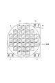
図4は、ウエハステージ4上に設置されている各基準マークの形状及び配置を示す平面図である。ウエハステージ4のコーナーには、基準プレート11がウエハ3表面とほぼ同じ高さで設置されている。基準プレート11には、ウエハアライメント検出系16が検出する基準マーク40とレチクルアライメント検出系13又は透過型のレチクルアライメント検出系14が検出する基準マーク39とを備えている。基準プレート11は、ウエハステージ4の複数のコーナーに配置されていても良い。また、基準プレート11は、複数の基準マーク39、複数の基準マーク40を設けていても良い。レチクルアライメント用の基準マーク39とウエハアライメント用の基準マーク40との位置関係(XY方向)は既知であるとする。また、ウエハアライメント検出用の基準マーク40とレチクルアライメント用の基準マーク39とは、共通のマークであっても良い。
FIG. 4 is a plan view showing the shape and arrangement of each reference mark installed on the wafer stage 4. At the corner of the wafer stage 4, the
フォーカス検出系15は、検出光をウエハ3表面に投射する投射系と、そのウエハ3からの反射光を受光する受光系とを備えており、フォーカス検出系15の検出結果は、制御部Cに出力される。制御部Cは、フォーカス検出系15の検出結果に基づいてZステージを駆動させ、Zステージに保持されているウエハ3のZ方向における位置(フォーカス位置)及び傾斜角を許容範囲に収めるように調整する。
The
ウエハアライメント検出系16は、検出光をウエハ3上のマーク19や基準プレート11上のウエハアライメント検出用の基準マーク40に投射する投射系と、該マークからの反射光を受光する受光系とを備えている。ウエハアライメント検出系16の検出結果は、制御部Cに出力される。制御部Cは、ウエハアライメント検出系16の検出結果に基づいてウエハステージ4をXY方向に駆動させることで、ウエハステージ4に保持されているウエハ3のXY方向における位置を調整することが可能である。露光装置Eは、ウエハアライメント検出系16のベストフォーカス位置を迅速に取得するためにウエハ3の表面位置を検出するAF検出系(フォーカス検出系)41を備える。AF検出系41は、フォーカス検出系15と同じく検出光をウエハ3表面に投射する投射系と、そのウエハ3からの反射光を受光する受光系とを備えている。フォーカス検出系15は、投影光学系6のベストフォーカス位置を取得するために用いられるのに対して、AF検出系41は、ウエハアライメント検出系16のベストフォーカス位置を取得するために用いられる。
The wafer
ウエハアライメント検出系16の形態としては、大きく2つの方式が存在する。1つ目の方式は、投影光学系6を介さず個別に構成されていて、ウエハ3上のマーク19、基準マーク40を光学的に検出するオフアクシスアライメント検出系(Off-axis AA、OA検出方式)である。2つ目の方式は、特にi線露光装置で使用される、投影光学系6を介して非露光光のアライメント波長を用いてマーク19、基準マーク40を検出するTTL−AA(Through The Lens アライメント)方式である。本実施形態ではOA検出方式のウエハアライメント検出系16を用いて説明するが、TTL−AA方式でも構わない。
There are two major types of wafer
図1は、検出装置Dのうちウエハアライメント検出系16とAF検出系41との構成を示す概略図である。ウエハアライメント検出系16の照明光源20は、赤外光(例えば、1000〜1500nm)及び可視光(例えば、400〜800nm)を発生する。照明光源20で発生された光は、第1リレー光学系21、波長フィルター板22、及び第2リレー光学系23を通り、ウエハアライメント検出系16の瞳面(物体面に対する光学的なフーリエ変換面)に配置された開口絞り24に到達する。図2は、照明光源20と開口絞り24とでの各ビーム径を比較する図である。図2に示すように、開口絞り24でのビーム径37は、照明光源20でのビーム径36よりも十分に小さい。
FIG. 1 is a schematic diagram showing the configuration of the wafer
波長フィルター板22は、透過波長帯の異なる複数のフィルターを含み、制御部Cからの命令でフィルターの切換を行う。開口絞り24は、照明σの異なる複数の絞りを含み、制御部Cからの命令で絞りの切換を行うことで、照明σを変更することができる。本実施形態では、波長フィルター板22と開口絞り24とがそれぞれ複数のフィルターと複数の絞りを備えているが、波長フィルター板22と開口絞り24とは別に、フィルターと絞りとを追加してもよい。本実施形態の波長フィルター板22は、可視光を透過するフィルターと赤外光を透過するフィルターとを備えており、これらのフィルターを切り替えることによりマークの検出に使用する光の波長を選択できる。赤外光に対して透過性を有するSiウエハの裏面に置かれたマークを計測する際には、赤外光を透過するフィルターが使用される。
The
開口絞り24まで到達した光は、第1照明光学系25、第2照明光学系27を通って偏光ビームスプリッター28に導かれる。偏光ビームスプリッター28により反射された紙面に垂直なS偏光は、NA絞り26、プリズム63、λ/4板29を透過して円偏光に変換され、対物レンズ30を通ってウエハ3に形成されたマーク19を照明する(照明光は図1中の実線で示す)。NA絞り26は、絞り量を変えることで、NAを変えることができる。NA絞り26の絞り量は、制御部Cからの命令で変更できる。プリズム63については、図5の説明で後述するが、アライメント光を透過する特性を持っている。
The light that reaches the
マーク19からの反射光(図1中の1点波線で示す)は、再度対物レンズ30及びλ/4板29を通って、今度は紙面に平行なP偏光に変換される。P偏光は、プリズム63、偏光ビームスプリッター28を透過し、リレーレンズ31、第1結像光学系32、コマ収差を調整する光学部材35、第2結像光学系33、波長シフト差を調整する光学部材38を通過する。光学部材38を通過したP偏光は、マーク19の検出信号を光電変換素子34(例えば、CCDカメラ)上に形成する。
Reflected light from the mark 19 (indicated by a one-dot dashed line in FIG. 1) passes through the
通常、ウエハアライメント検出系16により、マーク19を観察してマーク19の位置を検出する場合、マーク19上に塗布又は形成された透明層のため、単色光や狭い波長帯域の光では干渉縞が発生してしまう。そのため、アライメント信号に干渉縞の信号が加算された状態で検出され、マーク19を高精度に検出できなくなる。従って、一般的にウエハアライメント検出系16の照明光源20としては、マーク19を干渉縞の少ない信号として検出するために、広帯域の波長を持つものが使用される。
Usually, when the position of the
図5及び図6は、AF検出系41がフォーカス計測している状態を示す図である。図5は、AF検出系41がウエハ3にフォーカス計測光(AF光)を照射している様子を示している。光源55から照射されたAF光は、レンズ56を通してパターン板57を照明する。光源55は、可視光帯域(Siを透過しない400〜800nmの波長)の光を発生する。ウエハ3に照射されるAF光は、ウエハ3を透過しない。パターン板57は、ガラス基板にスリットパターンが描画されており、パターン板57の中心部に描画されたスリットパターンを照明されたAF光は、レンズ58を通りミラー59で反射されてレンズ60に到達する。パターン板57以降のAF光は、説明の都合上、主光線のみを書くが、実際にはNAを持った光線である。AF光は、レンズ60の中心ではなく、レンズ60の中心から偏心した部分に到達し、レンズ60で屈折することによって、基準ミラー61を通過し、レンズ62に到達する。レンズ62に到達した光も、レンズ62の中心ではなく、レンズ62の中心から偏心した部分に到達する。レンズ62で屈折したAF光は、プリズム63に到達する。プリズム63は、AF光を反射し、アライメントに使う光が透過する特性を有する。プリズム63で反射したAF光は、λ/4板29を透過し、レンズ30に到達する。AF光はレンズ30の中心ではなく、レンズ30の中心から偏心した部分に到達し、レンズ30で屈折することによって、図5に示すようにウエハ3に入射角度θで斜入射する。
5 and 6 are diagrams illustrating a state in which the
図6は、照射されたAF光がウエハ3で反射され、反射光がAF検出系41により受光される様子を示している。ウエハ3で反射されたAF光は、照明した時と同じ角度θでウエハ3から反射され、レンズ30に到達する。このとき、AF光は、レンズ30の中心ではなく、レンズ30の中心から偏心した部分に到達して、レンズ30で屈折することによって、λ/4板29を透過し、プリズム63に到達する。プリズム63で反射したAF光は、レンズ62に到達する。このとき、AF光はレンズ62の中心ではなく、レンズ62の中心から偏心した部分に到達し、レンズ62で屈折することによって、基準ミラー61を通過し、レンズ60に到達する。このとき、AF光はレンズ60の中心ではなく、レンズ60の中心から偏心した部分に到達し、レンズ60で屈折することによって、レンズ64の中心に到達し、レンズ64を透過し、AF検出センサー65で受光される。
FIG. 6 shows how the irradiated AF light is reflected by the
上記図5及び図6を用いた説明から、ウエハ3がフォーカス方向(Z方向)に移動すると、それに応じてAF検出センサー65におけるAF光を受光する位置がずれることが分かる。このように、AF検出系41は、ウエハ3の面位置を計測することが可能である。
From the description with reference to FIGS. 5 and 6, it can be seen that when the
図7は、AF検出系41内の基準計測を説明する図である。パターン板57の周辺部に照明されたAF光は、レンズ58の中心から偏心した部分に到達し、レンズ58で屈折しミラー59で反射される。ミラー59で反射したAF光は、レンズ60の中心から偏心した部分に到達し、レンズ60で屈折して基準ミラー61で反射され、今度はレンズ60の中心に到達する。レンズ60の中心を透過したAF光は、レンズ64の中心から偏心した部分に到達し、レンズ64で屈折してAF検出センサー65で受光される。AF検出系41内の基準計測では、AF光は、ウエハ3に到達することなく、AF光が直接AF検出センサー65で受光された位置が、AF検出系41によるフォーカス計測の基準となる。AF検出系41内の基準とウエハ3に対するフォーカス計測結果との差分から、ウエハ3のフォーカス位置を求めることが可能となる。
FIG. 7 is a diagram for explaining reference measurement in the
図5〜図7に示したAF検出系41によるフォーカス計測は、ウエハアライメント検出系16がマーク19を検出するためのベストフォーカス位置を計測するものではなく、ウエハ3の表面位置を検出するためのものである。すなわち、AF検出系41によるフォーカス計測は、ウエハアライメント検出系16におけるマーク19の像のファーカス状態を許容範囲に収めるようにするものである。従って、AF検出系41は、ウエハ3の表面で反射されたAF光を検出するため、ウエハ3の裏面に設けられたマークのフォーカス位置を直接検出することはできない。
The focus measurement by the
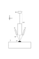
次に、図8及び図9を用いて、ウエハ3の表面にマーク19が配置されている場合に、ウエハアライメント検出系16がマーク19を検出するベストフォーカス位置を求める手法について説明する。イメージオートフォーカス計測では、図8に示すように、AF検出系41は、まずAF光42をウエハ3の表面のマーク19に投射し、反射光を受光する。なお、図8では、ウエハアライメント検出系16の外部にAF検出系41を配置した構成を図示しているが、ウエハアライメント検出系16の内部にAF検出系41を配置される構成でも良い。制御部Cは、受光した反射光の位置がAF検出系41のAF検出センサー65の中心に来るようにウエハステージ4を駆動することで、ウエハ3表面のマーク19のフォーカス位置を取得することができる。そして、制御部Cは、その取得したフォーカス位置を用いてウエハアライメント検出系16のフォーカス位置をマーク19に概ね合わせることができる。図9は、ウエハ3の表面にウエハアライメント検出系16のフォーカスが概ね合った状態で、マーク19にウエハアライメント検出系16からの計測光43が照射されている様子を示す図である。AF検出系41は、ウエハ3表面のマーク19にフォーカスが合っているが、ウエハアライメント検出系16が画像処理したマーク19のコントラストが最も高くなるフォーカス位置を求める必要がある。図9に示す状態からZ方向にウエハステージ4を駆動させ、ウエハアライメント検出系16が各フォーカス位置でアライメント計測を行うことで、マーク19のコントラストが最も高くなるフォーカス位置を見つけることができる(イメージオートフォーカス計測)。つまり、AF検出系41がウエハ3の表面を計測し、それによりウエハ3の表面にウエハアライメント検出系16のフォーカスが概ね合っている状態を基準として、ウエハアライメント検出系16は、+Z方向と−Z方向とでアライメント計測する。
Next, a method for obtaining the best focus position where the wafer
図10は、ウエハアライメント検出系16が図9に示す状態からイメージオートフォーカス計測を行って得られたコントラストカーブ47を示すグラフである。このフォーカス位置とコントラストとの関係から、ウエハアライメント検出系16の最もコントラストの高いベストフォーカス位置を求めることができる。例えば、最もコントラストの高いフォーカス位置は、図10に示すグラフから2次フィッティングや重心計算を実施することで求めることができる。また、図10では、簡単のためにイメージオートフォーカス計測による3つのフォーカス位置44、45、46を示しているが、計測点は、10点や20点などもっと増やしても良い。但し、計測点を増やしすぎると、計測に時間がかかり、スループット低下の原因となる。また、イメージオートフォーカス計測の手法の説明として、ウエハ3の表面にマーク19が設けられた図8を用いて説明したが、マーク19がウエハ3の表面の近傍にあれば、ウエハ3の表面にレジストが被覆されていてもかまわない。
FIG. 10 is a graph showing a
次に、図11及び図12を用いて、ウエハ3の裏面にマーク19が配置されている場合に、イメージオートフォーカス計測の手法を適用した場合について説明する。ウエハ3の裏面にマーク19がある場合も、AF検出系41は、まずAF光42をウエハ3の表面に投射し、反射光を受光する。このとき、制御部Cは、受光した反射光の位置がAF検出系41のAF検出センサー65の中心に来るようにウエハステージ4を駆動することで、ウエハ3の表面のフォーカス位置を取得することができる。そして、制御部Cは、その取得したフォーカス位置を用いてウエハアライメント検出系16のフォーカス位置をウエハ3の表面に概ね合わせることができる。図12は、ウエハ3の表面にウエハアライメント検出系16のフォーカスが概ね合った状態で、ウエハアライメント検出系16からの計測光43が照射されている様子を示す図である。図12に示す状態では、ウエハ3の裏面に設けられたマーク19に照射された赤外光(計測光)43は、ウエハアライメント検出系16の光電変換素子34に結像していない。
Next, a case where an image autofocus measurement method is applied when the
図13は、ウエハアライメント検出系16が図12に示す状態からイメージオートフォーカス計測を行って得られたコントラストカーブ48を示すグラフである。各フォーカス位置44、45、46でのコントラストは低く、ウエハ3の裏面側のマーク19を検出できていない。ウエハ3の裏面にマーク19が置かれている場合、ウエハ3の厚みが数100μm程度のこともあり、AF検出系41で検出したウエハ3の表面を基準とするイメージオートフォーカス計測では、ウエハ3の裏面側のマーク19を迅速に検出することはできない。ウエハ3の表面を基準とするイメージオートフォーカス計測の計測レンジを大幅に広げれば、ウエハ3の厚みが数100μmでも、ウエハ3の裏面側のマーク19をウエハアライメント検出系16により検出することは可能である。しかし、その場合、計測点数が大幅に増えてしまい、計測時間が増え、スループットが低下する。
FIG. 13 is a graph showing a
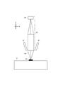
次に、図14を用いて、ウエハ3の裏面にマーク19が設けられた場合でも、ウエハアライメント検出系16のベストフォーカス位置を迅速に求める手法について説明する。この手法では、ウエハ3の厚みと屈折率とを利用して、イメージオートフォーカス計測の開始点を決定する。図3の入力器18に入力されたウエハ3の厚みと屈折率とを基に、計算器17は、ウエハ3の裏面側のマーク19にウエハアライメント検出系16のフォーカスが合うためのオフセット量を計算し、ウエハステージ4にオフセット量だけ駆動するように指示する。図14中の(1)は、裏面にマーク19が設けられたウエハ3の表面をAF検出系41が検出している様子を示す図である。AF検出系41は、図14中の(1)に示すようなウエハ3の表面を検出した状態のままでは、ウエハ3の表面にフォーカスが概ね合っているウエハアライメント検出系16ではマーク19を検出することはできない。図14中の(2)は、このときの、ウエハ3の裏面に設けられたマーク19に照射された計測光43がウエハアライメント検出系16の光電変換素子34に結像していない様子を示す図である。ウエハ3の厚み49は、数100μm程度の量であり、図14中の(2)では、ウエハアライメント検出系16は、この厚みに対応する量(オフセット量50)だけデフォーカスしている。
Next, a method for quickly obtaining the best focus position of the wafer
オフセット量50は、入力器18に入力されたウエハ3の厚み49と屈折率とを基に計算器17によって算出される。制御部Cは、ウエハ3の表面をAF検出系41が計測した図14中の(1)の状態から、計算器17により算出されたオフセット量50の分だけウエハステージ4をZ方向に駆動させる。そうすると、図14中の(3)に示すように、ウエハ3の裏面側のマーク19にウエハアライメント検出系16のフォーカスを合わせることができる。オフセット量50は、(ウエハ3の厚み49)/(ウエハ3の屈折率)で算出することができ、ウエハ3が例えば200μm厚のSi基板の場合、200μm/3.5(Siの屈折率)でおおよそ57μmとなる。このように、ウエハ3の厚み49と屈折率から算出されたオフセット量50を使えば、ウエハ3の裏面側のマーク19に対しても迅速にイメージオートフォーカス計測を行うことが可能となる。
The offset
図15(特に図15中の右側部分)は、ウエハアライメント検出系16が図14中の(3)の状態からイメージオートフォーカス計測を行って得られたコントラストカーブ54を示すグラフである。図15の各フォーカス位置51、52、53でのコントラストは高く、ウエハ3の裏面側のマーク19をウエハアライメント検出系16が検出できていることを示している。図12(及び図14中の(2))の状態、すなわちウエハ3の表面からイメージオートフォーカス計測したときのコントラストカーブを図13に示した。従って、図13に示すコントラストカーブは、フォーカス位置44〜46を含む図15中の左側部分のコントラストカーブに対応する。図15に示すコントラストカーブ54におけるフォーカス位置52と45との差分がオフセット量50を意味している。この図15に示すようなフォーカス位置とコントラストとの関係のデータから、ウエハ3の裏面側のマーク19に対しても、その位置をウエハアライメント検出系16が迅速にかつ高精度に求めることができる。
FIG. 15 (particularly the right portion in FIG. 15) is a graph showing a
上記の説明では、ウエハ3の厚みと屈折率とを入力器18に入力し、(ウエハ3の厚み49)/(ウエハ3の屈折率)を計算器17が計算してオフセット量50を算出するとしている。しかし、入力器18にオフセット量50を直接入力しても構わない。入力器18にオフセット量50を直接入力すると、(ウエハ3の厚み)/(ウエハ3の屈折率)の計算を手動で行う手間が生じるが、計算器17を削除できると言うコスト上のメリットがある。入力器18及び計算器17は、オフセット量50すなわちウエハアライメント検出系16におけるマーク19の像のフォーカス状態を示す情報を求める処理部Pを構成している。
In the above description, the thickness and the refractive index of the
本実施形態では、可視光を斜入射させるAF検出系41と、赤外光を用いるウエハアライメント検出系16とを用いて、ウエハ3の裏面に設けられたマーク19に対するイメージオートフォーカス計測を行った。これに対して、さらに、AF検出系41とウエハアライメント検出系16とを用いて、ウエハ3の上に塗布されたレジスト66の裏面に設けられたマーク19の位置を検出することができる。図16は、レジスト66の裏面にあるマーク19に対するイメージオートフォーカス計測の様子を示す図である。この場合、上述のAF検出系41では可視光がレジスト66を透過してしまい、レジスト66の表面の位置を検出できないため、レジスト66の表面の位置を検出するために検出系67を使用する。検出系67は、ウエハアライメント検出系16の中に構成されており、エアー(気体)68をレジスト66の表面に向けて噴射し、レジスト66から跳ね返るエアーの強度(圧力)によりレジスト66の表面高さを検出する。検出系67が検出したレジスト66の表面高さと、レジスト66の厚み49と、屈折率とに基づいて、レジスト66の裏面側のマーク19に対するイメージオートフォーカス計測が可能となる。
In the present embodiment, image autofocus measurement is performed on the
制御部Cは、レジスト66の表面位置を検出系67が計測した図16中の(1)の状態から、オフセット量50の分だけウエハステージ4を駆動させる。そうすると、図16中の(2)のようにレジスト66の裏面側のマーク19にウエハアライメント検出系16のフォーカスを概ね合わせることができる。オフセット量50は、(レジスト66の厚み49)/(レジスト66の屈折率)で算出することができる。例えば200μm厚のレジスト66の場合、オフセット量50は、200μm/1.5(レジスト66の屈折率)でおおよそ133μmとなる。図16中の(2)の状態からイメージオートフォーカス計測を開始することで、レジスト66の裏面にあるマーク19のベストフォーカス位置を迅速に求めることができる。このように、マーク19を裏面に有する被測定物の厚みと屈折率とから算出されたオフセット量50を使えば、ウエハ3以外の被測定物の裏面に設けられたマーク19に対してもイメージオートフォーカス計測を行うことが可能となる。
The controller C drives the wafer stage 4 by an offset
レジスト66の表面を計測するセンサーは、検出系67の代わりに、静電容量センサー等を適用しても良い。静電容量センサーは、レジスト66の表面に電圧を印加したときに発生する電荷量を検出することによって、静電容量センサーからレジスト66の表面までの高さを検出する。静電容量センサーからレジスト66の表面までの距離が近ければ、電圧を加えたときに発生する電荷量は大きくなり、静電容量センサーからレジスト66の表面までの距離が遠ければ、電圧を加えたときに発生する電荷量は小さくなる。このように静電容量センサーは、一定の電圧を静電容量センサーとレジスト66の表面にかけた際に発生する電荷量を検出することで、静電容量センサーからレジスト66の表面までの距離を算出する。
As a sensor for measuring the surface of the resist 66, a capacitance sensor or the like may be applied instead of the
露光装置Eが1ロット25枚のウエハ3を露光する場合、1枚目のウエハ3のマーク(第1マーク)19に対してのみイメージオートフォーカス計測を実施する。そして、2枚目以降のウエハ3のマーク(第2マーク)19に対してはAF検出系41による計測結果のみでウエハ3の裏面側のマーク19に対するフォーカスを合わせることが可能である。ロット内の1枚目のウエハ3に対しては、図14中の(3)に示すように、制御部Cは、AF検出系41の計測値からオフセット量50だけウエハステージ4を駆動させてから裏面側のマーク19に対してイメージオートフォーカス計測を行う。このとき、イメージオートフォーカス計測で算出された裏面側のマーク19に対するウエハアライメント検出系16のベストフォーカス位置と、AF検出系41がウエハ3の表面を計測したフォーカス位置との差分69を求める。制御部Cは、2枚目以降のウエハ3に対しては、ウエハ3の表面位置をAF検出系41が計測した状態から、1枚目のウエハ3のイメージオートフォーカス計測から求めた差分69だけウエハステージ4を駆動させる。そして、その状態で裏面側のマーク19をウエハアライメント検出系16により計測する。こうすることで、1枚目のウエハ3に対してのみイメージオートフォーカス計測するだけで、他の24枚のウエハ3に対しても高精度にアライメント計測することが可能になる。
When the exposure apparatus E exposes 25 lots of
次に、ウエハアライメント検出系16とAF検出系41とを用いたSiウエハ3の厚みの計測について説明する。図17は、ウエハアライメント検出系16とAF検出系41とを用いて、ウエハ3の厚みを計測している様子を示す図である。AF検出系41は、ウエハ3の表面の第2フォーカス位置を計測(検出)しており、一方、ウエハアライメント検出系16は、ウエハ3の裏面にあるマーク19の第1フォーカス位置を計測(検出)している。計算器17は、AF検出系41が計測するウエハ3の表面のフォーカス位置と、ウエハアライメント検出系16が検出するウエハ3の裏面のフォーカス位置との差分に基づいてウエハ3の厚みを算出することができる。これに対して、計算器17は、上記差分にウエハ3の材質であるSiの屈折率をかけることで、ウエハ3の幾何学的厚みとしての厚みを算出することができる。なお、Siの屈折率は、入力器18に予め入力されている値を使用することが望ましいが、本実施形態のように検出装置Dを露光装置E内に設置している場合には、露光装置E内の制御部Cに予め入力されている値を使用しても良い。
Next, measurement of the thickness of the
また、上記のような厚み計測を応用することで、貼り合わせウエハの一部であるSi板の厚みのみを計測することができる。以下、説明の簡単化のために、Si板には上記Siウエハと同一の符号を付す。図18は、貼り合わせウエハのSi板3の厚みのみを計測している様子を示す図である。ここで、一例としての貼り合わせウエハは、基材75とSi板3とが接着剤76を介して貼り合わされたものである。また、この場合のSi板3は、表面側と裏面側とが平行ではなく、たわみを持ったまま薄化されている。制御部Cは、このようなSi板3の厚みも、上記と同様に算出することができる。特に、図18に示すように、複数のアライメントマーク19a〜19cがそれぞれ異なる像高として配置されている場合でも、上記のような厚み計測をそれぞれ実施することで、制御部Cは、ウエハ全面の厚みのバラツキを特定することができる。
In addition, by applying the thickness measurement as described above, only the thickness of the Si plate that is a part of the bonded wafer can be measured. Hereinafter, for simplification of description, the same reference numerals as those of the Si wafer are attached to the Si plate. FIG. 18 is a diagram illustrating a state in which only the thickness of the
図19は、図18に示した3つのアライメントマーク19a〜19cの設置部分におけるSi板3の厚みをそれぞれ計測した結果を示すグラフである。この図19において、横軸は、中心像高(アライメントマーク19bの配置位置)を基準としたX方向の距離である。一方、縦軸は、AF検出系41が検出したSi板3の表面を0μmとし、ウエハアライメント検出系16が検出したアライメントマーク19a〜19cのフォーカス位置にSiの屈折率をかけて得られたSi板3の厚みであり、マイナス方向で表示している。図19によれば、Si板3の厚みは、設定値として200μmに薄化され、中心像高では210μmとなるが、周辺像高では240μmおよび250μmとなる。すなわち、Si板3の厚みには、中心部と周辺部とで差があり、かつ周辺部のみで比較しても左右差があることがわかる。なお、制御部Cは、計測点数をウエハ全面に広げて計測させることで、ウエハの3次元情報を算出することができる。このように、本実施形態に係るウエハアライメント検出系16とAF検出系41とによれば、露光装置E内で簡易的にSiウエハや貼り合わせウエハのSi板の厚みを計測することができる。
FIG. 19 is a graph showing the results of measuring the thickness of the
さらに、ウエハアライメント検出系16とAF検出系41とを用いたフォーカス補正について説明する。この場合、例えば図3に示すステージ基準プレート11をAF検出系41とウエハアライメント検出系16とが計測することでフォーカス補正を行う。具体的には、まずAF検出系41がステージ基準プレート11をフォーカス計測する。次に、ウエハアライメント検出系16がステージ基準プレート11上のマークをイメージオートフォーカス計測する。そして、制御部Cがそれぞれで得られたフォーカス計測値を合わせることで補正を行う。これにより、ステージ基準プレート11上のマークに対して、AF検出系41のフォーカス計測値と、ウエハアライメント検出系16のイメージオートフォーカス計測で得られるフォーカス計測値とは、同一の値となる。なお、ここではステージ基準プレート11上のマークを基準としたが、AF検出系41とウエハアライメント検出系16とのフォーカス計測値を取得できるならば、例えばウエハ3上のマークを基準としても良い。
Further, focus correction using the wafer
このように、ウエハアライメント検出系16とAF検出系41とから構成される検出装置は、まず、ウエハ3、またはウエハ3以外の被測定物の裏面に設けられたマーク19に対してもイメージオートフォーカス計測を好適に実施することができる。また、この検出装置は、露光装置E内にて、ウエハ3、またはウエハ3以外の被測定物の厚み(SiウエハまたはSi板の厚み)を検出することができる。これにより、制御部Cは、計算器17から取得した厚みを自動で定期的にモニターすることで、厚みに変動が生じたと判定した場合には、露光処理後にウエハ3に薄化処理を実施する薄化装置へフィードバックすることができる。また、検出された厚みを、薄化装置に限らず、例えば露光処理後にウエハ3にエッチング処理を実施するエッチング装置にフィードバックすることで、最適なエッチング時間で所望の貫通VIAを形成することができ、デバイスの歩留まり向上を実現し得る。さらに、この検出装置は、ウエハ面内の局所的な厚みのバラツキも特定できるため、エッチング装置に対して、ウエハ面内でエッチング時間に差を付けさせることも可能となり、さらに歩留まりの向上を期待できる。
As described above, the detection apparatus constituted by the wafer
以上のように、本実施形態によれば、Siウエハなどの被測定物の裏面に設けられたマークの位置に加え、被測定物の厚みを迅速かつ高精度に検出するのに有利な検出装置を提供することができる。 As described above, according to the present embodiment, in addition to the position of the mark provided on the back surface of the object to be measured such as a Si wafer, the detection device is advantageous for detecting the thickness of the object to be measured quickly and with high accuracy. Can be provided.
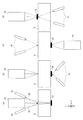
なお、上記の説明では、AF検出系41としてウエハアライメント検出系16の外(外周領域)に配置されているAF検出系41を用いたが、本発明は、このようなAF検出系のみに限定するものではない。図20は、ウエハアライメント検出系16とAF検出系41との他の配置例を示す図である。図20(a)は、比較のために、ウエハアライメント検出系16とAF検出系41とをともにウエハ3の表面側に配置した第1実施形態の配置を示す図である。これに対して、ウエハ3の裏面側にウエハアライメント検出系16またはAF検出系41を配置することが可能な場合には、以下に示すように、ウエハアライメント検出系16とAF検出系41とをウエハ3の表面側と裏面側とに分離して配置することもできる。まず、図20(b)は、ウエハ3の裏面側のマーク19を検出するために、赤外光を光源とするウエハアライメント検出系16をウエハ3の表面側に配置し、可視光を光源とするAF検出系41をウエハ3の裏面側に配置した例を示す図である。次に、図20(c)は、ウエハ3の裏面側のマーク19を検出するために、可視光を光源とするウエハアライメント検出系16をウエハ3の裏面側に配置し、赤外光を光源とするAF検出系41をウエハ3の表面側に配置した例を示す図である。そして、図20(d)は、ウエハ3の表面側のアライメントマーク19を検出するために、可視光を光源とするウエハアライメント検出系16をウエハ3の表面側に配置し、赤外光を光源とするAF検出系41をウエハ3の裏面側に配置した例を示す図である。さらに、この場合も、AF検出系41に換えて、図16に示した検出系67を用いてウエハ3の厚みを計測しても良い。
In the above description, the
(第2実施形態)
上記第1実施形態では、ウエハ3の表面位置を検出するフォーカス検出系41、67を用いて、ウエハ3の裏面に設けられたマーク19に対するウエハアライメント検出系16のフォーカス位置を迅速に取得した。これに対して、本実施形態では、ウエハアライメント検出系16として、第1検出モードと第2検出モードとの2つの検出モードに切り替え可能なものを使用する。さらに、本実施形態では、第1実施形態で用いたウエハ3の表面位置を検出するフォーカス検出系41、67を用いない。ウエハアライメント検出系16は、第1検出モードで、マーク19との間隔を第1ピッチで変更しながら第1検出精度でマーク19を検出し、一方、第2検出モードで、マーク19との間隔を第2ピッチで変更しながら第2検出精度でマーク19を検出する。そのとき、第2ピッチは、第1ピッチより小さく、第2検出精度は、第1検出精度より高い精度とする。すなわち、第1検出モードは、検出精度は低いが、一度に広い領域を検出できるワイドピッチの検出モードである。一方、第2検出モードは、検出領域は狭いが、検出精度が高いファインピッチの検出モードである。
(Second Embodiment)
In the first embodiment, the focus position of the wafer
図21は、ウエハ3の表面側に配置されたウエハアライメント検出系16をワイドピッチの第1検出モードでウエハ3の裏面側のマーク19を計測したときのコントラストカーブを示すグラフである。ウエハアライメント検出系16の従来のイメージオートフォーカス計測のピッチよりもワイドピッチの第1検出モードでイメージオートフォーカス計測をすることで、マーク19を計測するための概略のフォーカス位置72を迅速に取得することができる。次いで、ウエハアライメント検出系16の検出モードを検出精度が高い第2検出モードに切り替えてフォーカス位置72からイメージオートフォーカス計測を開始する。このように、ウエハアライメント検出系16の検出モードを切り替えて2段階でのイメージオートフォーカス計測をすることで、マーク19を計測するためのベストフォーカス位置を迅速に取得することができる。図22は、第1検出モードで得られたフォーカス位置72から第2検出モードでイメージオートフォーカス計測を行った場合のコントラストカーブを示すグラフであり、ベストフォーカス位置74を取得していることが分かる。
FIG. 21 is a graph showing a contrast curve when the wafer
(デバイスの製造方法)
次に、本発明の一実施形態のデバイス(半導体デバイス、液晶表示デバイスなど)の製造方法について説明する。半導体デバイスは、ウエハに集積回路を作る前工程と、前工程で作られたウエハ上の集積回路チップを製品として完成させる後工程を経ることにより製造される。前工程は、前述の露光装置を使用して感光剤が塗布されたウエハを露光する工程と、ウエハを現像する工程を含む。後工程は、アッセンブリ工程(ダイシング、ボンディング)と、パッケージング工程(封入)を含む。液晶表示デバイスは、透明電極を形成する工程を経ることにより製造される。透明電極を形成する工程は、透明導電膜が蒸着されたガラス基板に感光剤を塗布する工程と、前述の露光装置を使用して感光剤が塗布されたガラス基板を露光する工程と、ガラス基板を現像する工程を含む。本実施形態のデバイス製造方法によれば、従来よりも高品位のデバイスを製造することができる。
(Device manufacturing method)
Next, a method for manufacturing a device (semiconductor device, liquid crystal display device, etc.) according to an embodiment of the present invention will be described. A semiconductor device is manufactured through a pre-process for producing an integrated circuit on a wafer and a post-process for completing an integrated circuit chip on the wafer produced in the pre-process as a product. The pre-process includes a step of exposing a wafer coated with a photosensitive agent using the above-described exposure apparatus, and a step of developing the wafer. The post-process includes an assembly process (dicing and bonding) and a packaging process (encapsulation). A liquid crystal display device is manufactured through a process of forming a transparent electrode. The step of forming the transparent electrode includes a step of applying a photosensitive agent to a glass substrate on which a transparent conductive film is deposited, a step of exposing the glass substrate on which the photosensitive agent is applied using the above-described exposure apparatus, and a glass substrate. The process of developing is included. According to the device manufacturing method of the present embodiment, it is possible to manufacture a higher quality device than before.
以上、本発明の好ましい実施形態について説明したが、本発明は、これらの実施形態に限定されず、その要旨の範囲内で種々の変形および変更が可能である。 As mentioned above, although preferable embodiment of this invention was described, this invention is not limited to these embodiment, A various deformation | transformation and change are possible within the range of the summary.
3 被測定物
16 ウエハアライメント検出系
41 AF検出系
D 検出装置
P 処理部
3 Measured
Claims (13)
前記被測定物を透過する光で前記被測定物の表面側から前記マークを照明し、該照明されたマークの像を検出する第1検出系と、
前記被測定物の表面の位置を検出する第2検出系と、
処理部と、を備え、
前記第1検出系は、前記マークの像を複数回検出し、前記処理部は、前記第1検出系による複数回の像検出結果に基づいて第1位置を求め、かつ、求めた第1位置と、前記被測定物の表面に対して前記第1検出系のフォーカスを合わせたときに前記第2検出系により検出された前記表面の位置を参照して得られた第2位置とに基づいて前記被測定物の厚みを求めることを特徴とする検出装置。 A detection device for detecting a mark provided on the back surface of the object to be measured,
A first detection system for illuminating the mark from the surface side of the object to be measured with light transmitted through the object to be measured, and detecting an image of the illuminated mark;
A second detection system for detecting the position of the surface of the object to be measured;
A processing unit,
The first detection system detects an image of the mark a plurality of times, and the processing unit obtains a first position based on a plurality of image detection results by the first detection system , and the obtained first position And a second position obtained by referring to the position of the surface detected by the second detection system when the first detection system is focused on the surface of the object to be measured. A detection apparatus characterized by obtaining a thickness of the object to be measured .
前記複数の厚みに基づいて前記被測定物の3次元情報を求める、ことを特徴とする請求項1ないし6のいずれか1項に記載の検出装置。 The processing unit obtains the thickness at the plurality of positions based on the first position and the second position acquired at the plurality of positions of the object to be measured,
It said plurality of based on the thickness determine the three-dimensional information of the object to be measured, that the detection apparatus according to any one of claims 1 to 6, characterized in.
前記基板を保持する保持部と、
前記保持部を移動させる駆動機構と、を有し、
被測定物としての前記基板の厚みを検出する、請求項1ないし8のいずれか1項に記載の検出装置を有することを特徴とする露光装置。 An exposure apparatus for exposing a substrate,
A holding unit for holding the substrate;
A drive mechanism for moving the holding portion,
Detecting the thickness of the substrate as an object to be measured, an exposure apparatus characterized by having a detecting apparatus according to any one of claims 1 to 8.
前記被測定物の表面の位置を検出する第2検出系と、を用いた、被測定物の厚みの検出方法であって、
前記第1検出系からの光の光軸方向における前記第1検出系に対する前記被測定物の位置を、前記被測定物の予め設定されている厚みと前記被測定物の屈折率とにより決定されたオフセット量に基づいて調整する工程と、
前記光軸方向における前記第1検出系に対する前記被測定物の位置を複数回変えた場合のそれぞれで前記第1検出系を用いて前記マークの像を検出する工程と、
前記第1検出系による複数回の像検出結果に基づいて第1位置を求め、さらに、求めた第1位置と前記第2検出系により検出された前記表面の位置を参照して得られた第2位置とに基づいて前記被測定物の厚みを取得する工程と、を有することを特徴とする検出方法。 A first detection system for illuminating a mark provided on the back surface of the object to be measured from the front side of the object to be measured with light passing through the object to be measured, and detecting an image of the illuminated mark;
A second detection system for detecting the position of the surface of the object to be measured, and a method for detecting the thickness of the object to be measured,
The position of the object to be measured with respect to the first detection system in the optical axis direction of light from the first detection system is determined by a preset thickness of the object to be measured and a refractive index of the object to be measured. Adjusting based on the offset amount,
Detecting an image of the mark using the first detection system in each case where the position of the object to be measured is changed a plurality of times with respect to the first detection system in the optical axis direction;
A first position is obtained based on a plurality of image detection results by the first detection system, and a first position obtained by referring to the obtained first position and the position of the surface detected by the second detection system. Obtaining the thickness of the object to be measured based on two positions .
前記工程で露光した基板を現像する工程と、
を含むことを特徴とするデバイス製造方法。 A step of exposing the substrate using the exposure apparatus according to claim 9 or 10 ;
Developing the substrate exposed in the step;
A device manufacturing method comprising:
Priority Applications (5)
| Application Number | Priority Date | Filing Date | Title |
|---|---|---|---|
| JP2012231653A JP6150490B2 (en) | 2012-10-19 | 2012-10-19 | Detection apparatus, exposure apparatus, and device manufacturing method using the same |
| TW102136354A TWI534558B (en) | 2012-10-19 | 2013-10-08 | Detection device, exposure apparatus, and device manufacturing method using same |
| US14/055,323 US9400436B2 (en) | 2012-10-19 | 2013-10-16 | Detection device, exposure apparatus, and device manufacturing method using same |
| EP13004976.0A EP2722714A3 (en) | 2012-10-19 | 2013-10-17 | Detection device, exposure apparatus and device manufacturing method using such an exposure apparatus |
| KR1020130124407A KR101672576B1 (en) | 2012-10-19 | 2013-10-18 | Detection device, exposure apparatus, and device manufacturing method using same |
Applications Claiming Priority (1)
| Application Number | Priority Date | Filing Date | Title |
|---|---|---|---|
| JP2012231653A JP6150490B2 (en) | 2012-10-19 | 2012-10-19 | Detection apparatus, exposure apparatus, and device manufacturing method using the same |
Publications (3)
| Publication Number | Publication Date |
|---|---|
| JP2014085123A JP2014085123A (en) | 2014-05-12 |
| JP2014085123A5 JP2014085123A5 (en) | 2015-12-03 |
| JP6150490B2 true JP6150490B2 (en) | 2017-06-21 |
Family
ID=49385090
Family Applications (1)
| Application Number | Title | Priority Date | Filing Date |
|---|---|---|---|
| JP2012231653A Active JP6150490B2 (en) | 2012-10-19 | 2012-10-19 | Detection apparatus, exposure apparatus, and device manufacturing method using the same |
Country Status (5)
| Country | Link |
|---|---|
| US (1) | US9400436B2 (en) |
| EP (1) | EP2722714A3 (en) |
| JP (1) | JP6150490B2 (en) |
| KR (1) | KR101672576B1 (en) |
| TW (1) | TWI534558B (en) |
Families Citing this family (10)
| Publication number | Priority date | Publication date | Assignee | Title |
|---|---|---|---|---|
| TWI571710B (en) * | 2014-12-30 | 2017-02-21 | 力晶科技股份有限公司 | Method and system for monitoring module actuation of alignment light source device in exposure apparatus |
| JP6207671B1 (en) * | 2016-06-01 | 2017-10-04 | キヤノン株式会社 | Pattern forming apparatus, substrate arranging method, and article manufacturing method |
| CN106247958A (en) * | 2016-07-11 | 2016-12-21 | 京东方科技集团股份有限公司 | Measurement equipment and measuring method |
| NL2019155A (en) | 2016-08-30 | 2018-03-06 | Asml Netherlands Bv | Position sensor, lithographic apparatus and method for manufacturing devices |
| JP2019096757A (en) * | 2017-11-24 | 2019-06-20 | 東京エレクトロン株式会社 | Method for obtaining deviation amount of measurement equipment, and method for calibrating transfer position data in processing system |
| EP3667423B1 (en) * | 2018-11-30 | 2024-04-03 | Canon Kabushiki Kaisha | Lithography apparatus, determination method, and method of manufacturing an article |
| JP7129325B2 (en) * | 2018-12-14 | 2022-09-01 | 東京エレクトロン株式会社 | Conveying method and conveying system |
| JP7173891B2 (en) * | 2019-02-14 | 2022-11-16 | キヤノン株式会社 | Measuring device, exposure device, and article manufacturing method |
| JP7446131B2 (en) | 2020-03-12 | 2024-03-08 | キヤノン株式会社 | Detection device, exposure device, and article manufacturing method |
| WO2022040228A1 (en) * | 2020-08-17 | 2022-02-24 | Tokyo Electron Limited | Method of pattern alignment for field stitching |
Family Cites Families (17)
| Publication number | Priority date | Publication date | Assignee | Title |
|---|---|---|---|---|
| EP0585041B1 (en) * | 1992-08-19 | 2000-11-02 | Canon Kabushiki Kaisha | Registration method usable with a projection optical system, exposure apparatus therefor and method of manufacturing a semiconductor device by using such exposure apparatus |
| US5474647A (en) * | 1993-11-15 | 1995-12-12 | Hughes Aircraft Company | Wafer flow architecture for production wafer processing |
| US5671054A (en) * | 1995-07-18 | 1997-09-23 | Nikon Corporation | Method and apparatus for measuring position of pattern formed on a substrate having a thickness |
| DE19733890C2 (en) * | 1996-08-04 | 2000-03-16 | Matsushita Electric Ind Co Ltd | Method for measuring a medium and device therefor |
| US5744814A (en) * | 1997-03-24 | 1998-04-28 | Nec Corporation | Method and apparatus for scanning exposure having thickness measurements of a film surface |
| US6376329B1 (en) * | 1997-08-04 | 2002-04-23 | Nikon Corporation | Semiconductor wafer alignment using backside illumination |
| US5781303A (en) * | 1997-08-29 | 1998-07-14 | Becton Dickinson And Company | Method for determining the thickness of an optical sample |
| AU2001225543A1 (en) * | 2000-01-21 | 2001-08-20 | Hamamatsu Photonics K.K. | Thickness measuring apparatus, thickness measuring method, and wet etching apparatus and wet etching method utilizing them |
| US6768539B2 (en) * | 2001-01-15 | 2004-07-27 | Asml Netherlands B.V. | Lithographic apparatus |
| KR100438787B1 (en) * | 2002-05-13 | 2004-07-05 | 삼성전자주식회사 | Method for measuring thickness of thin layer |
| JP2005005444A (en) * | 2003-06-11 | 2005-01-06 | Nikon Corp | Alignment device, aligner, alignment method and exposure method and positional-information detecting method |
| JP5018004B2 (en) * | 2006-10-11 | 2012-09-05 | 株式会社ニコン | Microscope, mark detection method, wafer bonding apparatus, and manufacturing method of stacked three-dimensional semiconductor device |
| US20080292177A1 (en) * | 2007-05-23 | 2008-11-27 | Sheets Ronald E | System and Method for Providing Backside Alignment in a Lithographic Projection System |
| TW200938803A (en) | 2008-03-07 | 2009-09-16 | Univ Nat Formosa | Device and method for testing thickness and gaps of transparent objects by means of dual optical probes |
| JP5406624B2 (en) | 2009-08-10 | 2014-02-05 | キヤノン株式会社 | Detection apparatus, exposure apparatus, and device manufacturing method |
| JP2012195380A (en) * | 2011-03-15 | 2012-10-11 | Nikon Corp | Mark detection method and device, and exposure method and device |
| JP6025346B2 (en) * | 2012-03-05 | 2016-11-16 | キヤノン株式会社 | Detection apparatus, exposure apparatus, and device manufacturing method |
-
2012
- 2012-10-19 JP JP2012231653A patent/JP6150490B2/en active Active
-
2013
- 2013-10-08 TW TW102136354A patent/TWI534558B/en active
- 2013-10-16 US US14/055,323 patent/US9400436B2/en active Active
- 2013-10-17 EP EP13004976.0A patent/EP2722714A3/en not_active Withdrawn
- 2013-10-18 KR KR1020130124407A patent/KR101672576B1/en active IP Right Grant
Also Published As
| Publication number | Publication date |
|---|---|
| TW201416805A (en) | 2014-05-01 |
| KR101672576B1 (en) | 2016-11-03 |
| EP2722714A2 (en) | 2014-04-23 |
| JP2014085123A (en) | 2014-05-12 |
| US9400436B2 (en) | 2016-07-26 |
| KR20140050562A (en) | 2014-04-29 |
| TWI534558B (en) | 2016-05-21 |
| US20140111788A1 (en) | 2014-04-24 |
| EP2722714A3 (en) | 2015-06-17 |
Similar Documents
| Publication | Publication Date | Title |
|---|---|---|
| JP6150490B2 (en) | Detection apparatus, exposure apparatus, and device manufacturing method using the same | |
| JP6025346B2 (en) | Detection apparatus, exposure apparatus, and device manufacturing method | |
| JP5385652B2 (en) | Position detection apparatus, exposure apparatus, position detection method, exposure method, and device manufacturing method | |
| JP5743958B2 (en) | Measuring method, exposure method and apparatus | |
| JP4944690B2 (en) | Method for adjusting position detection apparatus, position detection apparatus, exposure apparatus, and device manufacturing method | |
| US8810772B2 (en) | Position detector, position detection method, exposure apparatus, and method of manufacturing device to align wafer by adjusting optical member | |
| US20210255555A1 (en) | Control method of movable body, exposure method, device manufacturing method, movable body apparatus, and exposure apparatus | |
| TW201107905A (en) | Measurement apparatus, exposure apparatus, and device fabrication method | |
| US9939741B2 (en) | Lithography apparatus, and method of manufacturing article | |
| US10747116B2 (en) | Pattern forming apparatus and article manufacturing method | |
| JP2003142377A (en) | Projection aligner and method of measuring aberration | |
| KR101599577B1 (en) | Exposure apparatus, method of controlling the same and method of manufacturing device | |
| TWI358529B (en) | Shape measuring apparatus, shape measuring method, | |
| JP6226525B2 (en) | Exposure apparatus, exposure method, and device manufacturing method using them | |
| JP7418112B2 (en) | Pattern forming device and article manufacturing method | |
| JP6302185B2 (en) | Detection apparatus, exposure apparatus, and article manufacturing method | |
| JP6061912B2 (en) | Measuring method, exposure method and apparatus |
Legal Events
| Date | Code | Title | Description |
|---|---|---|---|
| A521 | Request for written amendment filed |
Free format text: JAPANESE INTERMEDIATE CODE: A523 Effective date: 20151019 |
|
| A621 | Written request for application examination |
Free format text: JAPANESE INTERMEDIATE CODE: A621 Effective date: 20151019 |
|
| A977 | Report on retrieval |
Free format text: JAPANESE INTERMEDIATE CODE: A971007 Effective date: 20160831 |
|
| A131 | Notification of reasons for refusal |
Free format text: JAPANESE INTERMEDIATE CODE: A131 Effective date: 20160906 |
|
| A521 | Request for written amendment filed |
Free format text: JAPANESE INTERMEDIATE CODE: A523 Effective date: 20161107 |
|
| TRDD | Decision of grant or rejection written | ||
| A01 | Written decision to grant a patent or to grant a registration (utility model) |
Free format text: JAPANESE INTERMEDIATE CODE: A01 Effective date: 20170425 |
|
| A61 | First payment of annual fees (during grant procedure) |
Free format text: JAPANESE INTERMEDIATE CODE: A61 Effective date: 20170523 |
|
| R151 | Written notification of patent or utility model registration |
Ref document number: 6150490 Country of ref document: JP Free format text: JAPANESE INTERMEDIATE CODE: R151 |