JP6140008B2 - Radiation imaging apparatus and radiation inspection apparatus - Google Patents
Radiation imaging apparatus and radiation inspection apparatus Download PDFInfo
- Publication number
- JP6140008B2 JP6140008B2 JP2013138444A JP2013138444A JP6140008B2 JP 6140008 B2 JP6140008 B2 JP 6140008B2 JP 2013138444 A JP2013138444 A JP 2013138444A JP 2013138444 A JP2013138444 A JP 2013138444A JP 6140008 B2 JP6140008 B2 JP 6140008B2
- Authority
- JP
- Japan
- Prior art keywords
- signal
- sensor
- unit
- row
- imaging apparatus
- Prior art date
- Legal status (The legal status is an assumption and is not a legal conclusion. Google has not performed a legal analysis and makes no representation as to the accuracy of the status listed.)
- Active
Links
Images


Classifications
-
- H—ELECTRICITY
- H04—ELECTRIC COMMUNICATION TECHNIQUE
- H04N—PICTORIAL COMMUNICATION, e.g. TELEVISION
- H04N5/00—Details of television systems
- H04N5/30—Transforming light or analogous information into electric information
- H04N5/32—Transforming X-rays
-
- H—ELECTRICITY
- H04—ELECTRIC COMMUNICATION TECHNIQUE
- H04N—PICTORIAL COMMUNICATION, e.g. TELEVISION
- H04N25/00—Circuitry of solid-state image sensors [SSIS]; Control thereof
- H04N25/50—Control of the SSIS exposure
- H04N25/57—Control of the dynamic range
- H04N25/59—Control of the dynamic range by controlling the amount of charge storable in the pixel, e.g. modification of the charge conversion ratio of the floating node capacitance
-
- H—ELECTRICITY
- H04—ELECTRIC COMMUNICATION TECHNIQUE
- H04N—PICTORIAL COMMUNICATION, e.g. TELEVISION
- H04N25/00—Circuitry of solid-state image sensors [SSIS]; Control thereof
- H04N25/60—Noise processing, e.g. detecting, correcting, reducing or removing noise
- H04N25/67—Noise processing, e.g. detecting, correcting, reducing or removing noise applied to fixed-pattern noise, e.g. non-uniformity of response
-
- H—ELECTRICITY
- H04—ELECTRIC COMMUNICATION TECHNIQUE
- H04N—PICTORIAL COMMUNICATION, e.g. TELEVISION
- H04N25/00—Circuitry of solid-state image sensors [SSIS]; Control thereof
- H04N25/60—Noise processing, e.g. detecting, correcting, reducing or removing noise
- H04N25/68—Noise processing, e.g. detecting, correcting, reducing or removing noise applied to defects
-
- H—ELECTRICITY
- H04—ELECTRIC COMMUNICATION TECHNIQUE
- H04N—PICTORIAL COMMUNICATION, e.g. TELEVISION
- H04N25/00—Circuitry of solid-state image sensors [SSIS]; Control thereof
- H04N25/60—Noise processing, e.g. detecting, correcting, reducing or removing noise
- H04N25/65—Noise processing, e.g. detecting, correcting, reducing or removing noise applied to reset noise, e.g. KTC noise related to CMOS structures by techniques other than CDS
Landscapes
- Engineering & Computer Science (AREA)
- Multimedia (AREA)
- Signal Processing (AREA)
- Transforming Light Signals Into Electric Signals (AREA)
- Measurement Of Radiation (AREA)
- Physics & Mathematics (AREA)
- Health & Medical Sciences (AREA)
- Life Sciences & Earth Sciences (AREA)
- General Physics & Mathematics (AREA)
- High Energy & Nuclear Physics (AREA)
- Molecular Biology (AREA)
- Spectroscopy & Molecular Physics (AREA)
Description
本発明は、放射線撮像装置及び放射線検査装置に関する。 The present invention relates to a radiation imaging apparatus and a radiation inspection apparatus.
特許文献1には、センサアレイの各センサが、照射された放射線量に応じた信号を保持する保持部(サンプルホールド回路)を有する放射線撮像装置が開示されている。特許文献1によると、放射線量に応じた信号は、各センサにおいて保持部によって個別に保持されるため、1フレームの読出(信号読出)と、次のフレームのための放射線の照射とを同時に行うことができる。
ところで、放射線撮像装置は、各センサにおいて、例えば2つの感度で信号をそれぞれ取得し、これらの信号を用いて画像データを生成する動作モード(例えば、ダイナミックレンジ拡張を行う動作モード等)を有しうる。この動作モードを達成する1つの方法として、2つの保持部を各センサに設け、各感度で得られた信号を、各保持部でそれぞれ保持して個別に読み出す方式が考えられる。 By the way, the radiation imaging apparatus has an operation mode (for example, an operation mode for performing dynamic range expansion or the like) in which each sensor acquires signals with two sensitivities and generates image data using these signals, for example. sell. As one method for achieving this operation mode, there can be considered a method in which two holding units are provided in each sensor, and signals obtained with respective sensitivities are individually held by each holding unit and read out individually.
各センサには、センサアレイの各行に対応して配された制御線を介して、制御信号が入力される。信号読出は、制御信号に応答して各センサから出力された信号を、信号読出部が行ごとに読み出すことによって為される。信号読出を行う際には、この制御信号により、制御線と交差する信号読出用の列信号線において電位変動が生じうる。そのため、信号を読み出すべき各センサを切り替えたときは当該電位変動が収まった後(所定期間が経過した後)に信号読出を行う必要があり、センサアレイの各センサから信号を読み出すのには相当の時間を要する。このことは、特にセンサパネルの大型化に伴って、センサアレイの行数が多くなり、また、信号線の配線容量が大きくなるため顕著になる。 A control signal is input to each sensor via a control line arranged corresponding to each row of the sensor array. The signal reading is performed by the signal reading unit reading the signal output from each sensor in response to the control signal for each row. When signal reading is performed, potential fluctuations may occur in the signal reading column signal line intersecting with the control line due to the control signal. For this reason, when each sensor from which a signal is to be read is switched, it is necessary to read the signal after the potential fluctuation has subsided (after a predetermined period of time has elapsed), which is equivalent to reading a signal from each sensor in the sensor array. Takes time. This is particularly noticeable because the number of rows in the sensor array increases and the wiring capacity of the signal lines increases with an increase in the size of the sensor panel.
本発明の目的は、複数の感度で放射線を検知する放射線撮像装置において各感度で得られた信号をそれぞれ読み出すのに有利な技術を提供することである。 An object of the present invention is to provide a technique advantageous in reading out signals obtained at each sensitivity in a radiation imaging apparatus that detects radiation at a plurality of sensitivities.
本発明の一つの側面は放射線撮像装置にかかり、互いに感度が異なる第1感度及び第2感度で放射線を検知する複数のセンサが配列されたセンサアレイと、前記センサアレイの各センサを行ごとに選択する行選択部と、前記行選択部により選択された行の各センサから信号を読み出す信号読出部と、制御部と、を備え、前記複数のセンサのそれぞれは、前記第1感度で取得した第1信号を保持する第1保持部と、前記第2感度で取得した第2信号を保持する第2保持部とを有し、前記制御部は、前記複数のセンサにおいて前記第1信号が前記第1保持部に一括で保持され、且つ、前記複数のセンサにおいて前記第2信号が前記第2保持部に一括で保持されるように前記センサアレイを制御する第1の制御と、当該第1の制御により得られた前記第1信号と前記第2信号とが前記信号読出部により各センサから行ごとに読み出されるように前記行選択部を制御する第2の制御とを行い、前記第2の制御では、前記行選択部は、前記行選択部により選択されている行の各センサの前記第1保持部が保持する前記第1信号と前記第2保持部が保持する前記第2信号とが前記信号読出部により読み出された後に、前記選択されている行とは異なる他の行の各センサを選択することを特徴とする。
One aspect of the present invention relates to a radiation imaging apparatus, and includes a sensor array in which a plurality of sensors that detect radiation at different first and second sensitivities are arranged, and each sensor of the sensor array for each row. A row selection unit to be selected; a signal reading unit that reads a signal from each sensor of the row selected by the row selection unit; and a control unit, each of the plurality of sensors acquired with the first sensitivity a first holding portion for holding the first signal, and a second holding portion for holding the second signal obtained in the second sensitivity, the control unit, the first signal in the plurality of sensors is the held in bulk in the first holding portion, and a first control for controlling said sensor array such that the second signal is held in bulk in the second holding unit before SL in the plurality of sensors, said first Before obtained by control of 1 A second control for controlling the row selection unit so that the first signal and the second signal are read from each sensor by the signal reading unit for each row, and in the second control, the row selection is performed. The signal reading unit reads the first signal held by the first holding unit and the second signal held by the second holding unit of each sensor in the row selected by the row selection unit. After being issued, each sensor in another row different from the selected row is selected.
本発明によれば、複数の感度で放射線を検知する放射線撮像装置の信号読出動作を高速化するのに有利である。 The present invention is advantageous for speeding up the signal reading operation of the radiation imaging apparatus that detects radiation with a plurality of sensitivities.
(第1実施形態)
図1乃至7を参照しながら第1実施形態を説明する。図1は、放射線検査装置に代表される放射線撮像システムSYSの構成例を例示している。放射線撮像システムSYSは、放射線撮像装置100(以下、撮像装置100)と、放射線を発生する放射線源104と、曝射制御部103と、画像処理およびシステム制御を行う処理部101と、ディスプレイ等を含む表示部102と、を具備する。放射線撮影を行う際には、処理部101によって撮像装置100と曝射制御部103とが同期制御されうる。被検者を通過した放射線(X線、α線、β線、γ線等)は、撮像装置100によって検知され、処理部101等において所定の処理が為された後、当該放射線に基づく画像データが生成される。当該画像データは表示部102に放射線画像として表示される。撮像装置100は、センサアレイ10を有するセンサパネル105と、センサアレイ10から信号を読み出す信号読出部20と、各ユニットを制御する制御部109とを備える。センサアレイ10は、複数の行および複数の列を形成するように配列された複数のセンサを含む。
(First embodiment)
The first embodiment will be described with reference to FIGS. FIG. 1 illustrates a configuration example of a radiation imaging system SYS represented by a radiation inspection apparatus. The radiation imaging system SYS includes a radiation imaging apparatus 100 (hereinafter referred to as an imaging apparatus 100), a
センサパネル105は、複数のセンサユニット120が板状の基台の上にタイリング(2次元配列)されて構成され、このような構成により大型のセンサパネル105が形成されうる。なお、各センサユニット120には複数のセンサが配列されている。また、ここでは、複数のセンサユニット120が7列×2行を形成するようにタイリングされた構成が例示されているが、この構成に限られるものではない。
The
センサアレイ10の上には、例えば、放射線を光に変換するシンチレータ(不図示)が設けられうる。各センサには、光電変換を行う公知のセンサが用いられればよい。これにより、照射された放射線量に基づく電気信号が得られる。
On the
信号読出部20は、例えば、差動アンプ等を含む信号増幅部107と、アナログデジタル変換(AD変換)を行うAD変換部108とを有しうる。また、例えば、センサパネル105の上辺部および下辺部には、電気信号の入出力又は電源の供給を行うための複数の電極が配列されている。電極は、フライングリード式プリント配線板(不図示)により外部回路に接続されうる。例えば、センサアレイ10からの信号は、電極を介して信号読出部20により読み出され、また、制御部109からの制御信号は、電極を介してセンサアレイ10に入力される。
The
制御部109は、例えば処理部101との間で、制御コマンドの通信を行い、同期信号の通信を行い、また、処理部101への画像データの出力を行う。また、制御部109は、センサアレイ10ないし各ユニットを制御し、例えば、各センサの駆動制御や動作モード制御を行う。また、制御部109は、信号読出部20のAD変換部108によりAD変換された各センサユニット120の画像データ(デジタルデータ)を用いて1つのフレームデータに合成し、処理部101に出力する。
For example, the
制御部109と処理部101との間では、各種インターフェースを介して、制御コマンドないし制御信号および画像データの授受が行われる。処理部101は、制御用インターフェース110を介して、動作モードや各種パラメータなどの設定情報ないし撮影情報を制御部109に出力する。また、制御部109は、制御用インターフェース110を介して、撮像装置100の動作状態などの装置情報を処理部101に出力する。また、制御部109は、画像データインターフェース111を介して、撮像装置100で得られた画像データを処理部101に出力する。また、制御部109は、READY信号112を用いて、撮像装置100が撮影可能な状態になったことを処理部101に通知する。また、処理部101は、外部同期信号113を用いて、制御部109からのREADY信号112に応答して制御部109に、放射線の照射開始(曝射)のタイミングを通知する。また、制御部109は、曝射許可信号114がイネーブル状態の間に、曝射制御部103に制御信号を出力して放射線照射を開始させる。
A control command or control signal and image data are exchanged between the
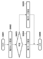
図2は、センサアレイ10を形成する単位センサSの回路構成を例示している。センサSは、例えば、第1部分ps1と第2部分ps2と第3部分ps3とを含みうる。第1部分ps1は、フォトダイオードPDと、トランジスタM1〜M3と、フローティングディフュージョン容量CFD(以下、FD容量CFD)と、感度切り替え用の容量CFD’とを有しうる。フォトダイオードPDは光電変換素子であり、照射された放射線に応じて前述のシンチレータで生じた光を電気信号に変換する。具体的には、当該光に応じた量の電荷がフォトダイオードPDで発生し、発生した電荷量に応じたFD容量CFDの電圧が第2部分ps2に出力される。
FIG. 2 illustrates the circuit configuration of the unit sensors S that form the
また、感度切り替え用の容量CFD’は、センサSの放射線に対する感度を切り替えるために用いられ、トランジスタM1(スイッチ素子)を介してフォトダイオードPDに接続されている。WIDE信号が活性化されることによってトランジスタM1が導通状態になり、FD容量CFDと容量CFD’との合成容量の電圧が第2部分ps2に出力される。このように、センサSでは、容量CFD’を用いるか否かで放射線に対する感度を変更している。また、トランジスタM2は、PRES信号が活性化されることによってフォトダイオードPDの電荷を初期化し、第2部分ps2に出力される電圧をリセットする。 The sensitivity switching capacitor C FD ′ is used to switch the sensitivity of the sensor S to radiation, and is connected to the photodiode PD via the transistor M1 (switch element). When the WIDE signal is activated, the transistor M1 becomes conductive, and the voltage of the combined capacitance of the FD capacitor CFD and the capacitor CFD ′ is output to the second portion ps2. Thus, in the sensor S, the sensitivity to radiation is changed depending on whether or not the capacitor C FD ′ is used. Further, the transistor M2 initializes the charge of the photodiode PD when the PRES signal is activated, and resets the voltage output to the second portion ps2.
第2部分ps2は、トランジスタM3〜M7とクランプ容量CCLと定電流源とを有しうる。トランジスタM3とトランジスタM4と定電流源(例えばカレントミラー構成のトランジスタ)とは電流経路を形成するように直列に接続されている。トランジスタM3のゲートに入力されるイネーブル信号ENが活性化されることによって、第1部分ps1からの電圧を受けるトランジスタM4が動作状態となる。このようにしてソースフォロワ回路が形成され、第1部分ps1からの電圧に応じた電圧が出力される。 The second portion ps2 may have a transistor M3~M7 and the clamp capacitor C CL and the constant current source. The transistor M3, the transistor M4, and a constant current source (for example, a transistor having a current mirror configuration) are connected in series so as to form a current path. When the enable signal EN input to the gate of the transistor M3 is activated, the transistor M4 that receives the voltage from the first portion ps1 is activated. In this way, a source follower circuit is formed, and a voltage corresponding to the voltage from the first portion ps1 is output.
その後段には、トランジスタM5〜7とクランプ容量CCLとで構成されたクランプ回路が設けられている。具体的には、クランプ容量CCLの一方の端子n1が、第1部分ps1のトランジスタM3とトランジスタM4との間のノードに接続されており、他方の端子n2が、クランプスイッチとして機能するトランジスタM5に接続されている。また、トランジスタM6とトランジスタM7と定電流源とは電流経路を形成するように直接に接続されており、当該他方の端子n2は、トランジスタM7のゲートに接続されている。この構成により、第1部分ps1のフォトダイオードPDで生じるkTCノイズ(いわゆるリセットノイズ)が除去される。 The subsequent stage, the clamp circuit is provided which is composed of a transistor M5~7 and the clamp capacitor C CL. Specifically, one terminal n1 of the clamp capacitor C CL, are connected to a node between the transistors M3 and M4 of the first portion ps1, the other terminal n2, functions as a clamp switch transistor M5 It is connected to the. The transistors M6, M7, and the constant current source are directly connected to form a current path, and the other terminal n2 is connected to the gate of the transistor M7. With this configuration, kTC noise (so-called reset noise) generated in the photodiode PD of the first portion ps1 is removed.
具体的には、前述のリセット時における第1部分ps1からの電圧に応じた電圧がクランプ容量CCLの端子n1に入力される。また、クランプ信号PCLが活性化されることによりトランジスタM5が導通状態になり、クランプ電圧VCLがクランプ容量CCLの端子n2に入力される。このようにして、クランプ容量CCLの両端子n1−n2間で生じた電位差をノイズ成分としてクランプし、その後のフォトダイオードPDでの電荷の発生および蓄積に伴う電圧の変化分を信号成分として出力する。 Specifically, a voltage corresponding to the voltage from the first portion ps1 during the aforementioned reset is input to the terminal n1 of the clamp capacitor C CL. The transistor M5 is rendered conductive by the clamp signal PCL is activated, the clamp voltage VCL is supplied to the terminal n2 of the clamp capacitor C CL. In this manner, clamp the potential difference generated between both terminals n1-n2 capacity C CL clamped as a noise component, outputs the variation of the generation and voltage due to charge accumulation in the subsequent photodiode PD as the signal component To do.
また、イネーブル信号ENはトランジスタM6のゲートにも入力され、イネーブル信号ENが活性化されることによってトランジスタM7が動作状態となる。このようにしてソースフォロワ回路が形成され、トランジスタM7のゲート電圧に応じた電圧が第3部分ps3に出力される。 The enable signal EN is also input to the gate of the transistor M6, and the enable signal EN is activated, so that the transistor M7 is activated. In this way, a source follower circuit is formed, and a voltage corresponding to the gate voltage of the transistor M7 is output to the third portion ps3.
第3部分ps3は、トランジスタM8、M10、M11、M13、M14及びM16と、アナログスイッチSW9、SW12及びSW15と、容量CS1、CS2およびCNとを有しうる。 The third portion ps3 can include transistors M8, M10, M11, M13, M14, and M16, analog switches SW9, SW12, and SW15, and capacitors CS1, CS2, and CN.
トランジスタM8と容量CS1とはサンプルホールド回路を形成しており、第2部分ps2からの出力値を保持する保持部として機能する。具体的には、制御信号TS1を用いてトランジスタM8の状態(導通状態または非導通状態)を切り替えることにより、第2部分ps2から得られる信号(光成分にしたがう信号)を容量CS1に保持し、即ち、サンプリングを行う。また、トランジスタM10は、そのソースフォロワ動作によってアンプとして機能し、これによって当該信号は増幅される。当該増幅された信号は、制御信号VSRを用いてアナログスイッチSW9を導通状態にすることより、端子S1から出力される。ここで、トランジスタM8及びM10とアナログスイッチSW10と容量CS1とが形成するユニットを第1のユニットUSH1と称する。 The transistor M8 and the capacitor CS1 form a sample and hold circuit, and function as a holding unit that holds the output value from the second portion ps2. Specifically, by switching the state (conductive state or non-conductive state) of the transistor M8 using the control signal TS1, the signal (the signal according to the light component) obtained from the second part ps2 is held in the capacitor CS1, That is, sampling is performed. Further, the transistor M10 functions as an amplifier by its source follower operation, and thereby the signal is amplified. The amplified signal is output from the terminal S1 by making the analog switch SW9 conductive using the control signal VSR. Here, a unit formed by the transistors M8 and M10, the analog switch SW10, and the capacitor CS1 is referred to as a first unit USH1 .
第1のユニットUSH1と同様にして、トランジスタM11及びM13とアナログスイッチSW12と容量CS2とは、端子S2から信号を出力する第2のユニットUSH2を形成している。例えば、第1のユニットUSH1ではセンサSを第1感度で動作させた場合の信号(第1信号)が保持され、第2のユニットUSH2ではセンサSを第2感度(第1感度とは異なる感度)で動作させた場合の信号(第2信号)が保持される。 Similarly to the first unit USH1 , the transistors M11 and M13, the analog switch SW12, and the capacitor CS2 form a second unit USH2 that outputs a signal from the terminal S2. For example, the first unit U SH1 holds a signal (first signal) when the sensor S is operated at the first sensitivity, and the second unit U SH2 sets the sensor S to the second sensitivity (what is the first sensitivity)? A signal (second signal) when operated at a different sensitivity is held.
また、同様にして、トランジスタM14及びM16とアナログスイッチSW15と容量CNとは、端子Nから信号を出力する第3のユニットUSHNを形成している。なお、後述するが、第3のユニットUSHNでは基準信号が保持され、信号読出部20は、端子S1、S2及びNを介して、第1感度については第1信号と基準信号との差分を読み出し、第2感度については第2信号と基準信号との差分を読み出す。これにより、第2部分ps2に起因する固定パターンノイズ(FPN:Fitted Pattern Noise)が除去される。
Similarly, the transistors M14 and M16, the analog switch SW15, and the capacitor CN form a third unit USHN that outputs a signal from the terminal N. As will be described later, the reference signal is held in the third unit USHN , and the
以下では、図3を参照しながら、動作モードの一例として、動画撮影モードにおけるセンサSの駆動方法の例を述べる。当該動画撮影モードでは、例えば2つの感度で得られる各信号を容量CS1およびCS2に保持し、それぞれ個別に読み出す。例えば、2つの感度で得られた各信号を用いてダイナミックレンジ拡張を行うことも可能である。 Hereinafter, an example of a driving method of the sensor S in the moving image shooting mode will be described as an example of the operation mode with reference to FIG. In the moving image shooting mode, for example, signals obtained with two sensitivities are held in the capacitors CS1 and CS2 and read out individually. For example, it is possible to extend the dynamic range using each signal obtained with two sensitivities.
まず、図3の(A)に例示されるように、時刻t1で動作モード設定および撮影開始設定が為される。その後、時刻t2では撮影のための駆動が開始され、その後、図3の(B)の拡大図に例示されるリセット駆動RDと、図3の(C)の拡大図に例示されるサンプリング駆動SDとが交互に繰り返される。また、サンプリング駆動SDの後(かつ、その次のリセット駆動RDの前)において、センサアレイ10から信号読出を行う読出動作ROが為される。
First, as illustrated in FIG. 3A, operation mode setting and shooting start setting are made at time t1. Thereafter, at time t2, driving for photographing is started, and thereafter, reset driving RD illustrated in the enlarged view of FIG. 3B and sampling driving SD illustrated in the enlarged view of FIG. And are repeated alternately. Further, after the sampling drive SD (and before the next reset drive RD), a read operation RO for reading a signal from the
リセット駆動RDでは、リセット動作と、リセット時の出力成分をノイズ成分としてクランプする動作と、を行う。具体的には、図3の(B)に例示されるように、時刻t2では、イネーブル信号ENをHiレベルにして、トランジスタM3及びM6を導通状態にする。これにより、トランジスタM4及びM7がソースフォロア動作を行う状態になる。 In the reset drive RD, a reset operation and an operation of clamping an output component at the time of reset as a noise component are performed. Specifically, as illustrated in FIG. 3B, at time t2, the enable signal EN is set to Hi level, and the transistors M3 and M6 are turned on. As a result, the transistors M4 and M7 enter a state in which the source follower operation is performed.
時刻t3では、信号PRES及びWIDEをHiレベルにして、感度切替え用のトランジスタM1を導通状態にした状態で、リセット用のトランジスタM2を導通状態にする。これにより、フォトダイオードPDは基準電圧VRESに接続され、フォトダイオードPDがリセットされると共に容量CFD’の電圧もリセットされる。また、リセット直後のトランジスタM4のゲート電圧に応じた電圧が、クランプ容量CCLの一方の端子n1(トランジスタM4側の端子)に入力される。 At time t3, the signals PRES and WIDE are set to the Hi level, the sensitivity switching transistor M1 is turned on, and the reset transistor M2 is turned on. Thus, the photodiode PD is connected to the reference voltage VRES, the voltage of the capacitor C FD 'with the photodiode PD is reset is reset. Further, a voltage corresponding to the gate voltage of the transistor M4 immediately after reset is input to one terminal n1 (transistor M4 side terminal) of the clamp capacitor C CL.
時刻t4では、信号PCLをHiレベルにして、前述のクランプを行うためのトランジスタM5を導通状態にする。これにより、クランプ電圧VCLがクランプ容量CCLの他方の端子n2(トランジスタM7側の端子)に入力される。 At time t4, the signal PCL is set to the Hi level, and the transistor M5 for performing the above-described clamping is turned on. Accordingly, the clamp voltage VCL is supplied to the other terminal n2 (transistors M7 side terminal) of the clamp capacitor C CL.
また、時刻t4では、信号TS1、TS2およびTNをHiレベルにして、前述のサンプリングを行うためのトランジスタM8、M11およびM14を導通状態にする。これにより、容量CS1、CS2およびCNはいずれも初期状態(トランジスタM7のゲート電圧が基準電圧VCLのときの第2部分ps2の出力値の電圧)になる。 At time t4, the signals TS1, TS2, and TN are set to the Hi level, and the transistors M8, M11, and M14 for performing the above-described sampling are turned on. As a result, the capacitors CS1, CS2, and CN are all in the initial state (the voltage of the output value of the second portion ps2 when the gate voltage of the transistor M7 is the reference voltage VCL).
時刻t5では、信号PRES及びWIDEをLowレベルにして、トランジスタM1及びM2を非導通状態にする。これにより、容量CFD’は、トランジスタM1が非導通状態になるため、リセット直後の電圧で固定され、また、クランプ容量CCLの端子n1は、リセット直後のトランジスタM4のゲート電圧に応じた電圧にセットされる。 At time t5, the signals PRES and WIDE are set to low level, and the transistors M1 and M2 are turned off. As a result, the capacitor C FD ′ is fixed at the voltage immediately after the reset because the transistor M1 is in a non-conductive state, and the terminal n1 of the clamp capacitor C CL is a voltage corresponding to the gate voltage of the transistor M4 immediately after the reset. Set to
時刻t6では、信号PCLをLowレベルにして、トランジスタM5を非導通状態にする。これにより、端子n1と端子n2との電位差(基準電圧VRESにしたがう電圧と基準電圧VCLとの電位差)に応じた電荷がクランプ容量CCLに保持され、前述のkTCノイズのクランプが完了する。 At time t6, the signal PCL is set to low level, and the transistor M5 is turned off. Accordingly, charge corresponding to the potential difference between the terminal n1 and the terminal n2 (potential difference between the voltage according to the reference voltage VRES and the reference voltage VCL) is held by the clamp capacitance C CL, is completed clamp of the aforementioned kTC noise.
また、時刻t6では、信号TS1、TS2およびTNをLowレベルにして、トランジスタM8、M11およびM14を非導通状態にする。これにより、容量CS1、CS2およびCNの電圧が固定される。 At time t6, the signals TS1, TS2, and TN are set to the low level, and the transistors M8, M11, and M14 are turned off. Thereby, the voltages of the capacitors CS1, CS2 and CN are fixed.
また、時刻t6では、前述の曝射許可信号114をHiレベル(許可状態)にする。その後、フォトダイオードPDでは電荷が発生し蓄積される。
At time t6, the above-mentioned
時刻t7では、イネーブル信号ENをLowレベルにして、トランジスタM3及びM6を非導通状態にする。これにより、トランジスタM4及びM7を非動作状態にする。 At time t7, the enable signal EN is set to Low level, and the transistors M3 and M6 are turned off. This puts the transistors M4 and M7 into a non-operating state.
以上のようにして、リセット駆動RDの一連の動作が終了する。即ち、リセット駆動RDでは、フォトダイオードPDをリセットすると共に、第1部分ps1のフォトダイオードPDに起因するkTCノイズに相当する電圧がクランプ容量CCLに保持され、また、容量CS1、CS2およびCNが初期化される。 As described above, a series of operations of the reset driving RD is completed. That is, the reset driving RD, resets the photodiode PD, a voltage corresponding to the kTC noise caused by the photodiode PD of the first portion ps1 is held by the clamp capacitance C CL, The capacitor CS1, CS2 and the CN It is initialized.
なお、リセット駆動RDは、全てのセンサについて一括で為され、その後(例えば時刻t31〜t32)に為されるリセット駆動RDも上述と同様のタイミングで為されうる。また、制御タイミングのずれを防ぐことによって隣接画素間でデータの連続性が維持されうる。 Note that the reset driving RD is performed for all the sensors at once, and the reset driving RD performed thereafter (for example, at times t31 to t32) can also be performed at the same timing as described above. Further, data continuity can be maintained between adjacent pixels by preventing a shift in control timing.
次に、サンプリング駆動SDでは、センサSを2つの感度で駆動し、各感度で得られる信号を容量CS1およびCS2に保持する動作を行う。具体的には、図3の(C)に例示されるように、時刻t11でイネーブル信号ENをHiレベルにしてトランジスタM3及びM6を導通状態にし、トランジスタM4及びM7がソースフォロア動作を行う状態になる。なお、時刻t11では信号WIDEはLowレベルであり、センサSは、第1感度に対応する高感度モードになっている。 Next, in the sampling drive SD, the sensor S is driven with two sensitivities, and an operation of holding signals obtained with the respective sensitivities in the capacitors CS1 and CS2. Specifically, as illustrated in FIG. 3C, at time t11, the enable signal EN is set to the Hi level so that the transistors M3 and M6 are turned on, and the transistors M4 and M7 perform the source follower operation. Become. At time t11, the signal WIDE is at the low level, and the sensor S is in the high sensitivity mode corresponding to the first sensitivity.
トランジスタM4のゲート電圧(即ち、FD容量CFDの電圧)は、フォトダイオードPDで発生し蓄積された電荷量に応じて変化しており、当該変化したゲート電圧に応じた電圧がクランプ容量CCLの一方の端子n1に入力され、端子n1の電位が変化する。クランプ容量CCLの他方の端子n2の電位変化は、当該端子n1の電位変化にしたがう。ここで、前述のとおり、クランプ容量CCLにはkTCノイズに相当する電圧が保持されているため、この電位変化の量が信号成分として第3部分ps3に出力される。 The gate voltage of the transistor M4 (that is, the voltage of the FD capacitor C FD ) changes according to the amount of charge generated and accumulated in the photodiode PD, and the voltage according to the changed gate voltage is the clamp capacitor C CL The potential of the terminal n1 changes. Potential change of the other terminal n2 of the clamp capacitor C CL is in accordance with the potential change of the terminal n1. Here, as described above, the voltage corresponding to the kTC noise is held in the clamp capacitor C CL, the amount of the potential change is output as a signal component in the third part ps3.
時刻t12では、信号TS1をHiレベルにしてトランジスタM8を導通状態にし、即ち、上述の高感度モードにおける第2部分ps2の出力値についてのサンプリングを開始する。具体的には、容量CS1は、時刻t11の駆動にしたがう第2部分ps2の出力値の電圧(トランジスタM7のゲート電圧に応じた電圧)になる。次に、時刻t13では、時刻t12でサンプリングを開始したので、曝射許可信号114をLowレベル(禁止状態)にする。その後、時刻t14では、信号TS1をLowレベルにしてトランジスタM8を非導通状態にし、即ち、第2部分ps2の出力値をホールドする。具体的には、容量CS1の電圧が第2部分ps2の出力値で固定される。
At time t12, the signal TS1 is set to Hi level to turn on the transistor M8, that is, sampling of the output value of the second portion ps2 in the high sensitivity mode described above is started. Specifically, the capacitor CS1 becomes the voltage of the output value of the second portion ps2 according to the driving at time t11 (the voltage corresponding to the gate voltage of the transistor M7). Next, at time t13, since sampling is started at time t12, the
即ち、時刻t12〜t14では、第1感度で得られた第1信号が、第1のユニットUSH1の保持部(容量CS1)に保持される。 That is, at time T12~t14, the first signal obtained in the first sensitivity is held in the holding portion of the first unit U SH1 (capacity CS1).
次に、時刻t15では、信号WIDEをHiレベルとして、感度切替え用のトランジスタM1を導通状態にする。これにより、トランジスタM1を介して容量CFD’がフォトダイオードPDに電気的に接続され、トランジスタM4のゲート電圧は、FD容量CFDと容量CFD’との合成容量の電圧となる。当該合成容量の値は、FD容量CFDの値よりも大きいため、トランジスタM4のゲート電圧が変化しにくくなり、即ち、センサSは、第2感度に対応する低感度モードに切り替わる。一方で、フォトダイオードPDの電荷を、さらに読み出すことが可能になる。 Next, at time t15, the signal WIDE is set to Hi level, and the sensitivity switching transistor M1 is turned on. As a result, the capacitor C FD ′ is electrically connected to the photodiode PD via the transistor M1, and the gate voltage of the transistor M4 becomes a voltage of the combined capacitor of the FD capacitor C FD and the capacitor C FD ′. Value of the combined capacitance is larger than the value of the FD capacitance C FD, becomes the gate voltage of the transistor M4 is hardly changed, i.e., the sensor S is switched to the low-sensitivity mode corresponding to the second sensitivity. On the other hand, the charge of the photodiode PD can be further read out.
時刻t16では、信号TS2をHiレベルにしてトランジスタM11を導通状態にし、即ち、上述の低感度モードにおける第2部分ps2の出力値についてのサンプリングを開始する。具体的には、容量CS2は、時刻t15の駆動にしたがう第2部分ps2の出力値の電圧(トランジスタM7のゲート電圧に応じた電圧)になる。その後、時刻t17では、信号TS2をLowレベルにしてトランジスタM11を非導通状態にし、即ち、第2部分ps2の出力値をホールドする。具体的には、容量CS2の電圧が第2部分ps2の出力値で固定される。 At time t16, the signal TS2 is set to Hi level to turn on the transistor M11, that is, sampling of the output value of the second portion ps2 in the low sensitivity mode described above is started. Specifically, the capacitor CS2 becomes the voltage of the output value of the second portion ps2 according to the driving at time t15 (voltage corresponding to the gate voltage of the transistor M7). Thereafter, at time t17, the signal TS2 is set to a low level to turn off the transistor M11, that is, hold the output value of the second portion ps2. Specifically, the voltage of the capacitor CS2 is fixed at the output value of the second portion ps2.
即ち、時刻t16〜t17では、第2感度で得られた第2信号が、第2のユニットUSH2の保持部(容量CS2)に保持される。 That is, at time t16 to t17, the second signal obtained in the second sensitivity is held in the holding portion of the second unit U SH2 (capacity CS2).
次に、時刻t18では、信号PRESをHiレベルにして、リセット用のトランジスタM2を導通状態にする。これにより、FD容量CFD及び容量CFD’の電圧をリセットして基準電圧VRESにし、端子n1の電圧も時刻t3と同じ状態にリセットされる。 Next, at time t18, the signal PRES is set to Hi level, and the resetting transistor M2 is turned on. As a result, the voltages of the FD capacitor C FD and the capacitor C FD ′ are reset to the reference voltage VRES, and the voltage at the terminal n1 is also reset to the same state as at time t3.
時刻t19では、信号PCLをHiレベルにしてトランジスタM5を導通状態にし、クランプ電圧VCLがクランプ容量CCLの他方の端子n2(トランジスタM7側の端子)に入力される。 At time t19, and the signal PCL to Hi level the transistor M5 in the conductive state, the clamp voltage VCL is supplied to the other terminal n2 (transistors M7 side terminal) of the clamp capacitor C CL.
時刻t20では、信号PRES及びWIDEをLowレベルにしてトランジスタM1及びM2を非導通状態にする。これにより、容量CFD’はリセット直後の電圧で固定され、また、クランプ容量CCLの端子n1は、リセット直後のトランジスタM4のゲート電圧に応じた電圧にセットされる。 At time t20, the signals PRES and WIDE are set to a low level, and the transistors M1 and M2 are turned off. As a result, the capacitor C FD ′ is fixed at the voltage immediately after reset, and the terminal n1 of the clamp capacitor C CL is set to a voltage corresponding to the gate voltage of the transistor M4 immediately after reset.
時刻t21では、信号TNをHiレベルにしてトランジスタM14を導通状態にする。これにより、容量CNは充電され、トランジスタM7のゲート電圧が基準電圧VCLのときの第2部分ps2の出力値の電圧になる。時刻t22では、信号TNをLowレベルにしてトランジスタM14を非導通状態にする。これにより、容量CNの電圧が固定される。 At time t21, the signal TN is set to Hi level, and the transistor M14 is turned on. Thereby, the capacitor CN is charged, and becomes the voltage of the output value of the second part ps2 when the gate voltage of the transistor M7 is the reference voltage VCL. At time t22, the signal TN is set to the low level to turn off the transistor M14. Thereby, the voltage of the capacitor CN is fixed.
即ち、時刻t21〜t22では、第2部分ps2の回路構成に依存する熱ノイズ、1/fノイズ、温度差、プロセスばらつき等の固定パターンノイズに相当する電圧が容量CNに保持される。 That is, at time t21 to t22, a voltage corresponding to fixed pattern noise such as thermal noise, 1 / f noise, temperature difference, process variation, etc. depending on the circuit configuration of the second portion ps2 is held in the capacitor CN.
最後に、時刻t23では信号PCLをLowレベルにしてトランジスタM5を非導通状態にし、時刻t24ではイネーブル信号ENをLowレベルにしてトランジスタM3及びM6を非導通状態(トランジスタM4及びM7を非動作状態)にする。 Finally, at time t23, the signal PCL is set to low level to turn off the transistor M5, and at time t24, the enable signal EN is set to low level to turn off the transistors M3 and M6 (transistors M4 and M7 are in a non-operating state). To.
以上のようにして、サンプリング駆動SDの一連の動作が終了する。即ち、サンプリング駆動SDでは、センサSの各感度で得られる信号が容量CS1およびCS2に保持されると共に、第2部分ps2に起因する固定パターンノイズに相当する電圧が容量CNに保持される。 As described above, a series of operations of the sampling drive SD is completed. That is, in the sampling drive SD, signals obtained with the respective sensitivities of the sensor S are held in the capacitors CS1 and CS2, and a voltage corresponding to the fixed pattern noise caused by the second portion ps2 is held in the capacitor CN.
なお、サンプリング駆動SDは、前述のリセット駆動RDと同様に、各センサユニット120の制御タイミングのずれを防ぐため、全てのセンサについて一括で為されうる。例えば、この後(例えば時刻t41〜t43)に為されるサンプリング駆動SDも、上述と同様のタイミングで為されうる。
Note that the sampling drive SD can be performed collectively for all sensors in order to prevent a shift in the control timing of each
次に、図4を参照しながら、前述の各センサユニット120の構成例を述べる。前述のとおり、複数のセンサユニット120が基台の上にタイリングされることによって大型のセンサパネル105が形成されうる。各センサユニット120は、m行×n列で配列された複数のセンサSと、各センサSを駆動するための垂直走査回路403と、各センサSから信号読出を行うための水平走査回路404と、を備える。
Next, a configuration example of each
垂直走査回路403および水平走査回路404は、例えばシフトレジスタで構成されており、制御部109からの制御信号に基づいて動作する。垂直走査回路403は、制御線405を介して各センサSに制御信号を入力し、当該制御信号に基づいて各センサSを行単位で駆動する。例えば、垂直走査回路403は行選択部として機能し、信号読出を行うべきセンサSを行ごとに選択する。また、水平走査回路404は列選択部として機能し、制御信号に基づいて各センサSを列ごとに選択して、当該各センサSからの信号を順に出力させる(水平転送)。ここで、行選択部(垂直走査回路404)の動作周波数は、列選択部(水平走査回路404)の動作周波数に比べて大きく、即ち、行選択部(垂直走査回路404)は列選択部(水平走査回路404)に比べて動作が遅い。
The
また、各センサユニット120は、各センサSの容量CS1に保持された第1信号を読み出すための端子ES1と、容量CS2に保持された第2信号を読み出すための端子ES2と、容量CNに保持された電圧を読み出すための端子ENと、を有する。また、各センサユニット120はセレクト端子ECSをさらに有し、端子ECSが受ける信号が活性化されることによって、当該センサユニット120の各センサSの信号が、端子ES1、ES2及びENを介して読み出されうる。
Furthermore, each
具体的には、前述の各センサSの端子S1、S2及びNは、各端子に対応する列信号線406〜408に接続されている。当該列信号線406〜408は、水平走査回路404からの制御信号に応答して導通状態になるスイッチSWHを介して、アナログ出力線409〜411に接続されている。当該アナログ出力線409〜411の信号は、端子ECSが受ける信号に応答して導通状態になるスイッチSWCSを介して、端子ES1、ES2及びENから出力される。
Specifically, the terminals S1, S2, and N of each sensor S described above are connected to
また、各センサユニット120は、垂直走査回路403および水平走査回路404を制御するための各制御信号を受ける端子HST、CLKH、VSTおよびCLKVをさらに有する。端子HSTは、水平走査回路404に入力されるスタートパルスを受ける。端子CLKHは、水平走査回路404に入力されるクロック信号を受ける。端子VSTは、垂直走査回路403に入力されるスタートパルスを受ける。端子CLKVは、垂直走査回路403に入力されるクロック信号を受ける。これらの各制御信号は、制御部109から入力される。
Each
以上に例示された構成により、センサユニット120では、各センサSは行単位で制御され、各保持部に保持された信号が列単位で出力され(水平転送が為され)、信号読出が為される。
With the configuration exemplified above, in the
図5は、信号読出部20の回路構成を例示しており、信号読出部20は、例えば差動アンプ等を含む信号増幅部107とAD変換を行うAD変換部108とを有しうる。端子ES1からの信号は、端子TRO1からの制御信号に応答して導通状態になるスイッチM50を介して、信号増幅部107の反転入力端子に入力される。また、端子ES2からの信号は、端子TRO2からの制御信号に応答して導通状態になるスイッチM51を介して、当該反転入力端子に入力される。スイッチM50及びM51は、端子ES1及び端子ES2の一方の信号が当該反転入力端子に入力されるように制御される。なお、スイッチM50及びM51並びに信号増幅部107は、信号ADCLKの周期に追従可能な応答特性を有するように設計されればよい。
FIG. 5 illustrates a circuit configuration of the
また、端子ENからの信号は信号増幅部107の非反転入力端子に入力される。信号増幅部107では、端子ES1からの信号と端子ENからの信号との差分、又は端子ES2からの信号と端子ENからの信号との差分が増幅され、当該差分はAD変換部108でADCLK端子を介して入力されるクロック信号に基づいてAD変換される。このような構成により、前述の固定パターンノイズが除去されると共に、センサユニット120の画像データ(デジタルデータ)が得られ、ADOUT端子を介して制御部109に出力される。
The signal from the terminal E N is input to the non-inverting input terminal of the
以下、図6を参照しながら、本実施形態にかかる信号読出のための撮像装置100の制御方法を述べる。図6は、制御用の各端子(VST、CLKV、TRO1、TRO2、HST、CLKHおよびADCLK)に入力される制御信号について、信号読出を行うためのタイミングチャートを例示している。なお、センサユニット120から信号読出を行う際は、当該センサユニット120の端子ECSにはHiレベルが入力され、スイッチSWCSは導通状態になっている。
Hereinafter, a method for controlling the
以下では、各端子に入力される制御信号を、単に「信号」と称し、端子の記号を付して表す。例えば、端子VSTに入力される制御信号を信号VSTと示す(他の制御信号についても同様とする)。 Hereinafter, the control signal input to each terminal is simply referred to as a “signal” and is represented by a terminal symbol. For example, a control signal input to the terminal VST is indicated as a signal VST (the same applies to other control signals).
図6の(A)に示されるように、時刻t100では信号VSTをHiレベルにする(端子VSTでスタートパルスを受ける。)これにより、第1行目のセンサSが垂直走査回路403により選択されるようにセットされる。その後、時刻t130までクロック信号CLKVを受け、垂直走査回路403は、クロック信号CLKVを受けるたびに、選択している行を、第1行目から第m行目まで順にシフトさせる。即ち、時刻t100〜t130では、各センサSが、第1行目から第m行目まで行ごとに順に選択される。
As shown in FIG. 6A, at time t100, the signal VST is set to the Hi level (a start pulse is received at the terminal VST). As a result, the sensor S in the first row is selected by the
また、水平走査回路404は、垂直走査回路403により1行分の各センサSが選択されている間(例えば時刻t110〜t120の間)に、当該各センサSを第1列目から第n列目まで列ごとに選択して順に信号を出力させる。即ち、例えば時刻t110〜t120では、水平走査回路404は第1行目の各センサSの信号の水平転送を行う。具体的には、図6の(B)に示例されるシーケンスが為される。
Further, the
まず、時刻t110でクロック信号CLKVを受けた後、時刻t111では端子HSTでスタートパルスを受ける(時刻t111〜t112にわたって信号HSTをHiレベルにする)。これにより、第1行目の各センサSのうち、第1列目のセンサSが水平走査回路404により選択されるようにセットされる。
First, after receiving the clock signal CLKV at time t110, a start pulse is received at the terminal HST at time t111 (the signal HST is set to Hi level from time t111 to t112). Thereby, among the sensors S in the first row, the sensor S in the first column is set to be selected by the
その後、時刻t120までクロック信号CLKHを受け、水平走査回路404は、クロック信号CLKHを受けるたびに、選択している列を、第1列目から第n列目まで順にシフトさせる。ここで、ある列のセンサSが水平走査回路404によって選択されることにより、前述のスイッチSW9、SW12及びSW15が導通状態になり、前述の保持部(容量CS1等)の信号が、対応する列信号線406〜408にそれぞれ出力される。当該列のセンサSが水平走査回路404により選択されている間に、当該センサSから出力された信号が読み出される。
Thereafter, the clock signal CLKH is received until time t120, and the
例えば、時刻t113では、クロック信号CLKHをHiレベルにして、第1行目・第1列目のセンサSを選択すると共に、信号TRO1をHiレベルにして当該センサSの第1信号(容量CS1の信号)を出力する。その後、時刻t114では、クロック信号CLKHをLowレベルにすると共に、信号ADCLKをHiレベルにして当該第1信号についてのAD変換を行う。次に、時刻t115では、信号TRO1をLowレベルにすると共に信号TRO2をHiレベルにして当該センサSの第2信号(容量CS2の信号)を出力する。その後、時刻t116では、信号ADCLKをHiレベルにして当該第2信号についてのAD変換を行う。なお、前述のとおり、これらのAD変換は、固定パターンノイズを除去するため、基準信号(容量CNの信号)との差分について為される。 For example, at time t113, and the clock signal CLKH to Hi level, thereby selecting the sensor S of the first row - first column, first signal of the sensor S and the signal T RO1 to Hi level (capacity CS1 Output signal). Thereafter, at time t114, the clock signal CLKH is set to the Low level and the signal ADCLK is set to the Hi level to perform AD conversion on the first signal. Next, at time t115, the signal T RO2 with the signal T RO1 to Low level in the Hi level to output a second signal (signal capacity CS2) of the sensor S. Thereafter, at time t116, the signal ADCLK is set to the Hi level, and AD conversion is performed on the second signal. As described above, these AD conversions are performed on a difference from the reference signal (capacitor CN signal) in order to remove fixed pattern noise.
即ち、時刻t113〜t116では、垂直走査回路403により選択されている第1行目の各センサSのうち、第1列目のセンサSが水平走査回路404により選択され、当該センサSの第1信号および第2信号がそれぞれ出力され、AD変換が為される。その結果、第1行目・第1列目のセンサSから、第1感度および第2感度のそれぞれについてのデジタル信号が得られる。
That is, from time t113 to t116, among the sensors S in the first row selected by the
その後、第2列目〜第n列目についても同様の制御を行って、時刻t120までに、第1行目についての1行分のデジタルデータ(第1感度及び第2感度のそれぞれについてのデジタルデータ)が得られる。 Thereafter, the same control is performed for the second column to the n-th column, and by time t120, one row of digital data (digital for each of the first sensitivity and the second sensitivity) is obtained for the first row. Data).
以上のシーケンスを第2行目〜第m行目の各行についても同様にして行い、全てのセンサSからの信号読出が完了する。読み出されたデジタルデータは、順次、画像データとして制御部109に出力され、制御部109ないし処理部101で所定の信号処理を経て、放射線画像として表示部102に表示されうる。ここで、制御部109に出力されたデジタルデータは、信号読出部20で読み出された順番で、画像データインターフェース111により処理部101に送信されうる。
The above sequence is similarly performed for each of the second to m-th rows, and signal reading from all the sensors S is completed. The read digital data is sequentially output to the
以上では、第1感度および第2感度で取得した信号の両方を読み出した。これにより、一方の信号を選択的に用いて放射線画像を生成してもよいし、当該一方の信号を出力できない場合には他方の信号を当該一方の信号の代わりに用いてもよいし、また、両方の信号を用いてもよい。なお、一方の信号を選択的に用いる動作モードにおいて、当該一方の信号を出力できない場合には、他方の信号をゲイン調整等によって補正して、当該一方の信号の代わりに用いてもよい。また、両方の信号を用いる場合には、例えばダイナミックレンジ拡張を行ってもよい。この時、第2感度のデジタルデータが欠陥であり、第1感度のデジタルデータが正常であった場合、飽和領域でなければ第1感度のデジタルデータをゲイン比で補正したデジタルデータを、第2感度の欠陥補正デジタルデータの代わりに使用する。また、第1感度のデジタルデータが欠陥で、第2感度のデジタルデータが正常であった場合も、ノイズ領域でなければ第2感度のデジタルデータをゲイン比で補正したデジタルデータを、第1感度の欠陥補正デジタルデータの代わりに使用する。これにより、欠陥画素を周辺画素で補正するよりも正確な欠陥画素補正を行うことができる。 In the above, both signals acquired with the first sensitivity and the second sensitivity are read out. Accordingly, a radiographic image may be generated by selectively using one of the signals, and when the one signal cannot be output, the other signal may be used instead of the one signal. Both signals may be used. In an operation mode in which one signal is selectively used, when the one signal cannot be output, the other signal may be corrected by gain adjustment or the like and used instead of the one signal. Further, when both signals are used, for example, dynamic range expansion may be performed. At this time, when the digital data of the second sensitivity is defective and the digital data of the first sensitivity is normal, the digital data obtained by correcting the digital data of the first sensitivity with the gain ratio is not the saturation region, Use in place of sensitivity defect correction digital data. Further, even when the first sensitivity digital data is defective and the second sensitivity digital data is normal, the digital data obtained by correcting the second sensitivity digital data with the gain ratio is converted into the first sensitivity if it is not a noise region. Used instead of defect correction digital data. This makes it possible to perform defective pixel correction more accurately than correcting defective pixels with peripheral pixels.
ここで、垂直走査回路403が制御線405を介して制御信号を出力して「行」を選択することにより、制御線405と交差する列信号線406〜408ではノイズ等に起因する電位変動が生じる。よって、信号読出は、この電位変動が収まった後に(即ち、「行」の選択が為されてから所定期間が経過した後に)為される必要があり、このことは読出時間の増大をもたらしうる。特に、多画素化に伴って、行数が増大し、また、各列信号線の配線容量も大きくなるため、この影響は顕著になる。
Here, when the
本実施形態では、ある行の各センサSについての第1信号および第2信号の読み出しを行った後に、次の行の各センサSについての第1信号および第2信号の読み出しを行う。よって、本実施形態の信号読出の方法によれば、垂直走査回路403が「行」を選択する回数(以下、行選択回数と称する)はm回である。
In the present embodiment, after reading the first signal and the second signal for each sensor S in a certain row, the first signal and the second signal for each sensor S in the next row are read. Therefore, according to the signal reading method of the present embodiment, the number of times the
例えば、参考例として、全ての行で第1信号についての信号読出を行った後に、全ての行で第2信号についての信号読出を行う場合は、行選択回数はm×2回となってしまうため、本実施形態によると、この参考例よりも行選択回数を低減させることができる。即ち、本実施形態によると、複数の感度で得られた各信号をそれぞれ読み出すのに際して、信号読出の高速化という点で有利である。 For example, as a reference example, when signal readout for the first signal is performed in all rows and then signal readout for the second signal is performed in all rows, the number of row selections is m × 2 times. Therefore, according to the present embodiment, the number of row selections can be reduced as compared with this reference example. That is, according to the present embodiment, when reading each signal obtained with a plurality of sensitivities, it is advantageous in terms of speeding up the signal reading.
なお、以上では、信号読出部20は、図5に示されるように、信号増幅部107およびAD変換部108を有し、容量CS1の第1信号と容量CS2の第2信号とについて順にAD変換を行う構成を例示したが、本発明はこの構成に限られるものではない。例えば、信号読出部20は、図7に例示されるように、第1信号及び第2信号のそれぞれに対応するように、信号増幅部107a及び107bとAD変換部108a及び108bとをそれぞれ設けてもよい。この構成によると、第1信号および第2信号の読み出し(出力およびAD変換)を並列に行うことが可能であり、信号読出の高速化に有利である。
In the above, as shown in FIG. 5, the
(第2実施形態)
図8を参照しながら、第2実施形態を説明する。前述の第1実施形態では、ある列のセンサSからの第1信号および第2信号の読み出しを行った後に、次の列のセンサSからの第1信号および第2信号の読み出しを行う場合を例示した。しかしながら、本発明は、ある行の各センサSについての第1信号および第2信号の読み出しを行った後に、次の行の各センサSについての第1信号および第2信号の読み出しを行えばよく、この構成に限られない。本実施形態では、ある行の各センサSから第1信号を読み出した後に、当該行の各センサSから第2信号を読み出し、その後、次の行の各センサSについての信号読出を行う。
(Second Embodiment)
The second embodiment will be described with reference to FIG. In the first embodiment described above, the first signal and the second signal are read from the sensor S in the next column after the first signal and the second signal are read from the sensor S in a certain column. Illustrated. However, in the present invention, after reading the first signal and the second signal for each sensor S in a certain row, the first signal and the second signal for each sensor S in the next row may be read. The configuration is not limited to this. In the present embodiment, after reading the first signal from each sensor S in a certain row, the second signal is read from each sensor S in that row, and then the signal is read out from each sensor S in the next row.
図8は、本実施形態にかかる信号読出のための撮像装置100の制御方法を説明するためのタイミングチャートを、図6と同様にして例示している。第1実施形態と異なる主な点は、信号TRO1及びTRO2の波形である。即ち、第1行目の各センサSから信号を読み出す時刻t210〜t220の間のうち、前半では各センサSからの第1信号の読み出しを行い、後半では当該各センサSからの第2信号の読み出しを行う。また、この制御方法に伴って、信号HST及びADCLKの波形を第1実施形態(図6)から変更している。
FIG. 8 illustrates a timing chart for explaining a control method of the
具体的には、以下のシーケンスにしたがう。まず、時刻t200において端子VSTでスタートパルスを受けた後、時刻t210でクロック信号CLKVを受けて第1行目の各センサSが選択される。その後、時刻t211〜t215にわたって信号TRO1をHiレベルにし、信号TRO2をLowレベルにする。これにより、当該各センサSの第1信号が出力される状態になる。 Specifically, the following sequence is followed. First, after receiving a start pulse at terminal VST at time t200, each sensor S in the first row is selected in response to clock signal CLKV at time t210. Then, the signal T RO1 to Hi level over time T211~t215, the signal T RO2 to Low level. As a result, the first signal of each sensor S is output.
時刻t211において端子HSTでスタートパルスを受けた後、時刻t212でクロック信号CLKHを受ける。第1実施形態でも述べたように、水平走査回路404は、クロック信号CLKHを受けるたびに、選択している列を、第1列目から第n列目まで順にシフトさせる。各クロック信号CLKHの間(例えば、時刻t213)では信号ADCLKが入力され、これにより、選択されている列におけるセンサSからの第1信号についてのAD変換が為される。その後、例えば時刻t214で、次の列のセンサSが選択され、当該センサSについての第1信号の出力およびAD変換が同様にして為される。このようにして、第1信号の読出動作が第1列目から第n列目まで順に列ごとに為される。その後、時刻t215では、信号TRO1をLowレベルにし、信号TRO2をHiレベルにして、第1列目から第n列目まで順に列ごとに、第2信号の読出動作を同様の手順で行う。ここで、制御部109に出力されたデジタルデータは、信号読出部20で読み出された順番で、センサパネル105の行ごとに画像データインターフェース111により処理部101に送信されうる。
After receiving a start pulse at the terminal HST at time t211, the clock signal CLKH is received at time t212. As described in the first embodiment, each time the
本実施形態によると、ある行の各センサSから第1信号を読み出した後に、当該行の各センサSから第2信号を読み出し、その後、次の行の各センサSについての信号読出を行う。このような制御方法によっても、垂直走査回路403による行選択回数はm回であり、第1実施形態と同様の効果が得られる。この制御方法は、例えば、信号の読み出し速度が、信号増幅部107の動作速度に律速される場合や、信号ADCLK、若しくは信号TRO1及びTRO2の周波数に律速される場合に有利である。
According to the present embodiment, after reading the first signal from each sensor S in a certain row, the second signal is read from each sensor S in that row, and then the signal is read out from each sensor S in the next row. Even with such a control method, the number of row selections by the
(第3実施形態)
図9乃至11を参照しながら、第3実施形態を説明する。前述の各実施形態では、2つの感度で得られる2つの信号のそれぞれを順に読み出す場合を例示した。しかし、この信号読出は、動作モードに応じて為されればよく、他の動作モードでは2つの信号のうちの一方のみが読み出されてもよい。
(Third embodiment)
The third embodiment will be described with reference to FIGS. In each of the above-described embodiments, the case where each of two signals obtained with two sensitivities is sequentially read is illustrated. However, this signal reading may be performed according to the operation mode, and only one of the two signals may be read in the other operation modes.
図9は、複数の動作モードにしたがう撮像装置100の動作のフローチャートを例示している。撮像装置100は、動作モードとして、2つの信号の一方のみを読み出す第1モードと、2つの信号の両方を読み出す第2モード(例えばダイナミックレンジ拡張を行うモード)とを有しうる。
FIG. 9 illustrates a flowchart of the operation of the
まず、ステップS901(以下、単に「S901」とし、他のステップについても同様とする。)では、動作モードの設定が開始される。次に、S902では、制御部109は、制御用インターフェース110を介して、設定情報ないし撮影情報を処理部101から受ける。S903では、処理部101からの設定情報ないし撮影情報に基づいて、動作モードを判定する。この判定結果に基づいて、S904で第1モードを設定し、又は、S905で第2モードを設定する。最後に、S906で動作モードの設定を完了する。
First, in step S901 (hereinafter simply referred to as “S901” and the same applies to other steps), setting of the operation mode is started. In step S <b> 902, the
図10は、各センサSから2つの信号の一方のみを読み出す第1モードにおけるセンサSの駆動方法を例示している。第1モードでは、第1感度及び第2感度の一方について、前述の第1実施形態(図3)と同様の手順で各センサSを駆動すればよい。具体的には、サンプリング駆動SDにおいて、信号WIDEをHiレベル及びLowレベルの一方に固定した状態で、信号TS1及びTS2の少なくとも一方を駆動すればよい。 FIG. 10 illustrates a method for driving the sensor S in the first mode in which only one of the two signals is read from each sensor S. In the first mode, each sensor S may be driven in the same procedure as in the first embodiment (FIG. 3) for one of the first sensitivity and the second sensitivity. Specifically, in the sampling drive SD, at least one of the signals TS1 and TS2 may be driven in a state where the signal WIDE is fixed to one of the Hi level and the Low level.
例えば、信号WIDEは、高感度モードではLowレベルに固定し、低感度モードではHiレベルに固定すればよい。信号TS1及びTS2は、一方のみを活性化させてもよいし、両方を活性化させてもよい。ここでは、両方を活性化させる場合を例示しているが、この場合は、それにより得られる2つの信号は互いに同じ信号レベルである。なお、リセット駆動RDについては、前述の第1実施形態と同様にすればよい。 For example, the signal WIDE may be fixed at the Low level in the high sensitivity mode and fixed at the Hi level in the low sensitivity mode. Only one of the signals TS1 and TS2 may be activated, or both may be activated. Here, a case where both are activated is illustrated, but in this case, two signals obtained thereby have the same signal level. The reset drive RD may be the same as that in the first embodiment.
より具体的には、時刻t301〜t305にわたってイネーブル信号ENをHiレベルにし、その間の時刻t302〜t303で信号TS1及びTS2をHiレベルにする。これにより、容量CS1及びCS2には同じレベルの信号が保持される。その後の時刻t304〜t305では、前述の第1実施形態と同様にして、固定パターンノイズを除去するための基準信号が容量CNに保持される。 More specifically, the enable signal EN is set to Hi level from time t301 to t305, and the signals TS1 and TS2 are set to Hi level at times t302 to t303 during that time. As a result, signals of the same level are held in the capacitors CS1 and CS2. At subsequent times t304 to t305, the reference signal for removing the fixed pattern noise is held in the capacitor CN as in the first embodiment described above.
図11は、上述の第1モードで得られた信号の信号読出のための撮像装置100の制御方法を説明するためのタイミングチャートを例示している。ここでは図示しないが、信号TRO1及びTRO2については、2つの保持部(容量CS1及びCS2)のうちの信号を読み出すべきいずれか一方に対応する信号を活性化させればよい。時刻t410〜t411に例示されるように、第1行目について第1列目から第n列目まで列ごとに順に各センサSの保持部から信号が出力され、AD変換が為される。
FIG. 11 illustrates a timing chart for explaining a control method of the
以上、本実施形態によると、撮像装置100を動作モードに応じて制御することが可能である。各センサSから2つの信号の一方のみを読み出す第1モードではフレームレートを重視した信号読出が可能である。一方、各センサSから2つの信号の両方を読み出す第2モードでは第1〜第2実施形態と同様の制御を行えばよい。
As described above, according to the present embodiment, the
(第4実施形態)
図12および図13を参照しながら、第4実施形態を説明する。前述の第1実施形態(図1)では、センサアレイ10から読み出された2つの信号は、処理部101で所定の処理が為される構成を例示したが、本発明はこの構成に限られない。例えば、一部の処理については、撮像装置100の内部で為されるように構成されてもよい。例えば、撮像装置100は、図12に例示されるように、各センサSから読み出された2つの信号を用いた処理(例えばダイナミックレンジ拡張のための処理)を行う第2の処理部130を、制御部109と処理部101との間に配されるように備えてもよい。処理部130では、例えば、高感度モードに対応する第1感度で得られた画像データと、低感度モードに対応する第2感度で得られた画像データとが画素ごとに合成される。このようにして生成された合成データないし合成信号は、画像データインターフェース111を介して処理部101に出力されうる。このような構成により、処理部101の演算処理の負担を軽減することもできる。
(Fourth embodiment)
The fourth embodiment will be described with reference to FIGS. 12 and 13. In the first embodiment (FIG. 1) described above, the configuration in which the two signals read from the
図13は、本実施形態にかかる読出動作ROについての1行分のタイミングチャートを例示している。まず、時刻t500でクロック信号CLKVをHiレベルにして、例えば第1行目の各センサSが選択される。次に、時刻t501では端子HSTでスタートパルスを受けて、第1列目のセンサSが水平走査回路404により選択されるようにセットされる。
FIG. 13 illustrates a timing chart for one row for the read operation RO according to the present embodiment. First, at time t500, the clock signal CLKV is set to Hi level, and for example, each sensor S in the first row is selected. Next, at time t <b> 501, the start pulse is received at the terminal HST, and the sensor S in the first column is set to be selected by the
時刻t510では、クロック信号CLKHを受けて第1列目のセンサSが水平走査回路404により選択されると共に、信号TRO1をHiレベルにして、当該センサSの第1感度で得られた第1信号が出力される。その後、時刻t511で信号ADCLKをHiレベルにして、当該第1信号についてのAD変換が為される。次に、時刻t512で信号TRO1をLowレベルにすると共に信号TRO2をHiレベルにして、当該センサSの第2感度で得られた第2信号が出力される。その後、時刻t513で信号ADCLKをHiレベルにして、当該第2信号についてのAD変換が為される。
At time T510, with the first column of the sensor S receives the clock signal CLKH is selected by the
時刻t514では、クロック信号CLKHを受けて、その次の列(第2列目)のセンサSが水平走査回路404により選択される。この時、制御部109では信号ADCLK2回分のデジタルデータは読み飛ばし、3回目、4回目の2回分を読みこむように制御されうる。以降、第2列目〜第n列目についても同様の制御を行って、時刻t520までに、第1行目についての1行分のデジタルデータ(第1感度及び第2感度のそれぞれについてのデジタルデータ)が得られる。
At time t514, the
上述のようにして得られるデジタルデータは、制御部109によって順に処理部130に出力され、所定の処理を経て、合成データが生成される。当該合成データは、画像データインターフェース111を介して処理部101に出力される。
The digital data obtained as described above is sequentially output to the
以上、本実施形態によっても、前述の各実施形態と同様の効果が得られる。なお、ここでは、信号ADCLKの周波数をクロック信号CLKHの4倍として例示したが、本発明はこの構成に限られるものではなく、適宜、周波数の変更が可能である。 As described above, the present embodiment can provide the same effects as those of the above-described embodiments. Here, the frequency of the signal ADCLK is exemplified as four times that of the clock signal CLKH, but the present invention is not limited to this configuration, and the frequency can be changed as appropriate.
以上の4つの実施形態を述べたが、本発明はこれらに限られるものではなく、目的、状態、用途及び機能その他の仕様に応じて、適宜、変更が可能であり、他の実施形態によっても為されうる。例えば、上述の各実施形態では、複数のセンサユニット120をタイリングして構成されたセンサパネル105を例示した。しかし、複数のセンサが配列されたセンサアレイ10を有し、行単位および列単位で各センサを制御することができればよく、本発明は各実施形態の構成に限られるものではない。その他、各実施形態の方式を組み合わせてもよく、例えば、第4実施形態の読出動作ROに、第2実施形態の読出動作ROの方式を適用してもよい。
Although the above-described four embodiments have been described, the present invention is not limited to these, and can be appropriately changed according to the purpose, state, application, function, and other specifications. Can be done. For example, in each of the above-described embodiments, the
Claims (9)
前記センサアレイの各センサを行ごとに選択する行選択部と、
前記行選択部により選択された行の各センサから信号を読み出す信号読出部と、
制御部と、を備え、
前記複数のセンサのそれぞれは、前記第1感度で取得した第1信号を保持する第1保持部と、前記第2感度で取得した第2信号を保持する第2保持部とを有し、
前記制御部は、
前記複数のセンサにおいて前記第1信号が前記第1保持部に一括で保持され、且つ、前記複数のセンサにおいて前記第2信号が前記第2保持部に一括で保持されるように前記センサアレイを制御する第1の制御と、
当該第1の制御により得られた前記第1信号と前記第2信号とが前記信号読出部により各センサから行ごとに読み出されるように前記行選択部を制御する第2の制御と
を行い、
前記第2の制御では、前記行選択部は、前記行選択部により選択されている行の各センサの前記第1保持部が保持する前記第1信号と前記第2保持部が保持する前記第2信号とが前記信号読出部により読み出された後に、前記選択されている行とは異なる他の行の各センサを選択する、
ことを特徴とする放射線撮像装置。 A sensor array in which a plurality of sensors that detect radiation at a first sensitivity and a second sensitivity having different sensitivities are arranged;
A row selection unit for selecting each sensor of the sensor array for each row;
A signal reading unit that reads a signal from each sensor of the row selected by the row selection unit;
A control unit,
Each of the plurality of sensors has a first holding unit that holds the first signal acquired with the first sensitivity, and a second holding unit that holds the second signal acquired with the second sensitivity,
The controller is
It said plurality of said first signal in the sensor is held in bulk in the first holding portion, and said sensor array such that the second signal is held in bulk in the second holding unit before SL in the plurality of sensors A first control for controlling
Performing the second control for controlling the row selection unit so that the first signal and the second signal obtained by the first control are read out from each sensor for each row by the signal reading unit;
In the second control, the row selection unit includes the first signal held by the first holding unit of each sensor of the row selected by the row selection unit and the first signal held by the second holding unit. After two signals are read out by the signal reading unit, each sensor in another row different from the selected row is selected.
A radiation imaging apparatus.
前記第2の制御では、前記制御部は、前記列選択部により選択されている列のセンサの前記第1保持部が保持する前記第1信号と前記第2保持部が保持する前記第2信号とが前記信号読出部により読み出された後に、次の列のセンサが選択されるように前記列選択部をさらに制御する、
ことを特徴とする請求項1に記載の放射線撮像装置。 A column selection unit that selects, for each column, a sensor from which a signal is to be read out by the signal reading unit among the sensors in the row selected by the row selection unit,
In the second control, the control unit holds the first signal held by the first holding unit of the sensor in the column selected by the column selection unit and the second signal held by the second holding unit. Are further read out by the signal reading unit, and the column selection unit is further controlled so that the next column sensor is selected.
The radiation imaging apparatus according to claim 1.
前記第2の制御では、前記制御部は、前記行選択部により選択されている行の各センサの前記第1保持部が保持する前記第1信号が前記信号読出部により読み出された後に、当該行の各センサの前記第2保持部が保持する前記第2信号が前記信号読出部により読み出されるように前記列選択部をさらに制御する、
ことを特徴とする請求項1に記載の放射線撮像装置。 A column selection unit that selects, for each column, a sensor from which a signal is to be read out by the signal reading unit among the sensors in the row selected by the row selection unit,
In the second control, the control unit, after the first signal held by the first holding unit of each sensor of the row selected by the row selection unit is read by the signal reading unit, Further controlling the column selection unit so that the second signal held by the second holding unit of each sensor in the row is read by the signal reading unit;
The radiation imaging apparatus according to claim 1.
ことを特徴とする請求項1乃至3のいずれか1項に記載の放射線撮像装置。 According to an operation mode, one of the first signal, the second signal, and a synthesized signal of the first signal and the second signal is output.
The radiation imaging apparatus according to claim 1, wherein:
ことを特徴とする請求項1乃至4のいずれか1項に記載の放射線撮像装置。 When one of the first signal and the second signal cannot be output in the operation mode for outputting one of the first signal and the second signal, a signal based on the other of the first signal and the second signal is output instead of the one ,
The radiation imaging apparatus according to claim 1, wherein:
前記制御部は、前記スイッチ素子を用いて各センサの感度を変更する、
ことを特徴とする請求項1乃至5のいずれか1項に記載の放射線撮像装置。 Each of the plurality of sensors includes a conversion element that outputs an electrical signal corresponding to a radiation dose, a first capacitor connected to the conversion element, and a second capacitor connected to the conversion element via a switch element. Have
The control unit changes the sensitivity of each sensor using the switch element.
The radiation imaging apparatus according to claim 1, wherein:
ことを特徴とする請求項1乃至6のいずれか1項に記載の放射線撮像装置。 The sensor array is formed by arranging a plurality of sensor units each having a plurality of sensors on a base,
The radiation imaging apparatus according to claim 1, wherein the radiation imaging apparatus is a radiation imaging apparatus.
前記放射線撮像装置からの信号を処理する処理部と、
を備えることを特徴とする放射線検査装置。 The radiation imaging apparatus according to any one of claims 1 to 7,
A processing unit for processing a signal from the radiation imaging apparatus;
A radiation inspection apparatus comprising:
前記複数のセンサのそれぞれは、前記第1感度で取得した第1信号を保持する第1保持部と、前記第2感度で取得した第2信号を保持する第2保持部とを有し、
前記放射線撮像装置の制御方法は、
前記複数のセンサにおいて前記第1信号が前記第1保持部に一括で保持され、且つ、前記複数のセンサにおいて前記第2信号が前記第2保持部に一括で保持されるように前記センサアレイを制御する第1の制御工程と、
前記第1の制御工程により得られた前記第1信号と前記第2信号とが前記信号読出部により各センサから行ごとに読み出されるように前記行選択部を制御する第2の制御工程とを有し、
前記第2の制御工程では、前記行選択部は、前記行選択部により選択されている行の各センサの前記第1保持部が保持する前記第1信号と前記第2保持部が保持する前記第2信号とが前記信号読出部により読み出された後に、前記選択されている行とは異なる他の行の各センサを選択する、
ことを特徴とする放射線撮像装置の制御方法。
A sensor array in which a plurality of sensors that detect radiation at different first and second sensitivities are arranged, a row selection unit that selects each sensor of the sensor array for each row, and a selection by the row selection unit A method of controlling a radiation imaging apparatus, comprising: a signal reading unit that reads a signal from each sensor in a row,
Each of the plurality of sensors has a first holding unit that holds the first signal acquired with the first sensitivity, and a second holding unit that holds the second signal acquired with the second sensitivity,
The method for controlling the radiation imaging apparatus includes:
It said plurality of said first signal in the sensor is held in bulk in the first holding portion, and said sensor array such that the second signal is held in bulk in the second holding unit before SL in the plurality of sensors A first control step for controlling
A second control step of controlling the row selection unit so that the first signal and the second signal obtained by the first control step are read out from each sensor for each row by the signal reading unit; Have
In the second control step, the row selection unit holds the first signal held by the first holding unit and the second holding unit of each sensor of the row selected by the row selection unit. After each second signal is read by the signal reading unit, each sensor in another row different from the selected row is selected.
A control method for a radiation imaging apparatus.
Priority Applications (2)
| Application Number | Priority Date | Filing Date | Title |
|---|---|---|---|
| JP2013138444A JP6140008B2 (en) | 2013-07-01 | 2013-07-01 | Radiation imaging apparatus and radiation inspection apparatus |
| US14/308,829 US9838619B2 (en) | 2013-07-01 | 2014-06-19 | Radiation imaging apparatus and radiation inspection apparatus |
Applications Claiming Priority (1)
| Application Number | Priority Date | Filing Date | Title |
|---|---|---|---|
| JP2013138444A JP6140008B2 (en) | 2013-07-01 | 2013-07-01 | Radiation imaging apparatus and radiation inspection apparatus |
Related Child Applications (1)
| Application Number | Title | Priority Date | Filing Date |
|---|---|---|---|
| JP2017086496A Division JP6373442B2 (en) | 2017-04-25 | 2017-04-25 | Radiation imaging apparatus and radiation inspection apparatus |
Publications (3)
| Publication Number | Publication Date |
|---|---|
| JP2015012546A JP2015012546A (en) | 2015-01-19 |
| JP2015012546A5 JP2015012546A5 (en) | 2016-08-12 |
| JP6140008B2 true JP6140008B2 (en) | 2017-05-31 |
Family
ID=52114660
Family Applications (1)
| Application Number | Title | Priority Date | Filing Date |
|---|---|---|---|
| JP2013138444A Active JP6140008B2 (en) | 2013-07-01 | 2013-07-01 | Radiation imaging apparatus and radiation inspection apparatus |
Country Status (2)
| Country | Link |
|---|---|
| US (1) | US9838619B2 (en) |
| JP (1) | JP6140008B2 (en) |
Families Citing this family (8)
| Publication number | Priority date | Publication date | Assignee | Title |
|---|---|---|---|---|
| JP6674222B2 (en) * | 2015-10-09 | 2020-04-01 | キヤノン株式会社 | Radiation imaging apparatus and control method of radiation imaging apparatus |
| JP6708474B2 (en) * | 2016-04-28 | 2020-06-10 | キヤノン株式会社 | Imaging device and radiation imaging system |
| JP6853652B2 (en) * | 2016-11-07 | 2021-03-31 | キヤノン株式会社 | Radiation imaging device, radiation imaging system, drive method and program of radiation imaging device |
| JP6917752B2 (en) | 2017-04-03 | 2021-08-11 | キヤノン株式会社 | Radiation imaging device and its control method, program |
| JP7038506B2 (en) * | 2017-08-25 | 2022-03-18 | キヤノン株式会社 | How to operate a radiation image pickup device, a radiation image pickup system, and a radiation image pickup device |
| JP7033932B2 (en) * | 2018-01-17 | 2022-03-11 | キヤノン株式会社 | Radiation image pickup device, control method and program of radiation image pickup device |
| JP7245001B2 (en) * | 2018-05-29 | 2023-03-23 | キヤノン株式会社 | Radiation imaging device and imaging system |
| JP6860538B2 (en) | 2018-09-26 | 2021-04-14 | キヤノン株式会社 | Radiation imaging device, radiation imaging system, control method of radiation imaging device, and program |
Family Cites Families (14)
| Publication number | Priority date | Publication date | Assignee | Title |
|---|---|---|---|---|
| US6999119B1 (en) * | 1998-04-10 | 2006-02-14 | Nikon Corporation | Image-capturing element, image-capturing circuit for processing signal from image-capturing element, image-capturing device, driving method of image-capturing element |
| US6078037A (en) * | 1998-04-16 | 2000-06-20 | Intel Corporation | Active pixel CMOS sensor with multiple storage capacitors |
| JP3592106B2 (en) * | 1998-11-27 | 2004-11-24 | キヤノン株式会社 | Solid-state imaging device and camera |
| US6972794B1 (en) * | 1999-06-15 | 2005-12-06 | Micron Technology, Inc. | Dual sensitivity image sensor |
| JP4724313B2 (en) | 2001-05-18 | 2011-07-13 | キヤノン株式会社 | Imaging apparatus, radiation imaging apparatus, and radiation imaging system using the same |
| US8843115B2 (en) | 2008-06-23 | 2014-09-23 | Qualcomm Incorporated | Method and apparatus for managing system information modification in a wireless communication system |
| WO2009156927A2 (en) * | 2008-06-26 | 2009-12-30 | Philips Intellectual Property & Standards Gmbh | High dynamic range x-ray detector with improved signal to noise ratio |
| JP5665484B2 (en) * | 2010-10-29 | 2015-02-04 | キヤノン株式会社 | Imaging apparatus, radiation imaging system, and image sensor control method |
| JP2013012886A (en) * | 2011-06-29 | 2013-01-17 | Canon Inc | Radiation imaging apparatus, method and radiation imaging system |
| US8817153B2 (en) * | 2011-07-25 | 2014-08-26 | Aptina Imaging Corporation | Column parallel readout image sensors with shared column analog-to-digital converter circuitry |
| JP6061532B2 (en) * | 2011-08-22 | 2017-01-18 | キヤノン株式会社 | Control device, photographing device, and control method |
| JP6039926B2 (en) | 2012-06-12 | 2016-12-07 | キヤノン株式会社 | Radiographic apparatus, control method of radiographic apparatus, and program |
| JP6116152B2 (en) | 2012-07-31 | 2017-04-19 | キヤノン株式会社 | Image sensor driving apparatus and method, and radiographic imaging apparatus |
| JP6159062B2 (en) | 2012-07-31 | 2017-07-05 | キヤノン株式会社 | Imaging apparatus and control method thereof |
-
2013
- 2013-07-01 JP JP2013138444A patent/JP6140008B2/en active Active
-
2014
- 2014-06-19 US US14/308,829 patent/US9838619B2/en active Active
Also Published As
| Publication number | Publication date |
|---|---|
| JP2015012546A (en) | 2015-01-19 |
| US20150001394A1 (en) | 2015-01-01 |
| US9838619B2 (en) | 2017-12-05 |
Similar Documents
| Publication | Publication Date | Title |
|---|---|---|
| JP6140008B2 (en) | Radiation imaging apparatus and radiation inspection apparatus | |
| JP6608132B2 (en) | Radiation imaging apparatus and radiation imaging system | |
| JP6579741B2 (en) | Imaging apparatus and radiation imaging system | |
| JP6532214B2 (en) | Radiation imaging apparatus and radiation imaging system | |
| JP6272046B2 (en) | Radiation imaging apparatus, control method therefor, and radiation inspection apparatus | |
| US10742911B2 (en) | Radiation imaging apparatus, control method for radiation imaging apparatus, and non-transitory computer-readable storage medium | |
| US9467631B2 (en) | Radiation imaging apparatus, method of driving the same, and radiation inspection apparatus | |
| EP2961156A1 (en) | Radiation imaging apparatus, driving method for the same, and program | |
| CN107343159B (en) | Imaging apparatus and radiographic imaging system | |
| WO2018083894A1 (en) | Radiation imaging device, radiation imaging system, driving method for radiation imaging device and program | |
| JP6373442B2 (en) | Radiation imaging apparatus and radiation inspection apparatus | |
| JP2016009879A (en) | Imaging device, imaging system and imaging method | |
| JP2019129343A (en) | Imaging apparatus and radiant ray imaging system | |
| JP2015201682A (en) | Imaging apparatus, imaging system, and control method | |
| JP6936680B2 (en) | Radiation imaging system, moving image generation method and program | |
| JP6387045B2 (en) | Radiation imaging apparatus and control method thereof | |
| JP2015136546A (en) | Radiation imaging apparatus and control method thereof | |
| JP6704975B2 (en) | Imaging device, imaging system, and imaging method | |
| JP2015177355A (en) | Imaging device, control method thereof and radiation inspection apparatus | |
| JP6053374B2 (en) | Radiation imaging apparatus, radiation imaging apparatus control method, and program | |
| JP2017201750A (en) | Radiation imaging device, method for driving the same, and program | |
| JP2017224991A (en) | Radiation imaging apparatus, its driving method and program | |
| JP2019047846A (en) | Radiation diagnostic apparatus | |
| JP2012235248A (en) | Imaging device, radiographic imaging device, and control method for imaging device |
Legal Events
| Date | Code | Title | Description |
|---|---|---|---|
| A521 | Request for written amendment filed |
Free format text: JAPANESE INTERMEDIATE CODE: A523 Effective date: 20160623 |
|
| A621 | Written request for application examination |
Free format text: JAPANESE INTERMEDIATE CODE: A621 Effective date: 20160623 |
|
| A977 | Report on retrieval |
Free format text: JAPANESE INTERMEDIATE CODE: A971007 Effective date: 20170224 |
|
| TRDD | Decision of grant or rejection written | ||
| A01 | Written decision to grant a patent or to grant a registration (utility model) |
Free format text: JAPANESE INTERMEDIATE CODE: A01 Effective date: 20170331 |
|
| A61 | First payment of annual fees (during grant procedure) |
Free format text: JAPANESE INTERMEDIATE CODE: A61 Effective date: 20170428 |
|
| R151 | Written notification of patent or utility model registration |
Ref document number: 6140008 Country of ref document: JP Free format text: JAPANESE INTERMEDIATE CODE: R151 |