JP6129643B2 - Control device, connector, and multilayer capacitor for connector - Google Patents
Control device, connector, and multilayer capacitor for connector Download PDFInfo
- Publication number
- JP6129643B2 JP6129643B2 JP2013108172A JP2013108172A JP6129643B2 JP 6129643 B2 JP6129643 B2 JP 6129643B2 JP 2013108172 A JP2013108172 A JP 2013108172A JP 2013108172 A JP2013108172 A JP 2013108172A JP 6129643 B2 JP6129643 B2 JP 6129643B2
- Authority
- JP
- Japan
- Prior art keywords
- terminal
- pattern
- ground
- connector
- circuit pattern
- Prior art date
- Legal status (The legal status is an assumption and is not a legal conclusion. Google has not performed a legal analysis and makes no representation as to the accuracy of the status listed.)
- Active
Links
- 239000003990 capacitor Substances 0.000 title claims description 58
- 239000004020 conductor Substances 0.000 claims description 30
- 239000000758 substrate Substances 0.000 claims description 10
- 239000000463 material Substances 0.000 claims description 5
- 239000003985 ceramic capacitor Substances 0.000 description 46
- 238000000034 method Methods 0.000 description 13
- 238000004519 manufacturing process Methods 0.000 description 8
- 229920005989 resin Polymers 0.000 description 6
- 239000011347 resin Substances 0.000 description 6
- 239000000853 adhesive Substances 0.000 description 5
- 230000001070 adhesive effect Effects 0.000 description 5
- 239000000919 ceramic Substances 0.000 description 5
- 239000003989 dielectric material Substances 0.000 description 4
- 239000010410 layer Substances 0.000 description 3
- PXHVJJICTQNCMI-UHFFFAOYSA-N Nickel Chemical compound [Ni] PXHVJJICTQNCMI-UHFFFAOYSA-N 0.000 description 2
- VYPSYNLAJGMNEJ-UHFFFAOYSA-N Silicium dioxide Chemical compound O=[Si]=O VYPSYNLAJGMNEJ-UHFFFAOYSA-N 0.000 description 2
- 229910002113 barium titanate Inorganic materials 0.000 description 2
- JRPBQTZRNDNNOP-UHFFFAOYSA-N barium titanate Chemical compound [Ba+2].[Ba+2].[O-][Ti]([O-])([O-])[O-] JRPBQTZRNDNNOP-UHFFFAOYSA-N 0.000 description 2
- 230000005611 electricity Effects 0.000 description 2
- 239000000446 fuel Substances 0.000 description 2
- 238000002347 injection Methods 0.000 description 2
- 239000007924 injection Substances 0.000 description 2
- 238000010030 laminating Methods 0.000 description 2
- 229910052751 metal Inorganic materials 0.000 description 2
- 239000002184 metal Substances 0.000 description 2
- 239000000203 mixture Substances 0.000 description 2
- 230000003068 static effect Effects 0.000 description 2
- DJOYTAUERRJRAT-UHFFFAOYSA-N 2-(n-methyl-4-nitroanilino)acetonitrile Chemical compound N#CCN(C)C1=CC=C([N+]([O-])=O)C=C1 DJOYTAUERRJRAT-UHFFFAOYSA-N 0.000 description 1
- 238000004378 air conditioning Methods 0.000 description 1
- 230000000903 blocking effect Effects 0.000 description 1
- 239000011575 calcium Substances 0.000 description 1
- WEUCVIBPSSMHJG-UHFFFAOYSA-N calcium titanate Chemical compound [O-2].[O-2].[O-2].[Ca+2].[Ti+4] WEUCVIBPSSMHJG-UHFFFAOYSA-N 0.000 description 1
- 229910010293 ceramic material Inorganic materials 0.000 description 1
- 230000000295 complement effect Effects 0.000 description 1
- 238000005520 cutting process Methods 0.000 description 1
- 238000010586 diagram Methods 0.000 description 1
- 230000000694 effects Effects 0.000 description 1
- 239000003822 epoxy resin Substances 0.000 description 1
- 239000011521 glass Substances 0.000 description 1
- 238000009434 installation Methods 0.000 description 1
- 239000011229 interlayer Substances 0.000 description 1
- 238000003475 lamination Methods 0.000 description 1
- 235000013372 meat Nutrition 0.000 description 1
- 229910052759 nickel Inorganic materials 0.000 description 1
- 230000002093 peripheral effect Effects 0.000 description 1
- 229920000647 polyepoxide Polymers 0.000 description 1
- 238000003825 pressing Methods 0.000 description 1
- 229910052710 silicon Inorganic materials 0.000 description 1
- 239000010703 silicon Substances 0.000 description 1
- 235000012239 silicon dioxide Nutrition 0.000 description 1
- 239000000377 silicon dioxide Substances 0.000 description 1
- 229910052709 silver Inorganic materials 0.000 description 1
- 239000004332 silver Substances 0.000 description 1
- 229910000679 solder Inorganic materials 0.000 description 1
- 238000005476 soldering Methods 0.000 description 1
- 238000004544 sputter deposition Methods 0.000 description 1
- VEALVRVVWBQVSL-UHFFFAOYSA-N strontium titanate Chemical compound [Sr+2].[O-][Ti]([O-])=O VEALVRVVWBQVSL-UHFFFAOYSA-N 0.000 description 1
- 230000009466 transformation Effects 0.000 description 1
- 238000007740 vapor deposition Methods 0.000 description 1
Images


Classifications
-
- H—ELECTRICITY
- H01—ELECTRIC ELEMENTS
- H01R—ELECTRICALLY-CONDUCTIVE CONNECTIONS; STRUCTURAL ASSOCIATIONS OF A PLURALITY OF MUTUALLY-INSULATED ELECTRICAL CONNECTING ELEMENTS; COUPLING DEVICES; CURRENT COLLECTORS
- H01R13/00—Details of coupling devices of the kinds covered by groups H01R12/70 or H01R24/00 - H01R33/00
- H01R13/66—Structural association with built-in electrical component
- H01R13/6608—Structural association with built-in electrical component with built-in single component
- H01R13/6625—Structural association with built-in electrical component with built-in single component with capacitive component
-
- H—ELECTRICITY
- H01—ELECTRIC ELEMENTS
- H01G—CAPACITORS; CAPACITORS, RECTIFIERS, DETECTORS, SWITCHING DEVICES OR LIGHT-SENSITIVE DEVICES, OF THE ELECTROLYTIC TYPE
- H01G4/00—Fixed capacitors; Processes of their manufacture
- H01G4/30—Stacked capacitors
-
- H—ELECTRICITY
- H01—ELECTRIC ELEMENTS
- H01G—CAPACITORS; CAPACITORS, RECTIFIERS, DETECTORS, SWITCHING DEVICES OR LIGHT-SENSITIVE DEVICES, OF THE ELECTROLYTIC TYPE
- H01G2/00—Details of capacitors not covered by a single one of groups H01G4/00-H01G11/00
- H01G2/02—Mountings
- H01G2/06—Mountings specially adapted for mounting on a printed-circuit support
-
- H—ELECTRICITY
- H01—ELECTRIC ELEMENTS
- H01G—CAPACITORS; CAPACITORS, RECTIFIERS, DETECTORS, SWITCHING DEVICES OR LIGHT-SENSITIVE DEVICES, OF THE ELECTROLYTIC TYPE
- H01G4/00—Fixed capacitors; Processes of their manufacture
- H01G4/002—Details
- H01G4/005—Electrodes
- H01G4/012—Form of non-self-supporting electrodes
-
- H—ELECTRICITY
- H01—ELECTRIC ELEMENTS
- H01G—CAPACITORS; CAPACITORS, RECTIFIERS, DETECTORS, SWITCHING DEVICES OR LIGHT-SENSITIVE DEVICES, OF THE ELECTROLYTIC TYPE
- H01G4/00—Fixed capacitors; Processes of their manufacture
- H01G4/002—Details
- H01G4/018—Dielectrics
- H01G4/06—Solid dielectrics
- H01G4/08—Inorganic dielectrics
- H01G4/12—Ceramic dielectrics
-
- H—ELECTRICITY
- H01—ELECTRIC ELEMENTS
- H01G—CAPACITORS; CAPACITORS, RECTIFIERS, DETECTORS, SWITCHING DEVICES OR LIGHT-SENSITIVE DEVICES, OF THE ELECTROLYTIC TYPE
- H01G4/00—Fixed capacitors; Processes of their manufacture
- H01G4/002—Details
- H01G4/228—Terminals
-
- H—ELECTRICITY
- H01—ELECTRIC ELEMENTS
- H01G—CAPACITORS; CAPACITORS, RECTIFIERS, DETECTORS, SWITCHING DEVICES OR LIGHT-SENSITIVE DEVICES, OF THE ELECTROLYTIC TYPE
- H01G4/00—Fixed capacitors; Processes of their manufacture
- H01G4/002—Details
- H01G4/228—Terminals
- H01G4/232—Terminals electrically connecting two or more layers of a stacked or rolled capacitor
-
- H—ELECTRICITY
- H01—ELECTRIC ELEMENTS
- H01G—CAPACITORS; CAPACITORS, RECTIFIERS, DETECTORS, SWITCHING DEVICES OR LIGHT-SENSITIVE DEVICES, OF THE ELECTROLYTIC TYPE
- H01G4/00—Fixed capacitors; Processes of their manufacture
- H01G4/40—Structural combinations of fixed capacitors with other electric elements, the structure mainly consisting of a capacitor, e.g. RC combinations
-
- H—ELECTRICITY
- H01—ELECTRIC ELEMENTS
- H01R—ELECTRICALLY-CONDUCTIVE CONNECTIONS; STRUCTURAL ASSOCIATIONS OF A PLURALITY OF MUTUALLY-INSULATED ELECTRICAL CONNECTING ELEMENTS; COUPLING DEVICES; CURRENT COLLECTORS
- H01R13/00—Details of coupling devices of the kinds covered by groups H01R12/70 or H01R24/00 - H01R33/00
- H01R13/646—Details of coupling devices of the kinds covered by groups H01R12/70 or H01R24/00 - H01R33/00 specially adapted for high-frequency, e.g. structures providing an impedance match or phase match
- H01R13/6461—Means for preventing cross-talk
- H01R13/6464—Means for preventing cross-talk by adding capacitive elements
- H01R13/6466—Means for preventing cross-talk by adding capacitive elements on substrates, e.g. printed circuit boards [PCB]
-
- H—ELECTRICITY
- H05—ELECTRIC TECHNIQUES NOT OTHERWISE PROVIDED FOR
- H05K—PRINTED CIRCUITS; CASINGS OR CONSTRUCTIONAL DETAILS OF ELECTRIC APPARATUS; MANUFACTURE OF ASSEMBLAGES OF ELECTRICAL COMPONENTS
- H05K1/00—Printed circuits
- H05K1/18—Printed circuits structurally associated with non-printed electric components
-
- H—ELECTRICITY
- H01—ELECTRIC ELEMENTS
- H01G—CAPACITORS; CAPACITORS, RECTIFIERS, DETECTORS, SWITCHING DEVICES OR LIGHT-SENSITIVE DEVICES, OF THE ELECTROLYTIC TYPE
- H01G4/00—Fixed capacitors; Processes of their manufacture
- H01G4/002—Details
- H01G4/228—Terminals
- H01G4/236—Terminals leading through the housing, i.e. lead-through
Description
本発明は、制御装置、コネクタ、及びコネクタ用積層コンデンサに関し、例えば車両に搭載された車載機器を制御する車載用制御装置、該制御装置用のコネクタ、及び該コネクタ用の積層コンデンサに関する。 The present invention relates to a control device, a connector, and a multilayer capacitor for a connector, for example, a vehicle-mounted control device that controls a vehicle-mounted device mounted on a vehicle, a connector for the control device, and a multilayer capacitor for the connector.
従来から、例えば自動車等の車両には、当該車両に搭載された車載機器を制御するために多数の制御装置(電子コントロールユニット:ECU)が組み込まれている。特に、近時の車両においては、使用者等の快適性や車両の安全性を向上させるために、例えば、空調機器や音響機器、ナビゲーション等の情報機器、車外の情報を取得するカメラやセンサ等の安全機器、パワーウィンドやパワーシート、パワーステアリング等のモータ駆動機器等が搭載されており、これら様々な車載機器を精緻に制御するために更に多数の制御装置が組み込まれる。また、各制御装置においても、その機能を高めるためにより多くの入出力端子が設けられており、このような高機能化された多数の制御装置を車内の限られたスペースに適正に配置することが難しくなりつつある。 2. Description of the Related Art Conventionally, for example, a vehicle such as an automobile has a large number of control devices (electronic control units: ECUs) incorporated in order to control in-vehicle devices mounted on the vehicle. In particular, in recent vehicles, in order to improve the comfort of the user and the safety of the vehicle, for example, air conditioning equipment, acoustic equipment, information equipment such as navigation, cameras and sensors that acquire information outside the car, etc. Safety devices, power windows, power seats, motor drive devices such as power steering, etc. are mounted, and a number of control devices are incorporated in order to precisely control these various in-vehicle devices. In addition, each control device is provided with more input / output terminals to enhance its functions, and a large number of such highly functional control devices should be properly arranged in a limited space in the vehicle. Is getting harder.
このような問題に対して、特許文献1〜3には、車両に搭載されたモータやインジェクタ(燃料噴射弁)等のアクチュエータの動作や配線への通電に起因するノイズあるいは静電気を遮断もしくは低減するコンデンサをコネクタに内蔵することにより、制御装置全体を小型化・軽量化する技術が開示されている。 With respect to such a problem, Patent Documents 1 to 3 block or reduce noise or static electricity caused by operation of an actuator such as a motor or an injector (fuel injection valve) mounted on a vehicle or power supply to wiring. A technique for reducing the size and weight of the entire control device by incorporating a capacitor in a connector is disclosed.
特許文献1に開示されているコンデンサ内蔵ジョイントコネクタは、電源側バスバーの電源側コンデンサ接続部とアース側バスバーのアース側コンデンサ接続部との間にコンデンサが電気的に接続されると共に、コネクタハウジング内にその接続部間へのコンデンサの設置を誘導する位置決め部材が設けられているものである。 In the joint connector with a built-in capacitor disclosed in Patent Document 1, a capacitor is electrically connected between a power supply side capacitor connection portion of the power supply side bus bar and a ground side capacitor connection portion of the ground side bus bar, and the inside of the connector housing In addition, a positioning member for guiding the installation of the capacitor between the connecting portions is provided.
また、特許文献2に開示されている電子機器装置は、コネクタの一対の電源用接続端子にコンデンサが取り付けられており、当該コンデンサを介して一対の電源用接続端子が電気的に接続されているものである。 Further, in the electronic device device disclosed in Patent Document 2, a capacitor is attached to a pair of power connection terminals of a connector, and the pair of power connection terminals are electrically connected via the capacitor. Is.
また、特許文献3に開示されているノイズ対策型コネクタは、導体と誘電体とを積層したブロック状をなし、導体の近傍にコネクタの複数本の金属端子をそれぞれ貫通する貫通穴又は切欠を配設すると共に、導体に接続されるグランド端子を外面に有する積層部品製貫通形コンデンサをコネクタに組み合わせたものである。 In addition, the noise countermeasure connector disclosed in Patent Document 3 has a block shape in which a conductor and a dielectric are laminated, and a through hole or a notch that penetrates a plurality of metal terminals of the connector is arranged near the conductor. In addition, a multilayer component feedthrough capacitor having a ground terminal connected to a conductor on the outer surface is combined with a connector.
しかしながら、特許文献1に開示されているコンデンサ内蔵ジョイントコネクタや特許文献2に開示されている電子機器装置においては、コネクタに内蔵されたコンデンサが、略直方体状の本体部や断面が楕円形状を有する柱体から形成されており、上記したように、制御装置の高機能化により入出力端子の数量が増加した場合に、制御装置全体が大型化するといった問題が生じ得る。 However, in the joint connector with a built-in capacitor disclosed in Patent Document 1 and the electronic device device disclosed in Patent Document 2, the capacitor built in the connector has a substantially rectangular parallelepiped body portion and an elliptical cross section. As described above, when the number of input / output terminals is increased by increasing the functionality of the control device, there is a problem that the entire control device is enlarged.
また、特許文献3に開示されているノイズ対策型コネクタにおいては、貫通形コンデンサが、二酸化珪素等の誘電体と銀等からなる電極用導体を印刷法あるいはシート法により順次積層して燒結した後、もしくはスパッタリングや蒸着法によりブロック状をなす積層体を形成した後、ブロックの外面に導体に接続される端子を焼き付けており、誘電体と電極用導体とが上下方向に積層されて形成されており、各端子におけるコンデンサ容量を精緻に調整することが難しいといった問題がある。 Further, in the noise countermeasure connector disclosed in Patent Document 3, a feedthrough capacitor is formed by sequentially laminating a dielectric material such as silicon dioxide and an electrode conductor made of silver or the like by a printing method or a sheet method. Alternatively, after forming a block-shaped laminate by sputtering or vapor deposition, terminals connected to the conductor are baked on the outer surface of the block, and the dielectric and electrode conductor are laminated in the vertical direction. In addition, there is a problem that it is difficult to precisely adjust the capacitor capacity at each terminal.
本発明は、前記問題に鑑みてなされたものであって、その目的とするところは、小型且つ軽量であって、簡便に各端子におけるコンデンサ容量を調整することのできる制御装置、コネクタ、及びコネクタ用積層コンデンサを提供することにある。 The present invention has been made in view of the above problems, and its object is to provide a control device, a connector, and a connector that are small and lightweight and can easily adjust the capacitor capacity at each terminal. It is to provide a multilayer capacitor for use.
上記する課題を解決するために、本発明に係る制御装置は、外部機器を制御するための電子部品を実装する基板と、該基板と前記外部機器又は外部配線とを電気的に接続するコネクタと、を備えた制御装置であって、前記コネクタは、前記基板と前記外部機器又は外部配線とを接続する複数の接続端子と、端子用回路パターンが印刷された端子用誘電体シートとグランド用回路パターンが印刷されたグランド用誘電体シートとが交互に積層されて一体とされた積層コンデンサと、を有し、前記端子用回路パターンは、前記複数の接続端子と電気的に接続される端子接続パターン及び該端子接続パターンに連接する端子側電極パターンを有し、前記グランド用回路パターンは、前記端子側電極パターンと対向配置されるグランド側電極パターン及び該グランド側電極パターンに連接するグランドパターンを有していることを特徴とする。 In order to solve the above-described problems, a control device according to the present invention includes a board on which an electronic component for controlling an external device is mounted, and a connector that electrically connects the board and the external device or external wiring. The connector includes a plurality of connection terminals for connecting the substrate and the external device or external wiring, a terminal dielectric sheet printed with a terminal circuit pattern, and a ground circuit. A multilayer capacitor in which a ground dielectric sheet printed with a pattern is alternately laminated and integrated, and the terminal circuit pattern is electrically connected to the plurality of connection terminals. A ground-side electrode pattern having a pattern and a terminal-side electrode pattern connected to the terminal-connection pattern, wherein the ground circuit pattern is disposed opposite to the terminal-side electrode pattern Characterized in that it has a ground pattern connected to fine the ground side electrode pattern.
また、本発明に係るコネクタは、外部機器を制御するための電子部品を実装する基板と前記外部機器又は外部配線とを電気的に接続するコネクタであって、該コネクタは、前記基板と前記外部機器又は外部配線とを接続する複数の接続端子と、端子用回路パターンが印刷された端子用誘電体シートとグランド用回路パターンが印刷されたグランド用誘電体シートとが交互に積層されて一体とされた積層コンデンサと、を有し、前記端子用回路パターンは、前記複数の接続端子と電気的に接続される端子接続パターン及び該端子接続パターンに連接する端子側電極パターンを有し、前記グランド用回路パターンは、前記端子側電極パターンと対向配置されるグランド側電極パターン及び該グランド側電極パターンに連接するグランドパターンを有していることを特徴とする。 The connector according to the present invention is a connector for electrically connecting a substrate on which an electronic component for controlling an external device is mounted and the external device or external wiring, and the connector is connected to the substrate and the external device. A plurality of connection terminals for connecting a device or external wiring, a terminal dielectric sheet printed with a terminal circuit pattern, and a ground dielectric sheet printed with a ground circuit pattern are alternately laminated and integrated. The terminal circuit pattern includes a terminal connection pattern electrically connected to the plurality of connection terminals, and a terminal-side electrode pattern connected to the terminal connection pattern, and the ground pattern. The circuit pattern includes a ground-side electrode pattern disposed opposite to the terminal-side electrode pattern and a ground pattern connected to the ground-side electrode pattern. And characterized in that it.
また、本発明に係るコネクタ用積層コンデンサは、外部機器を制御するための電子部品を実装する基板と前記外部機器又は外部配線とを電気的に接続するコネクタ用積層コンデンサであって、前記基板と前記外部機器又は外部配線とを接続する複数の接続端子と電気的に接続される端子接続パターン及び該端子接続パターンに連接する端子側電極パターンを有する端子用回路パターンが印刷された端子用誘電体シートと、前記端子側電極パターンと対向配置されるグランド側電極パターン及び該グランド側電極パターンに連接するグランドパターンを有するグランド用回路パターンが印刷されたグランド用誘電体シートとが交互に積層されて一体とされていることを特徴とする。 The multilayer capacitor for a connector according to the present invention is a multilayer capacitor for a connector that electrically connects a substrate on which an electronic component for controlling an external device is mounted and the external device or external wiring, A terminal dielectric printed with a terminal connection pattern electrically connected to a plurality of connection terminals connecting the external device or the external wiring, and a terminal circuit pattern having a terminal side electrode pattern connected to the terminal connection pattern Sheets and a ground dielectric sheet on which a ground circuit pattern having a ground pattern connected to the ground electrode pattern and a ground pattern connected to the ground electrode pattern are alternately laminated. It is characterized by being integrated.
本発明の制御装置、コネクタ、及びコネクタ用積層コンデンサによれば、当該制御装置、コネクタ、及びコネクタ用積層コンデンサを構成する積層コンデンサが、端子用回路パターンが印刷された端子用誘電体シートとグランド用回路パターンが印刷されたグランド用誘電体シートとが交互に積層されて一体とされていることによって、例えば制御装置の高機能化により入出力端子の数量が増加する場合であっても、当該制御装置、コネクタ、及びコネクタ用積層コンデンサを小型化・軽量化できると共に、端子用誘電体シートやグランド用誘電体シートを作製する際に端子用及びグランド用回路パターンの端子側及びグランド側電極パターンを変更することによって、各接続端子におけるコンデンサ容量を簡便に調整することができる。 According to the control device, the connector, and the multilayer capacitor for a connector of the present invention, the multilayer capacitor constituting the control device, the connector, and the connector multilayer capacitor includes a terminal dielectric sheet printed with a terminal circuit pattern and a ground. Even if the number of input / output terminals increases due to, for example, higher functionality of the control device, the ground dielectric sheets on which the circuit pattern for printing is alternately laminated and integrated. The control device, the connector, and the multilayer capacitor for the connector can be reduced in size and weight, and the terminal-side and ground-side electrode patterns of the terminal and ground circuit patterns can be used when manufacturing the terminal dielectric sheet and the ground dielectric sheet. By changing, the capacitor capacity at each connection terminal can be easily adjusted.
上記した以外の課題、構成及び効果は、以下の実施形態の説明により明らかにされる。 Problems, configurations, and effects other than those described above will be clarified by the following description of embodiments.
以下、本発明に係る制御装置、コネクタ、及びコネクタ用積層コンデンサの実施の形態を図面を参照して説明する。 Embodiments of a control device, a connector, and a multilayer capacitor for a connector according to the present invention will be described below with reference to the drawings.
[実施の形態1]
図1は、本発明に係る制御装置の実施の形態1の基本構成を示したものである。また、図2は、図1に示す制御装置の下面を分解して示したものである。また、図3は、図2に示すコネクタを分解して示したものであり、図4は、図3に示すコネクタの縦断面図を示したものであり、図5は、図4のA部を拡大して示したものである。
[Embodiment 1]
FIG. 1 shows a basic configuration of Embodiment 1 of a control device according to the present invention. FIG. 2 is an exploded view of the lower surface of the control device shown in FIG. 3 is an exploded view of the connector shown in FIG. 2, FIG. 4 is a longitudinal sectional view of the connector shown in FIG. 3, and FIG. 5 is a part A of FIG. Is an enlarged view.
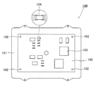
図1に示すように、制御装置(電子コントロールユニット:ECU)100は、主に、本体ケース101と、ビス等の固定手段102によって本体ケース101に固定配置されたプリント基板(基板)105と、を備えている。
As shown in FIG. 1, a control device (electronic control unit: ECU) 100 mainly includes a
前記プリント基板105には、例えば車両に搭載された車載機器等の外部機器を制御するIC103やコンデンサ104等の電子部品がはんだ付け等により適宜の位置に実装されている。なお、プリント基板105は、例えばガラスエポキシ樹脂等の絶縁樹脂等から形成され、その表面には適宜の配線回路パターン(不図示)が形成され、前記電子部品とその配線回路パターンとによって外部機器を制御する制御回路が構成されている。
On the printed
前記本体ケース101の下面には、図2に示すように、略矩形状の貫通孔106が形成され、この貫通孔106にコネクタ110が嵌合され、コネクタ110を介してプリント基板105と外部機器や外部配線とが電気的に接続されるようになっている。
As shown in FIG. 2, a substantially rectangular through
コネクタ110は、図3に示すように、主に、プリント基板105と外部機器や外部配線とを接続するための複数の接続端子111と、この複数の接続端子111を収容して保護するためのコネクタハウジング112と、例えば車両に搭載されたモータやインジェクタ(燃料噴射弁)などのアクチュエータの動作や配線への通電に起因するノイズや静電気を遮断もしくは低減するための積層セラミックコンデンサ(積層コンデンサ)113と、を有している。
As shown in FIG. 3, the
前記接続端子111は棒状を呈しており、後述するように、例えば100本以上の入出力ピン111aとグランドピン111bとを有している(図6参照)。
The
コネクタハウジング112は、主に、断面が略矩形状であって本体ケース101の貫通孔106と相補的な形状を有し且つ複数の接続端子111の周囲を覆う筒体114と、該筒体114のプリント基板105側の端部を閉塞する底板115と、を有している。
The
前記筒体114の外周面には、本体ケース101の貫通孔106に嵌合された際に本体ケース101に対するコネクタハウジング112の位置を規定する突部116が形成されている。また、底板115には、図4に示すように、接続端子111の一部を通すための貫通孔117が形成されると共に、その略中心には積層セラミックコンデンサ113を位置決めするための位置決め部118が形成されている。また、筒体114のプリント基板105側の端部と底板115とで形成される角部には、筒体114の形状を保持するための厚肉部119が形成されており、底板115と厚肉部119とで画成される領域に積層セラミックコンデンサ113が配置されている。
On the outer peripheral surface of the
ここで、積層セラミックコンデンサ113の周囲と厚肉部119との間には、図5に示すように、例えばシリコン等から形成される弾性を有する樹脂粘着材(緩衝材)120が取り付けられており、樹脂粘着材120で挟持され且つ底板115に当接した姿勢で積層セラミックコンデンサ113がコネクタハウジング112に一体的に固定配置されている。これにより、例えば当該制御装置100が車両に搭載され、車両走行等によって制御装置100に振動が発生する場合であっても、その振動に起因する積層セラミックコンデンサ113に対する衝撃を緩和することができる。なお、積層セラミックコンデンサ113に対する衝撃が小さい場合には、積層セラミックコンデンサ113の周囲に配設された樹脂粘着材120を省略することができる。
Here, between the periphery of the multilayer
積層セラミックコンデンサ113には、コネクタハウジング112の底板115に形成された貫通孔117や位置決め部118に対応する位置に、接続端子111を通すための貫通孔121や位置決め部118を通すための位置決め孔122が形成されている。
The multilayer
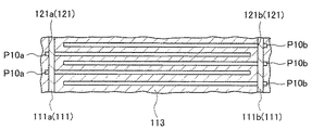
図6は、図4に示す積層セラミックコンデンサの一部を拡大して示したものである。また、図7Aは、図6に示す積層セラミックコンデンサを形成する端子用誘電体シートを示したものであり、図7Bは、そのグランド用誘電体シートを示したものである。 FIG. 6 is an enlarged view of a part of the multilayer ceramic capacitor shown in FIG. FIG. 7A shows a dielectric sheet for terminals that forms the multilayer ceramic capacitor shown in FIG. 6, and FIG. 7B shows the dielectric sheet for ground.
図6に示すように、積層セラミックコンデンサ113は、端子用回路パターンP10aが印刷された端子用誘電体シートとグランド用回路パターンP10bが印刷されたグランド用誘電体シートとが交互に積層されて一体とされて形成されている。上記するように、積層セラミックコンデンサ113には、接続端子111を通すための貫通孔121が積層方向へ向かって形成されており、接続端子111のうち入出力ピン111aが貫通孔121のうち端子用の貫通孔121aに積層方向へ向かって嵌挿されて端子用回路パターンP10aと電気的に接続され、接続端子111のうちグランドピン111bが貫通孔121のうちグランド用の貫通孔121bに積層方向へ向かって嵌挿されてグランド用回路パターンP10bと電気的に接続されている。
As shown in FIG. 6, in the multilayer
より具体的には、図7A及び図7Bに示すように、積層セラミックコンデンサ113は、接続端子111のうち入出力ピン111aと電気的に接続される端子接続パターンP12a及び端子接続パターンP12aに連接する端子側電極パターンP11aからなる端子用回路パターンP10aが印刷された端子用誘電体シート123aと、端子側電極パターンP11aと対向配置(積層方向で視た際に端子側電極パターンP11aと重なるように配置)されるグランド側電極パターンP11b及びグランド側電極パターンP11bに連接するグランドパターンP12bからなるグランド用回路パターンP10bが印刷されたグランド用誘電体シート123bと、が交互に積層されて形成されている。
More specifically, as shown in FIGS. 7A and 7B, the multilayer
そして、複数の入出力ピン111aが端子用回路パターンP10aの端子接続パターンP12aのそれぞれに形成された貫通孔121aa(121a)に積層方向へ向かって嵌挿され、入出力ピン111aと端子用回路パターンP10aとが電気的に接続されている。なお、グランド用誘電体シート123bには、端子接続パターンP12aに対応する位置に入出力ピン111aを通すための貫通孔121ab(121a)が積層方向へ向かってそれぞれ形成されており、入出力ピン111aとグランド用回路パターンP10bとが導通しないようになっている。
A plurality of input /
また、グランドピン111bがグランド用回路パターンP10bのグランドパターンP12b、特にグランドパターンP12bのグランド部P12cに形成された貫通孔121bb(121b)に積層方向へ向かって嵌挿され、グランドピン111bとグランド用回路パターンP10bとが電気的に接続されている。なお、端子用誘電体シート123aには、グランドパターンP12bのグランド部P12cに対応する位置にグランドピン111bを通すための貫通孔121ba(121b)が積層方向へ向かって形成され、グランドピン111bと端子用回路パターンP10aとが導通しないようになっている。
In addition, the
図8及び図9を参照して、図6に示す積層セラミックコンデンサを製造する工程を概説する。 With reference to FIG. 8 and FIG. 9, the process of manufacturing the multilayer ceramic capacitor shown in FIG. 6 will be outlined.
積層セラミックコンデンサ113を製造するに当たり、まず、第1工程では、例えばチタン酸バリウム等からなるスラリー状の誘電材料(セラミック材料)をシート状に形成し、例えば厚みが1μm程度の誘電体シート123を作成する(図9のS801)。
In manufacturing the multilayer
次いで、第2工程では、例えば厚膜印刷技術を利用して、例えばニッケルペーストからなる各回路パターン(端子用回路パターンP10a又はグランド用回路パターンP10b)を誘電体シート123に印刷して端子用誘電体シート123aとグランド用誘電体シート123bを作成する(図9のS802)。
Next, in the second step, for example, using a thick film printing technique, each circuit pattern (terminal circuit pattern P10a or ground circuit pattern P10b) made of, for example, nickel paste is printed on the
次に、第3工程では、端子用誘電体シート123aとグランド用誘電体シート123bを適宜の向きで交互に積層(例えばそれぞれ300層ずつ計600層)させて積層体124を作成する(図9のS803)。なお、端子用誘電体シート123aとグランド用誘電体シート123bの積層数は、必要とされるコンデンサ容量に応じて変更することができる。
Next, in a third step, the
次に、第4工程では、プレス機を用いてその積層体124を予め設定された圧力で積層方向へプレスして積層セラミック125を作成する(図9のS804)。
Next, in the fourth step, the laminated ceramic 125 is produced by pressing the
次に、第5工程では、例えばプリント基板に対する層間接触技術を利用したスルーホール加工を積層セラミック125に施し、端子用誘電体シート123aの端子用回路パターンP10aの端子接続パターンP12a及びグランド用誘電体シート123bのグランド用回路パターンP10bのグランドパターンP12bのグランド部P12cに対応する位置に適宜の大きさの貫通孔121a、121bを形成する(図9のS805)。なお、例えばプリント基板等に対する適宜の端面処理技術を用いて、貫通孔121a、121bの端面を処理してもよい。
Next, in the fifth step, for example, through-hole processing using an interlayer contact technique with respect to the printed circuit board is performed on the
そして、第6工程では、裁断機を用いて貫通孔121a、121bが形成された積層セラミック125を例えばコネクタハウジング112の大きさや接続端子111の数量に応じた適宜の大きさに(例えば積層方向で視てコネクタハウジング112の底板115よりも小さい外形となるように)裁断し(図9のS806)、第7工程では、裁断された積層セラミック125を高温雰囲気下で焼成して所望の大きさの積層セラミックコンデンサ113を製造する(図9のS807)。
In the sixth step, the multilayer ceramic 125 in which the through
なお、上記する工程によって製造された積層セラミックコンデンサ113の貫通孔121a、121bに、複数の入出力ピン111aやグランドピン111b等の接続端子111を積層方向(積層セラミックコンデンサ113の表面に対して略垂直方向)へ嵌挿し、積層セラミックコンデンサ113の周囲に樹脂粘着材120を取り付けた状態でコネクタハウジング112の底板115に当接して固定配置することにより、コネクタ110が製造される。
Note that the
このように、本実施の形態1によれば、複数の接続端子111と電気的に接続される端子接続パターンP12a及び端子接続パターンP12aに連接する端子側電極パターンP11aを有する端子用回路パターンP10aが印刷された端子用誘電体シート123aと、端子用回路パターンP10aの端子側電極パターンP11aと対向配置されるグランド側電極パターンP11b及びグランド側電極パターンP11bに連接するグランドパターンP12bを有するグランド用回路パターンP10bが印刷されたグランド用誘電体シート123bとが交互に積層されて一体とされた回路パターン入りの積層セラミックコンデンサ113を採用することにより、端子側電極パターンP11aとグランド側電極パターンP11bを誘電材料を介して配置することができるため、積層セラミックコンデンサ113やこの積層セラミックコンデンサ113が実装されるコネクタ110、そのコネクタ110を用いた制御装置100を大型化することなく、コンデンサ容量を高めることができる。
Thus, according to the first embodiment, the terminal circuit pattern P10a having the terminal connection pattern P12a electrically connected to the plurality of
また、コンデンサ容量を規定する端子用回路パターンP10aの端子側電極パターンP11aやグランド用回路パターンP10bのグランド側電極パターンP11bは、各誘電体シート123に対する印刷により形成されているため、端子用誘電体シート123aやグランド用誘電体シート123bを作製する際に簡便に端子用回路パターンP10aの端子側電極パターンP11aやグランド用回路パターンP10bのグランド側電極パターンP11bを変更して各接続端子(入出力ピン)におけるコンデンサ容量を調整することができる。
Further, since the terminal side electrode pattern P11a of the terminal circuit pattern P10a defining the capacitor capacity and the ground side electrode pattern P11b of the ground circuit pattern P10b are formed by printing on each
例えば、図10に示すように、端子用誘電体シート123aの端子用回路パターンP10aやグランド用誘電体シート123bのグランド用回路パターンP10bを印刷する際に、端子用回路パターンP10aの端子側電極パターンP11aやグランド用回路パターンP10bのグランド側電極パターンP11bの一部(図中、Ba部及びBb部)を省略したり、それらの印刷面積を低減することにより、簡便にコンデンサ容量を低減することができる。
For example, as shown in FIG. 10, when the terminal circuit pattern P10a of the
また、例えば、図11に示すように、端子用誘電体シート123aの端子用回路パターンP10aやグランド用誘電体シート123bのグランド用回路パターンP10bを印刷する際に、端子用回路パターンP10aの端子側電極パターンP11aやグランド用回路パターンP10bのグランド側電極パターンP11bの一部(図中、Ca部及びCb部)の印刷面積を増加することにより、簡便にコンデンサ容量を増加することができる。
For example, as shown in FIG. 11, when printing the terminal circuit pattern P10a of the
また、本実施の形態1によれば、小型且つ軽量であって高容量を実現し得る積層セラミックコンデンサ113をコネクタハウジング112の内部、特にコネクタハウジング112の底板115に当接して配置し、当該積層セラミックコンデンサ113をコネクタ110に内蔵して一体化することにより、例えばコネクタ110や電子部品が実装されるプリント基板105を小型化することができるため、制御装置100全体を効果的に小型化・軽量化することができる。さらに、積層セラミックコンデンサ113をコネクタ110に一体化した姿勢で当該コネクタ110を制御装置100の本体ケース101に取り付けることができるため、制御装置100の製造工数を削減することができ、その製造コストを抑制できるといった利点もある。
Further, according to the first embodiment, the multilayer
[実施の形態2]
図12は、本発明に係る制御装置の実施の形態2に適用されるコネクタの基本構成を示したものである。本実施の形態2は、実施の形態1に対してコネクタの接続端子の構成が相違しており、その他の構成は実施の形態1と同様である。したがって、実施の形態1と同様の構成については同様の符号を付してその詳細な説明は省略する。
[Embodiment 2]
FIG. 12 shows a basic configuration of a connector applied to Embodiment 2 of the control device according to the present invention. The second embodiment is different from the first embodiment in the configuration of the connection terminals of the connector, and the other configurations are the same as those in the first embodiment. Therefore, the same components as those in the first embodiment are denoted by the same reference numerals, and detailed description thereof is omitted.
図12に示すコネクタ110Aは、プリント基板と外部機器や外部配線とを接続する接続端子111Aが、端子用回路パターンの端子接続パターンやグランド用回路パターンのグランドパターンのグランド部に対応する位置に積層方向へ向かって形成された貫通孔121aA、121bAに充填されて固化された導電材125aA、125bAから形成されている。ここで、前記貫通孔121aA、121bAに充填された導電材125aA、125bAは、積層セラミックコンデンサ113Aの表面と略面一となるように形成されている。
In the
すなわち、本実施の形態2では、端子用回路パターンの端子接続パターンやグランド用回路パターンのグランドパターンのグランド部に対応する位置に積層方向へ向かって形成された貫通孔121aA、121bAに例えばはんだ等からなる溶融状態の導電材を充填し、該導電材を所定の雰囲気下で固化させることによって、その表面が積層セラミックコンデンサ113Aの表面と略面一となる導電材125aAからなる入出力端子111aA及び導電材125bAからなるグランド端子111bAといった接続端子111Aが形成されている。
That is, in the second embodiment, the through holes 121aA and 121bA formed in the direction corresponding to the ground portion of the terminal connection pattern of the terminal circuit pattern and the ground pattern of the ground circuit pattern are soldered, for example. By filling the conductive material in a molten state and solidifying the conductive material in a predetermined atmosphere, an input / output terminal 111aA made of the conductive material 125aA whose surface is substantially flush with the surface of the multilayer
このように、本実施の形態2によれば、貫通孔121aA、121bAに充填された導電材125aA、125bAから入出力端子111aAやグランド端子111bAといった接続端子111Aを形成することによって、例えばUSBコネクタ等に使用される積層セラミックコンデンサ113Aの表面と略面一な表面を有する接続端子を備えたコネクタを簡単に製造することができ、当該コネクタ110Aの適用分野を拡張することができる。
Thus, according to the second embodiment, by forming the connection terminal 111A such as the input / output terminal 111aA and the ground terminal 111bA from the conductive materials 125aA and 125bA filled in the through holes 121aA and 121bA, for example, a USB connector or the like A connector having a connection terminal having a surface substantially flush with the surface of the multilayer
なお、図12に示す雄側のコネクタ110Aに対応する雌側のコネクタMは、図13に示すように、セラミック等からなる誘電体に対してコネクタ110Aの貫通孔121aA、121bAに対応する位置に貫通孔MaA、MbAを形成し、該貫通孔MaA、MbAに接続端子を形成する導電材を充填して固化させる、もしくは、該貫通孔MaA、MbAに接続端子を形成する接続用の金属ピンを嵌挿入することによって製造することができる。
The female connector M corresponding to the
[実施の形態3]
図14は、本発明に係る制御装置の実施の形態3に適用されるコネクタの基本構成を示したものである。本実施の形態3は、実施の形態1、2に対してコネクタの接続端子や表面に印刷される回路パターンの構成が相違しており、その他の構成は実施の形態1、2と同様である。したがって、実施の形態1、2と同様の構成についてはその詳細な説明は省略する。
[Embodiment 3]
FIG. 14 shows a basic configuration of a connector applied to the third embodiment of the control device according to the present invention. The third embodiment is different from the first and second embodiments in the configuration of the connection terminal of the connector and the circuit pattern printed on the surface, and the other configurations are the same as those in the first and second embodiments. . Therefore, the detailed description of the same configuration as in the first and second embodiments is omitted.
図14に示すコネクタ110Bは、例えばUSBコネクタ等に使用される接触式のコネクタであって、上記する実施の形態2と同様、端子用誘電体シートに印刷された端子用回路パターンの端子接続パターンやグランド用誘電体シートに印刷されたグランド用回路パターンのグランドパターンのグランド部に対応する位置に積層セラミックコンデンサ113Bの積層方向へ向かって形成された貫通孔121aB、121bBに、例えばはんだ等からなる導電材125aB、125bBが充填されて固化され、接続端子111Bを形成する入出力端子111aBやグランド端子111bBの一部が形成されている。
A connector 110B shown in FIG. 14 is a contact-type connector used for a USB connector, for example, and, like the second embodiment described above, a terminal connection pattern of a terminal circuit pattern printed on a terminal dielectric sheet The through holes 121aB and 121bB formed in the direction of the lamination of the multilayer
また、本実施の形態3では、略矩形状のコネクタ110Bの表面の一側縁上に、接続端子111Bの一部を形成する略平板状の複数(図中、19個)の(入出力用)接触端子126aBと(グランド用)接触端子126bBが配置されている。 In the third embodiment, a plurality of substantially flat plate-like (19 in the figure) (input / output) are formed on one side edge of the surface of the substantially rectangular connector 110B. ) Contact terminal 126aB and (for ground) contact terminal 126bB are arranged.
そして、コネクタ110Bの表面の一側縁上に配列された各接触端子126aBと貫通孔121aBに充填された導電材125aBが積層セラミックコンデンサ113Bの表面に追加的に印刷された回路パターン127aBを介して導通されることによって、導電材125aBと回路パターン127aBと接触端子126aBとからなる入出力端子111aBが形成される。
The contact terminals 126aB arranged on one side edge of the surface of the connector 110B and the conductive material 125aB filled in the through holes 121aB are additionally printed on the surface of the multilayer
また、コネクタ110Bの表面の一側縁上に配列された接触端子126bBと貫通孔121bBに充填された導電材125bBが積層セラミックコンデンサ113Bの表面に追加的に印刷された回路パターン127bBを介して導通されることによって、導電材125bBと回路パターン127bBと接触端子126bBとからなるグランド端子111bBが形成される。
Further, the contact terminals 126bB arranged on one side edge of the surface of the connector 110B and the conductive material 125bB filled in the through hole 121bB are electrically connected through the circuit pattern 127bB additionally printed on the surface of the multilayer
すなわち、本実施の形態3では、端子用回路パターンの端子接続パターンが、各貫通孔121aBに充填された導電材125aBと積層セラミックコンデンサ113Bの表面に形成された回路パターン127aBと入出力用の接触端子126aBとからなる入出力端子111aBと電気的に接続され、グランド用回路パターンのグランドパターンが、貫通孔121bBに充填された導電材125bBと積層コンデンサ113Bの表面に形成された回路パターン127bBとグランド用の接触端子126bBとからなるグランド端子111bBと電気的に接続されている。
That is, in the third embodiment, the terminal connection pattern of the terminal circuit pattern is the input / output contact with the conductive material 125aB filled in each through hole 121aB and the circuit pattern 127aB formed on the surface of the multilayer
このように、本実施の形態3によれば、貫通孔121aB、121bBに充填された導電材125aB、125bBと積層コンデンサ113Bの表面に形成された回路パターン127aB、127bBとコネクタ110Bの表面の一側縁上に配列された接触端子126aB、126bBとから入出力端子111aBやグランド端子111bBといった接続端子111Bを形成することによって、例えばUSBコネクタ等に使用される小型且つ軽量であって高容量の接触型コネクタを簡単に製造することができ、当該コネクタ110Bの適用分野を拡張することができる。
As described above, according to the third embodiment, the conductive patterns 125aB and 125bB filled in the through holes 121aB and 121bB, the circuit patterns 127aB and 127bB formed on the surface of the
なお、上記する実施の形態1、2では、コンデンサ容量を確保するために積層セラミックコンデンサを形成する誘電体シートがチタン酸バリウム(BaTiO3)から形成される形態について説明したが、誘電体シートは、例えばチタン酸カルシウム(CaTiO3)やチタン酸ストロンチウム(SrTiO3)、ジルコン酸カルシウム(CaZrO3)等から形成してもよい。 In the first and second embodiments described above, the dielectric sheet for forming the multilayer ceramic capacitor in order to secure the capacitor capacity has been described as being formed from barium titanate (BaTiO 3 ). For example, calcium titanate (CaTiO 3 ), strontium titanate (SrTiO 3 ), calcium zirconate (CaZrO 3 ), or the like may be used.
また、誘電体シートの表面や積層セラミックコンデンサの表面に印刷される回路パターンは、接続端子の基数や配列等の要求される性能に応じて適宜変更することができる。 In addition, the circuit pattern printed on the surface of the dielectric sheet or the surface of the multilayer ceramic capacitor can be appropriately changed according to required performance such as the number and arrangement of the connection terminals.
また、例えば、積層セラミックコンデンサを内蔵するコネクタハウジングの形状や大きさ、本体ケースに対するコネクタの配置位置や固定方法、本体ケースに対するプリント基板の配置位置や固定方法、プリント基板に対する電子部品の配置位置や固定方法、電子部品の種類や基数等は適宜変更することができる。 Also, for example, the shape and size of the connector housing containing the multilayer ceramic capacitor, the position and fixing method of the connector relative to the main body case, the position and fixing method of the printed circuit board relative to the main body case, the position of electronic components relative to the printed circuit board, The fixing method, the type and the number of electronic parts, etc. can be changed as appropriate.
なお、本発明は上記した実施の形態1〜3に限定されるものではなく、様々な変形形態が含まれる。例えば、上記した実施の形態1〜3は本発明を分かりやすく説明するために詳細に説明したものであり、必ずしも説明した全ての構成を備えるものに限定されるものではない。また、ある実施の形態の構成の一部を他の実施の形態の構成に置き換えることが可能であり、また、ある実施の形態の構成に他の実施の形態の構成を加えることも可能である。また、実施の形態1〜3の構成の一部について、他の構成の追加・削除・置換をすることが可能である。 In addition, this invention is not limited to above-described Embodiment 1-3, Various deformation | transformation forms are included. For example, the above-described first to third embodiments are described in detail for easy understanding of the present invention, and are not necessarily limited to those having all the configurations described. Further, a part of the configuration of one embodiment can be replaced with the configuration of another embodiment, and the configuration of another embodiment can be added to the configuration of one embodiment. . Further, it is possible to add, delete, and replace other configurations for a part of the configurations of the first to third embodiments.
また、制御線や情報線は説明上必要と考えられるものを示しており、製品上必ずしも全ての制御線や情報線を示しているとは限らない。実際には殆ど全ての構成が相互に接続されていると考えてもよい。 Further, the control lines and information lines indicate what is considered necessary for the explanation, and not all the control lines and information lines on the product are necessarily shown. Actually, it may be considered that almost all the components are connected to each other.
100 制御装置
101 本体ケース
102 固定手段
103 IC
104 コンデンサ
105 プリント基板(基板)
106 本体ケースの貫通孔
110 コネクタ
111 接続端子
111a 入出力ピン
111b グランドピン
112 コネクタハウジング
113 積層セラミックコンデンサ(積層コンデンサ)
114 コネクタハウジングの筒体
115 コネクタハウジングの底板
116 筒体の突部
117 底板の貫通孔
118 位置決め部
119 厚肉部
120 樹脂粘着材(緩衝材)
121 積層セラミックコンデンサの貫通孔
122 積層セラミックコンデンサの位置決め孔
123 誘電体シート
123a 端子用誘電体シート
123b グランド用誘電体シート
124 端子用誘電体シートとグランド用誘電体シートの積層体
P10a 端子用回路パターン
P10b グランド用回路パターン
P11a 端子側電極パターン
P11b グランド側電極パターン
P12a 端子接続パターン
P12b グランドパターン
100 control unit
101 Body case
102 Fixing means
103 IC
104 capacitors
105 Printed circuit board (board)
106 Body case through-hole
110 connector
111 Connection terminal
111a I / O pin
111b Ground pin
112 Connector housing
113 Multilayer ceramic capacitors (multilayer capacitors)
114 Connector housing cylinder
115 Bottom plate of connector housing
116 Tube protrusion
117 Bottom plate through hole
118 Positioning part
119 Thick part
120 Resin adhesive (buffer material)
121 Multilayer ceramic capacitor through hole
122 Multilayer ceramic capacitor positioning holes
123 dielectric sheet
123a Dielectric sheet for terminals
123b Dielectric sheet for ground
124 Laminate of dielectric sheet for terminals and dielectric sheet for ground
Circuit pattern for P10a terminal
Circuit pattern for P10b ground
P11a Terminal side electrode pattern
P11b Ground side electrode pattern
P12a terminal connection pattern
P12b ground pattern
Claims (17)
前記コネクタは、前記基板と前記外部機器又は外部配線とを接続する複数の接続端子と、端子用回路パターンが印刷された端子用誘電体シートとグランド用回路パターンが印刷されたグランド用誘電体シートとが交互に積層されて一体とされた積層コンデンサと、を有し、
前記端子用回路パターンは、前記複数の接続端子と電気的に接続される端子接続パターン及び該端子接続パターンに連接する端子側電極パターンを有し、前記グランド用回路パターンは、前記端子側電極パターンと対向配置されるグランド側電極パターン及び該グランド側電極パターンに連接するグランドパターンを有し、
前記端子用回路パターンの端子接続パターン及び/又は前記グランド用回路パターンのグランドパターンに対応する位置には前記積層コンデンサの積層方向へ向かって貫通孔が形成され、該貫通孔に前記接続端子が配設されて、前記端子用回路パターンの端子接続パターン及び/又は前記グランド用回路パターンのグランドパターンと前記接続端子とが電気的に接続されていることを特徴とする制御装置。 A control device comprising a board on which an electronic component for controlling an external device is mounted, and a connector for electrically connecting the board and the external device or external wiring,
The connector includes a plurality of connection terminals for connecting the substrate and the external device or external wiring, a terminal dielectric sheet printed with a terminal circuit pattern, and a ground dielectric sheet printed with a ground circuit pattern. And a multilayer capacitor that is alternately laminated and integrated,
The terminal circuit pattern includes a terminal connection pattern electrically connected to the plurality of connection terminals and a terminal side electrode pattern connected to the terminal connection pattern, and the ground circuit pattern includes the terminal side electrode pattern. A ground-side electrode pattern disposed opposite to the ground-side electrode pattern and a ground pattern connected to the ground-side electrode pattern ,
A through hole is formed in a direction corresponding to the terminal pattern of the terminal circuit pattern and / or the ground pattern of the ground circuit pattern in the stacking direction of the multilayer capacitor, and the connection terminal is arranged in the through hole. And a terminal connection pattern of the terminal circuit pattern and / or a ground pattern of the circuit pattern for ground and the connection terminal are electrically connected .
該コネクタは、前記基板と前記外部機器又は外部配線とを接続する複数の接続端子と、端子用回路パターンが印刷された端子用誘電体シートとグランド用回路パターンが印刷されたグランド用誘電体シートとが交互に積層されて一体とされた積層コンデンサと、を有し、
前記端子用回路パターンは、前記複数の接続端子と電気的に接続される端子接続パターン及び該端子接続パターンに連接する端子側電極パターンを有し、前記グランド用回路パターンは、前記端子側電極パターンと対向配置されるグランド側電極パターン及び該グランド側電極パターンに連接するグランドパターンを有し、
前記端子用回路パターンの端子接続パターン及び/又は前記グランド用回路パターンのグランドパターンに対応する位置には前記積層コンデンサの積層方向へ向かって貫通孔が形成され、該貫通孔に前記接続端子が配設されて、前記端子用回路パターンの端子接続パターン及び/又は前記グランド用回路パターンのグランドパターンと前記接続端子とが電気的に接続されていることを特徴とするコネクタ。 A connector for electrically connecting a substrate on which an electronic component for controlling an external device is mounted and the external device or external wiring,
The connector includes a plurality of connection terminals for connecting the substrate and the external device or external wiring, a terminal dielectric sheet printed with a terminal circuit pattern, and a ground dielectric sheet printed with a ground circuit pattern. And a multilayer capacitor that is alternately laminated and integrated,
The terminal circuit pattern includes a terminal connection pattern electrically connected to the plurality of connection terminals and a terminal side electrode pattern connected to the terminal connection pattern, and the ground circuit pattern includes the terminal side electrode pattern. A ground-side electrode pattern disposed opposite to the ground-side electrode pattern and a ground pattern connected to the ground-side electrode pattern ,
A through hole is formed in a direction corresponding to the terminal pattern of the terminal circuit pattern and / or the ground pattern of the ground circuit pattern in the stacking direction of the multilayer capacitor, and the connection terminal is arranged in the through hole. A connector, wherein the terminal connection pattern of the terminal circuit pattern and / or the ground pattern of the ground circuit pattern and the connection terminal are electrically connected .
前記基板と前記外部機器又は外部配線とを接続する複数の接続端子と電気的に接続される端子接続パターン及び該端子接続パターンに連接する端子側電極パターンを有する端子用回路パターンが印刷された端子用誘電体シートと、前記端子側電極パターンと対向配置されるグランド側電極パターン及び該グランド側電極パターンに連接するグランドパターンを有するグランド用回路パターンが印刷されたグランド用誘電体シートとが交互に積層されて一体とされ、
前記端子用回路パターンの端子接続パターン及び/又は前記グランド用回路パターンのグランドパターンに対応する位置に前記積層コンデンサの積層方向へ向かって貫通孔が形成されていることを特徴とするコネクタ用積層コンデンサ。 A multilayer capacitor for a connector for electrically connecting a substrate on which an electronic component for controlling an external device is mounted and the external device or external wiring,
A terminal printed with a terminal connection pattern electrically connected to a plurality of connection terminals connecting the substrate and the external device or external wiring, and a terminal circuit pattern connected to the terminal connection pattern. The dielectric sheet for ground and the dielectric sheet for ground on which the ground circuit pattern having the ground pattern connected to the ground electrode pattern and the ground pattern connected to the ground electrode pattern are printed alternately Laminated and united ,
A multilayer capacitor for a connector, characterized in that a through hole is formed in a direction corresponding to the terminal pattern of the terminal circuit pattern and / or the ground pattern of the circuit pattern for ground in the multilayer direction of the multilayer capacitor. .
Priority Applications (5)
| Application Number | Priority Date | Filing Date | Title |
|---|---|---|---|
| JP2013108172A JP6129643B2 (en) | 2013-05-22 | 2013-05-22 | Control device, connector, and multilayer capacitor for connector |
| CN201480028626.1A CN105228863B (en) | 2013-05-22 | 2014-03-10 | Control apparatus, connector, and laminated capacitor for connector |
| EP14801888.0A EP3000664B1 (en) | 2013-05-22 | 2014-03-10 | Control apparatus, connector, and laminated capacitor for connector |
| PCT/JP2014/056100 WO2014188758A1 (en) | 2013-05-22 | 2014-03-10 | Control apparatus, connector, and laminated capacitor for connector |
| US14/787,338 US9705261B2 (en) | 2013-05-22 | 2014-03-10 | Control apparatus, connector, and laminated capacitor for connector |
Applications Claiming Priority (1)
| Application Number | Priority Date | Filing Date | Title |
|---|---|---|---|
| JP2013108172A JP6129643B2 (en) | 2013-05-22 | 2013-05-22 | Control device, connector, and multilayer capacitor for connector |
Publications (2)
| Publication Number | Publication Date |
|---|---|
| JP2014227039A JP2014227039A (en) | 2014-12-08 |
| JP6129643B2 true JP6129643B2 (en) | 2017-05-17 |
Family
ID=51933324
Family Applications (1)
| Application Number | Title | Priority Date | Filing Date |
|---|---|---|---|
| JP2013108172A Active JP6129643B2 (en) | 2013-05-22 | 2013-05-22 | Control device, connector, and multilayer capacitor for connector |
Country Status (5)
| Country | Link |
|---|---|
| US (1) | US9705261B2 (en) |
| EP (1) | EP3000664B1 (en) |
| JP (1) | JP6129643B2 (en) |
| CN (1) | CN105228863B (en) |
| WO (1) | WO2014188758A1 (en) |
Cited By (1)
| Publication number | Priority date | Publication date | Assignee | Title |
|---|---|---|---|---|
| JP7187027B2 (en) | 2019-02-18 | 2022-12-12 | スターテング工業株式会社 | seat armrest structure |
Families Citing this family (4)
| Publication number | Priority date | Publication date | Assignee | Title |
|---|---|---|---|---|
| JP6129643B2 (en) * | 2013-05-22 | 2017-05-17 | 日立オートモティブシステムズ株式会社 | Control device, connector, and multilayer capacitor for connector |
| US9680261B2 (en) * | 2014-06-11 | 2017-06-13 | Honewell International Inc. | Intrinsic safe in-line adaptor with integrated capacitive barrier for connecting a wireless module with antenna |
| KR101792381B1 (en) * | 2016-01-04 | 2017-11-01 | 삼성전기주식회사 | Electronic component and manufaturing method for the same |
| US11967788B2 (en) * | 2022-04-22 | 2024-04-23 | Rheem Manufacturing Company | Plug-in connector with authentication feature |
Family Cites Families (20)
| Publication number | Priority date | Publication date | Assignee | Title |
|---|---|---|---|---|
| JPH05234643A (en) | 1992-02-21 | 1993-09-10 | Tdk Corp | Counter-noise type connector and noise removing parts for counter-noise type connector |
| US5580279A (en) * | 1994-10-31 | 1996-12-03 | Berg Technology, Inc. | Low cost filtered and shielded electronic connector and method of use |
| US5905627A (en) * | 1997-09-10 | 1999-05-18 | Maxwell Energy Products, Inc. | Internally grounded feedthrough filter capacitor |
| US6165018A (en) * | 1999-04-27 | 2000-12-26 | Lucent Technologies Inc. | Connector having internal crosstalk compensation |
| JP2001307910A (en) * | 2000-04-25 | 2001-11-02 | Tdk Corp | Laminated electronic parts array |
| US6882248B2 (en) * | 2000-09-07 | 2005-04-19 | Greatbatch-Sierra, Inc. | EMI filtered connectors using internally grounded feedthrough capacitors |
| DE10233318C1 (en) * | 2002-07-22 | 2003-09-25 | Siemens Ag | Interference suppression device for electronic apparatus uses capacitor connected between plug element for apparatus circuit and housing potential |
| JP2005310531A (en) * | 2004-04-21 | 2005-11-04 | Auto Network Gijutsu Kenkyusho:Kk | Electric equipment |
| JP4960583B2 (en) * | 2004-07-07 | 2012-06-27 | Tdk株式会社 | Laminated LC composite parts |
| KR100678083B1 (en) * | 2004-11-11 | 2007-02-02 | 삼성전자주식회사 | Fabricating method of the embedded capacitor and embedded capacitor using the same |
| EP1760735B1 (en) * | 2005-09-02 | 2015-03-11 | Greatbatch Ltd. | Screen-printed capacitors for filter feedthrough assemblies |
| US7564674B2 (en) * | 2005-12-12 | 2009-07-21 | Greatbatch Ltd. | Feedthrough filter capacitor assemblies having low cost terminal pins |
| JP4851243B2 (en) | 2006-03-20 | 2012-01-11 | 株式会社オートネットワーク技術研究所 | Joint connector with built-in capacitor |
| WO2009119875A1 (en) * | 2008-03-24 | 2009-10-01 | 日本特殊陶業株式会社 | Component-incorporating wiring board |
| JP5174071B2 (en) | 2010-03-16 | 2013-04-03 | 日立オートモティブシステムズ株式会社 | Electronic equipment |
| CN102196703B (en) | 2010-03-16 | 2015-10-14 | 日立汽车系统株式会社 | Electronic equipment |
| EP2398026B1 (en) * | 2010-06-15 | 2019-08-21 | Greatbatch Ltd. | Coating of non-solderable base metal for soldering application in medical device component |
| US8642887B1 (en) * | 2010-12-03 | 2014-02-04 | Greatbatch Ltd. | Metallization barrier for a hermetic feedthrough |
| EP2529790B1 (en) * | 2011-06-03 | 2017-09-20 | Greatbatch Ltd. | Feedthrough wire connector for use in a medical device |
| JP6129643B2 (en) * | 2013-05-22 | 2017-05-17 | 日立オートモティブシステムズ株式会社 | Control device, connector, and multilayer capacitor for connector |
-
2013
- 2013-05-22 JP JP2013108172A patent/JP6129643B2/en active Active
-
2014
- 2014-03-10 WO PCT/JP2014/056100 patent/WO2014188758A1/en active Application Filing
- 2014-03-10 EP EP14801888.0A patent/EP3000664B1/en active Active
- 2014-03-10 CN CN201480028626.1A patent/CN105228863B/en active Active
- 2014-03-10 US US14/787,338 patent/US9705261B2/en active Active
Cited By (1)
| Publication number | Priority date | Publication date | Assignee | Title |
|---|---|---|---|---|
| JP7187027B2 (en) | 2019-02-18 | 2022-12-12 | スターテング工業株式会社 | seat armrest structure |
Also Published As
| Publication number | Publication date |
|---|---|
| US20160072228A1 (en) | 2016-03-10 |
| CN105228863A (en) | 2016-01-06 |
| EP3000664A4 (en) | 2018-03-28 |
| EP3000664B1 (en) | 2020-09-23 |
| WO2014188758A1 (en) | 2014-11-27 |
| CN105228863B (en) | 2017-05-10 |
| EP3000664A1 (en) | 2016-03-30 |
| JP2014227039A (en) | 2014-12-08 |
| US9705261B2 (en) | 2017-07-11 |
Similar Documents
| Publication | Publication Date | Title |
|---|---|---|
| JP6129643B2 (en) | Control device, connector, and multilayer capacitor for connector | |
| JP6552050B2 (en) | Multilayer ceramic electronic components | |
| US9648746B2 (en) | Composite electronic component and board having the same | |
| US10622146B2 (en) | Multilayer capacitor and electronic component device | |
| CN103578743A (en) | Capacitor component and capacitor component mounting structure | |
| US7589953B2 (en) | Multilayer capacitor | |
| US20130134835A1 (en) | Ultrasonic sensor and manufacturing method thereof | |
| JPH08124795A (en) | Multilayered capacitor | |
| JP7058938B2 (en) | Capacitor element mounting structure | |
| KR102620522B1 (en) | Electronic component and board having the same mounted thereon | |
| WO2016067746A1 (en) | Laminated capacitor and in-vehicle control device | |
| JP2016092289A (en) | Mounting structure of capacitor element | |
| JP2014183173A (en) | Circuit board and mounting method for capacitor element | |
| US11302483B2 (en) | Electronic component | |
| JP7003496B2 (en) | Electronic component equipment | |
| JP7003495B2 (en) | Multilayer capacitor | |
| US10943739B2 (en) | Electronic component | |
| EP3454352B1 (en) | Multilayer ceramic capacitor | |
| JP6958429B2 (en) | Multilayer capacitor | |
| JP6930114B2 (en) | Electronic component equipment | |
| KR20210075672A (en) | Electronic component | |
| JP2604203Y2 (en) | Ceramic capacitors | |
| JP3368650B2 (en) | Multilayer ceramic parts | |
| KR20190121221A (en) | Electronic component | |
| JP2018113316A (en) | Composite electronic component |
Legal Events
| Date | Code | Title | Description |
|---|---|---|---|
| A621 | Written request for application examination |
Free format text: JAPANESE INTERMEDIATE CODE: A621 Effective date: 20160204 |
|
| A131 | Notification of reasons for refusal |
Free format text: JAPANESE INTERMEDIATE CODE: A131 Effective date: 20161122 |
|
| A521 | Request for written amendment filed |
Free format text: JAPANESE INTERMEDIATE CODE: A523 Effective date: 20161212 |
|
| TRDD | Decision of grant or rejection written | ||
| A01 | Written decision to grant a patent or to grant a registration (utility model) |
Free format text: JAPANESE INTERMEDIATE CODE: A01 Effective date: 20170404 |
|
| A61 | First payment of annual fees (during grant procedure) |
Free format text: JAPANESE INTERMEDIATE CODE: A61 Effective date: 20170412 |
|
| R150 | Certificate of patent or registration of utility model |
Ref document number: 6129643 Country of ref document: JP Free format text: JAPANESE INTERMEDIATE CODE: R150 |
|
| S533 | Written request for registration of change of name |
Free format text: JAPANESE INTERMEDIATE CODE: R313533 |
|
| R350 | Written notification of registration of transfer |
Free format text: JAPANESE INTERMEDIATE CODE: R350 |
|
| R250 | Receipt of annual fees |
Free format text: JAPANESE INTERMEDIATE CODE: R250 |