JP6097551B2 - Method for manufacturing liquid crystal display device and alignment film printing apparatus - Google Patents
Method for manufacturing liquid crystal display device and alignment film printing apparatus Download PDFInfo
- Publication number
- JP6097551B2 JP6097551B2 JP2012276434A JP2012276434A JP6097551B2 JP 6097551 B2 JP6097551 B2 JP 6097551B2 JP 2012276434 A JP2012276434 A JP 2012276434A JP 2012276434 A JP2012276434 A JP 2012276434A JP 6097551 B2 JP6097551 B2 JP 6097551B2
- Authority
- JP
- Japan
- Prior art keywords
- substrate
- alignment film
- printing
- liquid crystal
- counter
- Prior art date
- Legal status (The legal status is an assumption and is not a legal conclusion. Google has not performed a legal analysis and makes no representation as to the accuracy of the status listed.)
- Active
Links
- 238000007639 printing Methods 0.000 title claims description 128
- 239000004973 liquid crystal related substance Substances 0.000 title claims description 44
- 238000004519 manufacturing process Methods 0.000 title claims description 15
- 238000000034 method Methods 0.000 title description 6
- 239000000758 substrate Substances 0.000 claims description 172
- 239000000463 material Substances 0.000 claims description 10
- 239000010408 film Substances 0.000 description 90
- 239000011248 coating agent Substances 0.000 description 15
- 238000000576 coating method Methods 0.000 description 15
- 241001125929 Trisopterus luscus Species 0.000 description 11
- 230000007423 decrease Effects 0.000 description 6
- 239000007888 film coating Substances 0.000 description 5
- 238000009501 film coating Methods 0.000 description 5
- 239000006185 dispersion Substances 0.000 description 4
- 239000003566 sealing material Substances 0.000 description 4
- 239000007788 liquid Substances 0.000 description 3
- 230000006866 deterioration Effects 0.000 description 2
- 238000010586 diagram Methods 0.000 description 2
- 238000002347 injection Methods 0.000 description 2
- 239000007924 injection Substances 0.000 description 2
- 239000004925 Acrylic resin Substances 0.000 description 1
- 229920000178 Acrylic resin Polymers 0.000 description 1
- 239000000853 adhesive Substances 0.000 description 1
- 230000001070 adhesive effect Effects 0.000 description 1
- 230000002411 adverse Effects 0.000 description 1
- 230000015556 catabolic process Effects 0.000 description 1
- 230000002950 deficient Effects 0.000 description 1
- 238000006731 degradation reaction Methods 0.000 description 1
- 230000005684 electric field Effects 0.000 description 1
- 239000011159 matrix material Substances 0.000 description 1
- 238000007645 offset printing Methods 0.000 description 1
- 239000011368 organic material Substances 0.000 description 1
- 239000010409 thin film Substances 0.000 description 1
- 238000002834 transmittance Methods 0.000 description 1
Images


Landscapes
- Liquid Crystal (AREA)
Description
本発明は液晶表示装置に係り、特に、狭額縁の液晶表示装置における配向膜の印刷方法および配向膜の印刷装置に関する。 The present invention relates to a liquid crystal display device, and more particularly, to an alignment film printing method and an alignment film printing device in a narrow frame liquid crystal display device.
液晶表示装置に使用される液晶表示パネルは、画素電極および薄膜トランジスタ(TFT)等を有する画素がマトリクス状に形成されたTFT基板と、TFT基板に対向して、TFT基板の画素電極と対応する場所にカラーフィルタ等が形成された対向基板が配置され、TFT基板と対向基板の間に液晶が挟持されている。そして液晶分子による光の透過率を画素毎に制御することによって画像を形成している。 A liquid crystal display panel used for a liquid crystal display device includes a TFT substrate in which pixels having pixel electrodes and thin film transistors (TFTs) are formed in a matrix, and a location corresponding to the pixel electrode of the TFT substrate facing the TFT substrate. A counter substrate on which a color filter or the like is formed is disposed, and a liquid crystal is sandwiched between the TFT substrate and the counter substrate. An image is formed by controlling the light transmittance of the liquid crystal molecules for each pixel.
液晶表示装置では、TFT基板と対向基板に形成された配向膜によって、液晶分子の初期配向を行い、この液晶分子の初期配向の状態を、画素電極に映像信号を印加することにより、画素電極と対向電極との間に形成された電界によって変化させることによって、液晶表示パネルを透過する光の量をコントロールしている。液晶分子の初期配向の向きは配向膜をラビング処理あるいは光配向処理することによって規定している。 In a liquid crystal display device, initial alignment of liquid crystal molecules is performed by alignment films formed on a TFT substrate and a counter substrate, and the initial alignment state of the liquid crystal molecules is applied to the pixel electrode by applying a video signal to the pixel electrode. The amount of light passing through the liquid crystal display panel is controlled by changing the electric field formed between the counter electrode and the counter electrode. The direction of the initial alignment of the liquid crystal molecules is defined by rubbing or photoaligning the alignment film.
配向膜は、所定の粘度の液体の有機材料を例えば、オフセット印刷(フレキソ印刷)によってTFT基板あるいは対向基板に塗布し、その後、配向膜材料を焼成してイミド化し、配向膜としている。配向膜のフレキソ印刷は、次のようにして行われる。すなわち、注入ノズルから配向膜材料を円筒状のアニックスロールに滴下し、配向膜材料を液展開手段(ドクターブレード)を用いてアニックスロールに均一に塗布し、これを版胴に巻きつけられた印刷版に転写し、印刷版からTFT基板あるいは対向基板に印刷する。 For the alignment film, a liquid organic material having a predetermined viscosity is applied to the TFT substrate or the counter substrate by, for example, offset printing (flexographic printing), and then the alignment film material is baked and imidized to form an alignment film. Flexographic printing of the alignment film is performed as follows. That is, the alignment film material is dropped onto the cylindrical anix roll from the injection nozzle, the alignment film material is uniformly applied to the anix roll using a liquid developing means (doctor blade), and this is wound around the plate cylinder. It is transferred to a plate and printed on the TFT substrate or counter substrate from the printing plate.
「特許文献1」には、フレキソ印刷した配向膜の膜厚が周辺において厚くなるのと防止するために、印刷版の凸版部の端部をテーパ加工した構成が記載されている。「特許文献2」には、基板における印刷された配向膜の位置を正確に決めるために、基板に形成した位置決めマークと印刷版に形成した位置合わせマークを利用して配向膜の位置ずれを軽減する構成が記載されている。
“
図5は、配向膜のフレキソ印刷の構成を示す模式図である。図5において、図示しない注入ノズルから配向膜材料がアニックスロール15に滴下される。アニックスロール15は矢印の方向に回転するが、このとき、図示しないドクターブレードを揺動することによって、配向膜材料をアニックスロールの軸方向に均一に分布させる。
FIG. 5 is a schematic diagram showing the configuration of flexographic printing of the alignment film. In FIG. 5, the alignment film material is dropped onto the
アニックスロール15に塗布された配向膜材料は、アニックスロール15および版胴16が各々矢印の方向に回転することによって、版胴16の周りに貼り付けられた印刷版39に転写される。一方、TFT基板あるいは対向基板が複数形成されたマザー基板40が図5の矢印の方向に進行し、印刷版30と接触することによってマザー基板40に配向膜140が転写される。
The alignment film material applied to the
印刷版30がマザー基板40と離れる側を印刷入側Pin、印刷版30がマザー基板40と最後に接触する側を印刷出側Poutと定義する。印刷版30は弾性を有するアクリル樹脂で形成されているので、印刷版30とマザー基板40が印刷のために接触すると、印刷版30が版胴16の回転方向と逆側に伸びてくる。この印刷版30の伸びは、印刷入側Pinでは小さいが、印刷出側Poutで大きくなる。このような印刷版30の伸びは制御が困難である。したがって、印刷出側Pout側では、塗布寸法のばらつきが大きくなる。
The side on which the
図6は、マザー基板40に12個の配向膜140が形成された状態を示す平面図である。図6において、配向膜140の各々が1個のTFT基板あるいは1個の対向基板に対応している。すなわち、図6のマザー基板40から12個のTFT基板あるいは対向基板が形成される。
FIG. 6 is a plan view showing a state where 12
図6において、点線で囲った部分が印刷版30の伸びの影響で、配向膜140の寸法のばらつきが最も大きくなる領域である。液晶表示装置の表示領域には必ず配向膜140が存在しなければならず、かりに表示領域の周辺において、配向膜140が存在しなければその液晶表示装置は不良になる。また、配向膜140の寸法が大きすぎて、TFT基板と対向基板を接着するシール材の領域に広く形成されると、シール材の接着力に悪影響を与え、信頼性を低下させることになる。
In FIG. 6, a portion surrounded by a dotted line is a region where the variation in the dimension of the
一方、最近は、液晶表示装置の外形を一定にしたまま、表示領域を大きくとることが要求されている。液晶表示装置の外形を一定にしたまま、表示領域を大きくすると、いわゆる額縁を小さくしなければならない。そうすると、配向膜140の寸法公差を小さくしなければならない。しかし、図6に示すように、印刷出側Poutにおける配向膜寸法のばらつきは避けられないために、配向膜寸法のばらつきに起因する歩留まりの低下、あるいは液晶表示装置のシール部の信頼性の低下が生じていた。
On the other hand, recently, it has been required to increase the display area while keeping the outer shape of the liquid crystal display device constant. If the display area is enlarged while keeping the external shape of the liquid crystal display device constant, the so-called frame must be reduced. Then, the dimensional tolerance of the
本発明の課題は、狭額縁の液晶表示装置において、配向膜の寸法のばらつきが生じても、液晶表示装置の製造歩留まりが低下することを防止し、かつ、液晶表示装置の信頼性の低下を防止した液晶表示装置の製造方法、あるいは、配向膜の塗布装置を実現することである。 An object of the present invention is to prevent a decrease in manufacturing yield of a liquid crystal display device even when a dimensional variation of alignment films occurs in a narrow frame liquid crystal display device, and to reduce the reliability of the liquid crystal display device. An object of the present invention is to realize a liquid crystal display device manufacturing method or an alignment film coating apparatus.
本発明はこのような課題を解決するものであり、具体的な手段は次のとおりである。 The present invention solves such problems, and specific means are as follows.
(1)TFTと画素電極と走査線と映像信号線と配向膜を有するTFT基板と、配向膜を有する対向基板と、前記TFT基板の前記配向膜と前記対向基板の前記配向膜との間に液晶層が挟持された液晶表示装置の製造方法であって、前記TFT基板と前記対向基板が重なった部分に表示領域が形成され、前記TFT基板が1枚になっている部分には端子部が形成され、前記端子部側の前記表示領域の辺と前記対向基板の辺までの距離d2は、前記端子部が形成されていない辺における前記表示領域の辺と前記対向基板の辺までの距離d1よりも大きく、前記TFT基板または前記対向基板の前記配向膜は、印刷版から配向膜材料をTFT基板に転写するフレキソ印刷によって形成され、前記配向膜において、前記印刷版が前記TFT基板または前記対向基板に先に接する側を印刷入側とし、前記印刷版が前記TFT基板または前記対向基板から離れる側を印刷出側とした場合、前記配向膜における前記端子部側の辺は、前記印刷出側側の辺と一致させることを特徴とする液晶表示装置の製造方法である。 (1) A TFT substrate having a TFT, a pixel electrode, a scanning line, a video signal line, an alignment film, a counter substrate having an alignment film, and the alignment film of the TFT substrate and the alignment film of the counter substrate. A method of manufacturing a liquid crystal display device in which a liquid crystal layer is sandwiched, wherein a display region is formed in a portion where the TFT substrate and the counter substrate overlap, and a terminal portion is provided in a portion where the TFT substrate is a single sheet. The distance d2 between the side of the display area formed on the terminal portion side and the side of the counter substrate is a distance d1 between the side of the display area and the side of the counter substrate on the side where the terminal part is not formed. The alignment film of the TFT substrate or the counter substrate is formed by flexographic printing in which an alignment film material is transferred from the printing plate to the TFT substrate. In the alignment film, the printing plate is the TFT substrate or When the side that comes in contact with the counter substrate first is the printing input side, and the printing plate is the side that is away from the TFT substrate or the counter substrate, the side on the terminal portion side of the alignment film is the printing side. It is a manufacturing method of a liquid crystal display device characterized by matching with a side on the exit side.
(2)他の主な手段は、複数のTFT基板または対向基板が形成されたマザー基板の個々のTFT基板または対向基板にフレキソ方式によって配向膜を印刷する配向膜印刷装置であって、前記配向膜印刷装置は、印刷版から前記マザー基板に配向膜を印刷する印刷装置部と、前記印刷装置部の基板投入側に前記マザー基板を、前記マザー基板の長軸を前記印刷装置内の進行方向に対して0°、90°、180°、270°のいずれの向きにおいても、印刷装置に対してセッティング可能な第1の基板旋回部を有し、前記0°、90°、180°、270°のいずれの向きにおいても、位置合わせ可能なアライメント機構を有する基板保持部とアライメントカメラを有し、前記マザー基板に対してフレキソ印刷によって前記配向膜の印刷を行う印刷部と、前記配向膜印刷を終わった前記マザー基板の長軸を前記進行方向に対して0°、90°、180°、270°のいずれの向きに対しても旋回可能な第2の基板旋回部を有することを特徴とする配向膜印刷装置である。 (2) Another main means is an alignment film printing apparatus that prints an alignment film on each TFT substrate or counter substrate of a mother substrate on which a plurality of TFT substrates or counter substrates are formed by a flexo method. The film printing apparatus includes: a printing apparatus unit that prints an alignment film from a printing plate on the mother substrate; the mother substrate on a substrate input side of the printing apparatus unit; and a major axis of the mother substrate in a traveling direction in the printing apparatus The first substrate turning portion that can be set with respect to the printing apparatus in any orientation of 0 °, 90 °, 180 °, and 270 ° with respect to 0 °, 90 °, 180 °, and 270 A printing unit that has a substrate holding unit having an alignment mechanism that can be aligned in any orientation and an alignment camera, and performs printing of the alignment film by flexographic printing on the mother substrate And a second substrate turning portion capable of turning the major axis of the mother substrate after the alignment film printing with respect to any direction of 0 °, 90 °, 180 °, and 270 ° with respect to the traveling direction. An alignment film printing apparatus comprising:
本発明によれば、液晶表示装置において、表示領域の辺と対向基板の辺の間の距離が大きい端子部に対応する配向膜の辺を、フレキソ印刷において塗布ばらつきが大きくなる、印刷版と基板とが離れる側に設定する。したがって、配向膜において、塗布ばらつきが大きい辺が存在しても、このばらつきが液晶表示装置の製造歩留まりを低下させることや製品の信頼性を低下させることを防止することが出来る。 According to the present invention, in the liquid crystal display device, the printing plate and the substrate in which the coating variation is increased in flexographic printing on the side of the alignment film corresponding to the terminal portion having a large distance between the side of the display region and the side of the counter substrate. Set to the side away from. Therefore, even if there is a side having a large coating variation in the alignment film, this variation can prevent the manufacturing yield of the liquid crystal display device from being lowered and the reliability of the product from being lowered.
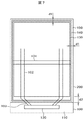
図7は、携帯電話等に使用される液晶表示装置の平面図である。図7において、走査線101、映像信号線102、画素電極、TFT等が形成されたTFT基板100にシール材150を介してカラーフィルタ等が形成された対向基板200が接着している。TFT基板100と対向基板200の間には図示しない液晶層が挟持されている。TFT基板100は対向基板200よりも大きく形成され、TFT基板100が1枚になっている部分には、ICドライバ120等が搭載される端子部110となっている。
FIG. 7 is a plan view of a liquid crystal display device used for a mobile phone or the like. In FIG. 7, a
図7において、端子部110には、映像信号線102および走査線101等からの引出し線103がICドライバ120側に延在している。端子部110の外側端部には図示しないフレキシブル配線基板が接続される。図7におけるTFT基板100と対向基板200が重なった部分に表示領域130が形成されている。表示領域130の全域を覆い、かつ、表示領域130よりもやや大きな面積に配向膜140がフレキソ印刷によって形成されている。
In FIG. 7, a
狭額縁製品の場合、図7における表示領域130の端部から液晶表示装置の外側、すなわち、対向基板200の端部までの距離d1は1mm程度である。ただし、端子部110側の辺においては、表示領域130の端部と対向基板200の端部までの距離d2は1.5mm程度である。端子部110側には、引き出し線103が形成されており、かつ、額縁の幅は液晶表示装置の外形サイズには直接影響しないので、端子部110側の辺においては、表示領域130から対向基板200の端部までの距離が大きくなっている。一方、シール材150の幅は各辺とも同じであるので、端子部110側において表示領域130から対向基板200の端部までの距離が大きい分、配向膜140の塗布ばらつきの公差を大きくすることが出来る。
In the case of a narrow frame product, the distance d1 from the end of the
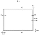
図8は、この様子を示す平面図である。図8は、図7における表示領域130と配向膜塗布領域140の関係を示す平面図である。図8において、配向膜140は、表示領域130よりも若干大きく形成されている。図7で説明したように、端子部110側の辺においては、配向膜140の塗布面積を他の辺よりも大きく形成することが出来る。図8において、表示領域130の端部から配向膜140の端部までの距離は、端子部110側の辺においてs2、他の3辺においてs1であり、s2>s1である。
FIG. 8 is a plan view showing this state. FIG. 8 is a plan view showing the relationship between the
端子部110側の辺では、表示領域130の端部から配向膜140の端部までの距離s2が大きい分、配向膜140の塗布ばらつきの公差Δs2も、他の辺における配向膜140の塗布ばらつきの公差Δs1よりも大きくすることが可能である。本発明は、フレキソ印刷による配向膜140の塗布ばらつきが大きい辺を、液晶表示装置の端子部110側の辺と一致させることによって、液晶表示装置の製造歩留まりの低下を抑え、かつ、シール部の信頼性の低下を抑えている。
In the side on the
図9は印刷版30の展開図である。フレキソ印刷するときは、印刷版30は版胴に巻きつけられている。図9において、印刷版30に配向膜140の印刷パターンが形成されている。この配向膜140の印刷パターンは、点線で示すマザー基板40が矢印の方向に進行するにつれてマザー基板40に転写される。図9のマザー基板40では、横長のマザー基板40に横長の配向膜140が印刷される例である。
FIG. 9 is a development view of the
図9において、右側が、印刷が始まる印刷入側Pinであり、左側が、印刷が終わる印刷出側Poutである。印刷出側Poutでは、印刷版30の伸び等のために、配向膜140の塗布ばらつきが大きくなる。特に図9の点線で示すA領域において、塗布寸法のばらつきが大きい。本発明は、図9におけるA領域の配向膜140の辺を図7における端子部110側の辺と一致させることによって、配向膜140の塗布ばらつきの公差のばらつきが、製造歩留まりの低下、あるいは、製品の信頼性の低下に影響を及ぼすことを防止するものである。
In FIG. 9, the right side is a printing input side Pin where printing starts, and the left side is a printing output side Pout where printing ends. On the printing output side Pout, the coating variation of the
図10は印刷版30の他の例である。図10は、縦長のマザー基板40に横長の配向膜140が印刷される例である。図10は印刷版30の展開図である。フレキソ印刷するときは、印刷版30は版胴に巻きつけられていることは図9の場合と同じである。図10において、印刷版30に配向膜140の印刷パターンが形成されている。この配向膜140の印刷パターンは、点線で示すマザー基板40が矢印の方向に進行するにつれてマザー基板40に転写される。
FIG. 10 shows another example of the
図10において、右側が、印刷が始まる印刷入側Pinであり、左側が、印刷が終わる印刷出側Poutである。印刷出側Poutでは、印刷版30の伸び等のために、配向膜140の塗布ばらつきが大きくなる。特に図10の点線で示すA領域において、塗布寸法のばらつきが大きい。図9で説明したのと同様、本発明では、図10におけるA領域の配向膜140の辺を図7における端子部110側の辺と一致させることによって、配向膜140の塗布ばらつきが、製造歩留まりの低下、あるいは、製品の信頼性の低下に影響を及ぼすことを防止することが出来る。
In FIG. 10, the right side is a printing input side Pin where printing starts, and the left side is a printing output side Pout where printing ends. On the printing output side Pout, the coating variation of the
図9と図10を比較するとわかるように、本発明では、長方形の配向膜140の印刷パターンの向きによって、フレキソ印刷するときのマザー基板40の向きを変化させる。すなわち、液晶表示装置における端子部側の辺をフレキソ印刷における印刷出側Poutの辺、すなわち、図9および図10のA領域と一致させるようにしている。
As can be seen by comparing FIG. 9 and FIG. 10, in the present invention, the orientation of the
以下の実施例では、以上説明したような本発明にかかる液晶表示装置の製造方法を可能にする製造装置について説明する。 In the following embodiments, a manufacturing apparatus that enables the method for manufacturing a liquid crystal display device according to the present invention as described above will be described.
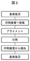
図1は、本発明における配向膜印刷装置の斜視図である。図2は、図1の配向膜印刷装置におけるフローを示す図である。図1に示す本発明の配向膜印刷装置が従来の配向膜印刷装置と異なる第1の特徴は、印刷装置10の前後に基板旋回部20を有していることである。この基板旋回部20において、長方形のマザー基板40の長軸に対して、0°、90°、180°、270°のいずれの向きにおいても、印刷装置10に対してセッティング可能としている。
FIG. 1 is a perspective view of an alignment film printing apparatus according to the present invention. FIG. 2 is a diagram showing a flow in the alignment film printing apparatus of FIG. The first feature that the alignment film printing apparatus of the present invention shown in FIG. 1 is different from the conventional alignment film printing apparatus is that the
マザー基板40はまず、基板旋回部20に投入され、基板旋回部20の動作によって、図7〜図10の説明において述べたように、印刷出側Poutの配向膜140の辺を図7に示す液晶表示装置の端子部110側の辺に一致させる。これが図2における「基板旋回」である。図1の基板旋回部20において、マザー基板40が基板旋回によって、マザー基板40の長軸が基板の進行方向と一致する場合と、基板の進行方向と直角の方向になる場合とが記載されている。
First, the
マザー基板40が基板旋回部20において、所定の向きにセットされた後、印刷装置10の基板保持台11にセッティングされる。これが図2の「印刷装置へ搭載」である。図1に示すように、基板保持台11にはアライメントピン等のアライメント機構12が存在している。印刷装置10に付属のアライメントカメラ14によって、目合わせマーク等を用いて、基板保持台11に対してマザー基板40を所定の位置にセッティングする。これが図2のアライメントである。
After the
図3の左側はこのアライメントの状態を示す平面図である。図3は、マザー基板40の長軸方向が基板の進行方向と一致する場合であり、図3には0°/180°と記載されている。図3において、マザー基板40がハーフトーンの丸で示すいアライメントピン等のアライメント機構12によって、所定の位置にセッティングされている状態を示している。
The left side of FIG. 3 is a plan view showing this alignment state. FIG. 3 shows a case where the major axis direction of the
アライメント機構12によって、マザー基板40を所定の位置にセッティングするために、ハーフトーンの四角で示すアライメントカメラ14によって、マザー基板40および基板保持台11の目合わせマーク等を読み取り、位置制御機構にアライメント制御情報を取得する。なお、図3における白抜きの丸あるいは四角は、マザー基板40が短軸方向に移動する場合に使用するアライメント機構12あるいはアライメントカメラ14の位置であり、マザー基板40が図3のような方向に移動する場合は、アライメント機構12等は、基板保持台11内に収容されている。
In order to set the
基板保持台11において、位置決めされたマザー基板40は図1に示す印刷部に移動して、配向膜印刷される。図1において、版胴16に巻きつけられた印刷版30にアニックスロール15から液体の配向膜材料が供給される。印刷版30が回転すると同時にマザー基板40を載置した基板保持台11が進行し、マザー基板40に配向膜140が印刷される。これが、図2に示す「印刷」である。
In the
図3の右側は、版胴16と版胴16に巻きつけられる印刷版30の展開図が示されている。図3において、印刷版30には、長軸が進行方向と一致している配向膜140のパターンが形成されている。配向膜140の塗布ばらつきが大きい辺を図7の端子部110側の辺と一致させるためである。図3の印刷版30内の点線は、マザー基板40の外形に対応している。
The right side of FIG. 3 shows a developed view of the
図4は、個々の配向膜140の長軸がマザー基板40の短軸方向と一致し、マザー基板40がマザー基板40の短軸方向に移動する場合である。図4の左側は、基板保持台11にマザー基板40がセッティングされている状態を示し、90°/270°と記されている。基板保持台11におけるハーフトーンの丸はアライメントピン等のアライメント機構12であり、ハーフトーンの四角はアライメントカメラ14に対応している。図4におけるハーフトーンの丸および四角は、図3における白抜きの丸および四角に対応している。逆に図4における白抜きの丸および四角は図3におけるハーフトーンの丸および四角に対応している。
FIG. 4 shows a case where the major axis of each
図4の右側は、版胴16と版胴15に巻きつけられる印刷版30の展開図が示されている。図4において、印刷版30には、マザー基板40の短軸方向と個々の配向膜140の長軸方向が一致する配向膜140のパターンが形成されている。これによって、配向膜パターン140の長軸をマザー基板40の進行方向と一致させている。つまり、配向膜140の塗布ばらつきが大きい辺を図7の端子部110側の辺と一致させるためである。図4の印刷版30内の点線は、マザー基板40の外形に対応している。
The right side of FIG. 4 shows a development view of the
このように、マザー基板40の長軸の向きが0°、90°、180°、270°のいずれの向きにおいてもマザー基板40を基板保持台11にセッティングすることが可能であり、印刷版30との位置合わせが可能であることが本発明の配向膜塗布装置の第2の特徴である。
In this way, the
このようにして、配向膜印刷が終わったマザー基板40は印刷装置10から基板旋回部20に搬出される。これが図2における「印刷装置から搬出」である。印刷装置10から基板旋回部20に搬出されたマザー基板40は、必要に応じて、旋回され、次の工程に搬出される。出口におけるマザー基板40の旋回は、例えば次の工程におけるマザー基板40の向きと一致させるためであり、マザー基板40は出口において常に旋回されるわけではない。
In this way, the
以上説明したように、本発明では、印刷装置10の前後に基板旋回部20を有し、また、基板保持台11は、マザー基板40の進行方向がマザー基板40の長軸方向と一致する場合にも、短軸方向と一致する場合にも対応できるよう、アライメント機構12、アライメントカメラ14を配置している。本発明による配向膜印刷装置によって、配向膜140の塗布ばらつきが大きい辺を液晶表示装置の配向膜140の塗布公差を大きくできる辺と一致させて配向膜塗布を行うことが出来る。これによって、液晶表示装置の製造歩留まりの低下防止、液晶表示装置のシール部の信頼性の低下を防止することが出来る。
As described above, in the present invention, the
10…印刷装置、 11…基板保持台、 12…アライメント機構、 14…アライメントカメラ、 15…アニックスロール、 16…版胴、 20…基板旋回部、 30…印刷版、 40…マザー基板、 100…TFT基板、 101…走査線、 102…映像信号線、 103…引出し線、 110…端子部、 120…ICドライバ、 130…表示領域、 140…配向膜、 150…シール材、 Pin…印刷入側、 Pout…印刷出側
DESCRIPTION OF
Claims (6)
印刷版から前記マザー基板に配向膜を印刷するフレキソ印刷部と、
前記フレキソ印刷部の基板投入側に、前記マザー基板の長軸を前記フレキソ印刷部内の進行方向に対して0°、90°、180°、270°のいずれの向きにおいても、印刷装置に対してセッティング可能な第1の基板旋回部と、を有していることを特徴とする配向膜印刷装置。 An alignment film printing apparatus for printing an alignment film on a mother substrate on which a plurality of TFT substrates or counter substrates are formed,
A flexographic printing section for printing an alignment film on the mother substrate from a printing plate;
On the substrate input side of the flexographic printing unit, the major axis of the mother substrate is 0 °, 90 °, 180 °, or 270 ° with respect to the traveling direction in the flexographic printing unit with respect to the printing apparatus. An alignment film printing apparatus comprising: a first substrate turning portion that can be set.
前記基板保持部は、前記0°、90°、180°、270°のいずれの向きにセッティングされた場合においても、位置合わせ可能なアライメント機構を有している、ことを特徴とする請求項1に記載の配向膜印刷装置。 The alignment film printing apparatus has a substrate holding unit for holding the mother substrate,
2. The substrate holding unit includes an alignment mechanism that can be aligned regardless of the orientation of 0 °, 90 °, 180 °, and 270 °. 2. An alignment film printing apparatus according to 1.
前記TFT基板と前記対向基板とが重なった部分に表示領域が形成され、前記TFT基板が前記対向基板と重なっていない部分に端子部が形成され、
前記端子部側の前記表示領域の辺から前記対向基板の辺までの距離d2は、前記端子部が形成されていない辺における前記表示領域の辺から前記対向基板の辺までの距離d1よりも大きく、
前記TFT基板または前記対向基板の前記配向膜は、印刷版から配向膜材料をTFT基板または対向基板に転写するフレキソ印刷によって形成され、
前記配向膜において、前記印刷版が前記TFT基板または前記対向基板に先に接する側を印刷入側とし、前記印刷版が前記TFT基板または前記対向基板から離れる側を印刷出側とした場合、
前記配向膜における前記端子部側の辺は、前記印刷出側の辺と一致させることを特徴とする液晶表示装置の製造方法。 A manufacturing method of a liquid crystal display device in which a liquid crystal layer is sandwiched between a TFT substrate having an alignment film, a counter substrate having an alignment film, and the TFT substrate and the counter substrate,
A display region is formed in a portion where the TFT substrate and the counter substrate overlap, and a terminal portion is formed in a portion where the TFT substrate does not overlap the counter substrate,
The distance d2 from the side of the display area on the terminal part side to the side of the counter substrate is larger than the distance d1 from the side of the display area to the side of the counter board on the side where the terminal part is not formed. ,
The alignment film of the TFT substrate or the counter substrate is formed by flexographic printing that transfers the alignment film material from the printing plate to the TFT substrate or the counter substrate .
In the alignment film, the side where the printing plate comes into contact with the TFT substrate or the counter substrate first is a printing input side, and the side where the printing plate is separated from the TFT substrate or the counter substrate is a printing output side,
A method of manufacturing a liquid crystal display device, wherein a side on the terminal portion side in the alignment film is made to coincide with a side on the printing output side .
Priority Applications (2)
| Application Number | Priority Date | Filing Date | Title |
|---|---|---|---|
| JP2012276434A JP6097551B2 (en) | 2012-12-19 | 2012-12-19 | Method for manufacturing liquid crystal display device and alignment film printing apparatus |
| CN201320840409.5U CN203705774U (en) | 2012-12-19 | 2013-12-18 | Printing device for alignment film |
Applications Claiming Priority (1)
| Application Number | Priority Date | Filing Date | Title |
|---|---|---|---|
| JP2012276434A JP6097551B2 (en) | 2012-12-19 | 2012-12-19 | Method for manufacturing liquid crystal display device and alignment film printing apparatus |
Publications (3)
| Publication Number | Publication Date |
|---|---|
| JP2014119673A JP2014119673A (en) | 2014-06-30 |
| JP2014119673A5 JP2014119673A5 (en) | 2016-02-04 |
| JP6097551B2 true JP6097551B2 (en) | 2017-03-15 |
Family
ID=51056189
Family Applications (1)
| Application Number | Title | Priority Date | Filing Date |
|---|---|---|---|
| JP2012276434A Active JP6097551B2 (en) | 2012-12-19 | 2012-12-19 | Method for manufacturing liquid crystal display device and alignment film printing apparatus |
Country Status (2)
| Country | Link |
|---|---|
| JP (1) | JP6097551B2 (en) |
| CN (1) | CN203705774U (en) |
Families Citing this family (3)
| Publication number | Priority date | Publication date | Assignee | Title |
|---|---|---|---|---|
| CN104536209A (en) | 2015-01-09 | 2015-04-22 | 合肥京东方光电科技有限公司 | Transfer printing plate, display screen, display device and display device manufacturing method |
| CN106494068B (en) * | 2016-11-02 | 2018-09-18 | 安庆市龙珠包装有限公司 | Monochromatic relief printing plate poly-bag printing machine |
| CN106696442B (en) | 2017-02-14 | 2018-12-28 | 武汉华星光电技术有限公司 | A kind of correcting system and method for alignment film printing version |
Family Cites Families (5)
| Publication number | Priority date | Publication date | Assignee | Title |
|---|---|---|---|---|
| JPH08101364A (en) * | 1994-10-03 | 1996-04-16 | Fujitsu Ltd | Production of liquid crystal panel and apparatus for producing the same |
| JPH10104624A (en) * | 1996-09-26 | 1998-04-24 | Toshiba Corp | Manufacturing device for liquid crystal display element |
| JP2002090741A (en) * | 2000-09-11 | 2002-03-27 | Seiko Epson Corp | Apparatus and method for manufacturing liquid crystal substrate, liquid crystal device |
| JP2002090740A (en) * | 2000-09-11 | 2002-03-27 | Seiko Epson Corp | Device for manufacturing liquid crystal substrate |
| JP5412389B2 (en) * | 2010-09-03 | 2014-02-12 | 株式会社ジャパンディスプレイ | Manufacturing method of liquid crystal display device |
-
2012
- 2012-12-19 JP JP2012276434A patent/JP6097551B2/en active Active
-
2013
- 2013-12-18 CN CN201320840409.5U patent/CN203705774U/en not_active Expired - Lifetime
Also Published As
| Publication number | Publication date |
|---|---|
| JP2014119673A (en) | 2014-06-30 |
| CN203705774U (en) | 2014-07-09 |
Similar Documents
| Publication | Publication Date | Title |
|---|---|---|
| TWI431358B (en) | Liquid crystal display device and manufacturing method thereof | |
| US7719637B2 (en) | Liquid crystal display device and manufacturing method thereof | |
| JP5314404B2 (en) | Alignment film printing method and apparatus | |
| US8365663B2 (en) | Method of forming ink patterns and apparatus for printing ink patterns | |
| US20170102578A1 (en) | Liquid crystal display device and method of manufacturing the same | |
| US20070109487A1 (en) | Method for fabricating liquid crystal display device | |
| US7679708B2 (en) | Ring-shaped seal for LCD and method formed of first and second different material sealing members with respective first and second connecting portions each having respective first and second abutting parts that are continuous with the sealing members | |
| JP4987422B2 (en) | Display device and manufacturing method thereof | |
| US20220107521A1 (en) | Tft-lcd device | |
| US20140176847A1 (en) | Display device and method of manufacturing the same | |
| KR20080009906A (en) | Liquid crystal display panel and manufacturing method thereof | |
| JP6097551B2 (en) | Method for manufacturing liquid crystal display device and alignment film printing apparatus | |
| JP2008052168A (en) | Method of manufacturing liquid crystal display | |
| US20120127415A1 (en) | Liquid crystal display device and manufacturing method thereof | |
| EP3200011B1 (en) | Alignment device and aligning method | |
| US20080250952A1 (en) | Screen printing apparatus, screen printing method, and liquid crystal panel manufactured using the apparatus or method | |
| US9229285B2 (en) | Method of manufacturing a display device | |
| KR20160129161A (en) | Appartus for fabricating alignment layer and method for fabricating liquid crystal display using the same | |
| US20180007798A1 (en) | Mounting substrate manufacturing apparatus and method of manufacturing mounting substrate | |
| CN108614396B (en) | Slit switching device and method for exposure machine | |
| KR101189148B1 (en) | Rubbing device of an alignment layer for liquid crystal display device | |
| US6704076B2 (en) | Method for fabricating a liquid crystal display device | |
| JP2003043487A (en) | Liquid crystal device and apparatus for manufacturing the same | |
| US20170332493A1 (en) | Mounting substrate manufacturing apparatus and method of manufacturing mounting substrate | |
| JP4632741B2 (en) | Manufacturing method of substrate for liquid crystal display device |
Legal Events
| Date | Code | Title | Description |
|---|---|---|---|
| A521 | Request for written amendment filed |
Free format text: JAPANESE INTERMEDIATE CODE: A523 Effective date: 20151210 |
|
| A621 | Written request for application examination |
Free format text: JAPANESE INTERMEDIATE CODE: A621 Effective date: 20151210 |
|
| A977 | Report on retrieval |
Free format text: JAPANESE INTERMEDIATE CODE: A971007 Effective date: 20160930 |
|
| A131 | Notification of reasons for refusal |
Free format text: JAPANESE INTERMEDIATE CODE: A131 Effective date: 20161025 |
|
| A521 | Request for written amendment filed |
Free format text: JAPANESE INTERMEDIATE CODE: A523 Effective date: 20161222 |
|
| TRDD | Decision of grant or rejection written | ||
| A01 | Written decision to grant a patent or to grant a registration (utility model) |
Free format text: JAPANESE INTERMEDIATE CODE: A01 Effective date: 20170124 |
|
| A61 | First payment of annual fees (during grant procedure) |
Free format text: JAPANESE INTERMEDIATE CODE: A61 Effective date: 20170220 |
|
| R150 | Certificate of patent or registration of utility model |
Ref document number: 6097551 Country of ref document: JP Free format text: JAPANESE INTERMEDIATE CODE: R150 |
|
| R250 | Receipt of annual fees |
Free format text: JAPANESE INTERMEDIATE CODE: R250 |
|
| R250 | Receipt of annual fees |
Free format text: JAPANESE INTERMEDIATE CODE: R250 |
|
| R250 | Receipt of annual fees |
Free format text: JAPANESE INTERMEDIATE CODE: R250 |
|
| R250 | Receipt of annual fees |
Free format text: JAPANESE INTERMEDIATE CODE: R250 |
|
| R250 | Receipt of annual fees |
Free format text: JAPANESE INTERMEDIATE CODE: R250 |