JP6096991B2 - SRAM read buffer with reduced sensing delay and improved sensing margin - Google Patents
SRAM read buffer with reduced sensing delay and improved sensing margin Download PDFInfo
- Publication number
- JP6096991B2 JP6096991B2 JP2016531746A JP2016531746A JP6096991B2 JP 6096991 B2 JP6096991 B2 JP 6096991B2 JP 2016531746 A JP2016531746 A JP 2016531746A JP 2016531746 A JP2016531746 A JP 2016531746A JP 6096991 B2 JP6096991 B2 JP 6096991B2
- Authority
- JP
- Japan
- Prior art keywords
- switch
- read
- sram cell
- inverter
- sram
- Prior art date
- Legal status (The legal status is an assumption and is not a legal conclusion. Google has not performed a legal analysis and makes no representation as to the accuracy of the status listed.)
- Active
Links
- 239000000872 buffer Substances 0.000 title claims description 141
- 238000000034 method Methods 0.000 claims description 60
- 230000000295 complement effect Effects 0.000 claims description 57
- 238000013461 design Methods 0.000 claims description 38
- 239000004065 semiconductor Substances 0.000 claims description 30
- 230000003068 static effect Effects 0.000 claims description 21
- 238000004519 manufacturing process Methods 0.000 claims description 17
- 230000003139 buffering effect Effects 0.000 claims description 9
- 238000004891 communication Methods 0.000 claims description 6
- 230000008878 coupling Effects 0.000 claims description 6
- 238000010168 coupling process Methods 0.000 claims description 6
- 238000005859 coupling reaction Methods 0.000 claims description 6
- 230000000977 initiatory effect Effects 0.000 claims description 6
- 230000003213 activating effect Effects 0.000 claims description 5
- 238000007599 discharging Methods 0.000 claims description 5
- 230000005669 field effect Effects 0.000 claims description 5
- 229910044991 metal oxide Inorganic materials 0.000 claims description 5
- 150000004706 metal oxides Chemical class 0.000 claims description 5
- 238000010586 diagram Methods 0.000 description 7
- 230000008569 process Effects 0.000 description 7
- 238000012545 processing Methods 0.000 description 6
- 239000000047 product Substances 0.000 description 5
- 230000007423 decrease Effects 0.000 description 3
- 235000012431 wafers Nutrition 0.000 description 3
- 230000008901 benefit Effects 0.000 description 2
- 239000000463 material Substances 0.000 description 2
- 238000012858 packaging process Methods 0.000 description 2
- 239000000758 substrate Substances 0.000 description 2
- 239000008186 active pharmaceutical agent Substances 0.000 description 1
- 230000015572 biosynthetic process Effects 0.000 description 1
- 230000015556 catabolic process Effects 0.000 description 1
- 230000001413 cellular effect Effects 0.000 description 1
- 238000006243 chemical reaction Methods 0.000 description 1
- 238000006731 degradation reaction Methods 0.000 description 1
- 230000001934 delay Effects 0.000 description 1
- 238000011982 device technology Methods 0.000 description 1
- 238000005516 engineering process Methods 0.000 description 1
- 239000012467 final product Substances 0.000 description 1
- 230000006870 function Effects 0.000 description 1
- 238000002955 isolation Methods 0.000 description 1
- 229910052751 metal Inorganic materials 0.000 description 1
- 239000002184 metal Substances 0.000 description 1
- 150000002739 metals Chemical class 0.000 description 1
- 238000012986 modification Methods 0.000 description 1
- 230000004048 modification Effects 0.000 description 1
- 238000000206 photolithography Methods 0.000 description 1
- 230000000704 physical effect Effects 0.000 description 1
- 229910021420 polycrystalline silicon Inorganic materials 0.000 description 1
- 229920005591 polysilicon Polymers 0.000 description 1
- 238000012552 review Methods 0.000 description 1
Images


Classifications
-
- G—PHYSICS
- G11—INFORMATION STORAGE
- G11C—STATIC STORES
- G11C11/00—Digital stores characterised by the use of particular electric or magnetic storage elements; Storage elements therefor
- G11C11/21—Digital stores characterised by the use of particular electric or magnetic storage elements; Storage elements therefor using electric elements
- G11C11/34—Digital stores characterised by the use of particular electric or magnetic storage elements; Storage elements therefor using electric elements using semiconductor devices
- G11C11/40—Digital stores characterised by the use of particular electric or magnetic storage elements; Storage elements therefor using electric elements using semiconductor devices using transistors
- G11C11/41—Digital stores characterised by the use of particular electric or magnetic storage elements; Storage elements therefor using electric elements using semiconductor devices using transistors forming static cells with positive feedback, i.e. cells not needing refreshing or charge regeneration, e.g. bistable multivibrator or Schmitt trigger
- G11C11/413—Auxiliary circuits, e.g. for addressing, decoding, driving, writing, sensing, timing or power reduction
- G11C11/417—Auxiliary circuits, e.g. for addressing, decoding, driving, writing, sensing, timing or power reduction for memory cells of the field-effect type
- G11C11/419—Read-write [R-W] circuits
-
- G—PHYSICS
- G06—COMPUTING; CALCULATING OR COUNTING
- G06F—ELECTRIC DIGITAL DATA PROCESSING
- G06F30/00—Computer-aided design [CAD]
- G06F30/30—Circuit design
- G06F30/39—Circuit design at the physical level
- G06F30/392—Floor-planning or layout, e.g. partitioning or placement
-
- G—PHYSICS
- G11—INFORMATION STORAGE
- G11C—STATIC STORES
- G11C11/00—Digital stores characterised by the use of particular electric or magnetic storage elements; Storage elements therefor
- G11C11/21—Digital stores characterised by the use of particular electric or magnetic storage elements; Storage elements therefor using electric elements
- G11C11/34—Digital stores characterised by the use of particular electric or magnetic storage elements; Storage elements therefor using electric elements using semiconductor devices
- G11C11/40—Digital stores characterised by the use of particular electric or magnetic storage elements; Storage elements therefor using electric elements using semiconductor devices using transistors
- G11C11/41—Digital stores characterised by the use of particular electric or magnetic storage elements; Storage elements therefor using electric elements using semiconductor devices using transistors forming static cells with positive feedback, i.e. cells not needing refreshing or charge regeneration, e.g. bistable multivibrator or Schmitt trigger
- G11C11/412—Digital stores characterised by the use of particular electric or magnetic storage elements; Storage elements therefor using electric elements using semiconductor devices using transistors forming static cells with positive feedback, i.e. cells not needing refreshing or charge regeneration, e.g. bistable multivibrator or Schmitt trigger using field-effect transistors only
-
- G—PHYSICS
- G11—INFORMATION STORAGE
- G11C—STATIC STORES
- G11C8/00—Arrangements for selecting an address in a digital store
- G11C8/16—Multiple access memory array, e.g. addressing one storage element via at least two independent addressing line groups
Landscapes
- Engineering & Computer Science (AREA)
- Microelectronics & Electronic Packaging (AREA)
- Computer Hardware Design (AREA)
- Physics & Mathematics (AREA)
- Theoretical Computer Science (AREA)
- Architecture (AREA)
- Evolutionary Computation (AREA)
- Geometry (AREA)
- General Engineering & Computer Science (AREA)
- General Physics & Mathematics (AREA)
- Static Random-Access Memory (AREA)
- Semiconductor Memories (AREA)
Description
関連出願の相互参照
本出願は、その内容全体が参照により本明細書に明示的に組み込まれている、2013年8月2日に出願された、同一出願人が所有する米国非仮特許出願第13/957,485号の優先権を主張するものである。
CROSS REFERENCE TO RELATED APPLICATIONS This application is a U.S. non-provisional patent application owned by the same applicant filed on August 2, 2013, the entire contents of which are expressly incorporated herein by reference. It claims the priority of 13 / 957,485.
本開示は、一般に、メモリデバイスに関し、より詳細には、メモリデバイス用のリードバッファに関する。 The present disclosure relates generally to memory devices, and more particularly to read buffers for memory devices.
技術の進歩は、より小型でより強力な電子デバイスをもたらしてきた。たとえば、現在、ワイヤレス電話、携帯情報端末(PDA)、およびページングデバイスなどの様々なモバイルデバイスが存在する。モバイルデバイスは、小型軽量で、ユーザが持ち運びやすい場合がある。セルラー電話およびインターネットプロトコル(IP)電話などのワイヤレス電話は、ワイヤレスネットワークを介して音声およびデータパケットを通信することができる。さらに、多くのワイヤレス電話には、その内部に組み込まれた他のタイプのデバイスが含まれる。たとえば、ワイヤレス電話は、デジタルスチルカメラ、デジタルビデオカメラ、デジタルレコーダ、およびオーディオファイルプレーヤも含み得る。また、ワイヤレス電話は、インターネットにアクセスするために使用され得る、ウェブブラウザアプリケーションなどのソフトウェアアプリケーションを含む、実行可能な命令を処理することができる。ワイヤレス電話は、通常、データおよび命令を記憶し、それらにアクセスするためのスタティックランダムアクセスメモリ(SRAM)などの揮発性メモリを使用する。ワイヤレス電話および他のモバイルデバイスは、著しい計算能力を含み得る。 Advances in technology have resulted in smaller and more powerful electronic devices. For example, there currently exist various mobile devices such as wireless telephones, personal digital assistants (PDAs), and paging devices. Mobile devices may be small and light and easy for a user to carry. Wireless phones, such as cellular phones and Internet Protocol (IP) phones, can communicate voice and data packets over a wireless network. In addition, many wireless telephones include other types of devices that are incorporated therein. For example, a wireless phone may also include a digital still camera, a digital video camera, a digital recorder, and an audio file player. The wireless phone can also process executable instructions, including software applications, such as web browser applications, that can be used to access the Internet. Wireless phones typically use volatile memory such as static random access memory (SRAM) to store and access data and instructions. Wireless phones and other mobile devices can include significant computing capabilities.
ますます、ユーザは、モバイルデバイスに、低い電力を消費しながら(たとえば、長いバッテリ寿命を有しながら)も、高い(たとえば、「高速」)性能を有することを期待する。電子デバイス用の供給電圧は、電力を節約するために(たとえば、モバイルデバイスのバッテリ寿命を延長するために)減少され得る。供給電圧が減少するにつれて、SRAMセルは、性能の低下を示し得る。たとえば、供給電圧の低下は、SRAMセルの読出し安定性の低下に関連付けられる場合がある(たとえば、ここで、SRAMセルが記憶した値は、ノイズによる破損を比較的受けやすい)。さらに説明すれば、低下した供給電圧において動作するSRAMセルの読出しスタティックノイズマージン(RSNM)は、SRAMセルの保持スタティックノイズマージン(HSNM)よりも小さい場合がある。すなわち、SRAMセルに記憶されたデータ値は、非読出し動作状態中にデータ値を保持する間よりも読出し動作中にノイズを受けやすい可能性があり、したがって、SRAMセルを含む電子デバイスの不十分な性能(たとえば、データ損失)をもたらす可能性がある。 Increasingly, users expect mobile devices to have high (eg, “fast”) performance while consuming low power (eg, having a long battery life). The supply voltage for the electronic device may be reduced to save power (eg, to extend the battery life of the mobile device). As the supply voltage decreases, the SRAM cell may exhibit a degradation in performance. For example, a decrease in supply voltage may be associated with a decrease in read stability of the SRAM cell (eg, the value stored by the SRAM cell is relatively susceptible to noise corruption). To further explain, the read static noise margin (RSNM) of SRAM cells operating at a reduced supply voltage may be smaller than the static static noise margin (HSNM) of SRAM cells. That is, the data value stored in the SRAM cell may be more susceptible to noise during a read operation than during holding the data value during a non-read operation state, and thus insufficient for electronic devices including SRAM cells. Can result in poor performance (eg, data loss).
供給電圧が低下した、いくつかのSRAM構成は、リードバッファを利用する。リードバッファは、SRAMセルとビット線との間に結合され得る。リードバッファは、ビット線と、読み取られるべきデータ値を保持するSRAMセルの記憶ノードとの間の絶縁をもたらすことなどによって、読出し動作中にSRAMセルを「バッファリングする」ことができる。しかしながら、リードバッファは、論理高電圧(たとえば、「1」ビット値)を読み出すことに関連付けられた感知マージンを低下させるか、論理低電圧(たとえば、「0」ビット値)を読み出すことに関連付けられた感知遅延を増加させるか、またはそれらの組合せである場合がある。たとえば、リードバッファは、SRAMセルに関連付けられたオン電流対オフ電流比Ion/Ioffを低減させ(たとえば、Ioffを増加させることによって)、オン状態とオフ状態との間の類似度の増加のために、論理高電圧を感知することに関連付けられた感知マージンを低下させる、大きい漏洩電流に関連付けられる場合がある。いくつかのSRAM構成は、リードバッファに関して特定の構成(たとえば、「バッファフット(buffer foot)」)を使用することによって感知マージンを改善しようと試みる。しかしながら、これらの構成は、SRAMセルとビット線との間のキャパシタンスを増加させることなどによって、論理低電圧を感知することに関連付けられた遅延を増加させる場合がある。 Some SRAM configurations with reduced supply voltage utilize a read buffer. A read buffer may be coupled between the SRAM cell and the bit line. The read buffer can “buffer” the SRAM cell during a read operation, such as by providing isolation between the bit line and the storage node of the SRAM cell that holds the data value to be read. However, read buffers are associated with lowering the sensing margin associated with reading a logic high voltage (e.g., a `` 1 '' bit value) or reading a logic low voltage (e.g., a `` 0 '' bit value). Increase the perceived delay, or a combination thereof. For example, the read buffer reduces the on-current to off-current ratio I on / I off associated with the SRAM cell (e.g., by increasing I off ) and reduces the similarity between the on and off states. Because of the increase, it may be associated with large leakage currents that reduce the sensing margin associated with sensing logic high voltages. Some SRAM configurations attempt to improve the sensing margin by using a specific configuration (eg, “buffer foot”) for the read buffer. However, these configurations may increase the delay associated with sensing a logic low voltage, such as by increasing the capacitance between the SRAM cell and the bit line.
本開示によるスタティックランダムアクセスメモリ(SRAM)セルは、インバータおよびスイッチ(たとえば、トランジスタ)を有するリードバッファを含む。本リードバッファは、SRAMセルに記憶された1ビット値を感知することに関連付けられた高い感知マージンを可能にするように構成され、SRAMセルに記憶された0ビット値を感知することに関連付けられた低い感知遅延を可能にするようにさらに構成される。たとえば、少なくとも1つの実施形態では、SRAMデバイスは、以下でさらに説明するように、0読出し動作中に単一のスイッチを介してビット線を迅速に放電するように構成され、1読出し動作に関連付けられた感知マージンを改善するために特定の方向に電流を導く(たとえば、漏洩させる)ようにさらに構成される。 A static random access memory (SRAM) cell according to the present disclosure includes a read buffer having an inverter and a switch (eg, a transistor). The read buffer is configured to allow a high sensing margin associated with sensing a 1-bit value stored in an SRAM cell and associated with sensing a 0-bit value stored in the SRAM cell. Further configured to allow for low sensing delay. For example, in at least one embodiment, the SRAM device is configured to quickly discharge a bit line through a single switch during a 0 read operation, as described further below, and associated with a 1 read operation. Further configured to direct (eg, leak) current in a particular direction to improve the perceived sensing margin.
特定の実施形態では、デバイスは、スタティックランダムアクセスメモリ(SRAM)セルと、SRAMセルの出力部に結合されたリードバッファとを含む。リードバッファは、インバータおよびスイッチを含む。インバータの入力部は、SRAMセルの出力部に応答する。スイッチの制御端子は、インバータの出力部に応答する。 In certain embodiments, the device includes a static random access memory (SRAM) cell and a read buffer coupled to the output of the SRAM cell. The read buffer includes an inverter and a switch. The input of the inverter is responsive to the output of the SRAM cell. The control terminal of the switch is responsive to the output of the inverter.
別の特定の実施形態では、スタティックランダムアクセスメモリ(SRAM)セルを動作させる方法が開示される。本方法は、反転値を生成するためにSRAMセルに記憶された値を反転させるステップを含む。この値は、SRAMセルに関連付けられたリードバッファのインバータによって反転される。本方法は、反転値に基づいてリードバッファのスイッチの制御端子を制御するステップをさらに含む。 In another particular embodiment, a method for operating a static random access memory (SRAM) cell is disclosed. The method includes inverting the value stored in the SRAM cell to generate an inverted value. This value is inverted by the read buffer inverter associated with the SRAM cell. The method further includes controlling a control terminal of the read buffer switch based on the inversion value.
別の特定の実施形態では、スタティックランダムアクセスメモリ(SRAM)セル列を動作させる方法が開示される。本方法は、SRAMセル列の第1のSRAMセルに関連付けられた読出し動作を始動するステップを含む。読出し動作中、第1の漏洩電流が、ビット線から、SRAMセル列の第1の非選択SRAMセルの第1のリードバッファに流される。読出し動作中、第2の漏洩電流が、SRAMセル列の第2の非選択SRAMセルの第2のリードバッファから、ビット線に流される。 In another particular embodiment, a method for operating a static random access memory (SRAM) cell string is disclosed. The method includes initiating a read operation associated with the first SRAM cell of the SRAM cell column. During the read operation, the first leakage current is caused to flow from the bit line to the first read buffer of the first unselected SRAM cell in the SRAM cell column. During the read operation, the second leakage current is caused to flow from the second read buffer of the second unselected SRAM cell in the SRAM cell column to the bit line.
別の特定の実施形態では、装置は、値を記憶するための手段と、読出し動作中に値をバッファリングするための手段とを含む。値をバッファリングするための手段は、反転値を生成するために値を反転させるための手段と、反転値に基づいてビット線を電圧端子に選択的に結合するための手段とを含む。 In another specific embodiment, the apparatus includes means for storing the value and means for buffering the value during a read operation. The means for buffering the value includes means for inverting the value to generate an inverted value and means for selectively coupling the bit line to the voltage terminal based on the inverted value.
別の特定の実施形態では、コンピュータ可読媒体は、スタティックランダムアクセスメモリ(SRAM)セルにアクセスするためにプロセッサによって実行可能な命令を記憶する。SRAMセルにアクセスすることは、反転値を生成するためにSRAMセルに記憶された値を反転させることを含む。この値は、SRAMセルに関連付けられたリードバッファのインバータによって反転される。SRAMセルにアクセスすることは、反転値に基づいてリードバッファのスイッチの制御端子を制御することをさらに含む。 In another particular embodiment, a computer readable medium stores instructions executable by a processor to access static random access memory (SRAM) cells. Accessing the SRAM cell includes inverting the value stored in the SRAM cell to generate an inverted value. This value is inverted by the read buffer inverter associated with the SRAM cell. Accessing the SRAM cell further includes controlling a control terminal of the read buffer switch based on the inverted value.
開示する実施形態のうちの少なくとも1つによって提供される1つの特定の利点は、SRAMセルに記憶された1ビット値を感知することに関連付けられた高い感知マージンである。たとえば、プリチャージされたビット線の電荷を維持するために非選択のSRAMセルからの漏洩電流を利用することによって、感知マージンが増加され得る。さらに、本明細書で説明する技法は、SRAMセルに記憶された0ビット値を感知することに関連付けられた低い感知遅延を可能にし得る。たとえば、0読出し動作中に単一のスイッチを介してプリチャージされたビット線を迅速に放電することによって、0ビット値を感知することに関連付けられた感知遅延が、従来のSRAMデバイスと比較して減少され得る。本開示の他の態様、利点、および特徴は、以下のセクション、すなわち、図面の簡単な説明、発明を実施するための形態、および特許請求の範囲を含む、本出願全体の検討後に明らかになるであろう。 One particular advantage provided by at least one of the disclosed embodiments is a high sensing margin associated with sensing a 1-bit value stored in an SRAM cell. For example, the sensing margin can be increased by utilizing leakage current from unselected SRAM cells to maintain the charge of the precharged bit line. Further, the techniques described herein may allow for a low sensing delay associated with sensing a 0 bit value stored in an SRAM cell. For example, the sensing delay associated with sensing a 0 bit value by quickly discharging a precharged bit line through a single switch during a 0 read operation is compared to conventional SRAM devices. Can be reduced. Other aspects, advantages, and features of the disclosure will become apparent after review of the entire application, including the following sections: Brief Description of the Drawings, Mode for Carrying Out the Invention, and Claims Will.
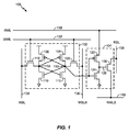
図1を参照すると、デバイスの特定の例示的な実施形態が示され、全体が100と表される。デバイス100は、スタティックランダムアクセスメモリ(SRAM)セル102を含む。デバイス100は、SRAMセル102に結合されたリードバッファ104をさらに含む。
With reference to FIG. 1, a particular exemplary embodiment of a device is shown and is generally designated 100.
SRAMセル102は、1対の交差結合インバータを含み得る。たとえば、図1では、SRAMセル102は、n型金属酸化物半導体電界効果トランジスタ(nMOSFET)110に結合されたp型金属酸化物半導体電界効果トランジスタ(pMOSFET)106によって形成された第1のインバータを含む。第1のインバータは、nMOSFET112に結合されたpMOSFET108によって形成された第2のインバータと交差結合する。pMOSFET106は、ノード114を介してnMOSFET110に結合される。pMOSFET108は、ノード116を介してnMOSFET112に結合される。
SRAMセル102は、複数のアクセストランジスタをさらに含み得る。たとえば、SRAMセル102は、アクセストランジスタ118およびアクセストランジスタ120を含む。アクセストランジスタ118は、書込みビット線(WBL)134に結合される。アクセストランジスタ118は、書込みワード線(WWL)132にさらに結合される。アクセストランジスタ120は、書込みワード線132および相補書込みビット線(WBLB)136に結合される。図1の特定の例では、SRAMセル102は、図示するように、6トランジスタ(6T)構成を有する。さらなる実施形態によれば、SRAMセル102は、図1の例とは異なる構成となる場合がある。
リードバッファ104は、SRAMセル102の出力部に結合され得る。たとえば、リードバッファ104は、ノード116に結合され得る。他の構成によれば、リードバッファ104は、ノード114に結合され得る。リードバッファ104は、スイッチおよびインバータを含む。たとえば、リードバッファ104は、nMOSFET124に結合されたpMOSFET122によって形成されたインバータに応答するスイッチ126を含み得る。図1に示すように、スイッチ126は、nMOSFETを含み得る。スイッチが、1つまたは複数の他の構造体を使用して実装され得ることを当業者は認識されよう。図1に示すように、リードバッファ104は、3つのトランジスタを含む、3トランジスタ(3T)構成として実装され得る。したがって、デバイス100は、図1の例に示すように、9トランジスタ(9T)構成として実装され得る。
Read
スイッチ126の制御端子は、リードバッファ104のインバータの出力部に応答し得る。たとえば、スイッチ126の制御端子128(たとえば、ゲート端子)は、pMOSFET122のドレイン端子とnMOSFET124のドレイン端子とに結合され得る。制御端子128は、図1の例に示すように、インバータの出力部に直接結合される(たとえば、接続される)ことによってインバータの出力部に応答し得る。別の例として、制御端子128は、制御端子128とインバータの出力部との間に別のデバイス構成要素が結合される場合など、インバータの出力部に間接的に結合されることによってインバータの出力部に応答し得る。インバータの入力部(たとえば、pMOSFET122のゲート端子とnMOSFET124のゲート端子との間の接続部)は、SRAMセルの出力部(たとえば、ノード116)に応答し得る。pMOSFET122のソース端子は、読出しワード線(RWL)130に結合され得る。nMOSFET124のソース端子は、接地ノード(たとえば、VSS)に結合され得る。
The control terminal of
スイッチ126は、読出しビット線(RBL)138などのビット線に結合され得る。スイッチ126は、相補読出しワード線(RWLB)140などの電圧端子にさらに結合され得る。図1に示すように、スイッチ126は、読出しビット線138と相補読出しワード線140との間に結合されたリードバッファ104の唯一の構成要素であり得る。加えて、図1に示した例では、スイッチ126のドレイン端子は読出しビット線138に結合され、スイッチ126のソース端子は相補読出しワード線140に結合される。
動作時に、読出し動作は、SRAMセル102のノード116に記憶された値を判定するためにデバイス100において始動され得る。読出し動作を始動するために、読出しビット線138は、論理高値(たとえば、VDD)にプリチャージされ得る。さらに、読出しワード線130は、論理高電圧に従ってバイアスされ、リードバッファ104のインバータを起動することができる。ノード116に記憶された値が論理低電圧(たとえば、0ビット)に相当する場合、リードバッファ104のインバータは、論理高電圧を生成するために論理低電圧を反転させる。インバータによって生成された論理高電圧は、スイッチ126の制御端子128をアクティブ化し得る。制御端子128が起動すると、スイッチ126は、プリチャージされた読出しビット線138を相補読出しワード線140に結合し、プリチャージされた読出しビット線138を放電し、論理低電圧(たとえば、0ビット)を有する読出しビットをもたらすことができる。したがって、読出し動作は、ノード116が論理低電圧(たとえば、0ビット)を記憶することを示すことができる。
In operation, a read operation can be initiated at
あるいは、ノード116に記憶された値が論理高電圧(たとえば、1ビット)に相当する場合、リードバッファ104のインバータは、論理低電圧を生成するために論理高電圧を反転させる。インバータによって生成された論理低電圧は、スイッチ126の制御端子128をアクティブ化しない。したがって、スイッチ126は、非アクティブ状態に維持される。したがって、プリチャージされた読出しビット線138は、スイッチ126が非アクティブ状態であるとき、相補読出しワード線140に放電されない。プリチャージされた読出しビット線138は、論理高電圧を保持し、論理高電圧(たとえば、1ビット)を有する読出しビットをもたらすことができる。したがって、読出し動作は、ノード116が論理高電圧(たとえば、1ビット)を記憶することを示すことができる。
Alternatively, if the value stored at
0ビットを読み出すとき、プリチャージされた読出しビット線138がリードバッファ104の単一の回路要素(すなわち、図1の例におけるスイッチ126)を介して放電されるので、感知遅延は、複数のトランジスタ(たとえば、直列に接続されたトランジスタ)を介して読出しビット線を放電する従来のデバイスと比較して改善される(すなわち、低減される)。たとえば、そのような複数のトランジスタは、キャパシタンスに関連付けられた充電遅延または放電遅延に基づいて0ビットの読出しを遅延させるキャパシタンスに関連付けられる場合がある。そのような遅延は、図1の特定の構成において低減または回避される。さらに、0ビットを読み出すとき、プリチャージされた読出しビット線138が単一の回路要素(すなわち、図1の例におけるスイッチ126)を介して放電されるので、リードバッファ104を通るセル電流(たとえば、Icell)は、複数のトランジスタを介して放電される従来のデバイスのセル電流よりも大きい。したがって、0ビットを読み出すことに関連付けられた感知遅延は、図1のデバイス100に関しては低減され得る。加えて、図1の構成は、図2を参照してさらに説明するように、SRAMセル102に記憶された1ビットを感知するとき、高い感知マージンを可能にし得る。
When reading a 0 bit, the sense delay is reduced by multiple transistors because the precharged
図2を参照すると、SRAMセル列の特定の例示的な実施形態が示され、全体が200と表される。図2は、図示の便宜上、SRAMセル列200として本明細書で説明するが、SRAMセル列200は、特定の用途に応じて様々な複数のSRAMセル(たとえば、SRAMセル行、またはSRAMセルの別の群)に相当し得ることを諒解されたい。
Referring to FIG. 2, a particular exemplary embodiment of a SRAM cell column is shown and is generally designated 200. FIG. 2 is described herein as an
SRAMセル列200のいくつかの構成要素については、図1を参照して説明され得る。たとえば、SRAMセル列200は、SRAMセル102およびリードバッファ104を含み得る。リードバッファ104は、ノード116を介してSRAMセル102に結合される。リードバッファ104は、スイッチ126と、pMOSFET122およびnMOSFET124によって形成されたインバータとを含む。スイッチ126は、制御端子128を含む。スイッチ126は、読出しビット線138および相補読出しワード線140に結合される。
Some components of the
SRAMセル列200は、1つまたは複数の追加のSRAMセルおよびリードバッファをさらに含み得る。たとえば、図2は、SRAMセル列200がSRAMセル202およびSRAMセル216をさらに含むことを示す。SRAMセル列200が、図2に示す特定の例とは異なる数のSRAMセルを含み得ることを諒解されたい。たとえば、様々な実施形態によれば、SRAMセル列200は、数百または数千のSRAMセルおよびリードバッファを含み得る。
The
SRAMセル202は、ノード206を介してリードバッファ204に結合される。リードバッファ204は、制御端子214を有するスイッチ212を含む。リードバッファ204は、nMOSFET210に結合されたpMOSFET208によって形成されたインバータをさらに含む。スイッチ212は、読出しビット線138に結合され、相補読出しワード線140にさらに結合される。
SRAMセル216は、ノード220を介してリードバッファ218に結合される。リードバッファ218は、制御端子228を有するスイッチ226を含む。スイッチ226の制御端子228は、nMOSFET224に結合されたpMOSFET222によって形成されたインバータに結合される。スイッチ226は、読出しビット線138に結合される場合があり、相補読出しワード線230にさらに結合される場合がある。
動作時に、読出し動作は、ノード116に記憶された値を判定するためにSRAMセル102において始動され得る。読出し動作を始動することは、読出しビット線138をプリチャージすることと、SRAMセル列200内の他のSRAMセルを選択解除することとを含み得る。たとえば、図2は、SRAMセル202、216がpMOSFET208、222のソース端子を接地することによって(たとえば、pMOSFET208、222に結合されたそれぞれの読出しワード線を接地電位にバイアスすることによって)選択解除されることを示す。他の動作中(たとえば、SRAMセル202、216を選択解除することを含まない他の動作中)、pMOSFET208、222のソース端子は、接地されずに、電源ノードに結合される場合がある。
In operation, a read operation can be initiated at
ノード116に記憶された値が(たとえば、「1読出し」動作中に)論理高電圧に相当する場合、リードバッファ104のインバータは、論理低電圧を生成するために論理高電圧を反転させる。論理低電圧は、制御端子128を非アクティブ化し(制御端子128を非アクティブ状態に維持し)、プリチャージされた読出しビット線138を相補読出しワード線140から分離する。プリチャージされた読出しビット線138が相補読出しワード線140から分離されている間、電流232は、スイッチ126を介して「漏洩する」場合がある。電流232は、スイッチ126を介してプリチャージされた読出しビット線138から相補読出しワード線140に流れる場合がある。制御端子128が非アクティブ化されるとき、電流232は、大きさIleakを有する漏洩電流に相当し得る。制御端子128がアクティブ化されるとき、電流232は、「読出し」電流に相当し得る(たとえば、スイッチ126が「オン」であるとき、電流232は、大きさIleakよりも大きい大きさを有し得る)。
If the value stored at
加えて、読出し動作中、電流234(たとえば、漏洩電流)は、スイッチ212を介してプリチャージされた読出しビット線138から相補読出しワード線140に流れる場合がある。たとえば、pMOSFET208のソース端子およびnMOSFET210のソース端子が接地されているので、制御端子214は、ノード206に記憶された値とは無関係に論理低電圧を介して非アクティブ化される。サブスレッショルド漏洩電流などの電流234は、スイッチ212が非アクティブ化されているにもかかわらずスイッチ212を通って流れる場合がある。したがって、リードバッファ104、204が、論理低電圧を有する共通の相補読出しワード線(すなわち、図2の例における相補読出しワード線140)に結合されているので、電流232、234は、共通の方向に(たとえば、図2に示すように、読出しビット線138から相補読出しワード線140の方に)流れる場合がある。
In addition, during a read operation, current 234 (eg, leakage current) may flow from read
SRAMセル列200の他のリードバッファは、相補読出しワード線140に結合されない場合がある。たとえば、図2は、リードバッファ218が相補読出しワード線140に結合されずに、代わりに相補読出しワード線230に結合されることを示す。読出し動作中、相補読出しワード線230は、論理高電圧(たとえば、VDD)に従って充電され、SRAMセル216が選択されないことを示す場合がある。したがって、リードバッファ218のスイッチ226は、接地されずに、論理高電圧に従って相補読出しワード線230にバイアスされる。したがって、リードバッファ218に関連付けられた電流236は、読出しビット線138の方に流れる場合がある。電流236は、大きさIleakを有し得る。
Other read buffers of the
さらに説明すれば、SRAMセル列200がn個のリードバッファに結合されたn個のセルを含む場合、(n-2)個のセルは、相補読出しワード線140に結合されたリードバッファを有しない。たとえば、リードバッファ218などの、リードバッファ104、204以外の、SRAMセル列200のリードバッファは、相補読出しワード線140に結合されない。したがって、SRAMセル列200の非選択のセルの漏洩電流の総量は、SRAMセル102に関連付けられた1読出し動作中、(n-2)*Ileakに相当し得る。したがって、大きさ(n-2)*Ileakを有する総漏洩電流は、SRAMセル102に関連付けられた1読出し動作中にプリチャージされた読出しビット線138「に」流れることによってプリチャージされた読出しビット線138の放電を妨害し、したがって、読出しビット線RBLのプリチャージを維持し、(たとえば、SRAMセル列200の他の構成要素から引き出される電流によって生じる電圧降下などの、読出しビット線138における電圧降下を防止または低減することによって)リードバッファ104から1ビットを読み出すときの感知マージンを改善する。
To further illustrate, if
加えて、各制御端子214、228は、図2に示すように、SRAMセル102に関連付けられた読出し動作中にノード206、220に記憶された値とは無関係に接地電位に維持される。たとえば、上述のように、pMOSFET208、222のソース端子は、SRAMセル102に関連付けられた読出し動作中に(たとえば、接地ノードに結合されることによって)接地され得る。pMOSFET208、222のソース端子を接地することによって、制御端子214、228は、ノード206、220に記憶された値とは無関係に非アクティブ化される。
In addition, each
ノード116に記憶された値が論理低電圧(たとえば、0ビット)に相当する場合、リードバッファ104のインバータは、論理高電圧を生成するために論理低電圧を反転させる。論理高電圧は、スイッチ126の制御端子128をアクティブ化し、スイッチ126を介してプリチャージされた読出しビット線138を相補読出しワード線140に結合する。プリチャージされた読出しビット線138を相補読出しワード線140に結合することは、電流232を介してプリチャージされた読出しビット線138を放電する。したがって、スイッチ126がアクティブ化されるとき、電流232は、大きさIleakよりも高い「読出し」大きさ(たとえば、Icell)を有し得る。電流232は、スイッチ126を介してプリチャージされた読出しビット線138から相補読出しワード線140に流れ、論理低値(たとえば、0ビット)を有する読出しビットをもたらすことができる。0ビットを読み出す間、SRAMセル列200内の非選択のSRAMセルの動作は、1読出し動作に関して上述したように動作し得る。たとえば、電流234、236(たとえば、大きさIleakを有する漏洩電流)は、それぞれ、リードバッファ204、218において生成され得る。0読出し動作中に、制御端子214、228は、1読出し動作に関して上述したように、ノード206、220に記憶された値とは無関係に非アクティブ状態に維持され得る。
If the value stored at
リードバッファ104から1ビットが読み出される間、SRAMセル列200内の1つまたは複数の非選択SRAMセル(たとえば、SRAMセル216)に関連付けられた漏洩電流が読出しビット線138に電流を放電するので、1ビットを読み出すときの感知マージンは(たとえば、読出しビット線138から流れ出る漏洩電流によって生じる読出しビット線138における電圧降下を防止または低減することによって)改善される。たとえば、読出しビット線138は、1読出し動作中にVDDに維持され得る。したがって、1読出し動作に関連付けられた感知マージンは、各非選択SRAMセルがプリチャージされた読出しビット線から電流を漏洩させる従来のデバイスと比較して改善される。図2を参照しながら説明する技法は、1読出し動作中にプリチャージされたビット線から流れ出る漏洩電流のために感知マージンが低下する従来のSRAM構成と比較してSRAMセル102に関連付けられた比較的大きいオン電流対オフ電流比Ion/Ioffを可能にし得る。したがって、SRAMセル列200における性能は、従来のデバイスと比較して増加したオン電流対オフ電流比Ion/Ioffにより改善される。
While one bit is read from the read
図3を参照すると、デバイスのレイアウトの特定の例示的な実施形態が示され、全体が300と表される。図3では、デバイス300のトランジスタは、複数の材料(たとえば、集積回路の層)を使用して形成され得る。たとえば、図3は、例示的なドープ領域402(たとえば、半導体基板のドープ領域)を示す。別の例として、図3は、ゲート領域404(たとえば、トランジスタゲート領域のポリシリコン領域および/またはゲート酸化物領域)を示す。図3のデバイス300の1つまたは複数の構造体は、相互接続部406などの相互接続部を介して結合され得る。さらに、デバイス300は、接点408などの、デバイス300の一部分を結合する1つまたは複数の接点を含み得る。
Referring to FIG. 3, a specific exemplary embodiment of a device layout is shown and is generally designated 300. In FIG. 3, the transistors of
デバイス300は、領域410、412、414、416を含む。特定の実施形態では、領域410、412、414、416の各々は、SRAMセルおよび対応するリードバッファのデバイス(たとえば、トランジスタ)に相当する。説明のために、領域410は、pMOSFET106、108、122、nMOSFET110、112、124、アクセストランジスタ118、120、およびスイッチ126を含み得る。別の例として、領域412は、pMOSFET208、nMOSFET210、およびスイッチ212を含み得る。別の例として、領域414は、pMOSFET222、nMOSFET224、およびスイッチ226を含み得る。
図3の例では、領域410、412は、相補読出しワード線140などの、共通の相補読出しワード線を介して結合された隣接するSRAMセルに相当する。領域414、416は、相補読出しワード線230などの、異なる共通の相補読出しワード線を介して結合されたリードバッファを有する隣接するSRAMセルに相当する。特定の例示的な実施形態では、デバイス300は、SRAMセル列200の一部分のレイアウト図に相当する。
In the example of FIG. 3,
図3は、デバイス300が集積回路の比較的少数の層を使用して効率的に実装され得ることを示す。したがって、デバイスの高さ(たとえば、デバイス300に相当するSRAMデバイスの「セル高さ」)は、比較的多くの集積回路層を使用して形成される従来のSRAMデバイスと比較して低減され得る。セル高さを低減することによって、キャパシタンス(たとえば、ビット線キャパシタンス)は、デバイス300では従来のデバイスと比較して低減され、したがって、(たとえば、従来のSRAMデバイスと比較してビット線を充電する必要時間を少なくすることによって)より速い動作を可能にし得る。さらに、リードバッファの対をそれぞれの相補読出しワード線に結合することによって、回路面積および回路構成要素の数は、各リードバッファが固有の相補読出しワード線に結合されたデバイスと比較して低減され得る。たとえば、リードバッファの対をそれぞれの相補読出しワード線に結合することによって、デバイス300を含む集積回路は、各リードバッファが固有の相補読出しワード線に結合された従来の集積回路よりも少数の金属層を含み得る。
FIG. 3 shows that the
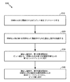
図4を参照すると、SRAMセルを動作させる方法の特定の例示的な実施形態が示され、全体が400と表される。SRAMセルは、SRAMセル102などの、図1〜図3を参照しながら説明するSRAMセルのうちのいずれかに相当し得る。方法400は、410において、SRAMセルにアクセスする前にビット線をプリチャージするステップを含み得る。一例として、ビット線は、読出しビット線138に相当し得る。
Referring to FIG. 4, a particular exemplary embodiment of a method of operating an SRAM cell is shown and is generally designated 400. The SRAM cell may correspond to any of the SRAM cells described with reference to FIGS. 1-3, such as
方法400は、420において、SRAMセルに関連付けられた読出し動作を始動するステップをさらに含み得る。特定の例として、読出しワード線130は、リードバッファ104のインバータをアクティブ化するために論理高電圧に従って充電され得る。別の例として、pMOSFET208、222のソース端子は、(たとえば、それぞれの読出しワード線を介して)接地され得る。
The
方法400は、430において、反転値を生成するためにSRAMセルに記憶された値を反転させるステップをさらに含み得る。この値は、SRAMセルに関連付けられたリードバッファのインバータによって反転される。リードバッファは、リードバッファ104に相当し得る。インバータは、pMOSFET122およびnMOSFET124を含み得る。この値は、ノード116に記憶され得る。
The
方法400は、440において、反転値に基づいてリードバッファのスイッチの制御端子を制御するステップをさらに含み得る。たとえば、スイッチの制御端子は、インバータの出力部に結合されるか、またはさもなければインバータの出力部に応答し得る。一例として、スイッチはスイッチ126に相当する場合があり、制御端子は制御端子128に相当する場合がある。インバータの出力部は、pMOSFET122のドレイン端子と、nMOSFET124のドレイン端子との間の接続部に相当し得る。
The
方法400は、450において、ビット線の論理値に基づいて読出しビットを判定するステップをさらに含み得る。たとえば、反転値が論理1値に相当する場合、スイッチの制御端子を制御するステップは、スイッチをアクティブ化することによってプリチャージされたビット線を電圧端子に放電するステップを含み得る。電圧端子は、相補読出しワード線140に相当し得る。スイッチをアクティブ化しプリチャージされたビット線を放電するステップは、ビット線において論理0値を生成し得る。したがって、スイッチをアクティブ化することは、0読出しビットをもたらす。
The
別の例として、反転値が論理0値に相当する場合、スイッチの制御端子を制御するステップは、スイッチを非アクティブ状態に維持するステップを含み得る。スイッチを非アクティブ状態に維持するステップは、ビット線において論理1値をもたらし得る(たとえば、ビット線は、プリチャージを保持し、スイッチを介して電圧端子に放電されない)。スイッチを非アクティブ状態に維持するステップは、1読出しビットをもたらす。
As another example, when the inverted value corresponds to a logical zero value, controlling the control terminal of the switch may include maintaining the switch in an inactive state. Maintaining the switch in an inactive state can result in a
図4の方法400は、SRAMセルに記憶された0ビット値を感知することに関連付けられた低い感知遅延を可能にし得る。たとえば、0読出し動作中に単一のスイッチを介してプリチャージされたビット線を迅速に放電することによって、0ビット値を感知することに関連付けられた感知遅延は、直列に接続されたトランジスタを利用する従来のSRAMデバイスと比較して減少され得る。さらに、本明細書で説明する技法は、図5を参照しながらさらに説明するように、複数のSRAMセル(たとえば、SRAMセル列)の1つまたは複数の漏洩電流を利用することなどによって、1ビット値を感知することに関連付けられた感知マージンを改善し得る。
The
加えて、SRAMセルに記憶されたビット値を判定した後、1つまたは複数の追加の動作が、SRAMセルを含むメモリデバイス(たとえば、SRAMアレイ)において実行され得る。たとえば、メモリデバイスの1つまたは複数のSRAMセルは、読出し動作、書込み動作、またはそれらの組合せに対して選択され得る。代替的にまたは追加として、メモリデバイスに関連付けられた待機動作モードが始動され得る。制御端子は、待機動作モード中、非アクティブ状態に維持される。たとえば、スイッチの制御端子は、待機動作モード中、論理0値にバイアスされ得る。待機動作モードは、読出し動作を実行した後、およびメモリデバイスにおいて追加の読出し動作も書込み動作も起こるようにはスケジューリングされていないと判定したときなど、メモリデバイスが非アクティブであるとき、始動され得る。待機動作モードは、メモリデバイスの各SRAMセルに対して始動され得る。 In addition, after determining the bit value stored in the SRAM cell, one or more additional operations may be performed in a memory device (eg, an SRAM array) that includes the SRAM cell. For example, one or more SRAM cells of the memory device may be selected for a read operation, a write operation, or a combination thereof. Alternatively or additionally, a standby mode of operation associated with the memory device may be initiated. The control terminal is maintained in an inactive state during the standby operation mode. For example, the control terminal of the switch can be biased to a logic zero value during the standby mode of operation. The standby mode of operation may be initiated when the memory device is inactive, such as after performing a read operation and when it is determined that no additional read or write operations are scheduled in the memory device. . A standby mode of operation may be initiated for each SRAM cell of the memory device.
特定の実施形態では、リードバッファのトランジスタは、待機動作モード中、トランジスタの各々のドレインソース間電圧(VDS)が0になるようにバイアスされる。たとえば、待機動作モード中、pMOSFET122のソース端子およびnMOSFET124のソース端子は、共通の電圧に(たとえば、接地電圧に)バイアスされ得る。さらに、読出しビット線138および相補読出しワード線140は、待機動作モード中、共通の電圧に(たとえば、VDDに)バイアスされ、したがって、待機動作モード中、スイッチ126の端子(たとえば、ソース端子およびドレイン端子)を共通の電圧に維持することができる。
In certain embodiments, the transistors in the read buffer are biased so that the drain-source voltage (V DS ) of each of the transistors is zero during the standby mode of operation. For example, during the standby mode of operation, the source terminal of
したがって、リードバッファのトランジスタのドレインソース間電圧は、待機動作モード中、ほぼ0であり、待機動作モード中には読出し動作中と比較してリードバッファを通る漏洩電流を低減することができる。したがって、「サブスレッショルド」漏洩電流または「スタティック」漏洩電流を含む、待機動作中にリードバッファを通る漏洩電流は、低減または除去される。たとえば、リードバッファを通る漏洩電流は、待機動作中に読出しビット線からリードバッファまで漏洩電流が流れる、従来のSRAM構成と比較して低減される。待機動作モードを使用して漏洩電流を低減することは、モバイルデバイスのバッテリ電力などの電力を節約することができる。 Accordingly, the drain-source voltage of the transistor of the read buffer is substantially 0 during the standby operation mode, and the leakage current passing through the read buffer can be reduced during the standby operation mode as compared with during the read operation. Thus, leakage current through the read buffer during standby operation, including “sub-threshold” leakage current or “static” leakage current, is reduced or eliminated. For example, leakage current through the read buffer is reduced compared to a conventional SRAM configuration in which leakage current flows from the read bit line to the read buffer during standby operation. Reducing leakage current using the standby mode of operation can save power, such as battery power of the mobile device.
図5を参照すると、SRAMセル列を動作させる方法の特定の例示的な実施形態が示され、全体が500と表される。SRAMセル列は、図2のSRAMセル列200に相当し得る。方法500は、510において、SRAMセル列に関連付けられたビット線をプリチャージするステップを含み得る。ビット線は、図1の読出しビット線138に相当し得る。
Referring to FIG. 5, a particular exemplary embodiment of a method for operating an SRAM cell column is shown and is generally designated 500. The SRAM cell column may correspond to the
520において、SRAMセル列の第1のSRAMセルに関連付けられた読出し動作が始動され得る。第1のSRAMセルは、SRAMセル102などの、図1および図2を参照しながら説明するSRAMセルのうちのいずれかに相当し得る。530において、読出し動作中、第1の漏洩電流が、ビット線から、SRAMセル列の第1の非選択SRAMセルの第1のリードバッファに流れる場合がある。たとえば、第1のリードバッファおよび第1の非選択SRAMセルは、それぞれ、リードバッファ204およびSRAMセル202に相当し得る。第1の漏洩電流は、電流234に相当し得る。
At 520, a read operation associated with the first SRAM cell of the SRAM cell column can be initiated. The first SRAM cell may correspond to any of the SRAM cells described with reference to FIGS. 1 and 2, such as SRAM cell. At 530, during the read operation, the first leakage current may flow from the bit line to the first read buffer of the first unselected SRAM cell in the SRAM cell column. For example, the first read buffer and the first unselected SRAM cell may correspond to the read
540において、読出し動作中、第2の漏洩電流が、SRAMセル列の第2の非選択SRAMセルの第2のリードバッファから、ビット線に流れる場合がある。第2のリードバッファおよび第2のSRAMセルは、リードバッファ218およびSRAMセル216に相当し得る。第2の漏洩電流は、電流236に相当し得る。特定の実施形態では、第1の漏洩電流および第2の漏洩電流は各々、大きさIleakを有する。SRAMセル列がnSRAMセルを含む場合、ビット線に流れる漏洩電流の総量は、図2を参照しながら説明したように、(n-2)*Ileakに相当し得る。
In 540, during the read operation, the second leakage current may flow from the second read buffer of the second unselected SRAM cell of the SRAM cell column to the bit line. The second read buffer and the second SRAM cell may correspond to the read
大きさ(n-2)*Ileakを有する総漏洩電流は、第1のSRAMセルに関連付けられた読出し動作中にビット線に流れるので、ビット線のプリチャージは、1読出し動作中、維持され得る。したがって、1読出し動作中の感知マージンは、ビット線においてプリチャージを維持する総漏洩電流により改善され得る。たとえば、感知マージンは、1読出し動作中、漏洩電流がビット線の放電(または、部分的な放電)をもたらす、従来のデバイスと比較して改善され得る。0読出し中の感知遅延も、いくつかの従来のSRAMデバイスと比較して改善される。たとえば、0読出し動作中の感知遅延は、0読出し動作中、非選択のSRAMセルからの漏洩電流がビット線に流れる、従来のSRAM「バッファフット」リードバッファ構成と比較して改善される。1読出し動作中の感知マージンおよび0読出し動作中の感知遅延が各々改善されるので、図5を参照しながら説明する技法は、SRAM性能の改善を可能にし、電子デバイスのより良い性能をもたらすことができる。 The total leakage current with magnitude (n-2) * I leak flows through the bit line during the read operation associated with the first SRAM cell, so the bit line precharge is maintained during one read operation. obtain. Therefore, the sensing margin during one read operation can be improved by the total leakage current that maintains the precharge in the bit line. For example, the sensing margin may be improved compared to conventional devices where leakage current results in bit line discharge (or partial discharge) during one read operation. 0 Sensing delay during reading is also improved compared to some conventional SRAM devices. For example, sense delay during a zero read operation is improved compared to a conventional SRAM “buffer foot” read buffer configuration in which leakage current from unselected SRAM cells flows through the bit line during a zero read operation. Since the sensing margin during 1 read operation and the sensing delay during 0 read operation are each improved, the technique described with reference to FIG. 5 allows for improved SRAM performance and results in better performance of electronic devices. Can do.
図4の方法400および図5の方法500の一方または両方は、SRAMメモリデバイスを含むか、またはそれにアクセスする電子デバイスの回路または構成要素において実行され得る。たとえば、図4の方法400および図5の方法500の一方または両方は、SRAMメモリデバイスを含むか、もしくはそれにアクセスするフィールドプログラマブルゲートアレイ(FPGA)デバイス、SRAMメモリデバイスを含むか、もしくはそれにアクセスする特定用途向け集積回路(ASIC)、SRAMメモリデバイスを含むか、もしくはそれにアクセスする中央処理ユニット(CPU)などの処理ユニット、SRAMメモリデバイスを含むか、もしくはそれにアクセスするデジタル信号プロセッサ(DSP)、SRAMメモリデバイスを含むか、もしくはそれにアクセスするコントローラ、SRAMメモリデバイスを含むか、もしくはそれにアクセスする別のハードウェアデバイス、SRAMメモリデバイスを含むか、もしくはそれにアクセスするファームウェアデバイス、またはそれらの組合せにおいて実行され得る。一例として、図4の方法400および図5の方法500の一方または両方は、図6に関して説明するように、命令を実行するプロセッサにおいて実行され得る。
One or both of the
図6を参照すると、モバイルデバイスの特定の例示的な実施形態のブロック図が示され、全体が600と表される。モバイルデバイス600は、デジタル信号プロセッサ(DSP)などのプロセッサ610を含む。図6の例では、プロセッサ610は、図1のデバイス100を含む。デバイス100は、SRAMアレイ612に含まれ得る。SRAMアレイ612は、プロセッサ610のキャッシュに相当し得る。他の実施形態によれば、デバイス100は、モバイルデバイス600の別の位置に含まれ得る。たとえば、SRAMアレイ612は、プロセッサ610の外部にある場合がある。別の例として、デバイス100は、図6に示す特定の例と比較してモバイルデバイス600の異なる構成要素に含まれ得る。プロセッサ610は、SRAMアレイ612においていくつかの動作を始動することができる。たとえば、プロセッサ610は、SRAMアレイ612のSRAMセルにおいて読出し動作を始動することができる。
Referring to FIG. 6, a block diagram of a particular exemplary embodiment of a mobile device is shown and is generally designated 600.
プロセッサ610は、メモリ632(たとえば、非一時的コンピュータ可読媒体)に結合され得る。メモリ632は、命令654、データ656、またはそれらの組合せを記憶することができる。命令654は、本明細書で説明する1つまたは複数の動作を実行するために、プロセッサ610によって実行可能とすることができる。たとえば、命令654は、デバイス100のSRAMセル102にアクセスすることを含むメモリ動作を実行するために(たとえば、デバイス100のSRAMセル102において読出し動作を始動するために)プロセッサ610によって実行可能とすることができる。たとえば、命令654は、図4を参照しながら説明した待機動作モードなどの待機動作モードにSRAMアレイ612を入れるためにプロセッサ610によって実行可能とすることができる。特定の実施形態では、SRAMアレイ612は、命令654、データ656、またはそれらの組合せの一部分を記憶するように構成されたキャッシュ(たとえば、命令キャッシュ、データキャッシュ、またはそれらの組合せ)に相当する。
The
図6は、プロセッサ610およびディスプレイ628に結合されたディスプレイコントローラ626も示す。コーダ/デコーダ(コーデック)634も、プロセッサ610に結合することができる。スピーカ636およびマイクロフォン638は、コーデック634に結合することができる。モバイルデバイス600は、プロセッサ610およびカメラ646に結合されたカメラコントローラ690をさらに含み得る。図6は、ワイヤレスコントローラ640が、プロセッサ610および無線周波数(RF)インターフェース650(たとえば、トランシーバ)に結合され得ることも示す。RFインターフェース650は、アンテナ642に結合され得る。
FIG. 6 also shows a
特定の実施形態では、プロセッサ610、ディスプレイコントローラ626、カメラコントローラ690、メモリ632、コーデック634、およびワイヤレスコントローラ640は、システムインパッケージまたはシステムオンチップデバイス622に含まれる。特定の実施形態では、入力デバイス630および電源644は、システムオンチップデバイス622に結合される。さらに、特定の実施形態では、図6に示すように、ディスプレイ628、入力デバイス630、スピーカ636、マイクロフォン638、アンテナ642、カメラ646、RFインターフェース650、および電源644は、システムオンチップデバイス622の外部にある。しかしながら、ディスプレイ628、入力デバイス630、スピーカ636、マイクロフォン638、アンテナ642、カメラ646、RFインターフェース650、および電源644の各々は、インターフェースまたはコントローラなどの、システムオンチップデバイス622の構成要素に結合され得る。
In certain embodiments,
説明した実施形態と併せて、装置は、値を記憶するための手段(たとえば、SRAMセル102、202、216のうちのいずれか、またはSRAMアレイ612内の任意のSRAMセル)と、読出し動作中に値をバッファリングするための手段(たとえば、リードバッファ104、204、218のうちのいずれか)とを含む。値をバッファリングするための手段は、反転値を生成するために値を反転させるための手段(たとえば、リードバッファ104、204、218のインバータのうちのいずれか)を含む。値をバッファリングするための手段は、反転値に基づいてビット線(たとえば、読出しビット線138)を電圧端子(たとえば、相補読出しワード線140、230のうちのいずれか)に選択的に結合するための手段(たとえば、スイッチ126、212、226のうちのいずれか)をさらに含む。
In conjunction with the described embodiments, the apparatus is in a read operation with a means for storing values (eg, any of the
説明した実施形態と併せて、コンピュータ可読媒体(たとえば、メモリ632)は、SRAMセル(たとえば、SRAMセル102、202、216のうちのいずれか、またはSRAMアレイ612内の任意のSRAMセル)にアクセスするためにプロセッサ(たとえば、プロセッサ610)によって実行可能な命令(たとえば、命令654)を記憶する。SRAMセルにアクセスすることは、反転値を生成するためにSRAMセルに記憶された値を反転させることを含む。この値は、SRAMセルに関連付けられたリードバッファ(たとえば、リードバッファ104、204、218のうちのいずれか)のインバータ(たとえば、リードバッファ104、204、218のインバータのうちのいずれか)によって反転される。SRAMセルにアクセスすることは、反転値に基づいてリードバッファのスイッチ(たとえば、スイッチ126、212、226のうちのいずれか)の制御端子(たとえば、制御端子128、214、228のうちのいずれか)を制御することをさらに含む。
In conjunction with the described embodiments, a computer readable medium (eg, memory 632) accesses an SRAM cell (eg, any of
上記の開示されたデバイスおよび機能は、設計され、コンピュータ可読媒体上に記憶されたコンピュータファイル(たとえば、RTL、GDSII、GERBERなど)に構成され得る。そのようなファイルの一部またはすべてが、そのようなファイルに基づいてデバイスを製造する製造関係者に提供され得る。得られる製品としては、次いで半導体ダイに切断されて半導体チップへパッケージングされる半導体ウェハが含まれる。次いで、チップは、モバイルデバイス600などの上述したデバイス内に採用される。図7は、電子デバイス製造プロセス700の特定の例示的な実施形態を示す。特定の例として、半導体ダイは、図1のデバイス100を含み得る。
The disclosed devices and functions described above can be configured into computer files (eg, RTL, GDSII, GERBER, etc.) that are designed and stored on a computer-readable medium. Some or all of such files may be provided to manufacturing personnel who manufacture devices based on such files. The resulting product includes a semiconductor wafer that is then cut into semiconductor dies and packaged into semiconductor chips. The chip is then employed in a device as described above, such as
図7を参照すると、物理デバイス情報702が、調査コンピュータ706などの製造プロセス700において受け取られる。物理的デバイス情報702は、図1のデバイス100、図2のSRAMセル列200、図3のデバイス300、またはそれらの組合せなどの、インバータおよびスイッチを有するリードバッファに結合されたSRAMセルを含む半導体デバイスの少なくとも1つの物理的特性を表す設計情報を含み得る。たとえば、物理デバイス情報702は、調査コンピュータ706に結合されたユーザインターフェース704を介して入力される物理パラメータ、材料特性、および構造情報を含み得る。調査コンピュータ706は、メモリ710などのコンピュータ可読媒体に結合された、1つまたは複数の処理コアなどのプロセッサ708を含む。メモリ710は、プロセッサ708に、ファイルフォーマットに従うように物理デバイス情報702を変換させ、ライブラリファイル712を生成させるために実行可能なコンピュータ可読命令を記憶することができる。
With reference to FIG. 7,
特定の実施形態では、ライブラリファイル712は、変換された設計情報を含む少なくとも1つのデータファイルを含む。たとえば、ライブラリファイル712は、電子設計自動化(EDA)ツール720とともに使用するために提供される、図1のデバイス100、図2のSRAMセル列200、図3のデバイス300、またはそれらの組合せなどの、インバータおよびスイッチを有するリードバッファに結合されたSRAMセルを含むデバイスを含む半導体デバイスのライブラリを含み得る。
In certain embodiments, the
ライブラリファイル712は、メモリ718に結合された、1つまたは複数の処理コアなどのプロセッサ716を含む設計用コンピュータ714においてEDAツール720とともに使用され得る。EDAツール720は、設計用コンピュータ714のユーザが、図1のデバイス100、図2のSRAMセル列200、図3のデバイス300、またはそれらの組合せなどの、インバータおよびスイッチを有するリードバッファに結合されたSRAMセルを含む回路を設計することを可能にするためにメモリ718においてプロセッサ実行可能命令として記憶され得る。たとえば、設計用コンピュータ714のユーザは、設計用コンピュータ714に結合されたユーザインターフェース724を介して回路設計情報722を入力することができる。回路設計情報722は、図1のデバイス100、図2のSRAMセル列200、図3のデバイス300、またはそれらの組合せなどの、インバータおよびスイッチを有するリードバッファに結合されたSRAMセルなどの半導体デバイスの少なくとも1つの物理的特性を表す設計情報を含み得る。説明のために、回路設計特性は、特定の回路の識別と回路設計における他の要素との関係、位置決め情報、特徴サイズ情報、相互接続情報、または半導体デバイスの物理的特性を表す他の情報を含み得る。
設計用コンピュータ714は、回路設計情報722を含む設計情報をファイルフォーマットに準拠するように変換するように構成され得る。説明のために、ファイルフォーメーションは、平面幾何形状、テキストラベル、およびグラフィックデータシステム(GDSII)ファイルフォーマットなどの階層フォーマット内の回路レイアウトに関する他の情報を表すデータベースバイナリファイルフォーマットを含み得る。設計用コンピュータ714は、図1のデバイス100、図2のSRAMセル列200、図3のデバイス300、またはそれらの組合せなどの、インバータおよびスイッチを有するリードバッファに結合されたSRAMセルについて説明する情報を、他の回路または情報に加えて含む、GDSIIファイル726などの変換された設計情報を含むデータファイルを生成するように構成され得る。説明のために、データファイルは、図1のデバイス100、図2のSRAMセル列200、図3のデバイス300、またはそれらの組合せなどの、インバータおよびスイッチを有するリードバッファに結合されたSRAMセルを含むシステムオンチップ(SoC)に対応する情報を含み得る。データファイルは、SoC内の追加の電子回路および構成要素に関連付けられた情報をさらに含み得る。SoCは、図6のシステムオンチップデバイス622に相当し得る。
GDSIIファイル726は、GDSIIファイル726内の変換情報に従って、図1のデバイス100、図2のSRAMセル列200、図3のデバイス300、またはそれらの組合せなどの、インバータおよびスイッチを有するリードバッファに結合されたSRAMセルを製造するために製造プロセス728において受け取られ得る。たとえば、デバイス製造プロセスは、代表的なマスク732として示された、フォトリソグラフィプロセスとともに使用されるマスクなどの、1つまたは複数のマスクを作製するために、マスク製造業者730にGDSIIファイル726を供給することを含み得る。マスク732は、試験され、代表的なダイ736などのダイに分離され得る1つまたは複数のウェハ734を生成するために、製造プロセス中に使用され得る。ダイ736は、図1のデバイス100、図2のSRAMセル列200、図3のデバイス300、またはそれらの組合せなどの、インバータおよびスイッチを有するリードバッファに結合されたSRAMセルを含むデバイスを含む。
GDSII file 726 is coupled to a read buffer having an inverter and a switch, such as
ダイ736は、パッケージングプロセス738に供給される場合があり、ダイ736は、代表的なパッケージ740に組み込まれる。たとえば、パッケージ740は、単一のダイ736またはシステムインパッケージ(SiP)配置などの複数のダイを含み得る。パッケージ740は、電子デバイス技術合同協議会(JEDEC)規格などの、1つまたは複数の規格または仕様に準拠するように構成され得る。
The
パッケージ740に関する情報は、コンピュータ746に記憶された構成要素ライブラリなどを介して、様々な製品設計者に配布され得る。コンピュータ746は、メモリ750に結合された、1つまたは複数の処理コアなどのプロセッサ748を含み得る。プリント回路基板(PCB)ツールは、ユーザインターフェース744を介してコンピュータ746のユーザから受け取られたPCB設計情報742を処理するために、メモリ750においてプロセッサ実行可能命令として記憶され得る。PCB設計情報742は、回路基板上のパッケージングされた半導体デバイスの物理的位置情報を含む場合があり、パッケージングされた半導体デバイスは、図1のデバイス100、図2のSRAMセル列200、図3のデバイス300、またはそれらの組合せなどの、インバータおよびスイッチを有するリードバッファに結合されたSRAMセルを含むパッケージ740に相当する。
Information regarding the
コンピュータ746は、回路基板上のパッケージングされた半導体デバイスの物理的位置情報とともに、配線およびビアなどの電気接続のレイアウトを含む、GERBERファイル752などのデータファイルを生成するために、PCB設計情報742を変換するように構成される場合があり、パッケージングされた半導体デバイスは、図1のデバイス100、図2のSRAMセル列200、図3のデバイス300、またはそれらの組合せなどの、インバータおよびスイッチを有するリードバッファに結合されたSRAMセルを含むパッケージ740に相当する。他の実施形態では、変換されたPCB設計情報によって生成されるデータファイルは、GERBERフォーマット以外のフォーマットを有し得る。
GERBERファイル752は、基板組立てプロセス754において受け取られ、GERBERファイル752内に記憶された設計情報に従って製造される、代表的なPCB756などのPCBを作製するために使用され得る。たとえば、GERBERファイル752は、PCB製造プロセスの様々なステップを実行するために、1つまたは複数のマシンにアップロードされ得る。PCB756は、代表的なプリント回路アセンブリ(PCA)758を形成するために、パッケージ740を含む電子構成要素を装着され得る。
The GERBER file 752 can be used to create a PCB, such as a
PCA758は、製品製造プロセス760において受け取られ、第1の代表的な電子デバイス762および第2の代表的な電子デバイス764などの、1つまたは複数の電子デバイスに統合され得る。例示的かつ非限定的な例として、第1の代表的な電子デバイス762、第2の代表的な電子デバイス764、またはこれらの両方は、モバイルデバイス、コンピュータ、タブレット、セットトップボックス、音楽プレーヤ、ビデオプレーヤ、娯楽ユニット、ナビゲーションデバイス、通信デバイス、携帯情報端末(PDA)、および固定位置データユニットから成る群から選択される場合があり、これらに、図1のデバイス100、図2のSRAMセル列200、図3のデバイス300、またはそれらの組合せなどの、インバータおよびスイッチを有するリードバッファに結合されたSRAMセルが統合される。別の例示的かつ非限定的な例として、電子デバイス762および764のうちの1つまたは複数は、モバイルフォン、ハンドヘルドパーソナル通信システム(PCS)ユニット、携帯情報端末などのポータブルデータユニット、全地球測位システム(GPS)対応デバイス、ナビゲーションデバイス、メーター読取り機器などの固定位置データユニット、またはデータもしくはコンピュータ命令を記憶しもしくは取り出す任意の他のデバイス、あるいはそれらの任意の組合せなどのリモートユニットであり得る。図7は、本開示の教示によるリモートユニットを示すが、本開示は、これらの図示のユニットに限定されない。本開示の実施形態は、メモリおよびオンチップ回路を含む能動集積回路を含む任意のデバイス内で適切に使用され得る。
The
図1のデバイス100、図2のSRAMセル列200、図3のデバイス300、またはそれらの組合せなどの、インバータおよびスイッチを有するリードバッファに結合されたSRAMセルを含むデバイスは、例示的なプロセス700で説明するように、作製され、処理され、電子デバイスに組み込まれ得る。図1〜図7を参照しながら説明する実施形態の1つまたは複数の態様は、ライブラリファイル712、GDSIIファイル726、およびGERBERファイル752内などの、様々な処理ステージにおいて含まれ、ならびに、調査コンピュータ706のメモリ710、設計用コンピュータ714のメモリ718、コンピュータ746のメモリ750、基板アセンブリプロセス754などの様々なステージにおいて使用される1つまたは複数の他のコンピュータまたはプロセッサ(図示せず)のメモリにおいて格納され、また、マスク732、ダイ736、パッケージ740、PCA758、プロトタイプ回路もしくはデバイス(図示せず)などの他の製品、またはそれらの任意の組合せなどの1つまたは複数の他の物理実施形態に組み込まれ得る。物理デバイス設計から最終製品までの生産の様々な代表的なステージが、図示されているが、他の実施形態では、より少数のステージが使用され得るか、または追加のステージが含まれ得る。同様に、プロセス700は、単一のエンティティによって、またはプロセス700の様々なステージを実行する1つまたは複数のエンティティによって実行され得る。
A device including SRAM cells coupled to a read buffer having an inverter and a switch, such as
当業者は、本明細書で開示する実施形態に関して説明する様々な例示的な論理ブロック、構成、モジュール、回路、およびアルゴリズムステップが、電子ハードウェアとして、プロセッサによって実行されるコンピュータソフトウェアとして、または両方の組合せとして実装され得ることをさらに諒解するであろう。様々な例示的な構成要素、ブロック、構成、モジュール、回路、およびステップについて、概してそれらの機能の観点から上記で説明されてきた。そのような機能がハードウェアまたはプロセッサ実行可能命令として実装されるかどうかは、特定の適用例および全体的なシステムに課された設計制約に依存する。当業者は、説明した機能を特定の応用例ごとに様々な形で実装することができるが、そのような実装の決定が本開示の範囲からの逸脱を引き起こすものと解釈されてはならない。 Those skilled in the art will recognize that the various exemplary logic blocks, configurations, modules, circuits, and algorithm steps described with respect to the embodiments disclosed herein may be implemented as electronic hardware, computer software executed by a processor, or both. It will be further appreciated that can be implemented as a combination of: Various illustrative components, blocks, configurations, modules, circuits, and steps have been described above generally in terms of their functionality. Whether such functionality is implemented as hardware or processor-executable instructions depends on the particular application and design constraints imposed on the overall system. Those skilled in the art can implement the described functionality in a variety of ways for each particular application, but such implementation decisions should not be construed as causing deviations from the scope of the present disclosure.
本明細書で開示する実施形態に関して説明する方法またはアルゴリズムのステップは、直接ハードウェア内で、プロセッサによって実行されるソフトウェアモジュール内で、またはこの2つの組合せにおいて具体化され得る。ソフトウェアモジュールは、ランダムアクセスメモリ(RAM)、フラッシュメモリ、読取り専用メモリ(ROM)、プログラム可能読取り専用メモリ(PROM)、消去可能プログラム可能読取り専用メモリ(EPROM)、電気的消去可能プログラム可能読取り専用メモリ(EEPROM)、レジスタ、ハードディスク、リムーバブルディスク、コンパクトディスク読取り専用メモリ(CD-ROM)、または当技術分野で既知の任意の他の形の非一時的記憶媒体内に存在し得る。例示的な記憶媒体は、プロセッサが記憶媒体から情報を読み出し、記憶媒体に情報を書き込むことができるように、プロセッサに結合される。代替形態において、記憶媒体はプロセッサと一体であり得る。プロセッサおよび記憶媒体は、特定用途向け集積回路(ASIC)内に存在し得る。ASICは、コンピューティングデバイスまたはユーザ端末内に存在し得る。代替として、プロセッサおよび記憶媒体は、コンピューティングデバイスまたはユーザ端末内に個別構成要素として存在し得る。 The method or algorithm steps described with respect to the embodiments disclosed herein may be embodied directly in hardware, in a software module executed by a processor, or in a combination of the two. Software modules include random access memory (RAM), flash memory, read only memory (ROM), programmable read only memory (PROM), erasable programmable read only memory (EPROM), electrically erasable programmable read only memory (EEPROM), registers, hard disk, removable disk, compact disk read only memory (CD-ROM), or any other form of non-transitory storage medium known in the art. An exemplary storage medium is coupled to the processor such that the processor can read information from, and write information to, the storage medium. In the alternative, the storage medium may be integral to the processor. The processor and the storage medium may reside in an application specific integrated circuit (ASIC). The ASIC may reside in a computing device or user terminal. In the alternative, the processor and the storage medium may reside as discrete components in a computing device or user terminal.
開示されている実施形態の前述の説明は、当業者が開示されている実施形態を作製または使用することを可能にするために提供されている。これらの実施形態に対する様々な修正は、当業者には容易に明らかであり、本明細書で定義されている原理は、本開示の範囲から逸脱することなく、他の実施形態に適用され得る。したがって、本開示は、本明細書に示されている実施形態に限定されることを意図されておらず、以下の特許請求の範囲によって定義される原理および新規な特徴と一致する最も広い範囲を与えられるべきである。 The previous description of the disclosed embodiments is provided to enable any person skilled in the art to make or use the disclosed embodiments. Various modifications to these embodiments will be readily apparent to those skilled in the art, and the principles defined herein may be applied to other embodiments without departing from the scope of the disclosure. Accordingly, this disclosure is not intended to be limited to the embodiments shown herein, but is to be accorded the widest scope consistent with the principles and novel features defined by the following claims. Should be given.
100 デバイス
102 SRAMセル
104 リードバッファ
106 pMOSFET
108 pMOSFET
110 nMOSFET
112 nMOSFET
114 ノード
116 ノード
118 アクセストランジスタ
120 アクセストランジスタ
122 pMOSFET
124 nMOSFET
126 スイッチ
128 制御端子
130 読出しワード線
132 書込みワード線
134 書込みビット線
136 相補書込みビット線
138 読出しビット線
140 相補読出しワード線
200 SRAMセル列
202 SRAMセル
204 リードバッファ
206 ノード
208 pMOSFET
210 nMOSFET
212 スイッチ
214 制御端子
216 SRAMセル
218 リードバッファ
220 ノード
222 pMOSFET
224 nMOSFET
226 スイッチ
228 制御端子
230 相補読出しワード線
232 電流
234 電流
236 電流
300 デバイスのレイアウト
402 ドープ領域
404 ゲート領域
406 相互接続部
408 接点
410 領域
412 領域
414 領域
416 領域
600 モバイルデバイス
610 プロセッサ
612 SRAMアレイ
622 システムインパッケージ、システムオンチップデバイス
626 ディスプレイコントローラ
628 ディスプレイ
630 入力デバイス
632 メモリ
634 コーデック
636 スピーカ
638 マイクロフォン
640 ワイヤレスコントローラ
642 アンテナ
644 電源
646 カメラ
650 RFインターフェース
654 命令
656 データ
690 カメラコントローラ
700 製造プロセス
702 物理デバイス情報
704 ユーザインターフェース
706 調査コンピュータ
708 プロセッサ
710 メモリ
712 インバータおよびスイッチを有するリードバッファに結合されたSRAMセルを含むライブラリファイル
714 設計用コンピュータ
716 プロセッサ
718 メモリ
720 EDAツール
722 回路設計情報
724 ユーザインターフェース
726 インバータおよびスイッチを有するリードバッファに結合されたSRAMセルを含むGDSIIファイル
728 製造プロセス
730 マスク製造業者
732 マスク
734 ウェハ
736 ダイ
738 パッケージングプロセス
740 パッケージ
742 PCB設計情報
744 ユーザインターフェース
746 コンピュータ
748 プロセッサ
750 メモリ
752 インバータおよびスイッチを有するリードバッファに結合されたSRAMセルを含むGERBERファイル
754 基板組立て
756 プリント回路基板(PCB)
758 プリント回路アセンブリ(PCA)
760 製品製造者
762 電子デバイス1
764 電子デバイス2
100 devices
102 SRAM cell
104 Read buffer
106 pMOSFET
108 pMOSFET
110 nMOSFET
112 nMOSFET
114 nodes
116 nodes
118 Access transistor
120 Access transistor
122 pMOSFET
124 nMOSFET
126 switch
128 Control terminal
130 Read word line
132 Write word line
134 Write bit line
136 Complementary write bit line
138 Read bit line
140 Complementary read word line
200 SRAM cell array
202 SRAM cell
204 Read buffer
206 nodes
208 pMOSFET
210 nMOSFET
212 switch
214 Control terminal
216 SRAM cell
218 Read buffer
220 nodes
222 pMOSFET
224 nMOSFET
226 switch
228 Control terminal
230 Complementary read word line
232 current
234 current
236 current
300 device layout
402 doped region
404 gate area
406 Interconnection
408 contacts
410 area
412 area
414 area
416 area
600 mobile devices
610 processor
612 SRAM array
622 System in package, system on chip device
626 display controller
628 display
630 input device
632 memory
634 codec
636 Speaker
638 microphone
640 wireless controller
642 Antenna
644 power supply
646 Camera
650 RF interface
654 instructions
656 data
690 Camera controller
700 Manufacturing process
702 Physical device information
704 User interface
706 Survey computer
708 processor
710 memory
712 Library file containing SRAM cells coupled to read buffer with inverter and switch
714 Design computer
716 processor
718 memory
720 EDA tool
722 Circuit design information
724 User interface
726 GDSII file containing SRAM cell coupled to read buffer with inverter and switch
728 Manufacturing process
730 mask manufacturer
732 Mask
734 wafers
736 die
738 Packaging process
740 packages
742 PCB design information
744 user interface
746 computers
748 processor
750 memory
752 GERBER file with SRAM cell coupled to read buffer with inverter and switch
754 Board assembly
756 Printed Circuit Board (PCB)
758 Printed Circuit Assembly (PCA)
760 product manufacturers
762
764 Electronic device 2
Claims (47)
リードバッファであって、
少なくとも2つのトランジスタを含むインバータであって、前記少なくとも2つのトランジスタのゲートは前記SRAMセルの出力部に応答し、かつ、前記インバータの第1のトランジスタは読出しワード線に結合される、インバータと、
ビット線を相補読出しワード線に選択的に結合するように構成されたスイッチであって、前記スイッチの制御端子は前記インバータの出力部に応答する、スイッチと
を含むリードバッファと
を含む、デバイス。 Static random access memory (SRAM) cells;
A re-Dobaffa,
An inverter including at least two transistors, wherein the gates of the at least two transistors are responsive to an output of the SRAM cell, and the first transistor of the inverter is coupled to a read word line ;
A switch configured to selectively couple a bit line to a complementary read word line, the control terminal of the switch including a switch responsive to the output of the inverter.
第2のリードバッファであって、
前記第2のSRAMセルの出力部に応答する、第2のインバータと、
前記ビット線を前記相補読出しワード線に選択的に結合するように構成された第2のスイッチであって、前記第2のスイッチの第2の制御端子は前記第2のインバータの出力部に応答する、第2のスイッチと
を含む第2のリードバッファと
を含む、請求項1に記載のデバイス。 A second SRAM cell ;
A second read buffer,
A second inverter responsive to the output of the second SRAM cell; and
A second switch configured to selectively couple the bit line to the complementary read word line, wherein a second control terminal of the second switch is responsive to an output of the second inverter; With a second switch
Including a second read buffer and
The device of claim 1 , comprising :
第3のリードバッファであって、
前記第3のSRAMセルの出力部に応答する、第3のインバータと、
前記ビット線を第2の相補読出しワード線に選択的に結合するように構成された第3のスイッチであって、前記第3のスイッチの第3の制御端子は前記第3のインバータの出力部に応答する、第3のスイッチと
を含む第3のリードバッファと
を含む、請求項7に記載のデバイス。 A third SRAM cell ;
A third read buffer,
A third inverter responsive to the output of the third SRAM cell; and
A third switch configured to selectively couple the bit line to a second complementary read word line, wherein a third control terminal of the third switch is an output of the third inverter; A third switch that responds to
Including a third read buffer and
The device of claim 7, comprising :
反転値を生成するために前記SRAMセルに記憶された値を反転させるステップであって、前記値は前記SRAMセルに関連付けられたリードバッファのインバータによって反転され、前記リードバッファの前記インバータは、前記SRAMセルの出力部に応答するゲートを有する少なくとも2つのトランジスタを含み、かつ、前記インバータの第1のトランジスタは読出しワード線に結合される、ステップと、
前記反転値に基づいて前記リードバッファのスイッチの制御端子を制御するステップであって、前記スイッチはビット線および相補読出しワード線に結合される、ステップと
を含む、方法。 A method of operating a static random access memory (SRAM) cell, comprising:
Inverting the value stored in the SRAM cell to generate an inverted value, wherein the value is inverted by an inverter of a read buffer associated with the SRAM cell , the inverter of the read buffer Including at least two transistors having gates responsive to the output of the SRAM cell, and wherein the first transistor of the inverter is coupled to a read word line ;
Controlling a control terminal of a switch of the read buffer based on the inverted value, wherein the switch is coupled to a bit line and a complementary read word line.
前記SRAMセル列の第1のSRAMセルに関連付けられた読出し動作を始動するステップ
を含み、
前記読出し動作中、
第1の電流を、ビット線から、前記SRAMセル列の非選択SRAMセルの第1のリードバッファに流し、前記第1のリードバッファは、前記非選択SRAMセルの出力部に応答するゲートを有する少なくとも2つのトランジスタを含むインバータを含み、前記第1のリードバッファは、前記ビット線および相補読出しワード線に結合されたスイッチをさらに含み、前記スイッチは前記インバータの出力部に応答し、前記インバータの第1のトランジスタは読出しワード線に結合され、
第2の電流を、前記SRAMセル列の第2の非選択SRAMセルの第2のリードバッファから、前記ビット線に流す、
方法。 A method of operating a static random access memory (SRAM) cell string, the method comprising:
Initiating a read operation associated with a first SRAM cell of the SRAM cell column,
During the read operation,
A first current from the bit line to flow to the first read buffer unselected SRAM cells of the SRAM cell column, the first read buffer, a gate responsive to the output portion of the front Kihi selected SRAM cell It includes an inverter comprising at least two transistors having the first read buffer further comprises a combined switch to the bit line and the complementary read word line, before kissing switch the output portion of the front listening converter in response, the first transistor of said inverter is coupled to a read word line,
A second current is passed from the second read buffer of the second unselected SRAM cell of the SRAM cell column to the bit line.
Method.
前記値を記憶するための前記手段の読出し動作中、前記値をバッファリングするための手段であって、
反転値を生成するために前記値を反転させるための手段であって、少なくとも2つのトランジスタを含み、前記少なくとも2つのトランジスタのゲートは前記値を記憶するための前記手段の出力部に応答し、かつ、前記値を反転させるための前記手段の第1のトランジスタは読出しワード線に結合される、手段と、
前記反転値に基づいてビット線を相補読出しワード線に選択的に結合するための手段と
を含む、手段と
を含む、装置。 Means for storing values;
Means for buffering the value during a read operation of the means for storing the value,
And means for inverting the previous SL value to generate an inverted value includes at least two transistors, a gate of said at least two transistors in response to an output of said means for storing the values and, a first transistor of said means for inverting the value is coupled to a read word line, and means,
Means for selectively coupling a bit line to a complementary read word line based on the inversion value.
反転値を生成するために前記SRAMセルに記憶された値を反転させることであって、前記値は前記SRAMセルに関連付けられたリードバッファのインバータによって反転され、前記リードバッファの前記インバータは、前記SRAMセルの出力部に応答するゲートを有する少なくとも2つのトランジスタを含み、かつ、前記インバータの第1のトランジスタは読出しワード線に結合される、ことと、
前記反転値に基づいて前記リードバッファのスイッチの制御端子を制御することであって、前記スイッチはビット線および相補読出しワード線に結合される、ことと
を含む、コンピュータ可読記録媒体。 A computer readable recording medium storing instructions executable by a processor to access a static random access memory (SRAM) cell, wherein accessing the SRAM cell comprises:
Inverting a value stored in the SRAM cell to generate an inverted value, the value being inverted by an inverter of a read buffer associated with the SRAM cell , wherein the inverter of the read buffer is Including at least two transistors having gates responsive to the output of the SRAM cell, and the first transistor of the inverter is coupled to a read word line ;
Controlling a control terminal of a switch of the read buffer based on the inverted value, the switch being coupled to a bit line and a complementary read word line .
スタティックランダムアクセスメモリ(SRAM)セルと、
リードバッファであって、
少なくとも2つのトランジスタを含むインバータであって、前記少なくとも2つのトランジスタのゲートは前記SRAMセルの出力部に応答し、かつ、前記インバータの第1のトランジスタは読出しワード線に結合される、インバータと、
ビット線および相補読出しワード線に結合されたスイッチであって、前記スイッチの制御端子は前記インバータの出力部に応答する、スイッチと
を含むリードバッファと
を含む、ステップと、
前記設計情報をファイル形式に準拠するように変換するステップと、
前記変換された設計情報を含むデータファイルを生成するステップと
を含む、方法。 Receiving design information representative of at least one physical characteristic of the semiconductor device, the semiconductor device comprising:
Static random access memory (SRAM) cells;
A re-Dobaffa,
An inverter including at least two transistors, wherein the gates of the at least two transistors are responsive to an output of the SRAM cell, and the first transistor of the inverter is coupled to a read word line ;
A switch coupled to the bit line and a complementary read word line, the control terminal of the switch comprising a read buffer responsive to the output of the inverter, the switch comprising:
Converting the design information to conform to a file format;
Generating a data file containing the converted design information.
前記設計情報に従って前記半導体デバイスを製造するステップであって、前記半導体デバイスは、
スタティックランダムアクセスメモリ(SRAM)セルと、
リードバッファであって、
少なくとも2つのトランジスタを含むインバータであって、前記少なくとも2つのトランジスタのゲートは前記SRAMセルの出力部に応答し、かつ、前記インバータの第1のトランジスタは読出しワード線に結合される、インバータと、
ビット線および相補読出しワード線に結合されたスイッチであって、前記スイッチの制御端子は前記インバータの出力部に応答する、スイッチと
を含むリードバッファと
を含む、ステップと
を含む、方法。 Receiving a data file containing design information corresponding to a semiconductor device;
Manufacturing the semiconductor device according to the design information, the semiconductor device comprising:
Static random access memory (SRAM) cells;
A re-Dobaffa,
An inverter including at least two transistors, wherein the gates of the at least two transistors are responsive to an output of the SRAM cell, and the first transistor of the inverter is coupled to a read word line ;
A switch coupled to the bit line and a complementary read word line, the control terminal of the switch comprising a read buffer responsive to the output of the inverter and including a switch.
スタティックランダムアクセスメモリ(SRAM)セルと、
リードバッファであって、
少なくとも2つのトランジスタを含むインバータであって、前記少なくとも2つのトランジスタのゲートは前記SRAMセルの出力部に応答し、かつ、前記インバータの第1のトランジスタは読出しワード線に結合される、インバータと、
ビット線および相補読出しワード線に結合されたスイッチであって、前記スイッチの制御端子は前記インバータの出力部に応答する、スイッチと
を含むリードバッファと
を含む、ステップと、
データファイルを生成するために前記設計情報を変換するステップと
を含む方法。 Receiving design information including physical location information of a packaged semiconductor device on a circuit board, the packaged semiconductor device comprising:
Static random access memory (SRAM) cells;
A re-Dobaffa,
An inverter including at least two transistors, wherein the gates of the at least two transistors are responsive to an output of the SRAM cell, and the first transistor of the inverter is coupled to a read word line ;
A switch coupled to the bit line and a complementary read word line, the control terminal of the switch comprising a read buffer responsive to the output of the inverter, the switch comprising:
Converting the design information to generate a data file.
前記設計情報に従って、前記パッケージングされた半導体デバイスを受け取るように構成された前記回路基板を製造するステップであって、前記パッケージングされた半導体デバイスは、
スタティックランダムアクセスメモリ(SRAM)セルと、
リードバッファであって、
少なくとも2つのトランジスタを含むインバータであって、前記少なくとも2つのトランジスタのゲートは前記SRAMセルの出力部に応答し、かつ、前記インバータの第1のトランジスタは読出しワード線に結合される、インバータと、
ビット線および相補読出しワード線に結合されたスイッチであって、前記スイッチの制御端子は前記インバータの出力部に応答する、スイッチと
を含むリードバッファと
を含む、ステップと
を含む、方法。 Receiving a data file containing design information including physical location information of a packaged semiconductor device on a circuit board;
Manufacturing the circuit board configured to receive the packaged semiconductor device according to the design information, the packaged semiconductor device comprising:
Static random access memory (SRAM) cells;
A re-Dobaffa,
An inverter including at least two transistors, wherein the gates of the at least two transistors are responsive to an output of the SRAM cell, and the first transistor of the inverter is coupled to a read word line ;
A switch coupled to the bit line and a complementary read word line, the control terminal of the switch comprising a read buffer responsive to the output of the inverter and including a switch.
Applications Claiming Priority (3)
| Application Number | Priority Date | Filing Date | Title |
|---|---|---|---|
| US13/957,485 | 2013-08-02 | ||
| US13/957,485 US9460777B2 (en) | 2013-08-02 | 2013-08-02 | SRAM read buffer with reduced sensing delay and improved sensing margin |
| PCT/US2014/047455 WO2015017164A1 (en) | 2013-08-02 | 2014-07-21 | Sram read buffer with reduced sensing delay and improved sensing margin |
Publications (3)
| Publication Number | Publication Date |
|---|---|
| JP2016527654A JP2016527654A (en) | 2016-09-08 |
| JP2016527654A5 JP2016527654A5 (en) | 2017-02-02 |
| JP6096991B2 true JP6096991B2 (en) | 2017-03-15 |
Family
ID=51293186
Family Applications (1)
| Application Number | Title | Priority Date | Filing Date |
|---|---|---|---|
| JP2016531746A Active JP6096991B2 (en) | 2013-08-02 | 2014-07-21 | SRAM read buffer with reduced sensing delay and improved sensing margin |
Country Status (6)
| Country | Link |
|---|---|
| US (1) | US9460777B2 (en) |
| EP (1) | EP3028281B1 (en) |
| JP (1) | JP6096991B2 (en) |
| KR (1) | KR101779553B1 (en) |
| CN (1) | CN105637589B (en) |
| WO (1) | WO2015017164A1 (en) |
Families Citing this family (11)
| Publication number | Priority date | Publication date | Assignee | Title |
|---|---|---|---|---|
| EP2887355A1 (en) * | 2013-12-20 | 2015-06-24 | IMEC vzw | Data storage cell and memory arrangement |
| US20210027833A1 (en) * | 2017-07-28 | 2021-01-28 | Masud H. Chowdhury | 8t static random access memory |
| US10438654B2 (en) * | 2017-09-22 | 2019-10-08 | Qualcomm Incorporated | Transpose static random access memory (SRAM) bit cells configured for horizontal and vertical read operations |
| WO2019220259A1 (en) | 2018-05-17 | 2019-11-21 | 株式会社半導体エネルギー研究所 | Storage device, semiconductor device, and electronic apparatus |
| US11062766B2 (en) | 2019-01-05 | 2021-07-13 | Synopsys, Inc. | Enhanced read sensing margin and minimized VDD for SRAM cell arrays |
| CN109920459B (en) * | 2019-01-10 | 2021-01-15 | 中国人民武装警察部队海警学院 | Fully asymmetric sub-threshold single-ended 9-tube storage unit |
| CN111883192B (en) * | 2020-07-20 | 2023-02-03 | 安徽大学 | Circuit for realizing Hamming distance calculation in memory based on 9T SRAM unit and 9T SRAM unit |
| CN112069768B (en) * | 2020-09-08 | 2024-07-16 | 飞腾信息技术有限公司 | Method for optimizing input/output delay of dual-port SRAM |
| CN112382326B (en) * | 2020-12-11 | 2023-11-17 | 北京中科芯蕊科技有限公司 | Sub-threshold dual-power SRAM read auxiliary circuit |
| KR20240024912A (en) * | 2021-06-18 | 2024-02-26 | 유니버시티 오브 써던 캘리포니아 | Augmented Memory Computing: A New Path to Efficient AI Computation |
| CN114743580B (en) * | 2022-06-13 | 2022-09-02 | 中科南京智能技术研究院 | Charge sharing memory computing device |
Family Cites Families (24)
| Publication number | Priority date | Publication date | Assignee | Title |
|---|---|---|---|---|
| JPH0636315B2 (en) | 1983-12-23 | 1994-05-11 | 株式会社日立製作所 | Semiconductor memory |
| JP2004047003A (en) * | 2002-07-15 | 2004-02-12 | Renesas Technology Corp | Storage device |
| US7075842B2 (en) * | 2004-02-13 | 2006-07-11 | Fujitsu Limited | Differential current-mode sensing methods and apparatuses for memories |
| JP4528044B2 (en) * | 2004-07-13 | 2010-08-18 | 富士通セミコンダクター株式会社 | Semiconductor device |
| US7106620B2 (en) * | 2004-12-30 | 2006-09-12 | International Business Machines Corporation | Memory cell having improved read stability |
| JP2007213699A (en) * | 2006-02-09 | 2007-08-23 | Toshiba Corp | Semiconductor memory device |
| US20070242498A1 (en) * | 2006-04-13 | 2007-10-18 | Anantha Chandrakasan | Sub-threshold static random access memory |
| US7400523B2 (en) * | 2006-06-01 | 2008-07-15 | Texas Instruments Incorporated | 8T SRAM cell with higher voltage on the read WL |
| US7502273B2 (en) * | 2006-09-27 | 2009-03-10 | Taiwan Semiconductor Manufacturing Co., Ltd. | Two-port SRAM with a high speed sensing scheme |
| US20090161410A1 (en) * | 2007-12-21 | 2009-06-25 | Texas Instruments Inc. | Seven transistor sram cell |
| US7606062B2 (en) * | 2007-12-31 | 2009-10-20 | Intel Corporation | Ultra low voltage and minimum operating voltage tolerant register file |
| US7660150B2 (en) * | 2007-12-31 | 2010-02-09 | Texas Instruments Incorporated | Memory cell having improved write stability |
| JP2009272023A (en) | 2008-05-12 | 2009-11-19 | Toshiba Corp | Semiconductor memory device |
| JP4954954B2 (en) * | 2008-08-07 | 2012-06-20 | パナソニック株式会社 | Semiconductor memory device |
| US7961499B2 (en) | 2009-01-22 | 2011-06-14 | Qualcomm Incorporated | Low leakage high performance static random access memory cell using dual-technology transistors |
| US7986566B2 (en) * | 2009-04-01 | 2011-07-26 | Texas Instruments Incorporated | SRAM cell with read buffer controlled for low leakage current |
| US8144540B2 (en) * | 2009-04-14 | 2012-03-27 | Taiwan Semiconductor Manufacturing Co., Ltd. | Two-port 8T SRAM design |
| US20110305099A1 (en) | 2010-05-12 | 2011-12-15 | Stichting Imec Nederland | Hierarchical buffered segmented bit-lines based sram |
| US8208314B2 (en) * | 2010-06-01 | 2012-06-26 | Aptina Imaging Corporation | Sequential access memory elements |
| US8654575B2 (en) | 2010-07-16 | 2014-02-18 | Texas Instruments Incorporated | Disturb-free static random access memory cell |
| KR101914798B1 (en) * | 2010-07-20 | 2018-11-02 | 유니버시티 오브 버지니아 페이턴트 파운데이션 | Memory cell |
| JP6002693B2 (en) * | 2011-03-04 | 2016-10-05 | スティヒティング・イメック・ネーデルラントStichting IMEC Nederland | Local write / read circuit configuration for memory device |
| US8531873B2 (en) * | 2011-05-08 | 2013-09-10 | Ben-Gurion University Of The Negev Research And Development Authority | Ultra low power SRAM cell circuit with a supply feedback loop for near and sub threshold operation |
| JP2013206512A (en) * | 2012-03-29 | 2013-10-07 | Kyushu Institute Of Technology | Semiconductor storage device |
-
2013
- 2013-08-02 US US13/957,485 patent/US9460777B2/en active Active
-
2014
- 2014-07-21 WO PCT/US2014/047455 patent/WO2015017164A1/en active Application Filing
- 2014-07-21 CN CN201480043596.1A patent/CN105637589B/en active Active
- 2014-07-21 KR KR1020167004905A patent/KR101779553B1/en active IP Right Grant
- 2014-07-21 EP EP14748067.7A patent/EP3028281B1/en active Active
- 2014-07-21 JP JP2016531746A patent/JP6096991B2/en active Active
Also Published As
| Publication number | Publication date |
|---|---|
| CN105637589A (en) | 2016-06-01 |
| US9460777B2 (en) | 2016-10-04 |
| KR101779553B1 (en) | 2017-09-18 |
| US20150036417A1 (en) | 2015-02-05 |
| CN105637589B (en) | 2018-11-02 |
| EP3028281A1 (en) | 2016-06-08 |
| EP3028281B1 (en) | 2017-12-20 |
| KR20160037202A (en) | 2016-04-05 |
| JP2016527654A (en) | 2016-09-08 |
| WO2015017164A1 (en) | 2015-02-05 |
Similar Documents
| Publication | Publication Date | Title |
|---|---|---|
| JP6096991B2 (en) | SRAM read buffer with reduced sensing delay and improved sensing margin | |
| EP2620833B1 (en) | Clock gating system and method | |
| US8279659B2 (en) | System and method of operating a memory device | |
| US9336863B2 (en) | Dual write wordline memory cell | |
| JP6199286B2 (en) | Detection circuit | |
| KR101252698B1 (en) | Clock gating system and method | |
| US8760953B2 (en) | Sense amplifier with selectively powered inverter | |
| JP5808858B2 (en) | Detection circuit | |
| KR20130018327A (en) | Memory device having a local current sink |
Legal Events
| Date | Code | Title | Description |
|---|---|---|---|
| A521 | Request for written amendment filed |
Free format text: JAPANESE INTERMEDIATE CODE: A523 Effective date: 20161212 |
|
| A621 | Written request for application examination |
Free format text: JAPANESE INTERMEDIATE CODE: A621 Effective date: 20161212 |
|
| A871 | Explanation of circumstances concerning accelerated examination |
Free format text: JAPANESE INTERMEDIATE CODE: A871 Effective date: 20161212 |
|
| A975 | Report on accelerated examination |
Free format text: JAPANESE INTERMEDIATE CODE: A971005 Effective date: 20170117 |
|
| TRDD | Decision of grant or rejection written | ||
| A01 | Written decision to grant a patent or to grant a registration (utility model) |
Free format text: JAPANESE INTERMEDIATE CODE: A01 Effective date: 20170123 |
|
| A61 | First payment of annual fees (during grant procedure) |
Free format text: JAPANESE INTERMEDIATE CODE: A61 Effective date: 20170216 |
|
| R150 | Certificate of patent or registration of utility model |
Ref document number: 6096991 Country of ref document: JP Free format text: JAPANESE INTERMEDIATE CODE: R150 |
|
| R250 | Receipt of annual fees |
Free format text: JAPANESE INTERMEDIATE CODE: R250 |
|
| R250 | Receipt of annual fees |
Free format text: JAPANESE INTERMEDIATE CODE: R250 |
|
| R250 | Receipt of annual fees |
Free format text: JAPANESE INTERMEDIATE CODE: R250 |
|
| R250 | Receipt of annual fees |
Free format text: JAPANESE INTERMEDIATE CODE: R250 |