JP6094685B2 - Information processing apparatus and information processing apparatus control program - Google Patents
Information processing apparatus and information processing apparatus control program Download PDFInfo
- Publication number
- JP6094685B2 JP6094685B2 JP2015551308A JP2015551308A JP6094685B2 JP 6094685 B2 JP6094685 B2 JP 6094685B2 JP 2015551308 A JP2015551308 A JP 2015551308A JP 2015551308 A JP2015551308 A JP 2015551308A JP 6094685 B2 JP6094685 B2 JP 6094685B2
- Authority
- JP
- Japan
- Prior art keywords
- mounting
- dimm
- candidate pattern
- abnormality
- information processing
- Prior art date
- Legal status (The legal status is an assumption and is not a legal conclusion. Google has not performed a legal analysis and makes no representation as to the accuracy of the status listed.)
- Active
Links
Images


Classifications
-
- G—PHYSICS
- G06—COMPUTING; CALCULATING OR COUNTING
- G06F—ELECTRIC DIGITAL DATA PROCESSING
- G06F11/00—Error detection; Error correction; Monitoring
- G06F11/22—Detection or location of defective computer hardware by testing during standby operation or during idle time, e.g. start-up testing
- G06F11/2284—Detection or location of defective computer hardware by testing during standby operation or during idle time, e.g. start-up testing by power-on test, e.g. power-on self test [POST]
-
- G—PHYSICS
- G06—COMPUTING; CALCULATING OR COUNTING
- G06F—ELECTRIC DIGITAL DATA PROCESSING
- G06F11/00—Error detection; Error correction; Monitoring
- G06F11/07—Responding to the occurrence of a fault, e.g. fault tolerance
- G06F11/0703—Error or fault processing not based on redundancy, i.e. by taking additional measures to deal with the error or fault not making use of redundancy in operation, in hardware, or in data representation
- G06F11/0706—Error or fault processing not based on redundancy, i.e. by taking additional measures to deal with the error or fault not making use of redundancy in operation, in hardware, or in data representation the processing taking place on a specific hardware platform or in a specific software environment
- G06F11/073—Error or fault processing not based on redundancy, i.e. by taking additional measures to deal with the error or fault not making use of redundancy in operation, in hardware, or in data representation the processing taking place on a specific hardware platform or in a specific software environment in a memory management context, e.g. virtual memory or cache management
-
- G—PHYSICS
- G06—COMPUTING; CALCULATING OR COUNTING
- G06F—ELECTRIC DIGITAL DATA PROCESSING
- G06F11/00—Error detection; Error correction; Monitoring
- G06F11/07—Responding to the occurrence of a fault, e.g. fault tolerance
- G06F11/0703—Error or fault processing not based on redundancy, i.e. by taking additional measures to deal with the error or fault not making use of redundancy in operation, in hardware, or in data representation
- G06F11/0766—Error or fault reporting or storing
-
- G—PHYSICS
- G06—COMPUTING; CALCULATING OR COUNTING
- G06F—ELECTRIC DIGITAL DATA PROCESSING
- G06F11/00—Error detection; Error correction; Monitoring
- G06F11/22—Detection or location of defective computer hardware by testing during standby operation or during idle time, e.g. start-up testing
- G06F11/2247—Verification or detection of system hardware configuration
-
- G—PHYSICS
- G06—COMPUTING; CALCULATING OR COUNTING
- G06F—ELECTRIC DIGITAL DATA PROCESSING
- G06F11/00—Error detection; Error correction; Monitoring
- G06F11/22—Detection or location of defective computer hardware by testing during standby operation or during idle time, e.g. start-up testing
- G06F11/2289—Detection or location of defective computer hardware by testing during standby operation or during idle time, e.g. start-up testing by configuration test
-
- G—PHYSICS
- G06—COMPUTING; CALCULATING OR COUNTING
- G06F—ELECTRIC DIGITAL DATA PROCESSING
- G06F11/00—Error detection; Error correction; Monitoring
- G06F11/30—Monitoring
- G06F11/32—Monitoring with visual or acoustical indication of the functioning of the machine
- G06F11/324—Display of status information
- G06F11/327—Alarm or error message display
-
- G—PHYSICS
- G06—COMPUTING; CALCULATING OR COUNTING
- G06F—ELECTRIC DIGITAL DATA PROCESSING
- G06F13/00—Interconnection of, or transfer of information or other signals between, memories, input/output devices or central processing units
- G06F13/38—Information transfer, e.g. on bus
- G06F13/40—Bus structure
- G06F13/4063—Device-to-bus coupling
- G06F13/4068—Electrical coupling
Description
本発明は、情報処理装置及び情報処理装置制御プログラムに関する。 The present invention relates to an information processing apparatus and an information processing apparatus control program.
サーバの仮想化やクラウドコンピューティングの発展に伴い、大容量のメモリを搭載できる情報処理装置が求められている。そこで、近年の情報処理装置は、メモリの容量を増やすために、多数のDual Inline Memory Module(DIMM)搭載スロットを有するものが増えてきている。多いものでは、1枚のシステムボード内に48枚のDIMMを搭載することができる情報処理装置もある。 With the development of server virtualization and cloud computing, an information processing apparatus capable of mounting a large-capacity memory is required. Therefore, in recent years, information processing apparatuses having a large number of Dual Inline Memory Module (DIMM) mounting slots are increasing in order to increase the memory capacity. In many cases, there is an information processing apparatus in which 48 DIMMs can be mounted on one system board.
このような多数のDIMMスロットを有する情報処理装置では、DIMMは、スロット単位で搭載可否を定めたDIMM搭載候補パターンにしたがって所定のスロットに搭載される。このDIMM搭載候補パターンは、情報処理装置におけるCentral Processing Unit(CPU)の個数、DIMMタイプ及びDIMM動作モードの組合せに応じて多数のパターンが存在する。 In such an information processing apparatus having a large number of DIMM slots, DIMMs are mounted in predetermined slots according to DIMM mounting candidate patterns that determine whether or not mounting is possible in slot units. There are many DIMM installation candidate patterns depending on the number of central processing units (CPUs) in the information processing apparatus, the combination of the DIMM type, and the DIMM operation mode.
このように決められたパターンにDIMMを搭載する際、以下のような問題が発生してしまうおそれがある。第1に、誤ったスロット位置にDIMMを搭載してしまい、搭載禁止のスロットにDIMMを誤搭載してしまうおそれがある。このようにDIMMを誤搭載してしまった場合、情報処理装置のPower-ON Self-Test(POST)処理部がDIMM診断中に異常を検知し、情報処理装置を停止させてしまうおそれがある。POSTとは、情報処理装置に電源を投入したとき及びハードウェアリセットを行ったときなどに実行されるハードウェアの診断テストである。POSTのためのテストプログラムがBasic Input/Output System Read Only Memory(BIOSROM)に記録されており、電源投入直後に、このプログラムが実行されることでPOSTが実行される。 When a DIMM is mounted in such a determined pattern, the following problem may occur. First, there is a possibility that a DIMM is mounted in an incorrect slot position, and a DIMM is erroneously mounted in a prohibited slot. If a DIMM is erroneously installed in this way, the power-on self-test (POST) processing unit of the information processing apparatus may detect an abnormality during the DIMM diagnosis and stop the information processing apparatus. The POST is a hardware diagnostic test that is executed when the information processing apparatus is powered on or when a hardware reset is performed. A test program for POST is recorded in a Basic Input / Output System Read Only Memory (BIOSROM), and this program is executed immediately after the power is turned on to execute POST.
第2に決められたスロットにDIMMが搭載されていない搭載不足の場合も考えられる。これは、搭載し忘れた場合とDIMMの実装の仕方が不十分なために接触不良が起こり、その結果搭載していないように見える場合とがある。このようにDIMMの搭載不足が発生した場合も誤搭載の場合と同様に、情報処理装置のPOST処理部がDIMM診断中に異常を検知し、情報処理装置を停止させてしまうおそれがある。 There may be a case where the second determined slot is not mounted with a DIMM and is insufficiently mounted. There are a case where it is forgotten to be mounted and a case where contact failure occurs due to insufficient mounting of the DIMM, and as a result, it seems that it is not mounted. As described above, when the DIMM mounting is insufficient, the POST processing unit of the information processing apparatus may detect an abnormality during the DIMM diagnosis and stop the information processing apparatus, as in the case of incorrect mounting.
そして、DIMMに関する情報を取得する従来技術として以下のようなものがある。例えば、DIMMに搭載されたSerial Presence Detect(SPD)に格納されている情報を専用のハードウェアインタフェースと専用のシステムプログラムを用いて読み出し、DIMMに関する情報を調べる従来技術がある。ここで、SPDとは、DIMM上に搭載されているROMチップの一種であり、DIMMの容量、最大クロック数及び信号タイプといったDIMMの仕様情報を格納している。情報処理装置は、SPDから取得した情報でDIMMの制御プログラムを決定する。 The following is a conventional technique for acquiring information related to a DIMM. For example, there is a conventional technique in which information stored in a Serial Presence Detect (SPD) mounted on a DIMM is read using a dedicated hardware interface and a dedicated system program and information related to the DIMM is checked. Here, the SPD is a kind of ROM chip mounted on the DIMM, and stores DIMM specification information such as DIMM capacity, maximum clock number and signal type. The information processing apparatus determines a DIMM control program based on the information acquired from the SPD.
また、サービスプロセッサが、プロセッサ、記憶装置及び入出力装置の構成情報の設定を読み出し各装置の状態を表示する従来技術がある。 In addition, there is a conventional technique in which a service processor reads configuration information settings of a processor, a storage device, and an input / output device and displays the status of each device.
しかしながら、SPDから情報を読み出す従来技術では、SPDの異常をApplication Specific Integrated Circuit(ASIC)によりSPDの異常は検出できるが、DIMMの未挿入や誤挿入を検出することは困難である。また、サービスプロセッサにより設定を読み出す従来技術においてもメモリの情報はSPDから取得しており、DIMMの未挿入や誤挿入を検出することは困難である。 However, in the conventional technique for reading information from the SPD, an SPD abnormality can be detected by an Application Specific Integrated Circuit (ASIC), but it is difficult to detect non-insertion or incorrect insertion of a DIMM. Further, even in the prior art in which the setting is read by the service processor, the memory information is acquired from the SPD, and it is difficult to detect non-insertion or erroneous insertion of the DIMM.
このように、従来、上述したDIMMの誤挿入や未挿入といった異常を、装置の起動前に検出することが困難であった。そのため、操作者はそれらの異常に気付かずに装置を起動させてしまい、その結果、装置に異常が発生して、システムが停止してしまう。装置が停止した場合、復旧させるために以下の3つの手順を行うことが一般的である。始めに、操作者は、表示された異常通知を手掛かりに装置の停止の原因調査を行う。続いて、原因が特定できた場合、操作者は、原因を取り除く。最後に、操作者は、装置を再起動してシステムを復旧させる。このように、装置の起動前にDIMMの誤搭載や搭載不足といった異常を検出することができないため、装置の停止及び再起動が発生し、システムの構築、並びに、メモリの運用及び保守といった操作者の工数負担が増加してしまう。 As described above, conventionally, it has been difficult to detect an abnormality such as the erroneous insertion or non-insertion of the DIMM before the apparatus is started. Therefore, the operator activates the apparatus without noticing those abnormalities, and as a result, an abnormality occurs in the apparatus and the system stops. When an apparatus stops, it is common to perform the following three procedures in order to recover. First, the operator investigates the cause of the stoppage of the apparatus based on the displayed abnormality notification. Subsequently, when the cause can be identified, the operator removes the cause. Finally, the operator restarts the device to restore the system. As described above, since it is impossible to detect an abnormality such as erroneous mounting or insufficient mounting of the DIMM before starting the device, the device is stopped and restarted, and the operator who constructs the system and operates and maintains the memory. The man-hour burden increases.
開示の技術は、上記に鑑みてなされたものであって、操作者の工数負担を軽減させる情報処理装置及び情報処理装置制御プログラムを提供することを目的とする。 The disclosed technology has been made in view of the above, and an object thereof is to provide an information processing device and an information processing device control program that reduce the man-hour burden on an operator.
本願の開示する情報処理装置及び情報処理装置制御プログラムは、一つの態様において、複数のスロットは、電子部品を搭載する。搭載状態検出部は、各前記スロットにおける前記電子部品の搭載の有無を検出する。異常検出部は、演算処理部の数、前記電子部品の種類及び前記電子部品の動作モードを基に、各前記スロットに対する前記電子部品の搭載の有無を表す搭載候補パターンを決定し、前記搭載状態検出部による検出結果及び前記搭載候補パターンを基に、前記電子部品の搭載異常を検出する。報知部は、前記異常検出部により前記搭載異常が検出された場合、前記搭載異常を報知する。 The information processing apparatus and the information processing apparatus control program disclosed in the present application are, in one aspect, mounted with electronic components in the plurality of slots. The mounting state detection unit detects whether or not the electronic component is mounted in each slot. The abnormality detection unit determines a mounting candidate pattern indicating whether or not the electronic component is mounted in each slot based on the number of arithmetic processing units, the type of the electronic component, and the operation mode of the electronic component, and the mounting state A mounting abnormality of the electronic component is detected based on a detection result by the detection unit and the mounting candidate pattern. An alerting | reporting part alert | reports the said mounting abnormality, when the said mounting abnormality is detected by the said abnormality detection part.
本願の開示する情報処理装置及び情報処理装置制御プログラムの一つの態様によれば、操作者の工数負担を軽減させることができるという効果を奏する。 According to one aspect of the information processing apparatus and the information processing apparatus control program disclosed in the present application, it is possible to reduce the man-hour burden on the operator.
以下に、本願の開示する情報処理装置及び情報処理装置制御プログラムの実施例を図面に基づいて詳細に説明する。なお、以下の実施例により本願の開示する情報処理装置及び情報処理装置制御プログラムが限定されるものではない。 Embodiments of an information processing apparatus and an information processing apparatus control program disclosed in the present application will be described below in detail with reference to the drawings. The information processing apparatus and the information processing apparatus control program disclosed in the present application are not limited by the following embodiments.
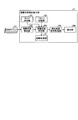
図1は、実施例1に係る情報処理装置の概略構成図である。情報処理装置100は、それぞれ挿抜可能なシステムボード1及び(Input Output)IOボード2を有している。また、システムボード1やIOボード2を情報処理装置100に挿入することを、情報処理装置100に実装するという場合がある。また、情報処理装置100は、ハードディスク3を有している。
FIG. 1 is a schematic configuration diagram of an information processing apparatus according to the first embodiment. The
システムボード1は、主記憶媒体であるDIMM11及び演算処理部であるCPU12を有している。また、システムボード1は、搭載状態検出表示部10を有している。搭載状態検出表示部10については後で詳細に説明する。
The
CPU12及びDIMM11は、システムボード1に対して着脱可能である。CPU12及びDIMM11は、例えば、情報処理装置100の操作者のシステム設計に基づいて個数や性能などが決められ、操作者により、情報処理装置100へ実装される。
The
IOボード2は、PCIデバイス21を有している。PCIデバイス21は、例えば、ネットワークカードやグラフィックカードなどである。そして、PCIデバイス21は、IOボード2に対して着脱可能である。
The
図2は、実施例1に係るシステムボードの構成図である。本実施例においては、システムボード1は、DIMM11を実装するためのDIMMスロット111を32個有している。図2では、各DIMMスロット111にスロット番号をつけて区別している。図2のDIMMスロット111においてDIMMの後に付加されている番号がスロット番号を表す。32個のDIMMスロット111は、それぞれ#0A0〜#0A3、#0B0〜#0B3、#0C0〜#0C3、#0D0〜#0D3、#1A0〜#1A3、#1B0〜#1B3、#1C0〜#1C3、及び、#1D0〜#1D3のスロット番号を用いて表されている。例えば、図2における一番上のDIMMスロット111のスロット番号は、#1D3である。
FIG. 2 is a configuration diagram of the system board according to the first embodiment. In this embodiment, the
また、システムボード1は、メモリコントローラ(Memory Controller:MC)13を8個有している。図2では、各メモリコントローラ13にもコントローラ番号をつけて区別している。図2のメモリコントローラ13において、MCの後に付加されている番号がコントローラ番号を表す。8個のメモリコントローラ13は、それぞれ#0A〜0D及び#1A〜1Dのコントローラ番号を用いて表されている。例えば、図2における一番上のメモリコントローラ13のコントローラ番号は、#1Dである。
Further, the
さらに、システムボード1は、CPU12を2個有している。図2では、CPU12にもCPU番号をつけて区別している。図2のCPU12において、CPUの後に付加されている番号がCPU番号を表す。本実施例では、CPU#0及び#1が搭載されている。
Furthermore, the
また、システムボード1は、コネクタ14を有している。コネクタ14は、情報処理装置100が有するバスに接続するためのコネクタである。
Further, the
各DIMMスロット111は、4つずつ組となって、それぞれのメモリコントローラ13に接続されている。そして、メモリコントローラ13は、4つずつ組となって、それぞれのCPU12に接続されている。さらに、CPU12は、コネクタ14に繋がっている。
Each
さらに、システムボード1において、搭載状態検出表示部10は、各DIMMスロット111と接続されている。
Further, in the
図3は、実施例1に係る搭載状態検出表示部のブロック図である。搭載状態検出表示部10は、モード決定部101、パターン記憶部102、搭載状態検出部103、搭載状態判定部104、検出結果表示処理部105、表示部106及び起動処理部107を有している。
FIG. 3 is a block diagram of the mounting state detection display unit according to the first embodiment. The mounting state
DIMMスロット111には、操作者によりDIMM11が搭載されている。操作者は、CPU12の搭載数、搭載するDIMM11のタイプ及びDIMM11の動作モードに応じて決まるパターンにしたがって、DIMMスロット111にDIMM11を搭載する。しかし、操作者によりDIMM11が搭載された状態では、操作者のミスによる誤搭載や搭載不足が発生しているおそれがある。
A
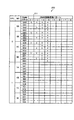
パターン記憶部102は、DIMM搭載モード毎にDIMM搭載候補パターンを記憶している。DIMM搭載モードとは、例えば、CPU12の搭載数、搭載されているDIMM11のタイプ及びDIMM11の動作モードに対応させて決定されたDIMM搭載方法の識別情報である。そして、DIMM搭載候補パターンは、DIMM搭載モード毎に各スロット111に対してDIMM11をどのように配置することができるかを表す情報が登録されている。
The
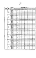
例えば、図4〜11は、パターン記憶部102が記憶するDIMM搭載モード毎のDIMM搭載候補パターンの一例を表している。ここでは、DIMM搭載モードとして8種類のモードが有る場合で説明する。以下の説明では、8種類のDIMM搭載モードに、それぞれ#1〜#9の番号を振って表される。図4は、DIMM搭載モード#1の場合のDIMM搭載候補パターンを示す図である。図5は、DIMM搭載モード#2の場合のDIMM搭載候補パターンを示す図である。図6は、DIMM搭載モード#3の場合のDIMM搭載候補パターンを示す図である。図7は、DIMM搭載モード#4の場合のDIMM搭載候補パターンを示す図である。図8は、DIMM搭載モード#5の場合のDIMM搭載候補パターンを示す図である。図9は、DIMM搭載モード#6の場合のDIMM搭載候補パターンを示す図である。図10は、DIMM搭載モード#7の場合のDIMM搭載候補パターンを示す図である。図11は、DIMM搭載モード#8の場合のDIMM搭載候補パターンを示す図である。すなわち、パターン記憶部102は、DIMM搭載モード#1〜#9のそれぞれに対応させて、図4〜11で表される各DIMM搭載候補パターンを記憶している。
For example, FIGS. 4 to 11 show examples of DIMM installation candidate patterns for each DIMM installation mode stored in the
例えば、図4を例に図4〜9の各図について説明する。DIMM搭載モード#1に対しては、DIMM搭載候補パターン1−1〜1−4で表される4つのパターンが設定されている。また、DIMM搭載モード#1の場合、DIMM搭載候補パターン1−5〜1−8は設定されていない。例えば、図4のテーブル210における列211において、DIMM搭載候補パターン1−1におけるDIMM11のDIMMスロット111への搭載方法が表される。列211の各欄においてチェックが付いている欄が、DIMM11が搭載されるDIMMスロット111を表している。すなわち、DIMM搭載候補パターン1−1では、DIMM#0A0、DIMM#0B0、DIMMスロット#0C0及びDIMMスロット#0D0がDIMM11を搭載するスロットである。
For example, FIGS. 4 to 9 will be described with reference to FIG. 4 as an example. For the DIMM mounting
また、図5〜9で示されるように、各DIMM搭載モードに対応するテーブル220〜280ついても同様に、複数のDIMM搭載候補パターンが登録されている。 Also, as shown in FIGS. 5 to 9, a plurality of DIMM mounting candidate patterns are registered in the same manner for the tables 220 to 280 corresponding to each DIMM mounting mode.
図3に戻って説明を続ける。モード決定部101は、例えば、図12に示すモード決定テーブル200を記憶している。図12は、モード決定テーブルの一例の図である。モード決定テーブル200には、搭載CPU数201、搭載DIMMタイプ202及びDIMM動作モード203の組合せに対応させてDIMM搭載モード204が登録されている。例えば、搭載CPU数201が1の場合、図2におけるCPU#1が搭載されている。また、搭載DIMMタイプ202は、搭載されているDIMM11がバッファを有するRegistered (Buffered) DIMM(RDIMM)であるかバッファを有さないUnbuffered DIMM(UDIMM)であるかを表す。また、DIMM動作モード203は、DIMM11の動作モードが冗長性を有するNon Mirrorであるか冗長性を有さないMirrorであるかを表す。
Returning to FIG. 3, the description will be continued. The
モード決定部101は、情報処理装置100におけるCPU12の搭載数、搭載されているDIMM11のタイプ及びDIMM11の動作モードの入力を操作者から受ける。そして、モード決定部101は、受信したCPU12の搭載数、搭載されているDIMM11のタイプ及びDIMM11の動作モードに対応するDIMM搭載モード204をモード決定テーブル200から決定する。その後、モード決定部101は、決定したDIMM搭載モード204を搭載状態判定部104へ出力する。
The
搭載状態検出部103は、どのDMMスロット111にDIMM11が搭載されているかを検出する。例えば、本実施例では、搭載状態検出部103は、図13に示すような回路を用いてDIMM11の搭載状態を検出する。図13は、DIMM搭載検出回路の一例を示す図である。
The mounting
DIMMスロット111は、端子112及び端子113を有している。DIMM11が挿入されていない場合、点線で表す部分がはずされており、端子112と端子113とは繋がっていない。そして、DIMM11がDIMMスロット111に挿入されると、点線であらわすように端子112と端子113とが接続される。DIMM11は、端子112と端子113との間に内部抵抗114を有する。
The
搭載状態検出部103は、DIMM搭載検出回路131を有している。DIMM搭載検出回路131は、DIMM11の端子112側に電源電圧に接続されるプルアップ抵抗132を有している。また、DIMM搭載検出回路131は、DIMM11の端子113をグランド(Ground:GND)に接続する。
The mounting
端子112と端子113とは接続されていない場合、DIMM搭載検出回路131は、プルアップ抵抗132により電圧が上げられた信号、すなわち論理が「High」の信号を搭載状態判定部104へ出力する。言い換えれば、DIMMスロット111にDIMM11が挿入されていない場合、DIMM搭載検出回路131は、「High」の信号を出力する。
When the terminal 112 and the terminal 113 are not connected, the DIMM mounting
また、端子112と端子113とは接続されている場合、電圧はグランドに落ちるので、DIMM搭載検出回路131は、論理が「Low」の信号を搭載状態判定部104へ出力する。言い換えれば、DIMMスロット111にDIMM11が挿入されている場合、DIMM搭載検出回路131は、「Low」の信号を出力する。
When the terminal 112 and the terminal 113 are connected, the voltage drops to the ground, so the DIMM mounting
図14は、DIMM搭載検出回路が出力する信号の論理表の図である。DIMM搭載検出回路131が出力する信号は、DIMMスロット111にDIMM11が搭載されている場合、「High」となり、DIMMスロット111にDIMM11が搭載されていない場合、「Low」となる。
FIG. 14 is a logical table of signals output from the DIMM mounting detection circuit. The signal output from the DIMM mounting
図14では、スロット番号が#1D3のDIMMスロット111を例に記載しているが、搭載状態検出部103は、他のスロット番号のDIMMスロット111に対してもDIMM搭載検出回路131を有している。
In FIG. 14, the
すなわち、DIMM搭載検出回路131は、32個のDIMMスロット111それぞれについて、DIMM11が搭載されている場合には「Low」の信号を、DIMM11が搭載されていない場合には「High」の信号を搭載状態判定部104へ出力する。ここで、「Low」の信号を「0」と表し「High」の信号を「1」と表すと、DIMM搭載検出回路131は、DIMM11の搭載状態の検出結果として1又は0が32個並んだビット列のパターンを出力する。例えば、DIMM搭載検出回路131は、「011101110111・・・0111」といったパターンを搭載状態判定部104へ出力する。
That is, for each of the 32
搭載状態判定部104は、決定されたDIMM搭載モードの情報の入力をモード決定部101から受ける。そして、搭載状態判定部104は、決定されたDIMM搭載モードに対応するDIMM搭載候補パターンをパターン記憶部102から取得する。
The mounting
また、搭載状態判定部104は、DIMM11の搭載状態の検出結果の入力を搭載状態検出部103から受ける。そして、搭載状態判定部104は、受信した搭載状態の検出結果と取得したDIMM搭載候補パターンとを比較してパターンが一致しているか否かを判定する。一致している場合には、搭載状態判定部104は、パターン一致検出信号を検出結果表示処理部105へ出力する。また、搭載状態判定部104は、システム起動許可信号を起動処理部107へ出力する。
The mounting
これに対して、受信した搭載状態の検出結果と取得したDIMM搭載候補パターンとが一致していない場合には、搭載状態判定部104は、誤搭載又は搭載不足が発生しているDIMMスロット111を検出する。そして、搭載状態判定部104は、誤搭載又は搭載不足が発生しているDIMMスロット111の情報を検出結果表示処理部105へ出力する。
On the other hand, if the received mounting status detection result does not match the acquired DIMM mounting candidate pattern, the mounting
図15は、搭載状態判定部の回路構成の一例を示す図である。本実施例では、搭載状態判定部104は、比較器141、AND回路142〜145を有している。
FIG. 15 is a diagram illustrating an example of a circuit configuration of the mounting state determination unit. In the present embodiment, the mounting
比較器141は、DIMM搭載候補パターン信号及びDIMM搭載状態の検出結果のパターンを表すDIMM搭載状態検出結果パターン信号の入力を受ける。DIMM候補パターン信号は、例えば、図4〜11で表される各候補パターンにおいてDIMM11が搭載されるDIMMスロット111を「1」とし、DIMMが搭載されないDIMMスロット111を「0」として並べた32個のビット列のパターンである。DIMM搭載候補パターン信号は、モード決定部101により決定されたDIMM搭載モードに対応するパターン記憶部102に格納されているDIMM搭載候補パターンが順番に入力される。
The comparator 141 receives a DIMM mounting candidate pattern signal and a DIMM mounting state detection result pattern signal representing a pattern of the detection result of the DIMM mounting state. The DIMM candidate pattern signals are, for example, 32 in which the
比較器141は、DIMM搭載候補パターン信号とDIMM搭載状態検出結果パターン信号とが一致していればHighを出力する。また、比較器141は、DIMM搭載候補パターン信号とDIMM搭載状態検出結果パターン信号とが一致していない場合、Lowを出力する。比較器141からの出力は、検出結果表示処理部105並びにAND回路144及び145へ入力される。
The comparator 141 outputs High if the DIMM mounting candidate pattern signal matches the DIMM mounting state detection result pattern signal. The comparator 141 outputs Low when the DIMM mounting candidate pattern signal does not match the DIMM mounting state detection result pattern signal. The output from the comparator 141 is input to the detection result
AND回路142は、DIMM搭載候補パターン信号の論理を反転させた信号及びDIMM搭載状態検出結果パターン信号の入力を受ける。そして、AND回路142は、受信した信号がいずれもHighの場合にHighの信号を出力する。それ以外の場合、AND回路142は、Lowの信号を出力する。すなわち、DIMM搭載候補パターンとしてはDIMM11を搭載しないDIMMスロット111に、実際にはDIMM11が搭載されている場合に、AND回路142は、Highを出力する。言い換えれば、AND回路142は、誤搭載を検出した場合にHighを出力する。
The AND
AND回路143は、DIMM搭載候補パターン信号及びDIMM搭載状態検出結果パターン信号の論理を反転させた信号の入力を受ける。そして、AND回路143は、受信した信号がいずれもHighの場合にHighの信号を出力する。それ以外の場合、AND回路142は、Lowの信号を出力する。すなわち、DIMM搭載候補パターンとしてはDIMM11を搭載するDIMMスロット111に、実際にはDIMM11が搭載されていない場合に、AND回路143は、Highを出力する。言い換えれば、AND回路143は、搭載不足を検出した場合にHighを出力する。
The AND
AND回路144は、比較器141から出力された信号の論理を反転させた信号及びAND回路142から出力された信号の入力を受ける。そして、AND回路144は、比較器141からの出力がHighの場合、AND回路142から出力されたHighの信号を検出結果表示処理部105へ出力する。すなわち、AND回路145は、DIMM搭載候補パターン信号とDIMM搭載状態検出結果パターン信号とが不一致の場合にHighとなるDIMM誤搭載検出信号を検出結果表示処理部105へ出力する。このDIMM誤搭載検出信号は、0又は1が32個並んだビット列のパターンとなる。
The AND
AND回路145は、比較器141から出力された信号の論理を反転させた信号及びAND回路143から出力された信号の入力を受ける。そして、AND回路145は、比較器141からの出力がHighの場合、AND回路142から出力されたHighの信号を検出結果表示処理部105へ出力する。すなわち、AND回路145は、DIMM搭載候補パターン信号とDIMM搭載状態検出結果パターン信号とが不一致の場合に、HighとなるDIMM搭載不足検出信号を検出結果表示処理部105へ出力する。このDIMM搭載不足検出信号も、0又は1が32個並んだビット列のパターンとなる。
The AND
この搭載状態判定部104が、「異常検出部」の一例にあたる。
The mounting
検出結果表示処理部105は、DIMM搭載候補パターン信号及びDIMM搭載状態検出結果パターン信号のパターンが一致した場合、パターン一致検出信号の入力を搭載状態判定部104から受ける。例えば、検出結果表示処理部105は、あるDIMM搭載候補パターンを用いての比較を開始してから32個のHighの信号が連続して入力された場合に、DIMM搭載候補パターンが入力されたと判定しても良い。
The detection result
また、DIMM搭載候補パターン信号及びDIMM搭載状態検出結果パターン信号のパターンが一致しない場合、検出結果表示処理部105は、誤搭載又は搭載不足のDIMMスロット111を表す信号のいずれかもしくは双方の入力を搭載状態判定部104から受ける。検出結果表示処理部105は、DIMM搭載候補パターン毎に、誤搭載及び搭載不足のDIMMスロット111を表す信号の入力を受けていく。
If the patterns of the DIMM mounting candidate pattern signal and the DIMM mounting state detection result pattern signal do not match, the detection result
各DIMM搭載候補パターンについての誤搭載又は搭載不足の情報を受信した後、パターン一致検出信号の入力を受けた場合、検出結果表示処理部105は、それ以前に比較したDIMM搭載候補パターンにおける誤搭載及び搭載不足の情報を消去する。
When receiving the input of the pattern match detection signal after receiving the information of erroneous mounting or insufficient mounting for each DIMM mounting candidate pattern, the detection result
一方、全てのDIMM搭載候補パターンにおいてパターン一致検出信号を受信しない場合、検出結果表示処理部105は、不一致箇所の合計数が最も少ないDIMM搭載候補パターンを特定する。そして、検出結果表示処理部105は、特定したDIMM搭載候補パターンにおける誤搭載又は搭載不足のDIMMスロット111を示す情報を表示部106に表示させる。
On the other hand, when the pattern match detection signal is not received in all the DIMM mounting candidate patterns, the detection result
図16は、検出結果表示処理部の回路構成の一例を示す図である。本実施例では、検出結果表示処理部105は、比較器151、スイッチ152及び153、並びに、AND回路154及び155を有している。図16では、パターンが不一致の場合に不一致のDIMMスロット111を表示するための回路構成を示している。実際には、パターンが一致した場合には、検出結果表示処理部105は、表示をクリアする。以下では、パターンが一致しない場合の動作について説明する。
FIG. 16 is a diagram illustrating an example of a circuit configuration of the detection result display processing unit. In the present embodiment, the detection result
比較器151は、最初に比較したDIMM搭載候補パターンを表示候補とする。
The
そして、比較器151は、表示候補としているDIMM搭載候補パターンにおけるパターン不一致箇所の合計数及び今回比較しているDIMM搭載候補パターンにおけるパターン不一致箇所の今回合計数の入力を受ける。ここで、今回合計数が表示候補の不一致箇所の合計数より多い場合、比較器151は、Highの信号をスイッチ152及びスイッチ153へ入力する。そして、比較器151は、今回比較に用いたDIMM搭載候補パターンを次の表示候補とする。
Then, the
これに対して、今回合計数が表示候補の不一致箇所の合計数以下の場合、比較器151は、Lowの信号をスイッチ152及びスイッチ153へ入力する。
On the other hand, when the current total number is equal to or smaller than the total number of mismatched portions of display candidates, the
スイッチ152は、DIMM誤搭載検出信号の入力を搭載状態判定部104から受ける。そして、スイッチ152は、Highの信号を比較器151から受けた場合、搭載状態判定部104から受信したDIMM誤搭載検出信号をAND回路154へ出力する。これに対して、Lowの信号を比較器151から受けた場合、スイッチ152は、Lowの信号をAND回路154へ出力する。
The
スイッチ153は、DIMM搭載不足検出信号の入力を搭載状態判定部104から受ける。そして、スイッチ153は、Highの信号を比較器151から受けた場合、搭載状態判定部104から受信したDIMM搭載不足検出信号をAND回路155へ出力する。これに対して、Lowの信号を比較器151から受けた場合、スイッチ153は、Lowの信号をAND回路155へ出力する。
The
AND回路154は、パターン一致検出信号の論理を反転させた信号の入力を搭載状態判定部104から受ける。また、AND回路154は、今回比較に用いたパターンの不一致箇所の合計数が表示候補の不一致箇所の合計数より少ない場合、搭載状態判定部104が出力したDIMM誤搭載検出信号の入力を受ける。そして、パターン一致検出信号がLowの場合、すなわち今回のDIMM搭載候補パターンが実際のDIMM11の搭載状態と一致していない場合、AND回路154は、DIMM誤搭載検出信号と同じビット列のパターンを有するDIMM誤搭載表示信号を表示部106へ出力する。ここで、DIMM誤搭載表示信号は、0又は1が32個並んだビット列のパターンとなる。そして、DIMM誤搭載表示信号における「1」が誤搭載のDIMMスロット111を表している。
The AND
AND回路155は、パターン一致検出信号の論理を反転させた信号の入力を搭載状態判定部104から受ける。また、AND回路155は、今回比較に用いたパターンの不一致箇所の合計数が表示候補の不一致箇所の合計数より少ない場合、搭載状態判定部104が出力したDIMM搭載不足検出信号の入力を受ける。そして、パターン一致検出信号がLowの場合、すなわち今回のDIMM搭載候補パターンが実際のDIMM11の搭載状態と一致していない場合、AND回路155は、DIMM搭載不足検出信号と同じビット列のパターンを有するDIMM搭載不足表示信号を表示部106へ出力する。ここで、DIMM搭載不足表示信号は、0又は1が32個並んだビット列のパターンとなる。そして、DIMM搭載不足表示信号における「1」が搭載不足のDIMMスロット111を表している。この検出結果表示処理部105が、「報知部」の一例にあたる。
The AND
表示部106は、DIMM誤搭載表示信号及びDIMM搭載不足表示信号の入力を検出結果表示処理部105から受ける。そして、表示部106は、DIMM誤搭載表示信号によって示される誤搭載のDIMMスロット111の情報を表示する。また、表示部106は、DIMM搭載不足表示信号によって示される搭載不足のDIMMスロット111の情報を表示する。以下に、表示部106による誤搭載及び搭載不足のDIMMスロット111の表示方法の一例について説明する。
The
本実施例では、表示部106は、図17に示す誤搭載表示Light Emitting Diode(LED)15及び搭載不足表示LED16を有する。図17は、表示部の一例を説明するための図である。図17に示すように、誤搭載表示LED15及び搭載不足表示LED16は、各DIMMスロット111に対応するようにそれぞれ32個ずつシステムボード1上に配置されている。
In the present embodiment, the
誤搭載表示LED15は、例えば、図16のAND回路154の出力端子に接続されている。そして、誤搭載表示LED15は、AND回路154から出力されたビット列のパターンを受信する。図17の最下部の誤搭載表示LED15から順に、受信したパターンの先頭から1ビットずつが入力されていく。そして、入力値が「1」の誤搭載表示LED15は点灯し、入力値が「0」の誤搭載表示LED15は消灯する。操作者は、点灯している誤搭載表示LED15に対応するDIMMスロット111に間違ってDIMM11が搭載されていることが分かる。例えば、図17の状態であれば、操作者は、スロット番号が#1C2のDIMMスロット111に間違ってDIMM11が搭載されていることが把握できる。
The erroneous
搭載不足表示LED16は、例えば、図16のAND回路155の出力端子に接続されている。そして、搭載不足表示LED16は、AND回路155から出力されたビット列のパターンを受信する。図17の最下部の搭載不足表示LED16から順に、受信したパターンの先頭から1ビットずつが入力されていく。そして、入力値が「1」の搭載不足表示LED16は点灯し、入力値が「0」の搭載不足表示LED16は消灯する。操作者は、点灯している搭載不足表示LED16に対応するDIMMスロット111にDIMM11が搭載されていないことが分かる。例えば、図17の状態であれば、操作者は、スロット番号が#0A0のDIMMスロット111にDIMM11が搭載されていないことが把握できる。
The
ここで、表示部106としてLEDを用いて誤搭載及び搭載不足のDIMMスロット111の情報の表示を行ったが、操作者が誤搭載及び搭載不足のDIMMスロット111を特定できれば表示方法は特に制限は無い。例えば、表示部16をモニタとして、モニタに誤搭載及び搭載不足のDIMMスロット111の情報を表示してもよい。
Here, the information of the erroneously installed and insufficiently
図3に戻って説明を続ける。起動処理部106は、DIMM11がDIMM搭載候補パターンにしたがって搭載されている場合、システム起動許可信号を搭載状態判定部104から受信する。そして、起動処理部107は、情報処理装置100のシステムを起動させる。これに対して、DIMM11がDIMM搭載候補パターンにしたがって搭載されていなければ、システム起動許可信号を受信しないので、起動処理部107は、システムの起動を開始しない。起動処理部107の機能は、CPU12によって実現される。
Returning to FIG. 3, the description will be continued. The
次に、図18を参照して、本実施例に係る情報処理装置100によるDIMM11の誤搭載及び搭載不足の判定処理の全体的な流れについて説明する。図18は、実施例1に係る情報処理装置によるDIMMの誤搭載及び搭載不足の判定処理のフローチャートである。
Next, with reference to FIG. 18, an overall flow of the processing for determining whether the
操作者は、DIMM11をDIMMスロット111へ搭載する(ステップS1)。
The operator installs the
さらに、DIMM11が搭載されたシステムボード1を情報処理装置100の筐体に実装し、システムボード1へ通電する(ステップS2)。
Further, the
情報処理装置100は、DIMM11のDIMMスロット111への誤搭載又は搭載不足が発生していないか否かを判定する(ステップS3)。誤搭載又は搭載不足が発生している場合(ステップS3:肯定)、情報処理装置100は、搭載異常を検出する(ステップS4)。
The
そして、情報処理装置100は、誤搭載及び搭載不足のDIMMスロット111の検出結果を表示する(ステップS5)。
Then, the
操作者は、誤搭載及び搭載不足のDIMMスロット111の検出結果の表示を確認して、DIMM11を再搭載する(ステップS6)。その後、情報処理装置100は、ステップS2へ戻る。
The operator confirms the display of the detection result of the erroneously installed and insufficiently
これに対して、誤搭載及び搭載不足のいずれも発生していない場合、すなわち、DIMM11がDIMM搭載候補パターンにしたがって適切に搭載されている場合(ステップS3:否定)、情報処理装置100は、システムの起動を開始する(ステップS7)。
On the other hand, if neither erroneous mounting nor insufficient mounting occurs, that is, if the
次に、情報処理装置100は、SPD専用プログラムを起動する(ステップS8)。
Next, the
そして、情報処理装置100は、起動したSPD専用プログラムを用いて、DIMM11からSPDを読み出す(ステップS9)。
Then, the
次に、情報処理装置100は、POSTを実行する(ステップS10)。
Next, the
POSTでエラーが検出されなければ、情報処理装置100は、Operating System(OS)をブートさせる(ステップS11)。
If no error is detected by POST, the
そして、情報処理装置100は、システムの起動を完了する(ステップS12)。
Then, the
次に、図19を参照して、搭載状態判定部104によるDIMM11の搭載状態判定処理の流れについて説明する。図19は、搭載状態判定部によるDIMMの搭載状態判定処理のフローチャートである。図19のフローは、図18のステップS3における処理にあたる。
Next, with reference to FIG. 19, the flow of the mounting state determination process of the
搭載状態判定部104は、DIMM搭載モードの情報をモード決定部101から取得する(ステップS101)。
The mounting
次に、搭載状態判定部104は、取得したDIMM搭載モードに対応するDIMM搭載候補パターンをパターン記憶部102が記憶しているDIMM搭載候補パターンの中から特定する(ステップS102)。
Next, the mounting
搭載状態判定部104は、特定したDIMM搭載候補パターンからDIMM搭載判定未処理のパターンを1つ選択する(ステップS103)。
The mounting
そして、搭載状態判定部104は、選択したDIMM搭載候補パターンと実際のDIMM11のDIMMスロット111への搭載状態とが一致しているか否かを判定する(ステップS104)。一致している場合(ステップS104:肯定)、搭載状態判定部104は、パターン一致検出信号を検出結果表示処理部105へ出力する(ステップS105)。
Then, the mounting
さらに、搭載状態判定部104は、システム起動許可信号を起動処理部107へ発行する(ステップS106)。そして、搭載状態判定部104は、搭載状態判定処理を終了する。
Further, the mounting
一方、不一致の場合(ステップS104:否定)、搭載状態判定部104は、選択したDIMM搭載候補パターンにおける搭載位置でないDIMMスロット111へのDIMM11の搭載があるか否かを判定する(ステップS107)。誤搭載が無い場合(ステップS107:否定)、搭載状態判定部104は、ステップS109へ進む。
On the other hand, if they do not match (No at Step S104), the mounting
これに対して、誤搭載がある場合(ステップS107:肯定)、搭載状態判定部104は、該当するDIMMスロット111毎に誤搭載検出信号を出力する(ステップS108)。
On the other hand, if there is an incorrect mounting (step S107: Yes), the mounting
次に、搭載状態判定部104は、選択したDIMM搭載候補パターンにおける搭載位置のDIMMスロット111へのDIMM11の未搭載があるか否かを判定する(ステップS109)。未搭載のDIMMスロット111が無い場合(ステップS109:否定)、搭載状態判定部104は、ステップS111へ進む。
Next, the mounting
これに対して、未搭載のDIMMスロット111が無い場合(ステップS109:否定)、搭載状態判定部104は、ステップS111へ進む。
On the other hand, if there is no unmounted DIMM slot 111 (No at Step S109), the mounting
一方、未搭載のDIMMスロット111がある場合(ステップS109:肯定)、搭載状態判定部104は、該当するDIMMスロット111毎に搭載不足検出信号を出力する(ステップS110)。
On the other hand, when there is an unmounted DIMM slot 111 (step S109: Yes), the mounting
その後、搭載状態判定部104は、判定未処理のDIMM搭載候補パターンがあるか否かを判定する(ステップS111)。判定未処理のDIMM搭載候補パターンがある場合(ステップS111:肯定)、搭載状態判定部104は、ステップS103へ進む。
Thereafter, the mounting
一方、判定未処理のDIMM搭載候補パターンが無い場合(ステップS111:否定)、搭載状態判定部104は、搭載状態判定処理を終了する。
On the other hand, if there is no unprocessed DIMM mounting candidate pattern (No at Step S111), the mounting
次に、図20を参照して、検出結果表示処理部105による検出結果判定処理の流れについて説明する。図20は、実施例1に係る検出結果表示処理部による検出結果表示処理のフローチャートである。図20のフローは、図18のステップS5における処理にあたる。
Next, the flow of detection result determination processing by the detection result
検出結果表示処理部105は、パターン一致検出信号を受信したか否かを判定する(ステップS201)。パターン一致検出信号を受信した場合(ステップS201:肯定)、検出結果表示処理部105は、全ての誤搭載検出結果と搭載不足検出結果をクリアする(ステップS202)。そして、検出結果表示処理部105は、検出結果表示処理を終了する。
The detection result
これに対して、パターン一致検出信号を受信していない場合(ステップS201:否定)、検出結果表示処理部105は、今回のDIMM搭載候補パターンと実際のDIMM11の搭載状態との不一致箇所の合計数である今回候補合計数を算出する(ステップS203)。
On the other hand, if the pattern match detection signal has not been received (No at Step S201), the detection result
そして、検出結果表示処理部105は、今回合計数が表示候補となっているDIMM搭載候補パターンと実際のDIMM11の搭載状態との不一致箇所の合計数である表示候補合計数未満か否かを判定する(ステップS204)。今回合計数が表示候補合計数以上の場合(ステップS204:否定)、検出結果表示処理部105は、ステップS207へ進む。
Then, the detection result
これに対して、今回合計数が表示候補合計数未満の場合(ステップS204:肯定)、検出結果表示処理部105は、現在のDIMM11の搭載状態と今回のDIMM搭載候補パターンとの比較結果をDIMMの誤搭載検出結果と未搭載検出結果として反映し(ステップS205)、表示部106に表示させる。ただし、今回のDIMM搭載候補パターンが最初のDIMM搭載候補パターンの場合、検出結果表示処理部105は、比較が行えないので、そのままステップS205へ進む。
On the other hand, when the current total number is less than the display candidate total number (step S204: affirmative), the detection result
そして、検出結果表示処理部105は、今回のDIMM搭載候補パターンを表示候補とする(ステップS206)。
Then, the detection result
検出結果表示処理部105は、表示判定が未処理のDIMM搭載候補パターンがあるか否かを判定する(ステップS207)。未処理のDIMM搭載候補パターンがある場合(ステップS207:肯定)、検出結果表示処理部105は、ステップS201へ戻る。
The detection result
これに対して、未処理のDIMM搭載候補パターンが無い場合(ステップS207:否定)、検出結果表示処理部105は、検出結果表示処理を終了する。
On the other hand, when there is no unprocessed DIMM mounting candidate pattern (No at Step S207), the detection result
以上に説明したように、本実施例に係る情報処理装置は、システムの起動前にDIMMの誤搭載及び搭載不足を検出し、検出結果を表示して操作者に通知する。これにより、操作者は、早期にDIMMの誤搭載及び搭載不足を発見でき、DIMMの誤搭載及び搭載不足によるシステムの停止及び再起動の発生を回避することができる。この結果、システムの構築、並びに、メモリの運用及び保守といった装置の正常起動までの操作者の工数負担を軽減することができる。 As described above, the information processing apparatus according to the present embodiment detects an erroneous mounting or insufficient mounting of a DIMM before starting the system, displays the detection result, and notifies the operator. As a result, the operator can discover a DIMM misloading and mounting shortage at an early stage, and can prevent the system from being stopped and restarted due to a DIMM misloading and mounting shortage. As a result, it is possible to reduce the man-hour burden on the operator until normal startup of the apparatus such as system construction and memory operation and maintenance.
次に、実施例2について説明する。本実施例に係る情報処理装置は、DIMMの誤搭載及び搭載不足の検出結果の表示に用いるDIMM搭載候補パターンの選択方法が実施例1と異なる。本実施例に係る情報処理装置における各部も図3のブロック図で表される。以下の説明では、実施例1と同じ機能を有する各部については説明を省略する。 Next, Example 2 will be described. The information processing apparatus according to the present embodiment is different from the first embodiment in a method for selecting a DIMM mounting candidate pattern used for displaying a detection result of a DIMM erroneous mounting and mounting shortage. Each part in the information processing apparatus according to the present embodiment is also represented by the block diagram of FIG. In the following description, description of each part having the same function as in the first embodiment is omitted.
図21を参照して、本実施例に係る検出結果表示処理部105による検出結果判定処理について説明する。図21は、実施例2に係る検出結果表示処理部による検出結果表示処理のフローチャートである。
With reference to FIG. 21, the detection result determination process by the detection result
検出結果表示処理部105は、パターン一致検出信号を受信したか否かを判定する(ステップS301)。パターン一致検出信号を受信した場合(ステップS301:肯定)、検出結果表示処理部105は、全ての誤搭載検出結果と搭載不足検出結果をクリアする(ステップS302)。そして、検出結果表示処理部105は、検出結果表示処理を終了する。
The detection result
これに対して、パターン一致検出信号を受信していない場合(ステップS301:否定)、検出結果表示処理部105は、今回のDIMM搭載候補パターンのDIMM搭載個数と実際のDIMM11の搭載個数との差である今回差分を算出する(ステップS303)。
On the other hand, when the pattern coincidence detection signal is not received (No at Step S301), the detection result
そして、検出結果表示処理部105は、今回差分が表示候補となっているDIMM搭載候補パターンのDIMM搭載個数と実際のDIMM11の搭載個数との差分である表示候補差分未満か否かを判定する(ステップS304)。今回差分が表示候補差分以上の場合(ステップS304:否定)、検出結果表示処理部105は、ステップS306へ進む。
Then, the detection result
これに対して、今回差分が表示候補差分未満の場合(ステップS304:肯定)、検出結果表示処理部105は、現在のDIMM11の搭載状態と今回のDIMM搭載候補パターンとの比較結果をDIMMの誤搭載検出結果と未搭載検出結果として反映し(ステップS305)、表示部106に表示させる。ただし、今回のDIMM搭載候補パターンが最初のDIMM搭載候補パターンの場合、検出結果表示処理部105は、比較が行えないので、そのままステップS305へ進む。
In contrast, when the current difference is less than the display candidate difference (step S304: affirmative), the detection result
そして、検出結果表示処理部105は、今回のDIMM搭載候補パターンを表示候補とする(ステップS306)。
Then, the detection result
検出結果表示処理部105は、表示判定が未処理のDIMM搭載候補パターンがあるか否かを判定する(ステップS307)。未処理のDIMM搭載候補パターンがある場合(ステップS307:肯定)、検出結果表示処理部105は、ステップS301へ戻る。
The detection result
これに対して、未処理のDIMM搭載候補パターンが無い場合(ステップS307:否定)、検出結果表示処理部105は、検出結果表示処理を終了する。
On the other hand, when there is no unprocessed DIMM mounting candidate pattern (step S307: No), the detection result
以上に説明したように、本実施例に係る情報処理装置は、実際のDIMMの搭載状態とのDIMM搭載数の差が最小となるDIMM搭載候補パターンとの比較結果を表示して、DIMMの誤搭載及び搭載不足を通知する。 As described above, the information processing apparatus according to the present embodiment displays the comparison result with the DIMM installation candidate pattern that minimizes the difference in the number of installed DIMMs from the actual DIMM installation state, and displays a DIMM error. Notify loading and unloading.
このように、誤搭載及び搭載不足の検出及び表示における比較対象とするDIMM搭載候補パターンの選択は、様々な方法で実現することができる。そして、実施例2のような選択方法を用いても、DIMMの誤搭載及び搭載不足を操作者に適切に通知することができる。 As described above, selection of a DIMM mounting candidate pattern to be compared in detection and display of erroneous mounting and mounting shortage can be realized by various methods. Even if the selection method as in the second embodiment is used, it is possible to appropriately notify the operator of DIMM mismounting and insufficient mounting.
次に、実施例3について説明する。本実施例に係る搭載状態検出表示部10のブロック図も図3で表される。本実施例では、実施例1ではハードウェア回路として実現した搭載状態判定部104及び検出結果表示処理部105をMulti Processing Unit(MPU)により実現する。
Next, Example 3 will be described. A block diagram of the mounting state
図22は、実施例3に係るシステムボードの構成図である。本実施例に係るシステムボード1は、DIMMスロット111、CPU12、メモリコントローラ13、コネクタ14、搭載状態検出部103及びMPU18を有する。
FIG. 22 is a configuration diagram of a system board according to the third embodiment. The
搭載状態検出部103は、実施例1と同様に図13で表される構成を有している。
The mounting
MPU18は、搭載状態判定部104及び検出結果表示処理部105の機能を実現するプログラムを含む各種プログラムを記憶している。そして、MPU18は、記憶する各種プログラムを実行することで、搭載状態判定部104及び検出結果表示処理部105の機能を実現する。
The
例えば、MPU18は、各DIMMスロット111に対するDIMM11の搭載状態の検出結果の入力を搭載状態検出部103から受ける。
For example, the
そして、MPU18は各種プログラムを実行することで、モード決定部101からDIMM搭載モードを受信し、受信したDIMM搭載モードに対応するDIMM搭載候補パターンをパターン記憶部102から取得する機能を実現する。
The
そして、MPU18は各種プログラムを実行することで、DIMM搭載候補パターンとDIMM11の搭載状態の検出結果からDIMM11の誤搭載及び搭載不足を検出し表示部106へ表示させる機能を実現する。
Then, the
また、本実施例では、MPU18がプログラムを実行して搭載状態判定部104及び検出結果表示処理部105の機能を実現する場合で説明したが、プログラムの実行はMPUに限らず、例えばField Programmable Gate Array(FPGA)などでもよい。
In the present embodiment, the
このように、搭載状態検出部103及びMPU18によって、搭載状態検出表示部10の機能が実現される。
Thus, the function of the mounting state
以上に説明したように、本実施例に係る情報処理装置は、所定のプログラムを実行することで搭載状態判定部及び検出結果表示処理部の機能を実現する。このように、プログラムの実行により機能を実現した場合、運用に合わせて細かい処理を設定することができ、検出及び表示処理の方法を適切に選択することができる。 As described above, the information processing apparatus according to the present embodiment realizes the functions of the mounting state determination unit and the detection result display processing unit by executing a predetermined program. As described above, when the function is realized by executing the program, fine processing can be set in accordance with the operation, and a detection and display processing method can be appropriately selected.
次に、実施例4について説明する。本実施例に係る情報処理装置は、Peripheral Component Interconnect(PCI)デバイスの誤搭載及び搭載不足を検出することが実施例1と異なる。 Next, Example 4 will be described. The information processing apparatus according to the present embodiment is different from the first embodiment in that it detects erroneous mounting and insufficient mounting of a peripheral component interconnect (PCI) device.
図23は、実施例4に係るIOボードの構成図である。本実施例に係るIOボード2は、搭載状態検出表示部20、PCIスロット311、PCIスイッチ22及びPCIスイッチ23を有している。
FIG. 23 is a configuration diagram of an IO board according to the fourth embodiment. The
PICスロット311にはPCIデバイス21が搭載される。PCIスイッチ22は、PCIスロット311に接続している1段目のPCIスイッチである。また、PCIスイッチ23は、PCIスロット311に接続し、コネクタ24との間でデータの送受信を行う2段目のPCIスイッチである。
The
本実施例に係る搭載状態検出表示部20は、図24に示すブロック図で表される。図24は、実施例4に係る搭載状態検出表示部のブロック図である。図24の各部は、図3に示す各部のDIMMに対する各機能をPCIに置き換えた機能を有している。
The mounting state
モード決定部301は、図25に示すPCIモード決定テーブル310を記憶している。図25は、PCIモード決定テーブルの一例を表す図である。PCIモード決定テーブル310は、搭載PCIスイッチ数、搭載PCIタイプ及びPCI動作モードの組に対応させてPCI搭載モードの情報を格納している。
The
搭載PCIスイッチ数は、2段目のPCIスイッチ23の搭載個数である。搭載PCIタイプは、搭載されているPCIデバイス21の規格である。Gen(Generation)2は、規格PCI Express 2.0を表している。また、Gen3は、規格PCI Express 3.0を表している。PCI動作モードは、例えば、バスモード及びセグメントモードがある。
The number of mounted PCI switches is the number of mounted PCI switches 23 in the second stage. The mounted PCI type is a standard of the mounted
モード決定部301は、情報処理装置100に搭載されているPCIスイッチ23の個数、搭載PCIタイプ及びPCI動作モードの指定を受けて、対応するPCI搭載モードを決定し、搭載状態判定部304へ通知する。
The
パターン記憶部302は、PCI動作モード毎に対応するPCI搭載候補パターンを記憶している。
The
搭載状態検出部303は、PCIスロット311へのPCIの搭載状態を検出する。
The mounting
搭載状態判定部304は、モード決定部301から取得したPCI搭載モードに対応するPCI搭載候補パターンを取得する。そして、搭載状態判定部304は、各PCI搭載候補パターンと現在のPCIデバイス21の搭載状態を比較して、PCI搭載候補パターン毎にPCIデバイス21の誤搭載及び搭載不足を検出する。誤搭載及び搭載不足が無ければ、搭載状態判定部304は、システム起動許可信号を起動処理部307へ出力する。
The mounting
検出結果表示処理部305は、PCI搭載候補パターン毎の誤搭載及び搭載不足の検出結果を搭載状態判定部304から取得する。そして、検出結果表示処理部305は、表示する誤搭載及び搭載不足の検出結果を決定し、表示部306に表示させる。
The detection result
以上に説明したように、本実施例に係る情報処理装置は、PCIデバイスの誤搭載及び搭載不足をシステムの起動前に検出し操作者に通知する。これにより、操作者は、早期にPCIデバイスの誤搭載及び搭載不足を発見でき、迅速に対処することができる。この結果、システムの構築、並びに、PCIデバイスの運用及び保守といった操作者の工数負担を軽減することができる。 As described above, the information processing apparatus according to the present embodiment detects an erroneous mounting and insufficient mounting of a PCI device before starting the system and notifies the operator. As a result, the operator can find out the erroneous mounting and insufficient mounting of the PCI device at an early stage, and can quickly cope with it. As a result, it is possible to reduce the man-hour burden on the operator such as system construction and PCI device operation and maintenance.
また、以上の説明では、DIMMの誤搭載及び搭載不足の検出の場合とPCIデバイスの誤搭載及び搭載不足の検出の場合を分けて説明したが、これらは組み合わせて使用することもできる。 In the above description, the case of detection of erroneous mounting and insufficient mounting of a DIMM is described separately from the case of detection of erroneous mounting and mounting of a PCI device, but these can also be used in combination.
1 システムボード
2 IOボード
3 ハードディスク
10,20 搭載状態検出表示部
11 DIMM
12 CPU
21 PCIデバイス
101,301 モード決定部
102,302 パターン記憶部
103,303 搭載状態検出部
104,304 搭載状態判定部
105,305 検出結果表示処理部
106,306 表示部
107,307 起動処理部
111 DIMMスロット
311 PCIスロットDESCRIPTION OF
12 CPU
21
Claims (8)
各前記スロットにおける前記電子部品の搭載の有無を検出する搭載状態検出部と、
演算処理部の数、前記電子部品の種類及び前記電子部品の動作モードを基に、各前記スロットに対する前記電子部品の搭載の有無を表す搭載候補パターンを決定し、前記搭載状態検出部による検出結果及び前記搭載候補パターンを基に、前記電子部品の搭載異常を検出する異常検出部と、
前記異常検出部により前記搭載異常が検出された場合、前記搭載異常を報知する報知部と
を備えたことを特徴とする情報処理装置。 A plurality of slots for mounting electronic components;
A mounting state detection unit for detecting whether or not the electronic component is mounted in each slot;
Based on the number of arithmetic processing units, the type of the electronic component, and the operation mode of the electronic component, a mounting candidate pattern indicating whether or not the electronic component is mounted in each slot is determined, and the detection result by the mounting state detection unit And based on the mounting candidate pattern, an abnormality detection unit that detects mounting abnormality of the electronic component,
An information processing apparatus comprising: a notifying unit that notifies the mounting abnormality when the abnormality detecting unit detects the mounting abnormality.
前記異常検出部は、自装置の構成を基に、前記記憶部から前記搭載候補パターンを取得する
ことを特徴とする請求項1に記載の情報処理装置。 A storage unit for storing the mounting candidate pattern corresponding to the configuration of the device;
The information processing apparatus according to claim 1, wherein the abnormality detection unit acquires the mounting candidate pattern from the storage unit based on a configuration of the own device.
前記異常検出部は、演算処理部の数、DIMMの種類及びDIMMの動作モードを基に、前記搭載候補パターンを決定することを特徴とする請求項1に記載の情報処理装置。 The electronic component is a DIMM;
The information processing apparatus according to claim 1, wherein the abnormality detection unit determines the mounting candidate pattern based on a number of arithmetic processing units, a DIMM type, and a DIMM operation mode.
演算処理部の数、前記電子部品の種類及び前記電子部品の動作モードを基に、各前記スロットに対する前記電子部品の搭載の有無を表す搭載候補パターンを決定し、
前記電子部品の搭載の有無の検出結果及び前記搭載候補パターンを基に、前記電子部品の搭載異常を検出し、
前記搭載異常を報知する
処理をコンピュータに実行させることを特徴とする情報処理装置制御プログラム。 Detecting presence or absence of mounting of the electronic component in a plurality of slots for mounting the electronic component;
Based on the number of arithmetic processing units, the type of the electronic component, and the operation mode of the electronic component, determine a mounting candidate pattern indicating whether or not the electronic component is mounted on each slot,
Based on the detection result of the presence / absence of mounting of the electronic component and the mounting candidate pattern, the mounting abnormality of the electronic component is detected,
An information processing apparatus control program that causes a computer to execute a process of notifying the mounting abnormality.
Applications Claiming Priority (1)
| Application Number | Priority Date | Filing Date | Title |
|---|---|---|---|
| PCT/JP2013/082404 WO2015083226A1 (en) | 2013-12-02 | 2013-12-02 | Information processing device and information processing device control program |
Publications (2)
| Publication Number | Publication Date |
|---|---|
| JP6094685B2 true JP6094685B2 (en) | 2017-03-15 |
| JPWO2015083226A1 JPWO2015083226A1 (en) | 2017-03-16 |
Family
ID=53273024
Family Applications (1)
| Application Number | Title | Priority Date | Filing Date |
|---|---|---|---|
| JP2015551308A Active JP6094685B2 (en) | 2013-12-02 | 2013-12-02 | Information processing apparatus and information processing apparatus control program |
Country Status (3)
| Country | Link |
|---|---|
| US (1) | US10025683B2 (en) |
| JP (1) | JP6094685B2 (en) |
| WO (1) | WO2015083226A1 (en) |
Families Citing this family (2)
| Publication number | Priority date | Publication date | Assignee | Title |
|---|---|---|---|---|
| TWI622883B (en) * | 2017-04-20 | 2018-05-01 | 遠東金士頓科技股份有限公司 | Control system and control method for controlling memory modules |
| JP7081855B1 (en) * | 2021-05-10 | 2022-06-07 | Necプラットフォームズ株式会社 | Display system, information processing system, display method and program |
Citations (4)
| Publication number | Priority date | Publication date | Assignee | Title |
|---|---|---|---|---|
| JPS61162899A (en) * | 1985-01-11 | 1986-07-23 | Fuji Electric Co Ltd | Device for detecting erroneous insertion of prom |
| JP2003114739A (en) * | 2001-10-09 | 2003-04-18 | Seiko Epson Corp | Main board, substrate for memory module, and memory module |
| US20090157911A1 (en) * | 2007-12-17 | 2009-06-18 | Takashi Aihara | Recording control apparatus, recording control method, and computer program product |
| JP2009169940A (en) * | 2007-12-17 | 2009-07-30 | Ricoh Co Ltd | Recording control apparatus, recording control method, recording control program and storage medium |
Family Cites Families (8)
| Publication number | Priority date | Publication date | Assignee | Title |
|---|---|---|---|---|
| US5922055A (en) * | 1997-02-25 | 1999-07-13 | Motorola, Inc. | Method for determining a type of a serial EEPROM and plug and play controller |
| US6625680B1 (en) * | 1999-08-16 | 2003-09-23 | Cisco Technology, Inc. | System and method for processing circuit card connector and redundancy events |
| JP2002259227A (en) | 2001-03-02 | 2002-09-13 | Ricoh Co Ltd | Electronic apparatus and recording medium recorded with its control program |
| JP2003029998A (en) | 2001-07-19 | 2003-01-31 | Hitachi Ltd | Information processor provided with console displaying operation state of redundant or duplexed logic part |
| US8006028B2 (en) * | 2008-04-08 | 2011-08-23 | International Business Machines Corporation | Enabling memory module slots in a computing system after a repair action |
| CN102081562A (en) * | 2009-11-30 | 2011-06-01 | 华为技术有限公司 | Equipment diagnosis method and system |
| CN102339250A (en) * | 2010-07-16 | 2012-02-01 | 鸿富锦精密工业(深圳)有限公司 | Mainboard signal testing device |
| US8639918B2 (en) * | 2011-08-31 | 2014-01-28 | Dell Products L.P. | Memory compatibility system and method |
-
2013
- 2013-12-02 JP JP2015551308A patent/JP6094685B2/en active Active
- 2013-12-02 WO PCT/JP2013/082404 patent/WO2015083226A1/en active Application Filing
-
2016
- 2016-05-27 US US15/166,327 patent/US10025683B2/en active Active
Patent Citations (4)
| Publication number | Priority date | Publication date | Assignee | Title |
|---|---|---|---|---|
| JPS61162899A (en) * | 1985-01-11 | 1986-07-23 | Fuji Electric Co Ltd | Device for detecting erroneous insertion of prom |
| JP2003114739A (en) * | 2001-10-09 | 2003-04-18 | Seiko Epson Corp | Main board, substrate for memory module, and memory module |
| US20090157911A1 (en) * | 2007-12-17 | 2009-06-18 | Takashi Aihara | Recording control apparatus, recording control method, and computer program product |
| JP2009169940A (en) * | 2007-12-17 | 2009-07-30 | Ricoh Co Ltd | Recording control apparatus, recording control method, recording control program and storage medium |
Also Published As
| Publication number | Publication date |
|---|---|
| JPWO2015083226A1 (en) | 2017-03-16 |
| WO2015083226A1 (en) | 2015-06-11 |
| US10025683B2 (en) | 2018-07-17 |
| US20160274984A1 (en) | 2016-09-22 |
Similar Documents
| Publication | Publication Date | Title |
|---|---|---|
| CN107526665B (en) | Case management system and case management method | |
| US9594641B2 (en) | Techniques for updating memory of a chassis management module | |
| US9680712B2 (en) | Hardware management and control of computer components through physical layout diagrams | |
| US8943302B2 (en) | Method of flashing bios using service processor and computer system using the same | |
| WO2016206514A1 (en) | Startup processing method and device | |
| TWI608357B (en) | Sharing bus port by multiple bus hosts and a sharing method | |
| US20140195697A1 (en) | Apparatus and method for detecting functions of video card | |
| US20180210783A1 (en) | Information processing apparatus, control method of the same, and storage medium | |
| US10691562B2 (en) | Management node failover for high reliability systems | |
| US20170091017A1 (en) | Fault detecting device and method | |
| CN114968382A (en) | Method and system for preventing shutdown and BIOS chip | |
| US9946552B2 (en) | System and method for detecting redundant array of independent disks (RAID) controller state from baseboard management controller (BMC) | |
| US9158646B2 (en) | Abnormal information output system for a computer system | |
| JP6094685B2 (en) | Information processing apparatus and information processing apparatus control program | |
| CN115525486A (en) | SSD SMBUS temperature alarm and low power consumption state test verification method and device | |
| CN112783721B (en) | Method, device and system for monitoring I2C bus and storage medium | |
| US10824517B2 (en) | Backup and recovery of configuration files in management device | |
| CN115098342A (en) | System log collection method, system, terminal and storage medium | |
| CN110633240A (en) | Electronic system capable of detecting hot plug times | |
| CN111475378B (en) | Monitoring method, device and equipment for Expander | |
| JP6838312B2 (en) | Information processing device and information processing method | |
| CN107450894B (en) | Method for informing startup phase and server system | |
| US11742054B2 (en) | Memory power fault resilience in information handling systems | |
| CN113867812B (en) | Method, system, equipment and medium for BMC to acquire link information | |
| US20240134816A1 (en) | Baseboard management controller and operation method thereof |
Legal Events
| Date | Code | Title | Description |
|---|---|---|---|
| A521 | Request for written amendment filed |
Free format text: JAPANESE INTERMEDIATE CODE: A523 Effective date: 20161027 |
|
| TRDD | Decision of grant or rejection written | ||
| A01 | Written decision to grant a patent or to grant a registration (utility model) |
Free format text: JAPANESE INTERMEDIATE CODE: A01 Effective date: 20170117 |
|
| A61 | First payment of annual fees (during grant procedure) |
Free format text: JAPANESE INTERMEDIATE CODE: A61 Effective date: 20170130 |
|
| R150 | Certificate of patent or registration of utility model |
Ref document number: 6094685 Country of ref document: JP Free format text: JAPANESE INTERMEDIATE CODE: R150 |