JP6089481B2 - Method for manufacturing electronic component and method for manufacturing electronic module - Google Patents
Method for manufacturing electronic component and method for manufacturing electronic module Download PDFInfo
- Publication number
- JP6089481B2 JP6089481B2 JP2012168079A JP2012168079A JP6089481B2 JP 6089481 B2 JP6089481 B2 JP 6089481B2 JP 2012168079 A JP2012168079 A JP 2012168079A JP 2012168079 A JP2012168079 A JP 2012168079A JP 6089481 B2 JP6089481 B2 JP 6089481B2
- Authority
- JP
- Japan
- Prior art keywords
- substrate
- pressure sensor
- manufacturing
- wiring
- layer
- Prior art date
- Legal status (The legal status is an assumption and is not a legal conclusion. Google has not performed a legal analysis and makes no representation as to the accuracy of the status listed.)
- Expired - Fee Related
Links
- 238000004519 manufacturing process Methods 0.000 title claims description 53
- 238000000034 method Methods 0.000 title description 28
- 239000000758 substrate Substances 0.000 claims description 44
- 230000005284 excitation Effects 0.000 claims description 28
- 229910052751 metal Inorganic materials 0.000 claims description 14
- 239000002184 metal Substances 0.000 claims description 14
- 239000011521 glass Substances 0.000 description 21
- 238000002844 melting Methods 0.000 description 21
- 230000008018 melting Effects 0.000 description 18
- VYPSYNLAJGMNEJ-UHFFFAOYSA-N silicon dioxide Inorganic materials O=[Si]=O VYPSYNLAJGMNEJ-UHFFFAOYSA-N 0.000 description 10
- 239000000463 material Substances 0.000 description 9
- 239000010453 quartz Substances 0.000 description 8
- 238000005304 joining Methods 0.000 description 7
- 229910044991 metal oxide Inorganic materials 0.000 description 7
- 150000004706 metal oxides Chemical class 0.000 description 7
- 239000004020 conductor Substances 0.000 description 6
- 239000007769 metal material Substances 0.000 description 6
- PXHVJJICTQNCMI-UHFFFAOYSA-N nickel Substances [Ni] PXHVJJICTQNCMI-UHFFFAOYSA-N 0.000 description 6
- 239000000853 adhesive Substances 0.000 description 5
- 230000001070 adhesive effect Effects 0.000 description 5
- 238000005452 bending Methods 0.000 description 5
- 230000015572 biosynthetic process Effects 0.000 description 5
- 239000010949 copper Substances 0.000 description 5
- 238000003384 imaging method Methods 0.000 description 5
- 230000008569 process Effects 0.000 description 5
- 239000011651 chromium Substances 0.000 description 4
- 239000010931 gold Substances 0.000 description 4
- 238000003825 pressing Methods 0.000 description 4
- RYGMFSIKBFXOCR-UHFFFAOYSA-N Copper Chemical compound [Cu] RYGMFSIKBFXOCR-UHFFFAOYSA-N 0.000 description 3
- 238000004891 communication Methods 0.000 description 3
- 239000000470 constituent Substances 0.000 description 3
- 229910052802 copper Inorganic materials 0.000 description 3
- 238000001514 detection method Methods 0.000 description 3
- 238000010586 diagram Methods 0.000 description 3
- -1 etc. Substances 0.000 description 3
- 238000005530 etching Methods 0.000 description 3
- 238000010304 firing Methods 0.000 description 3
- 230000006870 function Effects 0.000 description 3
- 230000010355 oscillation Effects 0.000 description 3
- 238000000206 photolithography Methods 0.000 description 3
- 229910052709 silver Inorganic materials 0.000 description 3
- 239000004332 silver Substances 0.000 description 3
- 238000004544 sputter deposition Methods 0.000 description 3
- 238000007740 vapor deposition Methods 0.000 description 3
- VYZAMTAEIAYCRO-UHFFFAOYSA-N Chromium Chemical compound [Cr] VYZAMTAEIAYCRO-UHFFFAOYSA-N 0.000 description 2
- XEEYBQQBJWHFJM-UHFFFAOYSA-N Iron Chemical compound [Fe] XEEYBQQBJWHFJM-UHFFFAOYSA-N 0.000 description 2
- BQCADISMDOOEFD-UHFFFAOYSA-N Silver Chemical compound [Ag] BQCADISMDOOEFD-UHFFFAOYSA-N 0.000 description 2
- GWEVSGVZZGPLCZ-UHFFFAOYSA-N Titan oxide Chemical compound O=[Ti]=O GWEVSGVZZGPLCZ-UHFFFAOYSA-N 0.000 description 2
- MCMNRKCIXSYSNV-UHFFFAOYSA-N Zirconium dioxide Chemical compound O=[Zr]=O MCMNRKCIXSYSNV-UHFFFAOYSA-N 0.000 description 2
- 230000004308 accommodation Effects 0.000 description 2
- 230000001413 cellular effect Effects 0.000 description 2
- 239000000919 ceramic Substances 0.000 description 2
- 230000008859 change Effects 0.000 description 2
- 229910052804 chromium Inorganic materials 0.000 description 2
- 239000013078 crystal Substances 0.000 description 2
- 238000000151 deposition Methods 0.000 description 2
- 230000000694 effects Effects 0.000 description 2
- PCHJSUWPFVWCPO-UHFFFAOYSA-N gold Chemical compound [Au] PCHJSUWPFVWCPO-UHFFFAOYSA-N 0.000 description 2
- 229910052737 gold Inorganic materials 0.000 description 2
- 238000010438 heat treatment Methods 0.000 description 2
- 238000010030 laminating Methods 0.000 description 2
- 229910052759 nickel Inorganic materials 0.000 description 2
- 230000003287 optical effect Effects 0.000 description 2
- 125000006850 spacer group Chemical group 0.000 description 2
- WSMQKESQZFQMFW-UHFFFAOYSA-N 5-methyl-pyrazole-3-carboxylic acid Chemical compound CC1=CC(C(O)=O)=NN1 WSMQKESQZFQMFW-UHFFFAOYSA-N 0.000 description 1
- 241000251468 Actinopterygii Species 0.000 description 1
- WQZGKKKJIJFFOK-GASJEMHNSA-N Glucose Natural products OC[C@H]1OC(O)[C@H](O)[C@@H](O)[C@@H]1O WQZGKKKJIJFFOK-GASJEMHNSA-N 0.000 description 1
- 229910052581 Si3N4 Inorganic materials 0.000 description 1
- NRTOMJZYCJJWKI-UHFFFAOYSA-N Titanium nitride Chemical compound [Ti]#N NRTOMJZYCJJWKI-UHFFFAOYSA-N 0.000 description 1
- 230000001133 acceleration Effects 0.000 description 1
- 239000002253 acid Substances 0.000 description 1
- 150000007513 acids Chemical class 0.000 description 1
- 230000009471 action Effects 0.000 description 1
- 229910045601 alloy Inorganic materials 0.000 description 1
- 239000000956 alloy Substances 0.000 description 1
- 229910052782 aluminium Inorganic materials 0.000 description 1
- XAGFODPZIPBFFR-UHFFFAOYSA-N aluminium Chemical compound [Al] XAGFODPZIPBFFR-UHFFFAOYSA-N 0.000 description 1
- PNEYBMLMFCGWSK-UHFFFAOYSA-N aluminium oxide Inorganic materials [O-2].[O-2].[O-2].[Al+3].[Al+3] PNEYBMLMFCGWSK-UHFFFAOYSA-N 0.000 description 1
- 229910002113 barium titanate Inorganic materials 0.000 description 1
- JRPBQTZRNDNNOP-UHFFFAOYSA-N barium titanate Chemical compound [Ba+2].[Ba+2].[O-][Ti]([O-])([O-])[O-] JRPBQTZRNDNNOP-UHFFFAOYSA-N 0.000 description 1
- 230000008901 benefit Effects 0.000 description 1
- 239000008280 blood Substances 0.000 description 1
- 210000004369 blood Anatomy 0.000 description 1
- 230000036772 blood pressure Effects 0.000 description 1
- 229910010293 ceramic material Inorganic materials 0.000 description 1
- PMHQVHHXPFUNSP-UHFFFAOYSA-M copper(1+);methylsulfanylmethane;bromide Chemical compound Br[Cu].CSC PMHQVHHXPFUNSP-UHFFFAOYSA-M 0.000 description 1
- 230000008021 deposition Effects 0.000 description 1
- 238000001312 dry etching Methods 0.000 description 1
- 230000008020 evaporation Effects 0.000 description 1
- 238000001704 evaporation Methods 0.000 description 1
- 239000000945 filler Substances 0.000 description 1
- 238000007667 floating Methods 0.000 description 1
- 239000008103 glucose Substances 0.000 description 1
- 229910010272 inorganic material Inorganic materials 0.000 description 1
- 239000011147 inorganic material Substances 0.000 description 1
- 239000011810 insulating material Substances 0.000 description 1
- 229910052742 iron Inorganic materials 0.000 description 1
- GQYHUHYESMUTHG-UHFFFAOYSA-N lithium niobate Chemical compound [Li+].[O-][Nb](=O)=O GQYHUHYESMUTHG-UHFFFAOYSA-N 0.000 description 1
- 239000000155 melt Substances 0.000 description 1
- 230000004048 modification Effects 0.000 description 1
- 238000012986 modification Methods 0.000 description 1
- 150000004767 nitrides Chemical class 0.000 description 1
- 229910052574 oxide ceramic Inorganic materials 0.000 description 1
- 239000011224 oxide ceramic Substances 0.000 description 1
- 238000000059 patterning Methods 0.000 description 1
- 230000000149 penetrating effect Effects 0.000 description 1
- 230000002265 prevention Effects 0.000 description 1
- 238000007789 sealing Methods 0.000 description 1
- 238000000926 separation method Methods 0.000 description 1
- 229910052710 silicon Inorganic materials 0.000 description 1
- 239000010703 silicon Substances 0.000 description 1
- 239000000377 silicon dioxide Substances 0.000 description 1
- HQVNEWCFYHHQES-UHFFFAOYSA-N silicon nitride Chemical compound N12[Si]34N5[Si]62N3[Si]51N64 HQVNEWCFYHHQES-UHFFFAOYSA-N 0.000 description 1
- 239000000725 suspension Substances 0.000 description 1
- RIUWBIIVUYSTCN-UHFFFAOYSA-N trilithium borate Chemical compound [Li+].[Li+].[Li+].[O-]B([O-])[O-] RIUWBIIVUYSTCN-UHFFFAOYSA-N 0.000 description 1
- 229910052720 vanadium Inorganic materials 0.000 description 1
- LEONUFNNVUYDNQ-UHFFFAOYSA-N vanadium atom Chemical compound [V] LEONUFNNVUYDNQ-UHFFFAOYSA-N 0.000 description 1
- 238000001039 wet etching Methods 0.000 description 1
Images


Landscapes
- Measuring Fluid Pressure (AREA)
- Piezo-Electric Or Mechanical Vibrators, Or Delay Or Filter Circuits (AREA)
Description
本発明は、電子部品の製造方法および電子モジュールの製造方法に関するものである。 The present invention relates to an electronic component manufacturing method and an electronic module manufacturing method.
従来から、圧力センサーとして、受圧部を構成する薄肉部および当該薄肉部の周囲に形成された厚肉部で構成されたダイヤフラム層と、例えば双音叉型の振動片が作り込まれた振動体層と、基台とを積層して構成したものが知られている(例えば、特許文献1参照)。
このような圧力センサーの製造方法として、ダイヤフラム層と、振動体層と、基台とを低融点ガラスを介して接合する方法が知られている。しかしながら、このような方法では、低融点ガラスを溶融させる熱によって、振動体層に形成された電極パッドの表面に金属酸化膜が形成されてしまい、電極パッドとボンディングワイヤーとの電気的な接続を好適に行うことができないという問題が生じる。
Conventionally, as a pressure sensor, a diaphragm layer composed of a thin part constituting a pressure receiving part and a thick part formed around the thin part, and a vibrator layer in which, for example, a double tuning fork type resonator element is formed And what laminated | stacked and comprised the base was known (for example, refer patent document 1).
As a method for manufacturing such a pressure sensor, a method is known in which a diaphragm layer, a vibrating body layer, and a base are joined via low-melting glass. However, in such a method, a metal oxide film is formed on the surface of the electrode pad formed on the vibrating body layer by the heat that melts the low-melting glass, and the electrical connection between the electrode pad and the bonding wire is made. There arises a problem that it can not be suitably performed.
このような問題を解決するために、金属酸化膜が形成された電極パッド上に、金属膜を再成膜する方法が知られている。このような方法によれば、電極パッドとボンディングワイヤーとの電気的な接続を好適に行うことができるが、金属酸化膜上に、金属膜を再成膜するため、金属酸化膜と再成膜した金属層との密着性が弱く、再成膜した金属層が金属酸化膜から剥がれ易い。したがって、このような方法では、電極パッドとボンディングワイヤーとの接続強度が不足するという問題がある。 In order to solve such a problem, a method of re-depositing a metal film on an electrode pad on which a metal oxide film is formed is known. According to such a method, the electrical connection between the electrode pad and the bonding wire can be suitably performed. However, since the metal film is formed again on the metal oxide film, the metal oxide film and the film are formed again. The adhesion to the metal layer is weak and the re-formed metal layer is easily peeled off from the metal oxide film. Therefore, such a method has a problem that the connection strength between the electrode pad and the bonding wire is insufficient.
本発明の目的は、振動体層に対する接合強度が高く、かつ、電気的な接続に優れる導電パッドを有する電子部品の製造方法および電子モジュールの製造方法を提供することにある。 An object of the present invention is to provide a method of manufacturing an electronic component and a method of manufacturing an electronic module having a conductive pad that has a high bonding strength to a vibrating body layer and is excellent in electrical connection.
本発明は、上述の課題の少なくとも一部を解決するためになされたものであり、以下の形態又は適用例として実現することが可能である。
[適用例1]
本発明の電子部品の製造方法は、構造基板と、励振電極が配置されている振動体および前記励振電極と電気的に接続している配線を備えている振動体基板とが重なるように配置され、前記構造基板側からの平面視にて前記振動体は前記構造基板に覆われ、前記構造基板側からの平面視にて前記構造基板から一部が露出している前記振動体基板の露出部に前記配線の少なくとも一部を備えている接合体を用意する工程と、
前記露出部に、一部が前記配線と重なって電気的に接続する導電パッドを形成する工程と、
を含むことを特徴とする。
これにより、振動体基板に対する接合強度が高く、かつ、電気的な接続に優れる導電パッドを有する電子部品を製造することができる。
SUMMARY An advantage of some aspects of the invention is to solve at least a part of the problems described above, and the invention can be implemented as the following forms or application examples.
[Application Example 1]
In the method of manufacturing an electronic component according to the present invention, the structural substrate is disposed so that the vibration substrate on which the excitation electrode is disposed and the vibration substrate including the wiring electrically connected to the excitation electrode are overlapped. The vibrator is covered with the structure substrate in a plan view from the structure substrate side, and a part of the vibrator substrate is exposed from the structure substrate in a plan view from the structure substrate side. Preparing a joined body comprising at least a part of the wiring;
Forming a conductive pad in the exposed portion, which partially overlaps the wiring and is electrically connected;
It is characterized by including.
Thereby, it is possible to manufacture an electronic component having a conductive pad that has a high bonding strength to the vibrator substrate and is excellent in electrical connection.
[適用例2]
本発明の電子モジュールの製造方法は、構造基板と、励振電極が配置されている振動体および前記励振電極と電気的に接続している配線を備えている振動体基板とが重なるように接合され、前記構造基板側からの平面視にて前記振動体は前記構造基板に覆われ、前記構造基板側からの平面視にて前記構造基板から一部が露出している前記振動体基板の露出部に前記配線の少なくとも一部を備えている接合体を用意する工程と、
前記露出部に、一部が前記配線と重なって電気的に接続する導電パッドを形成する工程と、
接続電極を備えているパッケージベースを用意する工程と、
前記構造基板側からの平面視にて前記導電パッドの前記配線から離れている位置に前記接続電極と接続するための金属ワイヤーを配置する工程と、
を含むことを特徴とする。
これにより、振動体基板に対する接合強度が高く、かつ、電気的な接続に優れる導電パッドを有する電子モジュールを製造することができる。
[Application Example 2]
In the electronic module manufacturing method of the present invention, the structure substrate is bonded so that the vibrating body substrate provided with the vibrating body on which the excitation electrode is disposed and the wiring electrically connected to the excitation electrode is overlapped. The vibrator is covered with the structure substrate in a plan view from the structure substrate side, and a part of the vibrator substrate is exposed from the structure substrate in a plan view from the structure substrate side. Preparing a joined body comprising at least a part of the wiring;
Forming a conductive pad in the exposed portion, which partially overlaps the wiring and is electrically connected;
Preparing a package base having connection electrodes;
Arranging a metal wire for connecting to the connection electrode at a position away from the wiring of the conductive pad in a plan view from the structure substrate side;
It is characterized by including.
As a result, an electronic module having a conductive pad with high bonding strength to the vibrator substrate and excellent electrical connection can be manufactured.
[適用例3]
本発明の電子モジュールの製造方法では、前記導電パッドを形成する工程では、前記振動体基板との間で前記構造基板を挟むようにマスクを配置することが好ましい。
これにより、構造基板への不要な材料の付着が防止され、製造される電子モジュールの性能および信頼性の低下を防止することができる。
[Application Example 3]
In the electronic module manufacturing method of the present invention, in the step of forming the conductive pad, it is preferable to dispose a mask so that the structural substrate is sandwiched between the vibrating substrate.
This prevents unnecessary material from adhering to the structure substrate, and prevents the performance and reliability of the manufactured electronic module from being lowered.
[適用例4]
本発明の電子モジュールの製造方法では、前記マスクには前記導電パッドに対応する開口が形成されており、前記開口から前記露出部に材料を供給することが好ましい。
これにより、導電パッドを精度よく形成することができる。
[適用例5]
本発明の電子モジュールの製造方法では、前記マスクには、前記構造基板と前記露出部との段差を埋める厚肉部が設けられており、前記厚肉部に前記開口が配置されていることが好ましい。
これにより、導電パッドを精度よく形成することができ、かつ、導電パッドの振動体基板からの剥離をより効果的に防止することができる。
[Application Example 4]
In the electronic module manufacturing method of the present invention, it is preferable that an opening corresponding to the conductive pad is formed in the mask, and a material is supplied from the opening to the exposed portion.
Thereby, a conductive pad can be formed with high accuracy.
[Application Example 5]
In the electronic module manufacturing method of the present invention, the mask is provided with a thick portion that fills a step between the structural substrate and the exposed portion, and the opening is disposed in the thick portion. preferable.
As a result, the conductive pad can be formed with high accuracy, and peeling of the conductive pad from the vibrating body substrate can be more effectively prevented.
[適用例6]
本発明の電子モジュールの製造方法では、前記露出部には、前記導電パッドと重ならない位置にアライメントマークが配置されていることが好ましい。
これにより、金属ワイヤーを導電パッドに接続する際の、導電パッドに対する金属ワイヤーの位置決めを正確に行うことができる。
[Application Example 6]
In the electronic module manufacturing method of the present invention, it is preferable that an alignment mark is disposed on the exposed portion so as not to overlap the conductive pad.
Thereby, when connecting a metal wire to a conductive pad, the metal wire can be accurately positioned with respect to the conductive pad.
以下、本発明の電子部品の製造方法および電子モジュールの製造方法を添付図面に示す実施形態に基づいて詳細に説明する。
<第1実施形態>
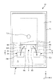
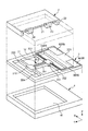
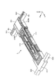
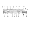
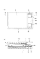
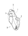
図1は、本発明の第1実施形態に係る圧力センサーモジュール(電子モジュール)の製造方法によって製造される圧力センサーモジュールを示す平面図、図2は、図1中のA−A線断面図、図3は、図1に示す圧力センサーモジュールが有する圧力センサーの分解斜視図、図4は、図3に示す圧力センサーの断面図、図5は、図3に示す圧力センサーが備える振動片の斜視図、図6は、図1に示す圧力センサーモジュールの作動を説明する断面図、図7は、本発明の第1実施形態に係る圧力センサーモジュールの製造方法を説明するための斜視図、図8は、本発明の第1実施形態に係る圧力センサーモジュールの製造方法を説明するための斜視図、図9は、本発明の第1実施形態に係る圧力センサーモジュールの製造方法を説明するための断面図、図10は、本発明の第1実施形態に係る圧力センサーモジュールの製造方法を説明するための図であって、(a)が平面図、(b)が(a)中のB−B線断面図、図11は、本発明の第1実施形態に係る圧力センサーモジュールの製造方法を説明するための図であって、(a)が平面図、(b)が(a)中のC−C線断面図、図12は、本発明の第1実施形態に係る圧力センサーモジュールの製造方法を説明するための平面図である。
なお、以下の説明では、図1中の紙面手前側を「上」、奥側を「下」と言う。他の図についてもこれに対応して説明する。また、以下では、図1に示すように、互いに直交する3軸をX軸、Y軸およびZ軸とし、Z軸を圧力センサーモジュールの厚さ方向と一致する軸とする。
Hereinafter, a method for manufacturing an electronic component and a method for manufacturing an electronic module according to the present invention will be described in detail based on embodiments shown in the accompanying drawings.
<First Embodiment>
FIG. 1 is a plan view showing a pressure sensor module manufactured by a method of manufacturing a pressure sensor module (electronic module) according to the first embodiment of the present invention, and FIG. 2 is a cross-sectional view taken along line AA in FIG. 3 is an exploded perspective view of the pressure sensor included in the pressure sensor module shown in FIG. 1, FIG. 4 is a cross-sectional view of the pressure sensor shown in FIG. 3, and FIG. 5 is a perspective view of a vibrating piece included in the pressure sensor shown in FIG. 6 is a cross-sectional view for explaining the operation of the pressure sensor module shown in FIG. 1. FIG. 7 is a perspective view for explaining a method for manufacturing the pressure sensor module according to the first embodiment of the present invention. FIG. 9 is a perspective view for explaining the manufacturing method of the pressure sensor module according to the first embodiment of the present invention, and FIG. 9 is a sectional view for explaining the manufacturing method of the pressure sensor module according to the first embodiment of the present invention. FIGS. 10A and 10B are views for explaining a method of manufacturing the pressure sensor module according to the first embodiment of the present invention, wherein FIG. 10A is a plan view, and FIG. 10B is a cross-sectional view taken along line BB in FIG. FIGS. 11A and 11B are diagrams for explaining the method of manufacturing the pressure sensor module according to the first embodiment of the present invention, where FIG. 11A is a plan view and FIG. 11B is a diagram C in FIG. -C sectional view, FIG. 12 is a plan view for explaining the method of manufacturing the pressure sensor module according to the first embodiment of the present invention.
In the following description, the front side in FIG. 1 is referred to as “up” and the back side is referred to as “down”. Other figures will be described correspondingly. In the following, as shown in FIG. 1, the three axes orthogonal to each other are defined as an X axis, a Y axis, and a Z axis, and the Z axis is defined as an axis that coincides with the thickness direction of the pressure sensor module.
1.電子モジュール
まず、本発明の電子モジュールの製造方法によって製造される電子モジュールについて説明する。なお、以下では、電子モジュールとして圧力センサーモジュール10を例に挙げて説明するが、電子モジュールとしては、圧力センサーモジュールに限定されない。
図1および図2に示すように、圧力センサーモジュール10は、圧力センサー1と、圧力センサー1を収納するパッケージ7とを有している。
1. Electronic Module First, an electronic module manufactured by the method for manufacturing an electronic module of the present invention will be described. In the following, the
As shown in FIGS. 1 and 2, the
1−1.圧力センサー
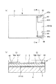
図3および図4に示すように、圧力センサー1は、ダイヤフラム層(基板)2と、振動片5が作り込まれた振動体層(振動体基板)3と、基台層4とを有しており、これら3つの層2、3、4が積層して構成されている。
ダイヤフラム層2、振動体層3および基台層4は、それぞれ、水晶で構成されているのが好ましい。このように、ダイヤフラム層2、振動体層3および基台層4を同一の材料で構成することにより、線膨張率の違いから生じる振動片5の不本意な反りや撓みを抑制することができ、圧力センサー1の検知精度を向上させることができる。特に、振動体層3を水晶で構成することにより、優れた温度特性、振動特性を有する圧力センサー1となる。
ダイヤフラム層2、振動体層3、基台層4の外形形状は、それぞれ、例えば、フォトリソグラフィ技法とドライエッチングやウエットエッチング等の各種エッチング技法とを用いて一枚の水晶平板から形成することができる。
1-1. Pressure Sensor As shown in FIGS. 3 and 4, the
The
The outer shapes of the
ダイヤフラム層2と振動体層3、および、振動体層3と基台層4は、それぞれ、低融点ガラス8を用いて接合されている。ここで、低融点ガラス8としては、特に限定されないが、水晶と線膨張率が近いバナジウム系の低融点ガラスを用いるのが好ましい。これにより、各層2、3、4と低融点ガラス8との線膨張率の違いから生じる振動片5の不本意な反りや撓みを抑制することができる。また、低融点ガラス8には、粒子状のスペーサーが含まれているのが好ましい。スペーサーを含むことにより、各層2、3、4と低融点ガラス8との線膨張率の違いから生じる振動片5の不本意な反りや撓みをより効果的に抑制することができる。なお、ダイヤフラム層2、振動体層3、基台層4の接合は、低融点ガラス8に換えて、各種接着剤を用いてもよい。
The
−ダイヤフラム層−
ダイヤフラム層2は、外部からの圧力を受けることにより変形する薄肉部21と、この薄肉部21の周囲に形成された枠部22とを有している。また、ダイヤフラム層2は、薄肉部21の下面から突出し、Y軸方向に離間して形成された一対の支持部23、24を有している。これら一対の支持部23、24には低融点ガラス8を介して振動片5が固定されている。
-Diaphragm layer-
The
−基台層−
基台層4は、振動体層3を介してダイヤフラム層2と対向して設けられている。基台層4には、上面に開放する凹部41が設けられている。この凹部41がダイヤフラム層2に形成された凹部(薄肉部21)と対向することにより空間S1が形成され、この空間S1内に振動片5が位置している。
-Base layer-
The
空間S1は、真空状態であるのが好ましい。空間S1を真空状態とすることにより、振動片5のCI(Crystal Impedance)値を低下させ、周波数安定性を向上させることができる。なお、空間S1を真空状態とするには、例えば、真空状態(真空環境下)でダイヤフラム層2、振動体層3および基台層4を接合する方法や、基台層4に貫通孔を形成しておき、常圧下でダイヤフラム層2、振動体層3および基台層4を接合した後、前記貫通孔を介して空間S1を真空状態とし、貫通孔に充填物(AuS、AuGe等)を充填し封止する方法などが挙げられる。
The space S1 is preferably in a vacuum state. By making the space S1 into a vacuum state, the CI (Crystal Impedance) value of the
−振動体層−
振動体層3は、ダイヤフラム層2と基台層4との間に配置されている。この振動体層3は、振動体31と、振動体31の周囲を囲むように設けられた枠状の枠部32と、振動体31と枠部32とを連結する4本の連結部331、332、333、334とを有している。
枠部32は、ダイヤフラム層2側から見た平面視にて、ダイヤフラム層2から露出する露出部321を有し、この露出部321に後述する導電パッド63、64がX軸方向に離間して並設されている。
-Vibration layer-
The vibrating
The
振動体31は、Y軸方向に互いに離間して設けられた一対の基部311、312と、一対の基部311、312の間に形成され、これらを連結する一対の振動ビーム313、314とを有している。振動ビーム313、314は、間隔を隔てて互いに平行にかつY軸方向に延在する長手形状をなしている。なお、振動ビームの数としては、2本に限定されず、1本であっても、3本以上であってもよい。
このような振動体31は、基部311、312にて、低融点ガラス8を介してダイヤフラム層2の支持部23、24に固定されている。
The vibrating
Such a vibrating
4本の連結部331〜334は、それぞれ、X軸方向に延在する長手形状をなし、連結部331、332が基部311と枠部32とを連結し、連結部333、334が基部312と枠部32とを連結している。なお、連結部の数や延在方向は、振動体31を枠部32に連結することができれば特に限定されず、例えば、各基部311、312に対して1本または3本以上の連結部が形成されていてもよい。
The four connecting
以上のような形状の振動体層3には、導体パターン6が形成されている。導体パターン6は、振動体31に形成された一対の励振電極61、62と、枠部32の露出部321に形成された一対の導電パッド63、64と、励振電極61、62と導電パッド63、64とを電気的に接続する配線65、66とを有している。
このうち、励振電極61、62は、振動体31とともに振動片5を構成する。励振電極61、62間に交番電圧を印加すると、振動ビーム313、314が互いに接近、離間を繰り返して振動する。
A
Among these, the
このような導体パターン6では、励振電極61、62と配線65、66とが同一工程にて形成され、導電パッド63、64は、励振電極61、62と配線65、66を形成した後に別工程によって形成されている。言い換えれば、電気的に接続されている励振電極61、配線65および導電パッド63のうち、励振電極61および配線65は、一体的に形成されており、導電パッド63は、その一部が配線65と重なるように、配線65の上から別体として形成されている。同様に、電気的に接続されている励振電極62、配線66および導電パッド64のうち、励振電極62および配線66は、一体的に形成されており、導電パッド64は、その一部が配線66と重なるように、配線66の上から別体として形成されている。
In such a
また、励振電極61、62および配線65、66は、振動体層3をダイヤフラム層2および基台層4と低融点ガラス8を介して接合する前に形成されており、導電パッド63、64は、振動体層3をダイヤフラム層2および基台層4と低融点ガラス8を介して接合した後に形成されている。このような製法とすることにより、振動体層3との密着性に優れ、かつ、電気的な接続性に優れた導電パッド63、64となる。なお、このことは、後述する圧力センサーの製造方法にて詳細に説明する。
The
1−2.パッケージ
図1および図2に示すように、パッケージ7は、ベース(搭載部)71と、ベース71に接合されたリッド(蓋体)72とによって構成されている。ベース71とリッド72との接合方法としては、特に限定されず、例えば、低融点ガラスや接着剤を用いて接合することができる。
1-2. Package As shown in FIGS. 1 and 2, the
ベース71の構成材料としては、例えば、アルミナ、シリカ、チタニア、ジルコニア等の酸化物セラミックス、窒化珪素、窒化アルミ、窒化チタン等の窒化物セラミックス等の各種セラミックスなどの絶縁性材料を用いることができる。一方、リッド72の構成材料としては、例えば、前述した各種セラミックスや、鉄、銅、アルミニウム等の各種金属材料(合金を含む)を用いることができる。
As a constituent material of the
ベース71は、箱状をなしており、その底部には一対の電極(接続電極)73、74が形成されている。一対の電極73、74は、底部の上面に形成された内部電極731、741と、底部の下面に形成された外部電極732、742と、底部を貫通し、内部電極731、741と外部電極732、742とを電気的に接続する貫通電極733、743とを有している。
リッド72は、板状をなしており、ベース71の開口を塞いでいる。これにより、パッケージ7の内部に空間Sが形成され、この空間Sに圧力センサー1が収容されている。また、リッド72には、パッケージ7の内外を連通する貫通孔721が形成されており、圧力センサーモジュール10の内外の圧力が等しく保たれている。
The
The
空間Sに収容された圧力センサー1は、接着剤によってベース71に固定されているとともに、ボンディングワイヤー(金属ワイヤー)75、76によって電極73、74と電気的に接続されている。ボンディングワイヤー75は、導電パッド63と内部電極731とを電気的に接続し、ボンディングワイヤー76は、導電パッド64と内部電極741と電気的に接続する。
The
ここで、ボンディングワイヤー75は、平面視にて、配線65と重ならないように導電パッド63に接続されている。同様に、ボンディングワイヤー76は、平面視にて、配線66と重ならないように導電パッド64に接続されている。このように、導電パッド63、64の配線65、66と重なっていない領域63b、64bにてボンディングワイヤー75、76を接続することにより、例えば、ワイヤーボンディング時にかかる応力による導電パッド63、64の剥離や破損が抑制され、これらの間の導通を確保することができるため、信頼性に優れる圧力センサーモジュール10が得られる。
Here, the
具体的には、配線65、66の表面には、圧力センサー1を構成する各層2、3、4を接合するための低融点ガラス8を溶融させる際の加熱によって金属酸化膜が形成されているおそれがある。そのため、導電パッド63、64の配線65、66と重なっている領域63a、64aでは、導電パッド63、64と配線65、66との密着強度が低い(すなわち、剥がれ易い)。これに対して、導電パッド63、64の配線65、66と重なっていない領域63b、64bでは、導電パッド63、64が振動体層3の表面に形成されているため、導電パッド63、64と振動体層3との密着強度が領域63a、64aと比較して高い(すなわち、剥がれ難い)。そのため、領域63b、64bにボンディングワイヤー75、76を接続することにより、例えば、ワイヤーボンディング時にかかる応力や使用時に受ける外力による導電パッド63、64の剥離や破損が抑制され、信頼性に優れる圧力センサーモジュール10が得られる。
Specifically, a metal oxide film is formed on the surfaces of the
以上、圧力センサーモジュール10の構成について説明した。このような圧力センサーモジュール10は、次のようにして作動する。
図6(a)に示すような圧力がダイヤフラム層2に加わると、図6(b)に示すように、2つの支持部23、24の下面が拡開するように薄肉部21が撓む。この薄肉部21の撓みによって、振動ビーム313、314に引っ張りの力が加えられる。振動片5は、振動ビーム313、314に引っ張りの応力が付与されると発振周波数が高くなる特性を有しているため、振動片5の発振周波数の変化量を検知し、検知された発振周波数の変化量に基づいて、圧力センサー1に付与された圧力の大きさを導き出すことができる。
The configuration of the
When a pressure as shown in FIG. 6A is applied to the
2.圧力センサーモジュールの製造方法
次に、上述した圧力センサーモジュール10の製造方法(本発明の電子モジュールの製造方法)について詳細に説明する。
圧力センサーモジュール10の製造方法は、圧力センサー1を製造する工程(本発明の電子部品の製造方法)と、内部電極731、741を備えているベース(パッケージベース)71を用意する工程と、ダイヤフラム層2側からの平面視にて、導電パッド63、64の配線65、66から離れている位置に内部電極731、741と接続するための金属ワイヤー75、76を配置する工程とを含んでいる。
2. Next, a manufacturing method of the
The method of manufacturing the
[圧力センサー製造工程]
圧力センサー1の製造方法は、ダイヤフラム層(構造基板)2と、励振電極61、62が配置されている振動体31および励振電極61、62と電気的に接続している配線65、66を備えている振動体層(振動体基板)3とが重なるように配置され、ダイヤフラム層2側からの平面視にて、振動体31はダイヤフラム層2に覆われ、ダイヤフラム層2側からの平面視にてダイヤフラム層2から一部が露出している振動体層3の露出部321に配線65、66の少なくとも一部を備えている接合体を用意する工程と、露出部321に一部が配線65、66と重なって電気的に接続する導電パッド63、64を形成する工程とを含んでいる。
[Pressure sensor manufacturing process]
The manufacturing method of the
−接合工程−
まず、図7に示すように、所定の外形形状を有するダイヤフラム層2、振動体層3および基台層4を用意する。なお、ダイヤフラム層2、振動体層3および基台層4は、それぞれ、例えば、フォトリソグラフィ技法とエッチング技法とを用いて水晶平板から形成することができる。
-Joining process-
First, as shown in FIG. 7, a
次に、図8に示すように、振動体層3に励振電極61、62および配線65、66を形成する。この際、配線65、66は、露出部321まで伸ばして形成する。励振電極61、62および配線65、66は、例えば、振動体層3の表面に、蒸着やスパッタリング等によってNi(ニッケル)、Cr(クロム)等からなる下地層と、Au(金)、Ag(銀)、Cu(銅)等からなる電極層とを積層してなる金属層を形成し、次に、この金属層をフォトリソグラフィ技法とエッチング技法とを用いてパターニングすることにより形成することができる。
Next, as shown in FIG. 8,
次に、図9に示すように、ダイヤフラム層2と振動体層3とを低融点ガラス8を介して接合するとともに、振動体層3と基台層4とを低融点ガラス8を介して接合する。具体的には、まず、ダイヤフラム層2、振動体層3および基台層4をこれら各層の間に低融点ガラス8を塗布して重ね合わる。次に、重ねあわせたものを両側から押圧しつつ加熱することにより低融点ガラス8を溶融させる。以上により、ダイヤフラム層2、振動体層3、基台層4が接合された接合体が得られる。
Next, as shown in FIG. 9, the
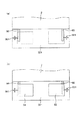
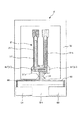
−導電パッド形成工程−
まず、図10(a)、(b)に示すように、ダイヤフラム層2上にマスクMを配置する。言い換えれば、振動体層3との間でダイヤフラム層2を挟むようにマスクMを配置する。マスクMは、平面視にて、ダイヤフラム層2の全域を覆うように設けられている。また、マスクMには、導電パッド63、64の形状(平面視形状)および形成位置に対応した開口M1、M2が形成されている。マスクMとしては、例えば、金属マスクを用いることができる。また、マスクMとしては、その他、ガラス、水晶、シリコン等の無機材料を用いることもできる。
-Conductive pad formation process-
First, as shown in FIGS. 10A and 10B, a mask M is disposed on the
次に、マスクM(開口M1、M2)を介して、蒸着やスパッタリング等によって露出部321に金属材料(蒸着材料)を付着させる(供給する)ことにより、図11(a)、(b)に示すように、導電パッド63、64を形成する。形成された導電パッド63、64は、配線65、66と重なり合う領域63a、64aと、配線65、66と重なり合わない領域63b、64bとを有している。
Next, a metal material (deposition material) is attached (supplied) to the exposed
導電パッド63、64の構成としては、特に限定されないが、例えば、Ni(ニッケル)、Cr(クロム)等からなる下地層と、Au(金)、Ag(銀)、Cu(銅)等からなる電極層とを積層した構成とすることができる。下地層を形成することにより、導電パッド63、64と振動体層3との密着性が向上する。
このように、マスクMを用いることにより、導電パッド63、64を正確に形成することができる。また、導電パッド63、64形成時におけるダイヤフラム層2への不本意な金属材料(蒸着材料)の付着を防止することができる。そのため、金属材料の付着に起因するダイヤフラム層2の不本意な反りや撓みが防止され、圧力センサー1の圧力検出精度の低下を防止することができる。
以上の工程によって、圧力センサー1が得られる。
The configuration of the
Thus, by using the mask M, the
The
[パッケージ収容工程]
まず、ベース71を用意する。ベース71は、グリーンシートを積層してなるグリーンシート積層体を焼成することにより形成することができる。また、電極73、74は、グリーンシート積層体を焼成する前にグリーンシート積層体に形成しておいてもよいし、焼成した後に形成してもよい。
[Package accommodation process]
First, the
次に、ベース71の凹部41内に接着剤を介して圧力センサー1を固定する。次に、ワイヤーボンディングによって、導電パッド63、64と内部電極731、741とを電気的に接続する。なお、ワイヤーボンディングとしては、例えば、ボールボンディング、ウェッジボンディング等の各種ボンディングを用いることができる。
この際、図12(a)に示すように、ボンディングワイヤー75の一端は、導電パッド63の配線65と重なり合っていない領域63bに接続し、ボンディングワイヤー76の一端は、導電パッド64の配線66と重なり合っていない領域64bに接続する。
Next, the
At this time, as shown in FIG. 12A, one end of the
このように、領域63b、64bにてボンディングワイヤー75、76を接続することにより、例えば、ワイヤーボンディング時にかかる応力による導電パッド63、64の剥離や破損が抑制され、これらの間の導通を確保することができる。
具体的には、配線65、66の表面には、接合工程にて加えられた熱によって金属酸化膜が形成されているおそれがある。そのため、導電パッド63、64の配線65、66と重なっている領域63a、64aでは、導電パッド63、64と配線65、66との密着強度が低い。これに対して、導電パッド63、64の配線65、66と重なっていない領域63b、64bでは、導電パッド63、64が振動体層3の表面に形成されているため、導電パッド63、64と振動体層3との密着強度が高い。そのため、領域63b、64bにボンディングワイヤー75、76を接続することにより、例えば、ワイヤーボンディング時にかかる応力による導電パッド63、64の剥離や破損が抑制され、信頼性に優れる圧力センサーモジュール10が得られる。
In this way, by connecting the
Specifically, a metal oxide film may be formed on the surfaces of the
次に、図12(b)に示すように、リッド72を用意し、ベース71の凹部開口を塞ぐようにして、リッド72をベース71に接合する。この接合は、例えば、接着剤を用いて行うことができる。
以上によって、圧力センサーモジュール10が得られる。
前述したように、圧力センサーモジュール10は、ダイヤフラム層2、振動体層3および基台層4を接合した後に、導電パッド63、64を形成するため、熱によって導電パッド63、64の表面に金属酸化膜が形成されてしまうことを効果的に抑制することができる。そのため、導電パッド63、64とボンディングワイヤー75、76との接続強度を高くすることができるとともに、これらの間の導通を確実にとることができる。さらには、ボンディングワイヤー75、76は、導電パッド63、64の配線65、66と重なっていない領域63b、64bに接続されている。このような領域は、振動体層3と強固に接合(密着)しているため、ワイヤーボンディング時などに加わる応力による導電パッド63、64の剥離、破損を効果的に防止することができる。
Next, as shown in FIG. 12B, a
Thus, the
As described above, since the
<第2実施形態>
図13は、本発明の第2実施形態に係る圧力センサーモジュールの製造方法を説明するための図であり、(a)が平面図、(b)が(a)中のD−D線断面図である。
以下、第2実施形態について、前述した実施形態との相違点を中心に説明し、同様の事項については、その説明を省略する。
第2実施形態は、圧力センサーモジュールの製造に用いられるマスクの構成が異なる以外は、第1実施形態とほぼ同様である。なお、図13では、前述した第1実施形態と同様の構成には、同一符号を付してある。
Second Embodiment
FIGS. 13A and 13B are views for explaining a method of manufacturing a pressure sensor module according to the second embodiment of the present invention, in which FIG. 13A is a plan view, and FIG. 13B is a sectional view taken along the line DD in FIG. It is.
Hereinafter, the second embodiment will be described with a focus on differences from the above-described embodiment, and description of similar matters will be omitted.
The second embodiment is substantially the same as the first embodiment except that the configuration of the mask used for manufacturing the pressure sensor module is different. In FIG. 13, the same components as those in the first embodiment described above are denoted by the same reference numerals.
図13は、前述した第1実施形態の図10に対応する図であり、「導電パッド形成工程」を示す断面図である。同図に示すように、本実施形態で用いられるマスクM’は、ダイヤフラム層2と振動体層3(露出部321)との段差を埋めるように設けられた厚肉部M3を有し、この厚肉部M3に、導電パッド63、64の形状および形成位置に対応した開口M1、M2が形成されている。
FIG. 13 is a view corresponding to FIG. 10 of the first embodiment described above, and is a cross-sectional view showing a “conductive pad forming step”. As shown in the figure, the mask M ′ used in the present embodiment has a thick portion M3 provided so as to fill the step between the
このような厚肉部M3を有することにより、マスクM’と露出部321との間の隙間(Z軸方向の長さ)を、前述した第1実施形態のマスクMを用いた場合と比較して小さくすることができる。そのため、蒸着やスパッタリングを行ったときの、開口M1、M2を通過した後の金属材料(金属材料)のまわり込みが抑制される。そのため、導電パッド63、64をより正確に形成することができる。
By having such a thick portion M3, the gap (the length in the Z-axis direction) between the mask M ′ and the exposed
特に、導電パッド63、64の輪郭を正確に形成することができるため、輪郭がぼやけて曖昧になったり、それに伴って縁部の厚さが薄くなったりするのを防止することができる。輪郭が曖昧であったり、縁部の厚さが薄かったりすると、導電パッド63、64が縁部から剥離するおそれが高まってしまう。
このような第2実施形態によっても、前述した第1実施形態と同様の効果を奏することができる。
In particular, since the contours of the
Also according to the second embodiment, the same effects as those of the first embodiment described above can be obtained.
<第3実施形態>
図14は、本発明の第3実施形態に係る圧力センサーモジュールの製造方法を説明するための平面図である。
以下、第3実施形態について、前述した実施形態との相違点を中心に説明し、同様の事項については、その説明を省略する。
第3実施形態は、各配線にアライメントマークが作り込まれている以外は、第1実施形態とほぼ同様である。なお、図14では、前述した第1実施形態と同様の構成には、同一符号を付してある。
<Third Embodiment>
FIG. 14 is a plan view for explaining the method for manufacturing the pressure sensor module according to the third embodiment of the present invention.
Hereinafter, the third embodiment will be described with a focus on differences from the above-described embodiment, and description of similar matters will be omitted.
The third embodiment is substantially the same as the first embodiment except that alignment marks are formed in each wiring. In FIG. 14, the same components as those in the first embodiment described above are denoted by the same reference numerals.
図14(a)は、圧力センサーの製造方法において、各層2、3、4の接合を終えた状態を示す図である。同図に示すように、配線65にはアライメントマーク651が形成されており、配線66には、アライメントマーク661が形成されている。
これらアライメントマーク651、661は、それぞれ、露出部321に設けられている。また、アライメントマーク651は、導電パッド63の形成領域外であってその領域の近傍に形成され、アライメントマーク661は、導電パッド64の形成領域外であってその領域の近傍に形成されている。そのため、図14(b)に示すように、導電パッド63、64を形成した状態では、アライメントマーク651、661が導電パッド63、64から露出し、重なっていない。
FIG. 14A is a diagram illustrating a state in which the bonding of the
These alignment marks 651 and 661 are provided on the exposed
このようなアライメントマーク651、661を有することにより、[パッケージ収容工程]において、導電パッド63、64にボンディングワイヤー75、76を接続する際、導電パッド63、64に対するボンディングワイヤー75、76の先端の位置決め(キャピラリーの位置決め)を簡単かつ正確に行うことができる。また、導電パッド63、64の再成膜時のアライメント精度も向上する。
By having such alignment marks 651 and 661, when connecting the
なお、本実施形態では、アライメントマーク部651、661は、配線65、66と接続されているが、これに限定されず、配線65、66と離間し、配線65、66とは別体として形成してもよい。この場合には、アライメントマーク部651、661を電気的に浮いた状態となり、配線65、66の全長を短くすることができるため、配線容量の低減を図ることができる。
また、アライメントマーク部651、661の形状としては、本実施形態のような十字に限定されず、例えば、円形、四角形等であってもよい。
このような第3実施形態によっても、前述した第1実施形態と同様の効果を奏することができる。
In this embodiment, the
In addition, the shape of the
According to the third embodiment, the same effect as that of the first embodiment described above can be obtained.
(電子機器)
次いで、圧力センサーモジュール10を備える電子機器について、図15〜図18に基づき、詳細に説明する。
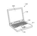
図15は、圧力センサーモジュールを備える電子機器を適用したモバイル型(またはノート型)のパーソナルコンピューターの構成を示す斜視図である。この図において、パーソナルコンピューター1100は、キーボード1102を備えた本体部1104と、表示部2000を備えた表示ユニット1106とにより構成され、表示ユニット1106は、本体部1104に対しヒンジ構造部を介して回動可能に支持されている。このようなパーソナルコンピューター1100には、外圧や操作時の指での押圧を検出するための圧力センサーモジュール10(圧力センサー1)が内蔵されている。
(Electronics)
Next, an electronic device including the
FIG. 15 is a perspective view illustrating a configuration of a mobile (or notebook) personal computer to which an electronic device including a pressure sensor module is applied. In this figure, a
図16は、圧力センサーモジュール10を備える電子機器を適用した携帯電話機(PHSも含む)の構成を示す斜視図である。この図において、携帯電話機1200は、複数の操作ボタン1202、受話口1204および送話口1206を備え、操作ボタン1202と受話口1204との間には、表示部2000が配置されている。このような携帯電話機1200には、外圧や操作時の指での押圧を検出するための圧力センサーモジュール10(圧力センサー1)が内蔵されている。
FIG. 16 is a perspective view illustrating a configuration of a mobile phone (including PHS) to which an electronic device including the
図17は、圧力センサーモジュール10を備える電子機器を適用したディジタルスチルカメラの構成を示す斜視図である。なお、この図には、外部機器との接続についても簡易的に示されている。ここで、通常のカメラは、被写体の光像により銀塩写真フィルムを感光するのに対し、ディジタルスチルカメラ1300は、被写体の光像をCCD(Charge Coupled Device)などの撮像素子により光電変換して撮像信号(画像信号)を生成する。
FIG. 17 is a perspective view illustrating a configuration of a digital still camera to which an electronic device including the
ディジタルスチルカメラ1300におけるケース(ボディー)1302の背面には、表示部が設けられ、CCDによる撮像信号に基づいて表示を行う構成になっており、表示部は、被写体を電子画像として表示するファインダーとして機能する。また、ケース1302の正面側(図中裏面側)には、光学レンズ(撮像光学系)やCCDなどを含む受光ユニット1304が設けられている。
A display unit is provided on the back of a case (body) 1302 in the
このようなディジタルスチルカメラ1300では、撮影者が表示部に表示された被写体像を確認し、シャッタボタン1306を押下すると、その時点におけるCCDの撮像信号がメモリー1308に転送・格納される。また、このディジタルスチルカメラ1300においては、ケース1302の側面に、ビデオ信号出力端子1312と、データ通信用の入出力端子1314とが設けられている。そして、図示されるように、ビデオ信号出力端子1312にはテレビモニター1430が、データ通信用の入出力端子1314にはパーソナルコンピューター1440が、それぞれ必要に応じて接続される。さらに、所定の操作により、メモリー1308に格納された撮像信号が、テレビモニター1430や、パーソナルコンピューター1440に出力される構成になっている。このようなディジタルスチルカメラ1300には、外圧や操作時の指での押圧を検出するための圧力センサーモジュール10(圧力センサー1)が内蔵されている。
In such a
図18は、圧力センサーモジュール10を備える電子機器を適用した移動体(自動車)の構成を示す斜視図である。自動車1500は、車体1501と、4つの車輪1502とを有しており、車体1501に設けられた図示しないエンジンによって車輪1502を回転させるように構成されている。このような自動車1500には、圧力センサーモジュール10(圧力センサー1)が内蔵されている。圧力センサーモジュール10は、車体1501の傾斜を検出する傾斜計や、車体1501の加速度を検出する角速度センサーモジュールとしても応用することができ、例えば、圧力センサーモジュール10からの信号に基づいて車体1501の姿勢を検出し、検出結果に応じてサスペンションの硬軟を制御したり、個々の車輪1502のブレーキを制御したりすることができる。その他、このような電子部品は、二足歩行ロボットやラジコンヘリコプターで利用することができる。
FIG. 18 is a perspective view illustrating a configuration of a moving body (automobile) to which an electronic device including the
なお、電子機器は、図15のパーソナルコンピューター(モバイル型パーソナルコンピューター)、図16の携帯電話機、図17のディジタルスチルカメラ、図18の移動体の他にも、例えば、インクジェット式吐出装置(例えばインクジェットプリンター)、ラップトップ型パーソナルコンピューター、テレビ、ビデオカメラ、ビデオテープレコーダー、カーナビゲーション装置、ページャ、電子手帳(通信機能付も含む)、電子辞書、電卓、電子ゲーム機器、ワードプロセッサー、ワークステーション、テレビ電話、防犯用テレビモニター、電子双眼鏡、POS端末、医療機器(例えば電子体温計、血圧計、血糖計、心電図計測装置、超音波診断装置、電子内視鏡)、魚群探知機、各種測定機器、計器類(例えば、車両、航空機、船舶の計器類)、フライトシュミレーター等に適用することができる。 In addition to the personal computer shown in FIG. 15 (mobile personal computer), the mobile phone shown in FIG. 16, the digital still camera shown in FIG. 17, and the movable body shown in FIG. Printer), laptop personal computer, TV, video camera, video tape recorder, car navigation device, pager, electronic notebook (including communication functions), electronic dictionary, calculator, electronic game device, word processor, workstation, videophone , Crime prevention TV monitor, electronic binoculars, POS terminal, medical equipment (for example, electronic thermometer, blood pressure monitor, blood glucose meter, electrocardiogram measuring device, ultrasonic diagnostic device, electronic endoscope), fish detector, various measuring devices, instruments (E.g. vehicle, aircraft, ship Vessels acids), it can be applied to a flight simulator or the like.
以上、本発明の電子部品の製造方法および電子モジュールの製造方法を図示の実施形態に基づいて説明したが、本発明はこれらに限定されるものではなく、各部の構成は、同様の機能を有する任意の構成のものに置換することができる。また、他の任意の構成物や、工程が付加されていてもよい。また、各実施形態を組み合せてもよい。
また、前述した実施形態において、電子部品として圧力センサーを例に挙げて説明したが、電子部品としては、これに限定されず、例えば、振動子であってもよい。また、振動子としては、音叉型の振動子、AT振動子などが挙げられる。音叉型の振動子について例を挙げて説明すると、図19に示すように、振動体層3’は、振動体31’と、露出部321を有する枠部32と、振動体31’と枠部32とを連結する連結部34とを有している。振動体31’は、基部315と、基部315から互いに並んで延出する一対の振動ビーム316、317とを有している。また、振動体層3’には、導体パターン6’が形成されている。導体パターン6’は、振動体31’に形成された一対の励振電極61’、62’と、枠部32の露出部321に形成された一対の導電パッド63、64と、励振電極61’、62’と導電パッド63、64とを電気的に接続する配線65、66とを有している。このうち、励振電極61’、62’は、振動体31’とともに振動片5’を構成する。励振電極61’、62’間に交番電圧を印加すると、振動ビーム316、317が互いに接近、離間を繰り返して振動する。
As mentioned above, although the manufacturing method of the electronic component of this invention and the manufacturing method of an electronic module were demonstrated based on embodiment of illustration, this invention is not limited to these, The structure of each part has the same function. Any configuration can be substituted. Moreover, other arbitrary structures and processes may be added. Moreover, you may combine each embodiment.
In the above-described embodiment, the pressure sensor is described as an example of the electronic component. However, the electronic component is not limited to this, and may be a vibrator, for example. Examples of the vibrator include a tuning fork vibrator and an AT vibrator. A tuning fork type vibrator will be described with reference to an example. As shown in FIG. 19, the vibrating
なお、このような振動体層3’を有する場合は、ダイヤフラムに換えてキャビティ型の蓋体を用いればよい。すなわち、層2、4で振動体31’を収納するパッケージを構成すればよい。また、電子部品を固定する搭載部としては、前述したようなパッケージのベースに換えて、回路基板等であってもよい。
また、前述した実施形態では、振動体層を水晶で構成した構成について説明したが、振動体層の構成材料としては、水晶に限定されず、例えば、タンタル酸リチウム、ニオブ酸リチウム、ホウ酸リチウム、チタン酸バリウム等の水晶以外の圧電体材料で構成することもできる。
Note that when such a vibrating
In the above-described embodiment, the configuration in which the vibrator layer is made of quartz has been described. However, the constituent material of the vibrator layer is not limited to quartz. For example, lithium tantalate, lithium niobate, lithium borate It can also be made of a piezoelectric material other than quartz such as barium titanate.
1…圧力センサー 10…圧力センサーモジュール 2…ダイヤフラム層 21…薄肉部 22…枠部 23、24…支持部 3、3’…振動体層 31、31’…振動体 311、312…基部 313、314…振動ビーム 315…基部 316、317…振動ビーム 32…枠部 321…露出部 331、332、333、334…連結部 4…基台層 41…凹部 5、5’…振動片 6、6’…導体パターン 61、61’、62、62’…励振電極 63、64…導電パッド 63a、63b、64a、64b…領域 65、66…配線 651、661…アライメントマーク 7…パッケージ 71…ベース 72…リッド 721…貫通孔 73、74…電極 731、741…内部電極 732、742…外部電極 733、743…貫通電極 75、76…ボンディングワイヤー 8…低融点ガラス 2000…表示部 1100…パーソナルコンピューター 1102…キーボード 1104…本体部 1106…表示ユニット 1200…携帯電話機 1202…操作ボタン 1204…受話口 1206…送話口 1300…ディジタルスチルカメラ 1302…ケース 1304…受光ユニット 1306…シャッタボタン 1308…メモリー 1312…ビデオ信号出力端子 1314…入出力端子 1430…テレビモニター 1440…パーソナルコンピューター 1500…自動車 1501…車体 1502…車輪 S、S1…空間 M、M’…マスク M1、M2…開口 M3…厚肉部
DESCRIPTION OF
Claims (4)
開口が形成されているマスクを前記構造基板上に配置し、前記振動体基板に、少なくとも一部が前記配線に重なっている導電パッドを形成する工程と、
を含むことを特徴とする電子部品の製造方法。 The structural substrate, the vibration body on which the excitation electrode is disposed, and the vibration body substrate including a wiring electrically connected to the excitation electrode are obtained in a plan view from the thickness direction of the vibration substrate. Preparing a joined body in which at least a part of the wiring is exposed and joined so that the vibrating body is covered with the structural substrate;
Disposing a mask having an opening formed on the structure substrate, and forming a conductive pad at least partially overlapping the wiring on the vibrator substrate;
The manufacturing method of the electronic component characterized by including.
接続電極を備えているパッケージベースと、を用意する工程と、
開口が形成されているマスクを前記構造基板上に配置し、前記振動体基板に、少なくとも一部が前記配線に重なっている導電パッドを形成する工程と、
前記接合体を前記パッケージベースに配置する工程と、
前記構造基板側からの平面視にて前記配線と重ならない位置の前記導電パッドに前記接続電極と接続するための金属ワイヤーを配置する工程と、
を含むことを特徴とする電子モジュールの製造方法。 The structural substrate, the vibration body on which the excitation electrode is disposed, and the vibration body substrate including a wiring electrically connected to the excitation electrode are obtained in a plan view from the thickness direction of the vibration substrate. A joined body in which at least a part of the wiring is exposed and the vibrator is joined so as to be covered with the structural substrate;
Providing a package base comprising connection electrodes; and
Disposing a mask having an opening formed on the structure substrate, and forming a conductive pad at least partially overlapping the wiring on the vibrator substrate;
Arranging the joined body on the package base;
Arranging a metal wire for connecting to the connection electrode on the conductive pad at a position not overlapping the wiring in a plan view from the structure substrate side;
The manufacturing method of the electronic module characterized by the above-mentioned.
前記導電パッドを形成する工程では、前記薄肉部の少なくとも一部が前記構造基板の上に配置され、且つ前記厚肉部が前記薄肉部より前記振動体基板との距離が近づくように振動体基板に対向して配置されている請求項2に記載の電子モジュールの製造方法。 The mask has a thick portion where the opening is disposed, and a thin portion having a thickness smaller than the thick portion,
In the step of forming the conductive pad, at least a part of the thin portion is disposed on the structural substrate, and the vibrating substrate is arranged such that the thick portion is closer to the vibrating substrate than the thin portion. The manufacturing method of the electronic module of Claim 2 arrange | positioned facing.
電子モジュールの製造方法。 4. The method of manufacturing an electronic module according to claim 2 , wherein an alignment mark is arranged at a position that does not overlap the conductive pad in a region of the vibrator substrate that is not covered with the structural substrate.
Priority Applications (1)
| Application Number | Priority Date | Filing Date | Title |
|---|---|---|---|
| JP2012168079A JP6089481B2 (en) | 2012-07-30 | 2012-07-30 | Method for manufacturing electronic component and method for manufacturing electronic module |
Applications Claiming Priority (1)
| Application Number | Priority Date | Filing Date | Title |
|---|---|---|---|
| JP2012168079A JP6089481B2 (en) | 2012-07-30 | 2012-07-30 | Method for manufacturing electronic component and method for manufacturing electronic module |
Publications (3)
| Publication Number | Publication Date |
|---|---|
| JP2014027585A JP2014027585A (en) | 2014-02-06 |
| JP2014027585A5 JP2014027585A5 (en) | 2015-09-10 |
| JP6089481B2 true JP6089481B2 (en) | 2017-03-08 |
Family
ID=50200819
Family Applications (1)
| Application Number | Title | Priority Date | Filing Date |
|---|---|---|---|
| JP2012168079A Expired - Fee Related JP6089481B2 (en) | 2012-07-30 | 2012-07-30 | Method for manufacturing electronic component and method for manufacturing electronic module |
Country Status (1)
| Country | Link |
|---|---|
| JP (1) | JP6089481B2 (en) |
Family Cites Families (9)
| Publication number | Priority date | Publication date | Assignee | Title |
|---|---|---|---|---|
| JPS6355537U (en) * | 1986-09-29 | 1988-04-14 | ||
| JPH0622989Y2 (en) * | 1988-05-13 | 1994-06-15 | 新光電気工業株式会社 | Package for electronic parts |
| FR2770339B1 (en) * | 1997-10-27 | 2003-06-13 | Commissariat Energie Atomique | STRUCTURE HAVING FORMED ELECTRIC CONTACTS THROUGH THE SUBSTRATE OF THIS STRUCTURE AND METHOD OF OBTAINING SUCH A STRUCTURE |
| JP3528811B2 (en) * | 2001-04-18 | 2004-05-24 | セイコーエプソン株式会社 | Method for forming electrode of piezoelectric vibrating piece, mask for forming electrode of piezoelectric vibrating piece, piezoelectric vibrator, and piezoelectric oscillator |
| DE102005015584B4 (en) * | 2005-04-05 | 2010-09-02 | Litef Gmbh | Method for producing a micromechanical component |
| JP5119756B2 (en) * | 2006-06-30 | 2013-01-16 | 株式会社デンソー | Wiring board |
| JP2009115499A (en) * | 2007-11-02 | 2009-05-28 | Alps Electric Co Ltd | Physical quantity sensor and its manufacturing method |
| JP5278147B2 (en) * | 2009-04-30 | 2013-09-04 | 大日本印刷株式会社 | Semiconductor package and semiconductor package manufacturing method |
| JP2011158342A (en) * | 2010-01-29 | 2011-08-18 | Seiko Epson Corp | Pressure sensor |
-
2012
- 2012-07-30 JP JP2012168079A patent/JP6089481B2/en not_active Expired - Fee Related
Also Published As
| Publication number | Publication date |
|---|---|
| JP2014027585A (en) | 2014-02-06 |
Similar Documents
| Publication | Publication Date | Title |
|---|---|---|
| JP6631108B2 (en) | Physical quantity sensors, sensor devices, electronic devices and moving objects | |
| JP2013232626A (en) | Electronic device, manufacturing method of the same, electronic apparatus and movable body | |
| JP5807413B2 (en) | Electronic device package, electronic device and electronic equipment | |
| JP2023166384A (en) | Vibration element, physical quantity sensor, inertial measurement unit, electronic apparatus, and movable body | |
| CN103575429B (en) | Vibrating reed, electronic installation and electronic equipment | |
| JP2015231009A (en) | Substrate for electronic device package and manufacturing method of the same | |
| JP6135370B2 (en) | Method for manufacturing functional device, electronic apparatus, and moving object | |
| JP6357759B2 (en) | Package, physical quantity sensor, electronic device and mobile | |
| JP2016176892A (en) | Angular velocity detection element, angular velocity detection device, electronic apparatus and mobile body | |
| JP6481813B2 (en) | Vibrator, vibrating device, oscillator, electronic device, and moving object | |
| JP6089481B2 (en) | Method for manufacturing electronic component and method for manufacturing electronic module | |
| JP2015231001A (en) | Electronic device and method for manufacturing electronic device | |
| JP2017015584A (en) | Electronic device, method for manufacturing electronic device, electronic apparatus, and mobile body | |
| JP5994458B2 (en) | Method for manufacturing electronic component and method for manufacturing electronic module | |
| JP2015231191A (en) | Electronic device and manufacturing method of the same | |
| JP6413316B2 (en) | Manufacturing method of vibrating piece | |
| CN105548597B (en) | Electronic device, electronic apparatus, and moving object | |
| JP6507762B2 (en) | Sensors, electronics and mobiles | |
| JP2015099061A (en) | Manufacturing method of physical quantity detection device, vibration element, physical quantity detection device and electronic apparatus | |
| JP2015050483A (en) | Electronic devices, electronic devices, and moving objects | |
| JP6492535B2 (en) | Physical quantity sensor, electronic device and mobile object | |
| JP2014153345A (en) | Sealing structure, manufacturing method of sealing structure, electronic device, electronic equipment, and mobile body | |
| JP2014197581A (en) | Lid body aggregate, method of manufacturing package, and method of manufacturing electronic device | |
| JP2014175674A (en) | Vibrator, manufacturing method of vibrator, oscillator, electronic apparatus, and movable body | |
| JP2016180739A (en) | Sensor manufacturing method, sensor, electronic device, and moving object |
Legal Events
| Date | Code | Title | Description |
|---|---|---|---|
| RD04 | Notification of resignation of power of attorney |
Free format text: JAPANESE INTERMEDIATE CODE: A7424 Effective date: 20150108 |
|
| A521 | Request for written amendment filed |
Free format text: JAPANESE INTERMEDIATE CODE: A523 Effective date: 20150723 |
|
| A621 | Written request for application examination |
Free format text: JAPANESE INTERMEDIATE CODE: A621 Effective date: 20150723 |
|
| A977 | Report on retrieval |
Free format text: JAPANESE INTERMEDIATE CODE: A971007 Effective date: 20160428 |
|
| A131 | Notification of reasons for refusal |
Free format text: JAPANESE INTERMEDIATE CODE: A131 Effective date: 20160531 |
|
| RD04 | Notification of resignation of power of attorney |
Free format text: JAPANESE INTERMEDIATE CODE: A7424 Effective date: 20160609 |
|
| RD03 | Notification of appointment of power of attorney |
Free format text: JAPANESE INTERMEDIATE CODE: A7423 Effective date: 20160613 |
|
| A521 | Request for written amendment filed |
Free format text: JAPANESE INTERMEDIATE CODE: A523 Effective date: 20160721 |
|
| TRDD | Decision of grant or rejection written | ||
| A01 | Written decision to grant a patent or to grant a registration (utility model) |
Free format text: JAPANESE INTERMEDIATE CODE: A01 Effective date: 20170110 |
|
| A61 | First payment of annual fees (during grant procedure) |
Free format text: JAPANESE INTERMEDIATE CODE: A61 Effective date: 20170123 |
|
| R150 | Certificate of patent or registration of utility model |
Ref document number: 6089481 Country of ref document: JP Free format text: JAPANESE INTERMEDIATE CODE: R150 |
|
| LAPS | Cancellation because of no payment of annual fees |