JP6087943B2 - Method for forming self-aligned contacts and local interconnects - Google Patents
Method for forming self-aligned contacts and local interconnects Download PDFInfo
- Publication number
- JP6087943B2 JP6087943B2 JP2014542328A JP2014542328A JP6087943B2 JP 6087943 B2 JP6087943 B2 JP 6087943B2 JP 2014542328 A JP2014542328 A JP 2014542328A JP 2014542328 A JP2014542328 A JP 2014542328A JP 6087943 B2 JP6087943 B2 JP 6087943B2
- Authority
- JP
- Japan
- Prior art keywords
- gate
- trench
- mandrel
- insulating layer
- insulating
- Prior art date
- Legal status (The legal status is an assumption and is not a legal conclusion. Google has not performed a legal analysis and makes no representation as to the accuracy of the status listed.)
- Active
Links
- 238000000034 method Methods 0.000 title claims description 103
- 125000006850 spacer group Chemical group 0.000 claims description 81
- 230000008569 process Effects 0.000 claims description 80
- 239000011810 insulating material Substances 0.000 claims description 62
- 239000004020 conductor Substances 0.000 claims description 50
- 239000004065 semiconductor Substances 0.000 claims description 26
- 238000004519 manufacturing process Methods 0.000 claims description 25
- 238000000151 deposition Methods 0.000 claims description 17
- 239000000758 substrate Substances 0.000 claims description 14
- 229910052751 metal Inorganic materials 0.000 claims description 13
- 239000002184 metal Substances 0.000 claims description 13
- 238000011960 computer-aided design Methods 0.000 claims description 6
- 238000003860 storage Methods 0.000 claims description 5
- 238000012545 processing Methods 0.000 claims description 4
- 238000005530 etching Methods 0.000 description 59
- 230000008021 deposition Effects 0.000 description 15
- 239000000463 material Substances 0.000 description 14
- 229910052581 Si3N4 Inorganic materials 0.000 description 13
- HQVNEWCFYHHQES-UHFFFAOYSA-N silicon nitride Chemical compound N12[Si]34N5[Si]62N3[Si]51N64 HQVNEWCFYHHQES-UHFFFAOYSA-N 0.000 description 13
- VYPSYNLAJGMNEJ-UHFFFAOYSA-N Silicium dioxide Chemical compound O=[Si]=O VYPSYNLAJGMNEJ-UHFFFAOYSA-N 0.000 description 12
- 229910052814 silicon oxide Inorganic materials 0.000 description 12
- 238000005137 deposition process Methods 0.000 description 11
- 238000002955 isolation Methods 0.000 description 8
- 230000015572 biosynthetic process Effects 0.000 description 6
- BOTDANWDWHJENH-UHFFFAOYSA-N Tetraethyl orthosilicate Chemical compound CCO[Si](OCC)(OCC)OCC BOTDANWDWHJENH-UHFFFAOYSA-N 0.000 description 5
- 230000002457 bidirectional effect Effects 0.000 description 5
- 238000005516 engineering process Methods 0.000 description 5
- WFKWXMTUELFFGS-UHFFFAOYSA-N tungsten Chemical compound [W] WFKWXMTUELFFGS-UHFFFAOYSA-N 0.000 description 5
- 229910052721 tungsten Inorganic materials 0.000 description 5
- 239000010937 tungsten Substances 0.000 description 5
- RYGMFSIKBFXOCR-UHFFFAOYSA-N Copper Chemical compound [Cu] RYGMFSIKBFXOCR-UHFFFAOYSA-N 0.000 description 4
- RTAQQCXQSZGOHL-UHFFFAOYSA-N Titanium Chemical compound [Ti] RTAQQCXQSZGOHL-UHFFFAOYSA-N 0.000 description 4
- NRTOMJZYCJJWKI-UHFFFAOYSA-N Titanium nitride Chemical compound [Ti]#N NRTOMJZYCJJWKI-UHFFFAOYSA-N 0.000 description 4
- 229910052802 copper Inorganic materials 0.000 description 4
- 239000010949 copper Substances 0.000 description 4
- 230000008878 coupling Effects 0.000 description 4
- 238000010168 coupling process Methods 0.000 description 4
- 238000005859 coupling reaction Methods 0.000 description 4
- 239000010936 titanium Substances 0.000 description 4
- 229910052719 titanium Inorganic materials 0.000 description 4
- 238000013461 design Methods 0.000 description 3
- 238000009413 insulation Methods 0.000 description 3
- 238000004544 sputter deposition Methods 0.000 description 3
- XUIMIQQOPSSXEZ-UHFFFAOYSA-N Silicon Chemical compound [Si] XUIMIQQOPSSXEZ-UHFFFAOYSA-N 0.000 description 2
- CJNBYAVZURUTKZ-UHFFFAOYSA-N hafnium(iv) oxide Chemical compound O=[Hf]=O CJNBYAVZURUTKZ-UHFFFAOYSA-N 0.000 description 2
- 238000012986 modification Methods 0.000 description 2
- 230000004048 modification Effects 0.000 description 2
- BASFCYQUMIYNBI-UHFFFAOYSA-N platinum Chemical compound [Pt] BASFCYQUMIYNBI-UHFFFAOYSA-N 0.000 description 2
- 238000005498 polishing Methods 0.000 description 2
- 229910052710 silicon Inorganic materials 0.000 description 2
- 239000010703 silicon Substances 0.000 description 2
- 239000000126 substance Substances 0.000 description 2
- 238000006467 substitution reaction Methods 0.000 description 2
- BPQQTUXANYXVAA-UHFFFAOYSA-N Orthosilicate Chemical compound [O-][Si]([O-])([O-])[O-] BPQQTUXANYXVAA-UHFFFAOYSA-N 0.000 description 1
- 229910000577 Silicon-germanium Inorganic materials 0.000 description 1
- MCMNRKCIXSYSNV-UHFFFAOYSA-N ZrO2 Inorganic materials O=[Zr]=O MCMNRKCIXSYSNV-UHFFFAOYSA-N 0.000 description 1
- LEVVHYCKPQWKOP-UHFFFAOYSA-N [Si].[Ge] Chemical compound [Si].[Ge] LEVVHYCKPQWKOP-UHFFFAOYSA-N 0.000 description 1
- 230000004888 barrier function Effects 0.000 description 1
- 230000008859 change Effects 0.000 description 1
- 239000000109 continuous material Substances 0.000 description 1
- 230000003247 decreasing effect Effects 0.000 description 1
- 230000007547 defect Effects 0.000 description 1
- 238000011161 development Methods 0.000 description 1
- 238000011982 device technology Methods 0.000 description 1
- 238000010586 diagram Methods 0.000 description 1
- 230000005669 field effect Effects 0.000 description 1
- 229910052735 hafnium Inorganic materials 0.000 description 1
- VBJZVLUMGGDVMO-UHFFFAOYSA-N hafnium atom Chemical compound [Hf] VBJZVLUMGGDVMO-UHFFFAOYSA-N 0.000 description 1
- 229910021334 nickel silicide Inorganic materials 0.000 description 1
- RUFLMLWJRZAWLJ-UHFFFAOYSA-N nickel silicide Chemical compound [Ni]=[Si]=[Ni] RUFLMLWJRZAWLJ-UHFFFAOYSA-N 0.000 description 1
- RVTZCBVAJQQJTK-UHFFFAOYSA-N oxygen(2-);zirconium(4+) Chemical compound [O-2].[O-2].[Zr+4] RVTZCBVAJQQJTK-UHFFFAOYSA-N 0.000 description 1
- 238000000059 patterning Methods 0.000 description 1
- 229910052697 platinum Inorganic materials 0.000 description 1
- 238000011165 process development Methods 0.000 description 1
- 230000009467 reduction Effects 0.000 description 1
- 235000012431 wafers Nutrition 0.000 description 1
- GFQYVLUOOAAOGM-UHFFFAOYSA-N zirconium(iv) silicate Chemical compound [Zr+4].[O-][Si]([O-])([O-])[O-] GFQYVLUOOAAOGM-UHFFFAOYSA-N 0.000 description 1
Images


Classifications
-
- H—ELECTRICITY
- H01—ELECTRIC ELEMENTS
- H01L—SEMICONDUCTOR DEVICES NOT COVERED BY CLASS H10
- H01L27/00—Devices consisting of a plurality of semiconductor or other solid-state components formed in or on a common substrate
- H01L27/02—Devices consisting of a plurality of semiconductor or other solid-state components formed in or on a common substrate including semiconductor components specially adapted for rectifying, oscillating, amplifying or switching and having potential barriers; including integrated passive circuit elements having potential barriers
- H01L27/04—Devices consisting of a plurality of semiconductor or other solid-state components formed in or on a common substrate including semiconductor components specially adapted for rectifying, oscillating, amplifying or switching and having potential barriers; including integrated passive circuit elements having potential barriers the substrate being a semiconductor body
- H01L27/08—Devices consisting of a plurality of semiconductor or other solid-state components formed in or on a common substrate including semiconductor components specially adapted for rectifying, oscillating, amplifying or switching and having potential barriers; including integrated passive circuit elements having potential barriers the substrate being a semiconductor body including only semiconductor components of a single kind
- H01L27/085—Devices consisting of a plurality of semiconductor or other solid-state components formed in or on a common substrate including semiconductor components specially adapted for rectifying, oscillating, amplifying or switching and having potential barriers; including integrated passive circuit elements having potential barriers the substrate being a semiconductor body including only semiconductor components of a single kind including field-effect components only
- H01L27/088—Devices consisting of a plurality of semiconductor or other solid-state components formed in or on a common substrate including semiconductor components specially adapted for rectifying, oscillating, amplifying or switching and having potential barriers; including integrated passive circuit elements having potential barriers the substrate being a semiconductor body including only semiconductor components of a single kind including field-effect components only the components being field-effect transistors with insulated gate
-
- H—ELECTRICITY
- H01—ELECTRIC ELEMENTS
- H01L—SEMICONDUCTOR DEVICES NOT COVERED BY CLASS H10
- H01L29/00—Semiconductor devices specially adapted for rectifying, amplifying, oscillating or switching and having potential barriers; Capacitors or resistors having potential barriers, e.g. a PN-junction depletion layer or carrier concentration layer; Details of semiconductor bodies or of electrodes thereof ; Multistep manufacturing processes therefor
- H01L29/66—Types of semiconductor device ; Multistep manufacturing processes therefor
- H01L29/68—Types of semiconductor device ; Multistep manufacturing processes therefor controllable by only the electric current supplied, or only the electric potential applied, to an electrode which does not carry the current to be rectified, amplified or switched
- H01L29/76—Unipolar devices, e.g. field effect transistors
- H01L29/772—Field effect transistors
- H01L29/78—Field effect transistors with field effect produced by an insulated gate
- H01L29/7801—DMOS transistors, i.e. MISFETs with a channel accommodating body or base region adjoining a drain drift region
- H01L29/7802—Vertical DMOS transistors, i.e. VDMOS transistors
- H01L29/7813—Vertical DMOS transistors, i.e. VDMOS transistors with trench gate electrode, e.g. UMOS transistors
-
- H—ELECTRICITY
- H01—ELECTRIC ELEMENTS
- H01L—SEMICONDUCTOR DEVICES NOT COVERED BY CLASS H10
- H01L21/00—Processes or apparatus adapted for the manufacture or treatment of semiconductor or solid state devices or of parts thereof
- H01L21/70—Manufacture or treatment of devices consisting of a plurality of solid state components formed in or on a common substrate or of parts thereof; Manufacture of integrated circuit devices or of parts thereof
- H01L21/71—Manufacture of specific parts of devices defined in group H01L21/70
- H01L21/768—Applying interconnections to be used for carrying current between separate components within a device comprising conductors and dielectrics
- H01L21/76838—Applying interconnections to be used for carrying current between separate components within a device comprising conductors and dielectrics characterised by the formation and the after-treatment of the conductors
- H01L21/76895—Local interconnects; Local pads, as exemplified by patent document EP0896365
-
- H—ELECTRICITY
- H01—ELECTRIC ELEMENTS
- H01L—SEMICONDUCTOR DEVICES NOT COVERED BY CLASS H10
- H01L21/00—Processes or apparatus adapted for the manufacture or treatment of semiconductor or solid state devices or of parts thereof
- H01L21/70—Manufacture or treatment of devices consisting of a plurality of solid state components formed in or on a common substrate or of parts thereof; Manufacture of integrated circuit devices or of parts thereof
- H01L21/71—Manufacture of specific parts of devices defined in group H01L21/70
- H01L21/768—Applying interconnections to be used for carrying current between separate components within a device comprising conductors and dielectrics
- H01L21/76801—Applying interconnections to be used for carrying current between separate components within a device comprising conductors and dielectrics characterised by the formation and the after-treatment of the dielectrics, e.g. smoothing
- H01L21/76829—Applying interconnections to be used for carrying current between separate components within a device comprising conductors and dielectrics characterised by the formation and the after-treatment of the dielectrics, e.g. smoothing characterised by the formation of thin functional dielectric layers, e.g. dielectric etch-stop, barrier, capping or liner layers
- H01L21/76832—Multiple layers
-
- H—ELECTRICITY
- H01—ELECTRIC ELEMENTS
- H01L—SEMICONDUCTOR DEVICES NOT COVERED BY CLASS H10
- H01L21/00—Processes or apparatus adapted for the manufacture or treatment of semiconductor or solid state devices or of parts thereof
- H01L21/70—Manufacture or treatment of devices consisting of a plurality of solid state components formed in or on a common substrate or of parts thereof; Manufacture of integrated circuit devices or of parts thereof
- H01L21/71—Manufacture of specific parts of devices defined in group H01L21/70
- H01L21/768—Applying interconnections to be used for carrying current between separate components within a device comprising conductors and dielectrics
- H01L21/76897—Formation of self-aligned vias or contact plugs, i.e. involving a lithographically uncritical step
-
- H—ELECTRICITY
- H01—ELECTRIC ELEMENTS
- H01L—SEMICONDUCTOR DEVICES NOT COVERED BY CLASS H10
- H01L29/00—Semiconductor devices specially adapted for rectifying, amplifying, oscillating or switching and having potential barriers; Capacitors or resistors having potential barriers, e.g. a PN-junction depletion layer or carrier concentration layer; Details of semiconductor bodies or of electrodes thereof ; Multistep manufacturing processes therefor
- H01L29/66—Types of semiconductor device ; Multistep manufacturing processes therefor
- H01L29/68—Types of semiconductor device ; Multistep manufacturing processes therefor controllable by only the electric current supplied, or only the electric potential applied, to an electrode which does not carry the current to be rectified, amplified or switched
- H01L29/76—Unipolar devices, e.g. field effect transistors
- H01L29/772—Field effect transistors
- H01L29/78—Field effect transistors with field effect produced by an insulated gate
- H01L29/7801—DMOS transistors, i.e. MISFETs with a channel accommodating body or base region adjoining a drain drift region
- H01L29/7802—Vertical DMOS transistors, i.e. VDMOS transistors
- H01L29/7809—Vertical DMOS transistors, i.e. VDMOS transistors having both source and drain contacts on the same surface, i.e. Up-Drain VDMOS transistors
-
- H—ELECTRICITY
- H01—ELECTRIC ELEMENTS
- H01L—SEMICONDUCTOR DEVICES NOT COVERED BY CLASS H10
- H01L29/00—Semiconductor devices specially adapted for rectifying, amplifying, oscillating or switching and having potential barriers; Capacitors or resistors having potential barriers, e.g. a PN-junction depletion layer or carrier concentration layer; Details of semiconductor bodies or of electrodes thereof ; Multistep manufacturing processes therefor
- H01L29/66—Types of semiconductor device ; Multistep manufacturing processes therefor
- H01L29/68—Types of semiconductor device ; Multistep manufacturing processes therefor controllable by only the electric current supplied, or only the electric potential applied, to an electrode which does not carry the current to be rectified, amplified or switched
- H01L29/76—Unipolar devices, e.g. field effect transistors
- H01L29/772—Field effect transistors
- H01L29/78—Field effect transistors with field effect produced by an insulated gate
- H01L29/7801—DMOS transistors, i.e. MISFETs with a channel accommodating body or base region adjoining a drain drift region
- H01L29/7802—Vertical DMOS transistors, i.e. VDMOS transistors
- H01L29/7812—Vertical DMOS transistors, i.e. VDMOS transistors with a substrate comprising an insulating layer, e.g. SOI-VDMOS transistors
Landscapes
- Engineering & Computer Science (AREA)
- Power Engineering (AREA)
- Microelectronics & Electronic Packaging (AREA)
- Physics & Mathematics (AREA)
- Condensed Matter Physics & Semiconductors (AREA)
- General Physics & Mathematics (AREA)
- Computer Hardware Design (AREA)
- Manufacturing & Machinery (AREA)
- Ceramic Engineering (AREA)
- Internal Circuitry In Semiconductor Integrated Circuit Devices (AREA)
- Electrodes Of Semiconductors (AREA)
- Insulated Gate Type Field-Effect Transistor (AREA)
Description
本発明は、概して、トランジスタを形成するための半導体プロセスに関し、より具体的には、半導体基板上の置換ゲート構造へのトレンチコンタクト及びローカル相互接続を形成するためのプロセスに関する。 The present invention relates generally to semiconductor processes for forming transistors, and more specifically to processes for forming trench contacts and local interconnects to replacement gate structures on a semiconductor substrate.
例えば平面トランジスタ等のトランジスタは、数十年間にわたって、集積回路のコアであり続けている。プロセス開発の進展と、フィーチャ(feature)密度の増加の必要性とを通じて、個々のトランジスタのサイズは着実に低減している。現在のスケーリングにおいては、32nm技術が用いられており、開発の進展により、20nmに進み、さらに技術を超えてきている(例えば、15nm技術)。 For example, transistors such as planar transistors have been the core of integrated circuits for decades. Through process development progress and the need for increased feature density, the size of individual transistors is steadily decreasing. In current scaling, 32 nm technology is used, and due to development progress, it has advanced to 20 nm and has further exceeded technology (for example, 15 nm technology).
置換ゲートプロセス(フロー)は、ゲートファーストプロセスにおいて見受けられる特定の問題を回避しているため、より一般的に普及してきている。例えば、置換ゲートプロセスは、ゲートにおいて用いられる仕事関数材料の安定性に関連する問題を回避することができる。しかし、置換ゲートプロセスでは、新たなプロセスモジュール(例えば、CMP(化学機械研磨))の挿入が必要となる場合がある。 Replacement gate processes (flows) have become more popular because they avoid certain problems found in gate-first processes. For example, the replacement gate process can avoid problems related to the stability of the work function material used in the gate. However, in the replacement gate process, it may be necessary to insert a new process module (for example, CMP (Chemical Mechanical Polishing)).
さらに、ほとんどの置換ゲートプロセスでは、トレンチコンタクト及び/又はローカル相互接続をゲートに形成する場合における整合問題が避けられない。例えば、ほとんどの置換ゲートプロセスは自己整合型ではないため、処理中に、不整合に起因した不具合が容易に生じ得る。また、双方向型のローカル相互接続をパターニングすること、及び/又は、ローカル相互接続からゲート若しくは当該ゲートのソース/ドレインへの界面層の数を低減することが困難になる場合がある。 Furthermore, in most replacement gate processes, alignment problems are unavoidable when forming trench contacts and / or local interconnects at the gate. For example, since most replacement gate processes are not self-aligned, defects due to mismatch can easily occur during processing. It may also be difficult to pattern bidirectional local interconnects and / or reduce the number of interface layers from the local interconnect to the gate or the source / drain of the gate.
これらの問題のうちいくつかを解消するために、自己整合型トレンチコンタクトの生成を試行するプロセスフローが提供されている。この自己整合型トレンチコンタクトは、ゲートを超えて延在することにより、より複雑度の低いローカル相互接続フローを可能にする。しかしながら、このようなプロセスフローは、極めて複雑であることが多く、多数の抵抗界面が存在し、及び、複雑なプロセスフローに起因して製造コストが高い。さらに、プロセスの複雑性に起因して、不整合又は他の誤差に対する製造マージンが低い。なぜならば、これらのプロセスは、極めて制約的な設計及び/又は整合規則を有している場合があるからである。 To overcome some of these problems, a process flow is provided that attempts to create a self-aligned trench contact. This self-aligned trench contact allows for less complex local interconnect flows by extending beyond the gate. However, such a process flow is often very complex, has a large number of resistive interfaces, and is expensive to manufacture due to the complex process flow. In addition, due to process complexity, the manufacturing margin for mismatches or other errors is low. This is because these processes may have very restrictive design and / or matching rules.
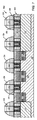
図1は、半導体基板54上の置換ゲート構造52を備えた、従来技術のトランジスタ50の実施形態を示す。置換ゲート構造52は、ゲートスペーサ58に囲まれたゲート56を含む。ソース/ドレイン60は、基板54のウェル領域62内に配置され得る。また、基板54の分離領域(isolation region)64の上方には、1つ以上のゲートが配置され得る。
FIG. 1 shows an embodiment of a
トレンチコンタクト66は、ソース/ドレイン60とローカル相互接続68Aとを接触させるのに用いられる。ローカル相互接続68Aとローカル相互接続68Bとを結合することにより、ゲート56’に接続されたローカル相互接続68Cへのルーティングが得られる。
The
図1から分かるように、トレンチコンタクト66内に任意の不整合が有る場合には、ゲート56への短絡が容易に発生し得る。そのため、制約的な設計/整合規則を用いて、トレンチコンタクト66とゲート56との間の短絡を抑制する必要がある。また、制約的な整合規則が無い場合には、ローカル相互接続68Cとゲート56’との間で整合問題が容易に発生し得る。
As can be seen from FIG. 1, if there is any mismatch in the
また、図1に示すように、ローカル相互接続68A,68B,68C間のルーティングが複雑になって、多くのプロセスステップが必要になる場合がある。このように、多数のプロセスステップがある場合には、ローカル相互接続間を形成する抵抗界面の可能性及び/又はローカル相互接続間の整合問題が増加し得る。
Also, as shown in FIG. 1, routing between the
よって、トレンチコンタクトをソース/ドレインへ自己整合させ、トレンチコンタクトをゲートの上方に延ばすための方法が必要とされている。 Therefore, there is a need for a method for self-aligning the trench contact to the source / drain and extending the trench contact above the gate.
ある実施形態では、半導体装置の製造方法は、複数の置換金属ゲートを含むトランジスタを、ソース及びドレインを有する第1のゲートと、第1のゲートから分離された少なくとも1つの第2のゲートと共に半導体基板上に設けるステップを含む。トランジスタは、各ゲートの周囲の第1の絶縁材料からなるゲートスペーサと、ゲートとゲートスペーサとの間に設けられた、第2の絶縁材料からなる第1の絶縁層とを含む。第2の絶縁材料の少なくとも一部は、第1のゲートのソース及びドレイン上に設けられる。 In one embodiment, a method of manufacturing a semiconductor device includes a transistor including a plurality of substitution metal gates, a first gate having a source and a drain, and a semiconductor with at least one second gate separated from the first gate. Providing on a substrate. The transistor includes a gate spacer made of a first insulating material around each gate, and a first insulating layer made of a second insulating material provided between the gate and the gate spacer. At least a portion of the second insulating material is provided on the source and drain of the first gate.
1つ以上の絶縁マンドレルが形成され、ゲート上に整合される。絶縁マンドレルは、第1の絶縁材料を含む。マンドレルスペーサは、絶縁マンドレルの周囲に形成される。マンドレルスペーサは、第1の絶縁材料を含む。第2の絶縁材料の第2の絶縁層は、トランジスタ上に形成される。 One or more insulating mandrels are formed and aligned on the gate. The insulating mandrel includes a first insulating material. The mandrel spacer is formed around the insulating mandrel. The mandrel spacer includes a first insulating material. A second insulating layer of the second insulating material is formed over the transistor.
絶縁マンドレル間のトランジスタの部分から第2の絶縁材料を除去することによって、第1のゲートのソース及びドレインに対する1つ以上の第1のトレンチが形成される。第2のゲートの上方の第1の絶縁材料の部分と第2の絶縁材料の部分とを除去することによって、第2のゲートに対する第2のトレンチが形成される。第1のトレンチ及び第2のトレンチに導電性材料を充填して、第1のゲートのソース及びドレインに対する第1の接点と、第2のゲートに対する第2の接点とを形成する。 By removing the second insulating material from the portion of the transistor between the insulating mandrels, one or more first trenches for the source and drain of the first gate are formed. A second trench for the second gate is formed by removing a portion of the first insulating material and a portion of the second insulating material above the second gate. The first trench and the second trench are filled with a conductive material to form a first contact to the source and drain of the first gate and a second contact to the second gate.
いくつかの実施形態では、第3の絶縁層がトランジスタ上に形成される。第3の絶縁層の部分を除去することによって、第3のトレンチが、第3の絶縁層を通じて第1のコンタクト及び第2のコンタクトへ形成される。第3の絶縁層を通じて形成された第3のトレンチに導電性材料を堆積させることによって、第1のコンタクト及び第2のコンタクトへのローカル相互接続が形成される。 In some embodiments, a third insulating layer is formed over the transistor. By removing a portion of the third insulating layer, a third trench is formed through the third insulating layer to the first contact and the second contact. A local interconnect to the first contact and the second contact is formed by depositing a conductive material in a third trench formed through the third insulating layer.
ある実施形態では、半導体装置は、半導体基板上の複数の置換金属ゲートを含む。第1のゲートは、ソース及びドレインを有しており、少なくとも1つの第2のゲートは、第1のゲートから分離されている。第1の絶縁材料のゲートスペーサは、第1のゲートの周囲に設けられている。第2の絶縁材料の第1の絶縁層は、ゲートスペーサ間に存在している。第2の絶縁材料のうち少なくとも一部は、第1のゲートのソース及びドレイン上に設けられている。 In certain embodiments, a semiconductor device includes a plurality of replacement metal gates on a semiconductor substrate. The first gate has a source and a drain, and at least one second gate is isolated from the first gate. A gate spacer of the first insulating material is provided around the first gate. A first insulating layer of a second insulating material exists between the gate spacers. At least a portion of the second insulating material is provided on the source and drain of the first gate.
1つ以上の絶縁マンドレルは、ゲート上において整合されている。絶縁マンドレルは、第1の絶縁材料を含む。マンドレルスペーサは、絶縁マンドレルの周囲に設けられており、第1の絶縁材料を含む。1つ以上の第1のゲートのソース及びドレインに対する第1のコンタクトは、マンドレルスペーサ間の第1の絶縁層を通じて設けられている。少なくとも1つの第2のゲートに対する第2のコンタクトは、第2のゲートの上方の第1の絶縁材料を通じて設けられている。第3の絶縁層はトランジスタ上に設けられており、1つ以上のローカル相互接続は、第3の絶縁層を通じて第1のコンタクト及び第2のコンタクトと接触している。 One or more insulating mandrels are aligned on the gate. The insulating mandrel includes a first insulating material. The mandrel spacer is provided around the insulating mandrel and includes a first insulating material. First contacts to the source and drain of one or more first gates are provided through a first insulating layer between the mandrel spacers. A second contact to the at least one second gate is provided through the first insulating material above the second gate. A third insulating layer is provided on the transistor, and the one or more local interconnects are in contact with the first contact and the second contact through the third insulating layer.
いくつかの実施形態では、上記の製造方法のうち1つ以上のステップが達成され、及び/又は、半導体装置の1つ以上のコンポーネントがCAD(コンピュータ支援設計)で設計されたレジストパターンによって形成される。このレジストパターンは、処理時に除去及び/又は堆積される領域を規定する。例えば、絶縁マンドレル及び/又はマンドレルスペーサを形成するための領域を、CADパターンを用いて規定することができる。ある実施形態では、コンピュータ可読記憶媒体は、複数の命令を記憶している。各命令が実行されると、1つ以上の前記レジストパターンが生成される。 In some embodiments, one or more steps of the above manufacturing method are achieved and / or one or more components of the semiconductor device are formed by a resist pattern designed by CAD (Computer Aided Design). The This resist pattern defines areas that are removed and / or deposited during processing. For example, regions for forming insulating mandrels and / or mandrel spacers can be defined using a CAD pattern. In some embodiments, the computer-readable storage medium stores a plurality of instructions. As each instruction is executed, one or more resist patterns are generated.
ゲートの上方に延びる自己整合型トレンチコンタクトを設けることによって、トレンチコンタクト及び開口ゲートへの接続に使用可能、且つ、より簡単なローカル相互接続スキームを得ることができる。本明細書に記載の方法の実施形態を用いることによって、従来の置換ゲートフロー接続スキームと比較して、トレンチコンタクトに対する下部ゲートと、ローカル相互接続結合容量とを得ることができ、且つ、層間の抵抗界面の数を低減することができる。また、本明細書に記載の方法の実施形態によって、コンタクト間の不整合の可能性を低減し、且つ、従来の置換ゲートフロー接続スキームよりも簡単なプロセスフローを提供することができ、製造歩留まりを向上させることができる。 By providing a self-aligned trench contact extending above the gate, a simpler local interconnection scheme can be obtained that can be used to connect to the trench contact and the open gate. By using an embodiment of the method described herein, a lower gate for the trench contact and local interconnect coupling capacitance can be obtained compared to conventional replacement gate flow connection schemes, and between the layers. The number of resistance interfaces can be reduced. Also, the method embodiments described herein can reduce the possibility of misalignment between contacts and provide a simpler process flow than conventional replacement gate flow connection schemes, resulting in manufacturing yield. Can be improved.
本明細書では、本発明におけるいくつかの実施形態及び例示的な図面について例示的に述べるが、当業者であれば、本発明は記載の実施形態又は図面に限定されないことを認識するであろう。図面及び本明細書における詳細な説明は、本発明を開示の特定の形態に限定するものではなく、本発明が、添付の特許請求の範囲によって規定されるような本発明の意図及び範囲に含まれる全ての改変、均等及び代替を網羅することが理解されるであろう。本明細書において用いられる全ての項目は、ひとえに分類目的のためのものであり、本記載又は特許請求の範囲を限定することを意図するものではない。本明細書において用いられる「〜し得る(may)」という単語は、必須である(すなわち、必ず必要である)という意味としてではなく、許容的な意味合いとして用いられる(すなわち、可能性の意味合いとして用いられる)。同様に、「含む(include)」という用語は、非限定的に含むという意味を含む。 Although several embodiments and exemplary drawings of the invention are described herein by way of example, those skilled in the art will recognize that the invention is not limited to the described embodiments or drawings. . The drawings and detailed description are not intended to limit the invention to the particular forms disclosed, but are intended to be within the spirit and scope of the invention as defined by the appended claims. It will be understood to cover all modifications, equivalents and alternatives that may be made. All items used herein are for classification purposes only and are not intended to limit the scope of this description or the claims. As used herein, the word “may” is used as an acceptable meaning (ie, as a possible meaning), not as an essential (ie, necessarily required) meaning. Used). Similarly, the term “include” includes meaning including but not limited to.
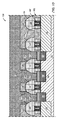
図2は、一実施形態における、トランジスタ100を形成するシリコン基板上の置換金属ゲート構造の縦断側面図である。トランジスタ100は、当該技術分野において周知の任意の種類のトランジスタであってよい。例えば、トランジスタ100は、平面トランジスタ(例えば、平面電界効果トランジスタ(FET))又は非平面トランジスタ(例えば、FinFETトランジスタ)であってよい。
FIG. 2 is a longitudinal side view of a replacement metal gate structure on a silicon
ある実施形態では、トランジスタ100は、基板101上に形成された置換金属ゲート構造102を含む。ゲート構造102は、当該技術分野において周知のプロセス(例えば、置換ゲートプロセスであるが、これに限定されない)によって、基板101上に形成されている。図2に示すように、ゲート構造102は、ゲートスペーサ106によって囲まれたゲート104を含む。ゲート104は、基板101のウェル領域108(トランジスタ100の活性領域)の上方に形成され、及び/又は、トレンチ分離110(トランジスタの分離領域)の上方に形成されてもよい。トレンチ分離110は、いくつかの実施形態において、浅いトレンチ分離であってよい。
In some embodiments,
ある実施形態では、ソース/ドレイン112は、基板101のウェル領域108内に形成されている。いくつかの実施形態では、ソース/ドレインは、プラチナバリア層112Bによって分離された、埋設されたシリコンゲルマニウム(eSiGe)層112A及びニッケルシリサイドコンタクト112Cを含む。当該技術分野において周知の他の種類のソース/ドレインも利用可能である。
In some embodiments, source /
ある実施形態では、ゲート104は、金属ゲート104A(例えば、置換金属ゲート)であり、高K(高誘電率)材料104B上に形成されている。図2中、各符号(104A,104B)を、明確さのために左端ゲートのみに示す。上述したように、金属ゲート104A及び高K材料104Bは、置換ゲートプロセスを用いて形成されてもよい。金属ゲート104Aは、金属(例えば、チタン、タングステン、窒化チタン又はこれらの組み合わせであるが、これらに限定されない)を含んでもよい。高K材料104Bは、誘電体(例えば、ケイ酸ハフニウム、ケイ酸ジルコニウム、二酸化ハフニウム、二酸化ジルコニウム又はこれらの組み合わせであるが、これらに限定されない)を含んでもよい。
In some embodiments, the
図2に示すように、ゲート104及びゲートスペーサ106は、絶縁層114によって囲まれている。ある実施形態では、ゲートスペーサ106及び絶縁層114は、異なる絶縁材料から形成されているので、ゲートスペーサと絶縁層との間にエッチング選択性を得ることができる。例えば、ゲートスペーサ106は、窒化ケイ素から形成されてもよく、絶縁層114は、TEOS(オルトケイ酸テトラエチル)堆積から形成された酸化ケイ素であってよい。
As shown in FIG. 2, the
ある実施形態では、図2に示す置換金属ゲート構造102は、例えば化学機械研磨(CMP)によって平坦化されている。ゲート構造102の平坦化後に、図3に示すように、絶縁層116がゲート構造上に形成(堆積)される。ある実施形態では、絶縁層116は、窒化ケイ素、又は、ゲートスペーサ106と同じ絶縁材料を含む。絶縁層116は、当該技術分野において周知の方法(例えば、プラズマ蒸着であるが、これに限定されない)を用いて形成されてもよい。ある実施形態では、絶縁層116は、平面の(非コンフォーミング(non−conforming)な)堆積プロセスを用いて形成される。ゲート構造が絶縁層に封入されるように、絶縁層116がゲート構造102上に形成される。
In some embodiments, the replacement
いくつかの実施形態では、図4に示すように、薄い絶縁層118は、ゲート構造と絶縁層116との間のゲート構造102上に形成(堆積)される。薄い絶縁層118は、酸化ケイ素、又は、絶縁層114と同じ絶縁材料を含んでもよい。
In some embodiments, a thin
絶縁層116の堆積後に、絶縁層116のうち選択された部分を除去して、図5に示すように、絶縁マンドレル120をゲート104上に形成することができる。簡潔さのため、以降の図において全てのコンポーネント(例えば、各ゲート104又はゲートスペーサ106)に参照符号を付すわけではない。各マンドレル120は、下側のゲート104とほぼ同じ幅を有するように形成されてもよい。ある実施形態では、各マンドレル120は、少なくとも下側のゲート104と同じ幅である(例えば、マンドレルの最小幅は、少なくとも下側のゲートの幅と同じであるが、マンドレルは、下側のゲートよりも若干幅広に形成されてもよい)。よって、各マンドレル120の縁部は、少なくとも下側のゲート104の縁部を超えて延びる。いくつかの場合において、整合問題及び/又は他の製造問題に起因して、1つ以上のマンドレル120の幅は、下側のゲートの幅よりも小さい。マンドレルの幅は、当該技術分野において周知のインライン計測技術を用いて評価することができる。マンドレルが下側のゲートほど幅広いではない場合には、そのより狭い幅は、本明細書にて記載される後続の処理ステップ時において、マンドレルスペーサ幅を用いるために補償され得る。
After deposition of the insulating
マンドレル120は、絶縁層116を、レジストパターン又はマスクによってパターニングすることによって、形成され得る。このレジストパターン又はマスクは、絶縁層のうち選択された部分を除去するように設計されており、その結果、残りの部分によって、ゲート104の上方のマンドレルが形成される。マンドレル120の形成に用いられるレジストパターン又はマスクは、CAD(コンピュータ支援設計)で設計されたパターン又はマスク(例えば、CAD設計されたレジストパターン)であってよい。ある実施形態では、コンピュータ可読記憶媒体は、複数の命令を記憶している。各命令が実行されると、レジストパターン又はマスク設計(例えば、マンドレル120の形成に用いられる、CAD設計されたレジストパターン又はマスクであるが、これに限定されない)が生成される。いくつかの実施形態において、マンドレル120の形成に用いられるレジストパターン及び/又はマスクは、ゲート104の形成に用いられるレジストパターン及び/又はマスクと同じである。同じレジストパターン及び/又はマスクを用いることにより、マンドレル120は、ゲート104とほぼ同じ限界寸法(例えば、幅)を有することが可能になる。
The
絶縁層116のうち、レジストパターン又はマスクによる除去対象として選択された部分は、例えば、絶縁層のうち選択された部分のエッチングによって除去することができる。いくつかの実施形態において、絶縁層116のエッチングは、時限エッチングである。エッチングプロセスを時限的に行うことにより、エッチングは絶縁層114において停止する。いくつかの実施形態において、絶縁層116のエッチングに用いられるエッチングプロセスは、絶縁層116と絶縁層114との間において選択的に行われるため、絶縁層116の絶縁材料がエッチングされるのに対し、絶縁層114の絶縁材料はエッチングされない。例えば、エッチングプロセスにおいて、絶縁層116に用いられている窒化ケイ素はエッチングされるのに対し、絶縁層114に用いられている酸化ケイ素はエッチングされない。エッチングプロセスを時限的に行って絶縁層114で停止させることにより、ゲートスペーサ106へのエッチングの原因となり得るオーバーエッチングが無くなる。いくつかの実施形態において、エッチング停止層(例えば、図4に示す薄い絶縁層118)は、絶縁層116のエッチング時におけるオーバーエッチングを抑制するためのベース層として用いられる。
A portion of the insulating
マンドレル120の形成後に、図6に示すように、絶縁層122を、マンドレル及び絶縁層114上に形成(堆積)させる。ある実施形態では、絶縁層122は、窒化ケイ素、又は、マンドレル120と同じ絶縁材料を含む。絶縁層122は、当該技術分野において周知の方法(例えば、プラズマ蒸着であるが、これに限定されない)を用いて形成されてもよい。ある実施形態では、絶縁層122は、非平面又はコンフォーマル(conformal)な堆積プロセスを用いて形成される。非平面の堆積プロセスを用いることにより、図6に示すように、材料が堆積される表面(例えば、マンドレル120)に絶縁材料が適合する。
After the
絶縁層122の堆積後に、絶縁層の部分を除去(エッチバック)して、図7に示すように、マンドレルスペーサ124を形成する。マンドレルスペーサ124は、マンドレル120の周囲に形成されてもよく、マンドレルの側部(縁部)に隣接する。マンドレルスペーサ124は、絶縁層122の一部をエッチングプロセスによって除去することにより、形成され得る。このエッチングプロセスでは、側方と比べて下方に高速にエッチングされる。よって、エッチングプロセスにより、絶縁層材料は、垂直表面(例えば、側壁)よりも水平表面において高速に、好ましく除去される。エッチングパラメータ(例えば、エッチングプロセス時におけるエッチングバイアス及びエッチング時間)を制御することにより、マンドレルスペーサ124の最終幅を制御することができる。
After the insulating
いくつかの実施形態において、マンドレルスペーサ124の高さは、マンドレル120の高さと同様である。図6に示す絶縁層122の非平面(コンフォーマル)堆積に起因して、マンドレルスペーサ124は、図7に示すようにスペーサの上部から下部にかけてテーパー状(傾斜状)の外形を有する。そのため、マンドレルスペーサ124は、下部においてより幅広になっており、上部においてより幅狭になっている。
In some embodiments, the height of the
ある実施形態では、マンドレルスペーサ124の幅は、マンドレルスペーサ124の縁部がゲートスペーサ106の縁部を超えて延びるような幅になっている。絶縁層122の一部を除去する際に用いられるエッチングプロセスを調節すること(例えば、エッチングプロセス時におけるエッチングレート及び/若しくは選択性を制御すること)並びに/又はマンドレルスペーサの形成に用いられる絶縁層の堆積時における絶縁層122の厚さを調節することにより、マンドレルスペーサ124の幅を調節することができる。エッチングプロセス及び/又は堆積厚さの調節によってマンドレルスペーサ124を調節することが可能となることにより、マンドレルスペーサの幅を、ロット単位又はウェーハ単位で制御することが可能になる。
In some embodiments, the width of the
マンドレルスペーサ124の形成後に、図8に示すように、絶縁層126を、マンドレル120、マンドレルスペーサ及び絶縁層114上に形成(堆積)させる。ある実施形態では、絶縁層126は、酸化ケイ素、又は、絶縁層114と同じ絶縁材料を含む。絶縁層126は、当該技術分野において周知の方法(例えば、TEOS堆積であるが、これに限定されない)を用いて形成することができる。ある実施形態では、絶縁層126は、平面堆積プロセスを用いて形成される。マンドレル120及びマンドレルスペーサ124が絶縁層に封入されるように、絶縁層126を形成することができる。
After the formation of the
絶縁層126の形成後に、図9に示すように、絶縁層126及び絶縁層114を通じてソース/ドレイン112へトレンチ128を形成することができる。絶縁層126及び絶縁層114が同じ絶縁材料から形成されているため、単一のエッチングプロセスを用いてトレンチ128を形成することができる。絶縁層126及び絶縁層114の絶縁材料(例えば、酸化ケイ素)のエッチングに対しては選択的であって、且つ、マンドレル120及びマンドレルスペーサ124の絶縁材料(例えば、窒化ケイ素)のエッチングに対しては選択的ではないエッチングプロセスを用いて、トレンチ128を形成することができる。
After the formation of the insulating
マンドレルスペーサ124の少なくとも一部は、トレンチ128において露出される。トレンチ128の外形は、マンドレルスペーサ124の存在と、マンドレルスペーサの傾斜状の外形とに起因して、上部においてより幅広となっており、且つ、下部においてより幅狭の傾斜状になっている。そのため、トレンチ128の傾斜は、マンドレルスペーサ124の傾斜によって決定される。トレンチ128を形成する際に選択的エッチングを用いることにより、ゲート104の縁部及びゲートスペーサ106上に形成された、マンドレルスペーサ124の一部が除去されるのを抑制することができる。トレンチ128におけるマンドレルスペーサ124の幅及び外形を維持することにより、トレンチ、マンドレル120、マンドレルスペーサ又はゲートにおいて何らかの不整合が有る場合でも、ゲート104の露出部分が、トレンチを充填するための材料と接触するのを抑制することができる。
At least a portion of the
トレンチ128の形成後に、トレンチを、図10に示すように導電性材料130で充填する。導電性材料130は、例えば、タングステン、銅、チタン、窒化チタン又はこれらの組み合わせであってもよいが、これらに限定されない。導電性材料130は、当該技術分野において周知の方法(例えば、スパッタリング又は無電解析出であるが、これらに限定されない)を用いて、導電性材料の層として形成されてもよい。ある実施形態では、導電性材料130は、下方の層を導電性材料内に封入する平面堆積プロセスを用いて形成される。下方の層を導電性材料130内に封入することにより、導電性材料を、トレンチ128に完全に充填することができる。
After formation of
トレンチ128に導電性材料130を充填した後に、トランジスタ100を、図11に示すように平坦化することができる。トランジスタ100の平坦化は、例えば、トランジスタのCMPによって行うことができる。トランジスタ100の平坦化は、マンドレル120の上部及びマンドレルスペーサ124が平面表面において露出されるように材料を除去することを含み得る。トランジスタ100の平坦化の後に、トレンチ128内の導電性材料130により、ソース/ドレイン112に対するトレンチコンタクト132が形成される。
After filling the
トレンチコンタクト132は、トレンチ128の外形と共に形成され、下部よりも上部において幅広となる。そのため、トレンチコンタクト132の傾斜は、マンドレルスペーサ124の傾斜によって決定される。マンドレルスペーサ124及びトレンチコンタクト132の外形を傾斜させることにより、トレンチコンタクト132の導電性材料130が、ゲート104と接触(短絡)するのを抑制することができる。例えば、従来技術の装置の場合には、ゲート、トレンチコンタクトの形成時、又は、他のプロセスステップの実行時において少しでも不整合が有ると、トレンチコンタクトとゲートとの間の短絡が発生し得る。図11に示すように、マンドレルスペーサ124は、ゲート104の縁部(及びゲートスペーサ106)を超えて延びた下部が、より幅広の外形となっているため、トレンチ接点132とゲート104との間において短絡が発生する可能性がほとんど無く、トレンチコンタクトは自己整合する。
The
ある実施形態では、マンドレルスペーサ124の傾斜及び幅に起因して、トレンチコンタクトの下部の限界寸法が低減するため、ゲート104からトレンチコンタクト132への容量結合が低下する。いくつかの実施形態において、ゲート104は幅広となる。ゲート104の幅広化は、トレンチコンタクト132に対する短絡の可能性の増加を招くこと無く、行うことが可能である。なぜならば、マンドレルスペーサ124の傾斜及び幅に起因して、ソース/ドレイン112上のトレンチコンタクトが自己整合するからである。ゲート104を幅広化することにより、漏洩の低減、電力低減の促進及び動作特性の増加となる。トレンチコンタクト132の自己整合により、製造マージンも増加する(例えば、短絡又は不整合などの製造問題の可能性が低下する)。
In some embodiments, due to the tilt and width of the
平坦化プロセスの後に、図12に示すように、トランジスタ100の平面表面上に絶縁層134を形成(堆積)させる。ある実施形態では、絶縁層134は、窒化ケイ素、又は、マンドレル120及びマンドレルスペーサ124と同じ絶縁材料を含む。絶縁層134は、当該技術分野において周知の方法(例えば、プラズマ蒸着であるが、これに限定されない)を用いて形成することができる。ある実施形態では、絶縁層134は、平面堆積プロセスを用いて形成される。絶縁層134は、下方の層を封入する薄い絶縁層であってよい。
After the planarization process, an insulating
ある実施形態では、図13に示すように、絶縁層136を絶縁層134上に形成(堆積)する。ある実施形態では、絶縁層136は、酸化ケイ素、又は、絶縁層114,116と同じ絶縁材料を含む。絶縁層136は、当該技術分野において周知の方法(例えば、TEOS堆積であるが、これに限定されない)を用いて形成され得る。ある実施形態では、絶縁層136は、平面堆積プロセスを用いて形成される。絶縁層136は、下方の絶縁層134を封入する厚い絶縁層であってよい。
In some embodiments, an insulating
絶縁層136の堆積の後に、図14に示すように、絶縁層136及び絶縁層134を通じてトレンチコンタクト132までのトレンチ138を形成する。ある実施形態では、トレンチ138は、トレンチコンタクト132及びソース/ドレイン112へのローカル相互接続のために用いられる。図14に示すように、トレンチコンタクト132は、上部が幅広の外形となっているため、トレンチ138(及びトレンチを用いて得られるローカル相互接続)とトレンチコンタクトとの間の整合の許容性を向上させる。
After the insulating
ある実施形態では、トレンチ138は、2ステップエッチングプロセスを用いて形成される。第1のステップにおいて、絶縁層134をエッチング停止層として用いて、絶縁層136がエッチング(酸化ケイ素エッチング)され得る。第2のステップにおいて、絶縁層134(窒化ケイ素)を通じてトレンチコンタクト132まで、エッチングが行われ得る。
In some embodiments,
ある実施形態では、図15に示すように、トレンチ140が、絶縁層136を通じて形成される。トレンチ140は、絶縁層134をエッチング停止層として用いて、絶縁層136から絶縁層134を通じて形成され得る。トレンチ140を用いて、ゲート104’(図15において右側のゲート)へのローカル相互接続経路を形成することができる。ゲート104’は、トランジスタ100内の他のゲートから分離され得る(例えば、ゲート104’は、トランジスタの分離領域内に存在し、その他のゲートは、活性領域内に存在する)。トレンチ140及びトレンチ138を、ゲート104’以外のゲートの上方において組み合わせることにより、ゲート104’への接続を行うことなく、ローカル相互接続を結合することが可能になる。
In some embodiments, a
トレンチ140を形成した後に、ゲート開口トレンチ142をゲートの上方に形成して、図16に示すように、ゲート104’へ接続することができる。トレンチ142は、ゲート開口トレンチであってよい。ゲート104’の上方のマンドレル120及びマンドレルスペーサ124を通じて、例えば窒化ケイ素エッチングプロセスを用いたエッチングを行うことにより、トレンチ142を形成することができる。トレンチ142を用いてゲート104’への接続を得ることによって、トランジスタ100内の他のゲートへの接続を用いること無く、ゲートを選択的に接続することが可能になる。エッチングプロセスは、時限エッチングプロセスであってよく、ゲート104’の周囲のゲートスペーサ106への有意なオーバーエッチングを制限する。ある実施形態では、トレンチ142を形成するためのエッチングプロセスは、自己整合プロセスである。なぜならば、エッチングプロセスは、マンドレル120及びマンドレルスペーサ124の絶縁材料(例えば、窒化ケイ素)に対して選択的であって、絶縁層114(酸化ケイ素)までエッチングしないからである。トレンチ138、トレンチ140及びトレンチ142の組み合わせを用いることにより、(ソース/ドレイン112と接触する)トレンチコンタクト132とゲート104’との間のルーティングのための簡単且つ双方向型のローカル相互接続スキームが得られる。
After forming the
いくつかの実施形態において、絶縁層136の絶縁材料のための第1のエッチングプロセスを用いて、トレンチ140と、絶縁層136内のトレンチ138の部分とを形成することができる。その後、第2のエッチングプロセスを用いて、トレンチ140の下方の絶縁層134がエッチングされることを回避するためのマスクを用いて、トレンチ138内の絶縁層134の部分を除去することができる。いくつかの実施形態において、絶縁層134のための第2のエッチングプロセスを用いて、ゲート104’へのトレンチ142を形成することもできる。
In some embodiments, the first etching process for the insulating material of the insulating
トレンチ138、トレンチ140及びトレンチ142に導電性材料を充填することにより、図17に示すように、ローカル相互接続144A,144B,144Cが形成される。ある実施形態では、トレンチ138,トレンチ140,トレンチ142に対して導電性材料を同時に充填する。ローカル相互接続144A,144B,144Cの形成に用いられる導電性材料は、トレンチコンタクト132の形成に用いられる材料(例えば、タングステン又は銅)と同じ材料であってよい。ある実施形態では、ローカル相互接続144A,144B,144Cは、双方向型のルーティング及びゲート開口トレンチ142の利用に起因して、他のルーティングスキームにおいて用いられるローカル相互接続よりも肉厚である。より肉厚のローカル相互接続を用いることにより、ローカル相互接続層における抵抗が低下するため、トランジスタ性能が向上する。
Filling
ある実施形態では、トレンチ138、トレンチ140及びトレンチ142に導電性材料を充填した後に、トランジスタ100を(例えば、CMPを用いて)平坦化させて、図17に示す平面表面を形成する。図18に示すトランジスタ100の別の実施形態が図17に示す実施形態と異なる点は、図4に示した薄い絶縁層118が絶縁層116の下方に用いられている点にある。
In some embodiments, after filling
図15〜図18に示すように、ローカル相互接続144Cを形成するプロセスは、比較的大きな段差高さでエッチング(トレンチ形成)及び/又はトレンチ充填を行うことを含む。例えば、図16に示すように、ゲート開口トレンチ142を、絶縁層136のトレンチ140を通じてゲート104’まで形成した場合には、大きなステップ高さが発生する。このような大きなステップ高さの場合には、プロセス時における高さ変化が大きいため、制御可能な態様でエッチング及び充填を行うことが困難になる場合がある。例えば、装置の上面(絶縁層136の上部)とゲート104’の上面との間の高さに大きな差があるため、ゲート開口トレンチ142のアスペクト比の制御が困難になる場合がある。
As shown in FIGS. 15-18, the process of forming the local interconnect 144C includes performing etching (trench formation) and / or trench filling at a relatively large step height. For example, as shown in FIG. 16, when the
大きな段差高さに起因する問題に対処し、より歩留まりの良いより簡単なプロセスフローを提供するために、ゲート開口トレンチ及びトレンチコンタクトの充填を単一のプロセスで行うことが可能なプロセスを提供することが可能である。ゲート開口トレンチ及びトレンチコンタクトを同時に充填することにより、より簡単なプロセスが可能になり、ゲート開口へのローカル相互接続に関連するエッチングステップ及び充填ステップ時における段差を低減することができる。 Provide a process that can fill gate opening trenches and trench contacts in a single process to address the problems caused by large step heights and provide a simpler process flow with better yield It is possible. By simultaneously filling the gate opening trench and trench contact, a simpler process is possible and steps during the etching and filling steps associated with local interconnection to the gate opening can be reduced.
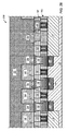
図19〜図29は、図8に示すトランジスタ100の構造から連続するトレンチコンタクト及びローカル相互接続を形成するための別のプロセスを用いて形成されたトランジスタ200の構造の縦断側面図である(例えば、トランジスタ200は、トランジスタ100の別の実施形態である)。図8に示すように絶縁層126を形成した後に、図19に示すように、レジスト202から形成されたレジストパターンを用いて、トレンチ128を、絶縁層126及び絶縁層114を通じてソース/ドレイン112へ形成する。絶縁層126及び絶縁層114の絶縁材料(例えば、酸化ケイ素)を選択的にエッチングし、且つ、マンドレル120及びマンドレルスペーサ124の絶縁材料(例えば、窒化ケイ素)をエッチングしないエッチングプロセスを用いて、トレンチ128を形成することができる。
19-29 are longitudinal side views of a structure of
トレンチ128の形成後に、レジスト202から形成された別のレジストパターンを用いてトランジスタ200をパターニングして、図20に示すように、ゲート開口トレンチ142を形成する。第1のエッチングプロセス(例えば、酸化ケイ素エッチングプロセス)を用いて絶縁層126をマンドレル120までエッチングした後に、ゲート104’(分離ゲート)の上方のマンドレル120及びマンドレルスペーサ124を通じて第2のエッチングプロセス(例えば、窒化ケイ素エッチングプロセス)を用いたエッチングを行うことにより、トレンチ142を形成することができる。いくつかの実施形態において、マンドレル120及びマンドレル124は、第1のエッチングプロセスのためのエッチング停止層として用いられる。いくつかの実施形態において、第3のエッチングプロセスは、絶縁層118(図4に示す)を通じたエッチングのために必要であってよい。絶縁層118は、第2のエッチングプロセスのためのエッチング停止層として用いられ得る。
After the
いくつかの実施形態において、上記のエッチングプロセスのうち1つ以上は時限エッチングプロセスであり、有意なオーバーエッチング(例えば、ゲート104’の周囲のゲートスペーサ106へのエッチング)を制限する。ある実施形態では、トレンチ142を形成するための第2のエッチングプロセスは、自己整合プロセスである。なぜならば、第2のエッチングプロセスは、マンドレル120及びマンドレルスペーサ124の絶縁材料(例えば、窒化ケイ素)に対して選択的であって、絶縁層114(酸化ケイ素)までエッチングしないからである。
In some embodiments, one or more of the etching processes described above is a timed etching process that limits significant over-etching (eg, etching into the
図20に示すように、ゲート開口トレンチ142は、トレンチ128の形成直後に形成されるため、ゲート開口トレンチを形成するためのエッチングプロセスは、(トレンチ128とゲート開口トレンチ142とを形成する間に中間ステップがいくつか必要となる)図16について述べたゲート開口トレンチの形成のためのエッチングよりも浅い。より浅いエッチングプロセスにより、ゲート開口トレンチ142のアスペクト比の制御が向上する。図20に示すように、ゲート開口トレンチ142のためのレジストパターンの形成のために用いられるレジスト202によってトレンチ128を充填して、ゲート開口トレンチの形成時におけるトレンチ128のエッチングを抑制する。
As shown in FIG. 20, since the
ゲート開口トレンチ142の形成後にレジスト202を除去して、図21に示すように、トレンチ128及びゲート開口トレンチを露出させる。トレンチ128及びゲート開口トレンチ142は、相対的に類似する段差高さを有する。レジスト除去後に、図22に示すように、導電性材料130をトレンチ128及びゲート開口トレンチ142に充填する。ある実施形態では、単一のプロセス(例えば、同一プロセス)で導電性材料130をトレンチ128及びゲート開口トレンチ142に充填する。
After the
導電性材料130は、例えば、タングステン、銅、チタン、窒化チタン又はこれらの組み合わせを含み得るが、これらに限定されない。当該技術分野において周知の方法(例えば、スパッタリング又は無電解析出であるが、これらに限定されない)を用いて、導電性材料130を導電性材料の層として形成することができる。ある実施形態では、下方の層を導電性材料に封入する平面堆積プロセスを用いて、導電性材料130を形成する。下方の層を導電性材料130に封入することにより、導電性材料をトレンチ128及びゲート開口トレンチ142に完全に充填することができる。
The
導電性材料130をトレンチ128及びゲート開口トレンチ142に充填した後に、図23に示すように、トランジスタ200が平坦化され得る。トランジスタ200の平坦化は、例えばトランジスタのCMPによって行われ得る。トランジスタ200を平坦化することは、マンドレル120及びマンドレルスペーサ124の上部が平面表面において露出するように材料除去を行うことを含み得る。トランジスタ200の平坦化後に、トレンチ128内の導電性材料130によって、ソース/ドレイン112へのトレンチコンタクト132が形成され、ゲート開口トレンチ142内の導電性材料130によって、ゲート104’へのゲート開口トレンチコンタクト204が形成される。
After filling the
平坦化プロセスの後に、図24に示すように、絶縁層134及び絶縁層136がトランジスタ200の平面表面上に形成(堆積)される。ある実施形態では、絶縁層134は、窒化ケイ素、又は、マンドレル120及びマンドレルスペーサ124と同じ絶縁材料を含む。絶縁層134は、当該技術分野において周知の方法(例えば、プラズマ蒸着であるが、これに限定されない)を用いて形成することができる。ある実施形態では、絶縁層134は、平面堆積プロセスを用いて形成される。絶縁層134は、下方の層を封入する薄い絶縁層であってよい。
After the planarization process, an insulating
ある実施形態では、絶縁層136は、酸化ケイ素、又は、絶縁層114,116と同じ絶縁材料を含む。絶縁層136は、当該技術分野において周知の方法(例えば、TEOS堆積であるが、これに限定されない)を用いて形成され得る。ある実施形態では、絶縁層136は、平面堆積プロセスを用いて形成される。絶縁層136は、下方の絶縁層134を封入する厚い絶縁層であってよい。
In some embodiments, the insulating
絶縁層136の堆積後に、図25に示すように、レジスト202から形成されたレジストパターンを用いて、トレンチ206を、絶縁層136を通じて形成する。ある実施形態では、絶縁層134は、絶縁層136を通じてトレンチ206を形成するためのエッチング停止層として用いられる。いくつかの実施形態において、絶縁層134は用いられない(すなわち、エッチング停止層は存在しない)。エッチング停止層を用いない実施形態では、時限エッチングを用いて、絶縁層136を通じて形成されたトレンチ206の深さを制御する。しかし、時限エッチングの制御が不適切である場合には、オーバーエッチング問題の可能性が生じる。
After the insulating
トレンチ206の形成後に、図26に示すように、レジスト202から形成された別のレジストパターンを用いて、トレンチ208を、絶縁層136を通じて形成することができる。絶縁層134をエッチング停止層として用いて、トレンチ208を、絶縁層136を通じて絶縁層134まで形成してもよいし、絶縁層134無しに時限エッチングを用いることによって形成してもよい。
After the
トレンチ206及びトレンチ208の形成を完了するには、エッチングプロセスを用いて絶縁層134をトレンチから除去し、図27に示すように、トランジスタ200の表面からレジスト202を除去する。ある実施形態では、絶縁層134を除去するためのエッチングプロセスは時限エッチングプロセスであり、トレンチ208内で露出されたマンドレル120及びマンドレルスペーサ124へのオーバーエッチングを抑制する。
To complete the formation of the
ある実施形態では、トレンチ206は、トレンチコンタクト132及びソース/ドレイン112へのローカル相互接続に用いられる。トレンチ208を用いて、ゲート104’(図27において右側のゲート)へのローカル相互接続経路を形成することができる。ある実施形態では、トレンチ208を1つのトレンチ206と組み合わせて、ゲート104’(分離ゲート)のためのローカル相互接続と、トレンチコンタクト132及びソース/ドレイン112のためのローカル相互接続とを結合することができる。トレンチ206及びトレンチ208を組み合わせることにより、(ソース/ドレイン112と接触する)トレンチコンタクト132と、ゲート104’との間のルーティングのための簡単且つ双方向型のローカル相互接続スキームを得ることができる。
In one embodiment,
絶縁層134の除去後に、図28に示すように、導電性材料210を、トレンチ206及びトレンチ208に充填することができる。導電性材料210は、例えば、タングステン、銅、チタン、窒化チタン又はこれらの組み合わせを含み得るが、これらに限定されない。導電性材料210は、当該技術分野において周知の方法(例えば、スパッタリング又は無電解析出であるが、これらに限定されない)を用いて、導電性材料の層として形成することができる。導電性材料210は、トレンチコンタクト132の形成に用いられる材料(例えば、導電性材料130)と同じ材料であってよい。ある実施形態では、導電性材料210は、下方の層を導電性材料に封入する平面堆積プロセスを用いて形成される。下方の層を導電性材料210に封入することにより、導電性材料を、トレンチ206及びトレンチ208に完全に封入することができる。
After removal of the insulating
トレンチ206及びトレンチ208に導電性材料210を封入した後に、図29に示すように、(例えばCMPを用いて)トランジスタ200を平坦化することができる。トランジスタ200の平坦化は、絶縁層136の1つ以上の部分が平面表面において露出されるように材料除去を行うことを含んでもよい。トランジスタ200の平坦化後に、トレンチ206内の導電性材料210によって、トレンチコンタクト132へのローカル相互接続212Aが形成され、トレンチ208内の導電性材料210によって、ゲート開口トレンチコンタクト204へのローカル相互接続212Bが形成される。ローカル相互接続及びゲート開口トレンチを連続物質(continuous material)(例えば、図17に示すローカル相互接続144C及びゲート開口トレンチ142)とするのではなく、図29に示すように、ゲート開口トレンチコンタクト204は、ローカル相互接続212Bとの界面を有する。
After encapsulating the
図29に示すような実施形態では、双方向型のルーティング及びゲート開口トレンチコンタクト204の利用に起因して、ローカル相互接続212A,212Bは、他のルーティングスキームにおいて用いられるローカル相互接続よりも肉厚である。より肉厚のローカル相互接続を用いることにより、ローカル相互接続層内の抵抗が低下するため、トランジスタ性能の向上が可能になる。ある実施形態では、トレンチコンタクト132とゲート開口トレンチコンタクト204との間のローカル相互接続212A,212Bを用いてルーティングを行うことにより、セル密度が向上し、技術スケーリングも向上し(例えば、スケーリングの15nm技術までの低下)、且つ/又は、ライブラリセルのサイズが低減する。いくつかの実施形態において、トレンチコンタクト132とゲート開口トレンチコンタクト204との間のローカル相互接続212A,212Bを用いてルーティングを行うことにより、絶縁層136のトレンチコンタクト及び/又はゲート開口トレンチ間のルーティングにおいて複数の選択肢が可能となるため、ルーティングが柔軟になる。
In an embodiment such as that shown in FIG. 29, due to the use of bidirectional routing and gate opening
図2〜図29に示す実施形態では、ゲートのソース/ドレインへ接続する自己整合型のトレンチコンタクトを用いることができるため、簡単なローカル相互接続スキームを得ることができる。この簡単なローカル相互接続スキームは、置換ゲートフローの上方に延び、トレンチコンタクト及びゲートへと接続する。本明細書に記載されるいくつかの実施形態により、トレンチコンタクトに対する下部ゲートと、ローカル相互接続結合容量とが得られる。本明細書に記載される実施形態を用いることにより、従来の置換ゲートフロー接続スキームの場合と比較して、層間の抵抗界面の数をさらに低減することができる。さらに、本明細書に記載される自己整合プロセスの実施形態により、製造歩留まりが向上する。なぜならば、コンタクト間の不整合の可能性が低下し、また、本明細書に記載のプロセスを用いれば、従来の置換ゲートフロー接続スキーム並びに/又は選択的エッチング層及びより制限的な整合規則を用いたプロセスフローと比較して、より簡単なプロセスフローが可能となるからである。 In the embodiments shown in FIGS. 2 to 29, a self-aligned trench contact that connects to the source / drain of the gate can be used, thus providing a simple local interconnection scheme. This simple local interconnect scheme extends above the replacement gate flow and connects to the trench contact and gate. Some embodiments described herein provide a bottom gate for the trench contact and local interconnect coupling capacitance. By using the embodiments described herein, the number of resistive interfaces between the layers can be further reduced as compared to conventional substitution gate flow connection schemes. In addition, the self-alignment process embodiments described herein improve manufacturing yield. This is because the potential for mismatch between contacts is reduced, and the process described herein can be used to replace conventional replacement gate flow connection schemes and / or selective etch layers and more restrictive alignment rules. This is because a simpler process flow is possible as compared to the used process flow.
図2〜図29について上述したプロセスの実施形態を用いて、例えば、図2に示すような置換ゲートフローを用いた任意の半導体装置を形成することができる。例えば、上述した実施形態を用いて、マイクロプロセッサ、記憶装置(例えば、SRAM装置)、モバイル技術装置又は(製造時において置換ゲートフローを用いる)他の任意の装置技術のために用いられる半導体装置を形成することができる。 Using the process embodiments described above with respect to FIGS. 2-29, for example, any semiconductor device using a replacement gate flow as shown in FIG. 2 can be formed. For example, using the embodiments described above, a semiconductor device used for a microprocessor, storage device (eg, SRAM device), mobile technology device, or any other device technology (using replacement gate flow during manufacturing). Can be formed.
当業者は、本記載を考慮して、本発明の多様な態様のさらなる改変的な実施形態、及び、代替的な実施形態を想起するであろう。よって、本記載は、ひとえに例示的なものとして解釈されるべきものであり、当業者に対して本発明の一般的な実行方法を教示する目的のためのものである。本明細書に図示及び記載される本発明の形態は、現在において好適な実施形態としてとられるべきものであることが理解される。当業者が本発明の本記載の恩恵を読めば明らかとなるように、要素及び材料については、本明細書に例示および記載したものとの代替が可能であり、部分およびプロセスの逆転が可能であり、本発明の特定の特徴は独立的に用いることが可能である。本明細書中に記載の要素については、以下の特許請求の範囲に記載されるような本発明の範囲の意図および範囲から逸脱すること無く変更が可能である。 Those skilled in the art will envision further modifications and alternative embodiments of the various aspects of the present invention in light of the present description. Accordingly, this description is to be construed as illustrative only and is for the purpose of teaching those skilled in the art the general manner of carrying out the invention. It is understood that the form of the invention shown and described herein is to be taken as the presently preferred embodiment. As will be apparent to those of skill in the art upon reading the benefits of the present description of the invention, the elements and materials may be substituted for those illustrated and described herein, and the parts and processes may be reversed. Certain features of the invention can be used independently. Changes may be made in the elements described herein without departing from the spirit and scope of the invention as described in the following claims.
Claims (14)
複数の置換金属ゲートを含むトランジスタを、ソース及びドレインを有する第1のゲートと、前記第1のゲートから分離された少なくとも1つの第2のゲートと共に半導体基板上に設けるステップであって、前記トランジスタは、前記第1のゲートの周囲の第1の絶縁材料からなるゲートスペーサと、前記ゲートスペーサ間の第2の絶縁材料からなる第1の絶縁層とを含み、前記第2の絶縁材料のうち少なくとも一部が、前記第1のゲートのソース及びドレイン上に設けられる、ステップと、
前記第1のゲート及び前記第2のゲート上に整合された1つ以上の絶縁マンドレルを形成するステップであって、前記絶縁マンドレルは前記第1の絶縁材料を含む、ステップと、
前記絶縁マンドレルの周囲にマンドレルスペーサを形成するステップであって、前記マンドレルスペーサは前記第1の絶縁材料を含む、ステップと、
前記第2の絶縁材料からなる第2の絶縁層を前記トランジスタ上に形成するステップと、
前記絶縁マンドレル間の前記トランジスタの部分から前記第2の絶縁材料を除去することにより、前記第1のゲートの前記ソース及びドレインまでの1つ以上の第1のトレンチを形成するステップであって、第2の絶縁材料を選択的に除去し、且つ、第1の絶縁材料を除去しないプロセスにおいて、前記第2の絶縁材料を除去することによって、前記第1のゲートの前記ソース及びドレインまでの前記第1のトレンチを形成するステップを含む、ステップと、
前記第2のゲートの上方の前記第1の絶縁材料及び前記第2の絶縁材料の部分を除去することにより、前記第2のゲートまでの第2のトレンチを形成するステップと、
導電性材料を前記第1のトレンチ及び前記第2のトレンチに充填して、前記第1のゲートの前記ソース及びドレインに対する第1のコンタクトと、前記第2のゲートに対する第2のコンタクトとを形成するステップと、
を含む、半導体装置の製造方法。 A method for manufacturing a semiconductor device, comprising:
Providing a transistor including a plurality of substitutional metal gates on a semiconductor substrate together with a first gate having a source and a drain and at least one second gate separated from the first gate, the transistor Includes a gate spacer made of a first insulating material around the first gate, and a first insulating layer made of a second insulating material between the gate spacers. At least a portion is provided on the source and drain of the first gate;
Forming one or more insulating mandrels aligned on the first gate and the second gate, the insulating mandrel comprising the first insulating material;
Forming a mandrel spacer around the insulating mandrel, the mandrel spacer including the first insulating material;
Forming a second insulating layer made of the second insulating material on the transistor;
Forming one or more first trenches to the source and drain of the first gate by removing the second insulating material from the portion of the transistor between the insulating mandrels; Removing the second insulating material in a process that selectively removes the second insulating material and does not remove the first insulating material, to the source and drain of the first gate. Forming a first trench; and
Forming a second trench to the second gate by removing portions of the first insulating material and the second insulating material above the second gate;
Filling the first trench and the second trench with a conductive material to form a first contact to the source and drain of the first gate and a second contact to the second gate. And steps to
A method for manufacturing a semiconductor device, comprising:
前記第3の絶縁層の一部を除去することにより、前記第3の絶縁層を通じて前記第1のコンタクト及び前記第2のコンタクトまでの第3のトレンチを形成するステップと、
前記第3の絶縁層を通じて形成された前記第3のトレンチ内に導電性材料を堆積させることにより、前記第1のコンタクト及び前記第2のコンタクトに対してローカル相互接続を形成するステップと、
をさらに含む、請求項1に記載の半導体装置の製造方法。 Forming a third insulating layer on the transistor;
Forming a third trench through the third insulating layer to the first contact and the second contact by removing a portion of the third insulating layer;
Forming a local interconnect for the first contact and the second contact by depositing a conductive material in the third trench formed through the third insulating layer;
The method for manufacturing a semiconductor device according to claim 1, further comprising:
複数の置換金属ゲートを含むトランジスタを、ソース及びドレインを有する第1のゲートと、前記第1のゲートから分離された少なくとも1つの第2のゲートと共に半導体基板上に設けることであって、前記トランジスタは、各第1のゲートの周囲の第1の絶縁材料からなるゲートスペーサと、前記ゲートスペーサ間の第2の絶縁材料からなる第1の絶縁層とを含み、前記第2の絶縁材料のうち少なくとも一部は、前記第1のゲートのソース及びドレイン上に設けられることと、
前記第1のゲート及び前記第2のゲート上に整合された1つ以上の絶縁マンドレルを形成することであって、前記絶縁マンドレルは、前記第1の絶縁材料を含むことと、
前記絶縁マンドレルの周囲にマンドレルスペーサを形成することであって、前記マンドレルスペーサは前記第1の絶縁材料を含むことと、
前記トランジスタ上に前記第2の絶縁材料からなる第2の絶縁層を形成することと、
前記絶縁マンドレル間の前記トランジスタの部分から前記第2の絶縁材料を除去することにより、前記第1のゲートの前記ソース及びドレインに対して1つ以上の第1のトレンチを形成することであって、第2の絶縁材料を選択的に除去し、且つ、第1の絶縁材料を除去しないプロセスにおいて、前記第2の絶縁材料を除去することによって、前記第1のゲートの前記ソース及びドレインまでの前記第1のトレンチを形成するステップを含む、ことと、
前記第2のゲートの上方の前記第1の絶縁材料及び前記第2の絶縁材料の部分を除去することにより、前記第2のゲートに対する第2のトレンチを形成することと、
前記第1のトレンチ及び前記第2のトレンチに導電性材料を充填して、前記第1のゲートの前記ソース及びドレインに対する第1のコンタクトと、前記第2のゲートに対する第2のコンタクトを形成することと、を含む動作を製造処理装置に実行させる、
コンピュータ可読記憶媒体。 A computer readable storage medium storing a plurality of instructions, wherein the plurality of instructions are executed ,
Providing a transistor including a plurality of substitutional metal gates on a semiconductor substrate together with a first gate having a source and a drain and at least one second gate separated from the first gate, the transistor Includes a gate spacer made of a first insulating material around each first gate, and a first insulating layer made of a second insulating material between the gate spacers. At least a portion is provided on the source and drain of the first gate;
Forming one or more insulating mandrels aligned on the first gate and the second gate, the insulating mandrel comprising the first insulating material;
Forming a mandrel spacer around the insulating mandrel, the mandrel spacer including the first insulating material;
Forming a second insulating layer made of the second insulating material on the transistor;
Forming one or more first trenches for the source and drain of the first gate by removing the second insulating material from the portion of the transistor between the insulating mandrels; Removing the second insulating material in a process that selectively removes the second insulating material and does not remove the first insulating material, to the source and drain of the first gate. Forming the first trench; and
Forming a second trench for the second gate by removing portions of the first insulating material and the second insulating material above the second gate;
Filling the first trench and the second trench with a conductive material to form a first contact to the source and drain of the first gate and a second contact to the second gate. And causing the manufacturing processing apparatus to perform an operation including
Computer-readable storage medium.
Applications Claiming Priority (3)
| Application Number | Priority Date | Filing Date | Title |
|---|---|---|---|
| US13/295,574 | 2011-11-14 | ||
| US13/295,574 US8716124B2 (en) | 2011-11-14 | 2011-11-14 | Trench silicide and gate open with local interconnect with replacement gate process |
| PCT/US2012/062959 WO2013081767A1 (en) | 2011-11-14 | 2012-11-01 | Method of forming self -aligned contacts and local interconnects |
Publications (3)
| Publication Number | Publication Date |
|---|---|
| JP2015502039A JP2015502039A (en) | 2015-01-19 |
| JP2015502039A5 JP2015502039A5 (en) | 2015-12-17 |
| JP6087943B2 true JP6087943B2 (en) | 2017-03-01 |
Family
ID=47324377
Family Applications (1)
| Application Number | Title | Priority Date | Filing Date |
|---|---|---|---|
| JP2014542328A Active JP6087943B2 (en) | 2011-11-14 | 2012-11-01 | Method for forming self-aligned contacts and local interconnects |
Country Status (6)
| Country | Link |
|---|---|
| US (2) | US8716124B2 (en) |
| EP (1) | EP2780937B1 (en) |
| JP (1) | JP6087943B2 (en) |
| KR (1) | KR101911035B1 (en) |
| CN (1) | CN103946971B (en) |
| WO (1) | WO2013081767A1 (en) |
Families Citing this family (40)
| Publication number | Priority date | Publication date | Assignee | Title |
|---|---|---|---|---|
| US8716124B2 (en) * | 2011-11-14 | 2014-05-06 | Advanced Micro Devices | Trench silicide and gate open with local interconnect with replacement gate process |
| US8916426B2 (en) * | 2012-03-27 | 2014-12-23 | International Business Machines Corporation | Passive devices for FinFET integrated circuit technologies |
| KR101929478B1 (en) * | 2012-04-30 | 2018-12-14 | 삼성전자주식회사 | Semiconductor Device Having a Buried Channel Array |
| US8895397B1 (en) * | 2013-10-15 | 2014-11-25 | Globalfoundries Singapore Pte. Ltd. | Methods for forming thin film storage memory cells |
| US9153483B2 (en) | 2013-10-30 | 2015-10-06 | Taiwan Semiconductor Manufacturing Company, Ltd. | Method of semiconductor integrated circuit fabrication |
| US9443851B2 (en) * | 2014-01-03 | 2016-09-13 | Samsung Electronics Co., Ltd. | Semiconductor devices including finFETs and local interconnect layers and methods of fabricating the same |
| US9231072B2 (en) | 2014-02-12 | 2016-01-05 | International Business Machines Corporation | Multi-composition gate dielectric field effect transistors |
| US9379058B2 (en) * | 2014-02-14 | 2016-06-28 | Qualcomm Incorporated | Grounding dummy gate in scaled layout design |
| US10490497B2 (en) | 2014-06-13 | 2019-11-26 | Taiwan Semiconductor Manufacturing Company, Ltd. | Selective formation of conductor nanowires |
| KR102183038B1 (en) | 2014-07-16 | 2020-11-26 | 삼성전자주식회사 | Method for manufacturing a semiconductor device |
| US9620417B2 (en) * | 2014-09-30 | 2017-04-11 | Taiwan Semiconductor Manufacturing Co., Ltd. | Apparatus and method of manufacturing fin-FET devices |
| US9799567B2 (en) | 2014-10-23 | 2017-10-24 | Taiwan Semiconductor Manufacturing Company, Ltd. | Method of forming source/drain contact |
| US9496394B2 (en) | 2014-10-24 | 2016-11-15 | Globalfoundries Inc. | Semiconductor structures with field effect transistor(s) having low-resistance source/drain contact(s) |
| US9443853B1 (en) | 2015-04-07 | 2016-09-13 | International Business Machines Corporation | Minimizing shorting between FinFET epitaxial regions |
| CN106206714B (en) * | 2015-04-30 | 2020-06-30 | 联华电子股份有限公司 | Semiconductor device with a plurality of transistors |
| US9722043B2 (en) | 2015-06-15 | 2017-08-01 | International Business Machines Corporation | Self-aligned trench silicide process for preventing gate contact to silicide shorts |
| US9508818B1 (en) | 2015-11-02 | 2016-11-29 | International Business Machines Corporation | Method and structure for forming gate contact above active area with trench silicide |
| US10090249B2 (en) | 2015-12-17 | 2018-10-02 | Taiwan Semiconductor Manufacturing Company, Ltd. | Semiconductor structure and manufacturing method thereof |
| US9881872B2 (en) | 2016-01-15 | 2018-01-30 | Taiwan Semiconductor Manufacturing Co., Ltd. | Method for fabricating a local interconnect in a semiconductor device |
| DE102016114724B4 (en) | 2016-03-25 | 2021-08-12 | Taiwan Semiconductor Manufacturing Company, Ltd. | Method of forming trenches of different depths and apparatus - US Pat |
| DE102016114779A1 (en) * | 2016-05-19 | 2017-11-23 | Taiwan Semiconductor Manufacturing Company, Ltd. | Structure and method for a semiconductor device |
| KR102604564B1 (en) * | 2016-07-01 | 2023-11-22 | 인텔 코포레이션 | Self-Aligned Gate Edge Tri-Gate and FINFET Devices |
| US10096604B2 (en) * | 2016-09-08 | 2018-10-09 | Globalfoundries Inc. | Selective SAC capping on fin field effect transistor structures and related methods |
| US10026647B2 (en) | 2016-12-12 | 2018-07-17 | Taiwan Semiconductor Manufacturing Co., Ltd. | Multi-metal fill with self-align patterning |
| US10199265B2 (en) * | 2017-02-10 | 2019-02-05 | Globalfoundries Inc. | Variable space mandrel cut for self aligned double patterning |
| KR102292645B1 (en) * | 2017-03-09 | 2021-08-24 | 삼성전자주식회사 | Integrated circuit device |
| US11347925B2 (en) | 2017-05-01 | 2022-05-31 | Advanced Micro Devices, Inc. | Power grid architecture and optimization with EUV lithography |
| US11211330B2 (en) * | 2017-05-01 | 2021-12-28 | Advanced Micro Devices, Inc. | Standard cell layout architectures and drawing styles for 5nm and beyond |
| KR102336827B1 (en) | 2017-06-08 | 2021-12-09 | 삼성전자주식회사 | Semiconductor device |
| US10186599B1 (en) | 2017-07-20 | 2019-01-22 | International Business Machines Corporation | Forming self-aligned contact with spacer first |
| KR102460076B1 (en) * | 2017-08-01 | 2022-10-28 | 삼성전자주식회사 | Semiconductor device |
| KR102469885B1 (en) | 2017-09-11 | 2022-11-22 | 삼성전자주식회사 | Semiconductor device |
| KR102342551B1 (en) * | 2017-09-25 | 2021-12-23 | 삼성전자주식회사 | Semiconductor device including isolation region |
| US10600866B2 (en) * | 2018-02-01 | 2020-03-24 | Qualcomm Incorporated | Standard cell architecture for gate tie-off |
| CN110504240B (en) * | 2018-05-16 | 2021-08-13 | 联华电子股份有限公司 | Semiconductor device and method for manufacturing the same |
| KR102585881B1 (en) | 2018-06-04 | 2023-10-06 | 삼성전자주식회사 | A semiconductor device and method of manufacturing the semiconductor device |
| US10700128B1 (en) * | 2018-12-21 | 2020-06-30 | Micron Technology, Inc. | Three-dimensional memory array |
| US10978307B2 (en) | 2019-08-20 | 2021-04-13 | Tokyo Electron Limited | Deposition process |
| KR20210111396A (en) | 2020-03-02 | 2021-09-13 | 삼성전자주식회사 | Semiconductor device and method for manufacturing the same |
| US20220415792A1 (en) * | 2021-06-24 | 2022-12-29 | Intel Corporation | Inverse taper via to self-aligned gate contact |
Family Cites Families (33)
| Publication number | Priority date | Publication date | Assignee | Title |
|---|---|---|---|---|
| US5912507A (en) | 1998-02-04 | 1999-06-15 | Motorola, Inc. | Solderable pad with integral series termination resistor |
| JP3114931B2 (en) | 1998-03-30 | 2000-12-04 | 日本電気株式会社 | Semiconductor device having conductor plug and method of manufacturing the same |
| JP3439135B2 (en) * | 1998-10-05 | 2003-08-25 | 沖電気工業株式会社 | Semiconductor device manufacturing method and semiconductor device |
| US6277727B1 (en) * | 1999-10-20 | 2001-08-21 | United Microelectronics Corp. | Method of forming a landing pad on a semiconductor wafer |
| KR100352909B1 (en) * | 2000-03-17 | 2002-09-16 | 삼성전자 주식회사 | Method of forming self-aligned contact structure in semiconductor device and self-aligned contact structure fabricated thereby |
| TW531873B (en) | 2001-06-12 | 2003-05-11 | Advanced Interconnect Tech Ltd | Barrier cap for under bump metal |
| JP3819806B2 (en) | 2002-05-17 | 2006-09-13 | 富士通株式会社 | Electronic component with bump electrode and manufacturing method thereof |
| TW558821B (en) | 2002-05-29 | 2003-10-21 | Via Tech Inc | Under bump buffer metallurgy structure |
| US20040002210A1 (en) * | 2002-06-28 | 2004-01-01 | Goldberg Cindy K. | Interconnect structure and method for forming |
| CN1469434A (en) * | 2002-07-17 | 2004-01-21 | 茂德科技股份有限公司 | Contact hole forming process |
| US7250330B2 (en) | 2002-10-29 | 2007-07-31 | International Business Machines Corporation | Method of making an electronic package |
| KR100476690B1 (en) * | 2003-01-17 | 2005-03-18 | 삼성전자주식회사 | Semiconductor device and Method of manufacturing the same |
| KR100505062B1 (en) * | 2003-02-22 | 2005-07-29 | 삼성전자주식회사 | Method of manufacturing semiconductor device |
| US7410833B2 (en) | 2004-03-31 | 2008-08-12 | International Business Machines Corporation | Interconnections for flip-chip using lead-free solders and having reaction barrier layers |
| KR100549014B1 (en) * | 2004-07-21 | 2006-02-02 | 삼성전자주식회사 | Semiconductor Devices Having A Spacer Pattern And Methods Of Forming The Same |
| US7126199B2 (en) * | 2004-09-27 | 2006-10-24 | Intel Corporation | Multilayer metal gate electrode |
| US7037774B1 (en) | 2004-10-21 | 2006-05-02 | Integrated Device Technology, Inc. | Self-aligned contact structure and process for forming self-aligned contact structure |
| CN100428414C (en) | 2005-04-15 | 2008-10-22 | 中芯国际集成电路制造(上海)有限公司 | Method for forming low-stress multi-layer metallized structure and leadless solder end electrode |
| US7678704B2 (en) | 2005-12-13 | 2010-03-16 | Infineon Technologies Ag | Method of making a contact in a semiconductor device |
| US7663237B2 (en) * | 2005-12-27 | 2010-02-16 | Taiwan Semiconductor Manufacturing Company, Ltd. | Butted contact structure |
| US7939939B1 (en) | 2007-06-11 | 2011-05-10 | Texas Instruments Incorporated | Stable gold bump solder connections |
| US20090032941A1 (en) | 2007-08-01 | 2009-02-05 | Mclellan Neil | Under Bump Routing Layer Method and Apparatus |
| US7915111B2 (en) * | 2007-08-08 | 2011-03-29 | Taiwan Semiconductor Manufacturing Company, Ltd. | Semiconductor device with high-K/dual metal gate |
| US20090140419A1 (en) | 2007-11-29 | 2009-06-04 | Kenneth Rhyner | Extended plating trace in flip chip solder mask window |
| CN102187749A (en) | 2008-10-21 | 2011-09-14 | 埃托特克德国有限公司 | Method to form solder deposits on substrates |
| US8099686B2 (en) * | 2009-03-27 | 2012-01-17 | Globalfoundries Inc. | CAD flow for 15nm/22nm multiple fine grained wimpy gate lengths in SIT gate flow |
| DE102009043329B4 (en) * | 2009-09-30 | 2012-02-02 | GLOBALFOUNDRIES Dresden Module One Ltd. Liability Company & Co. KG | Strain technology in a contact plane of semiconductor devices by means of strained conductive layers and an insulating spacer in a semiconductor device |
| DE102010029533B3 (en) * | 2010-05-31 | 2012-02-09 | Globalfoundries Dresden Module One Limited Liability Company & Co. Kg | Selective size reduction of contact elements in a semiconductor device |
| US8564066B2 (en) * | 2010-06-18 | 2013-10-22 | International Business Machines Corporation | Interface-free metal gate stack |
| US20120025315A1 (en) * | 2010-07-30 | 2012-02-02 | Globalfoundries Inc. | Transistor with Embedded Strain-Inducing Material and Dummy Gate Electrodes Positioned Adjacent to the Active Region |
| US20120175772A1 (en) | 2011-01-07 | 2012-07-12 | Leung Andrew K | Alternative surface finishes for flip-chip ball grid arrays |
| US8564030B2 (en) * | 2011-06-10 | 2013-10-22 | Advanced Micro Devices | Self-aligned trench contact and local interconnect with replacement gate process |
| US8716124B2 (en) * | 2011-11-14 | 2014-05-06 | Advanced Micro Devices | Trench silicide and gate open with local interconnect with replacement gate process |
-
2011
- 2011-11-14 US US13/295,574 patent/US8716124B2/en active Active
-
2012
- 2012-11-01 CN CN201280055885.4A patent/CN103946971B/en active Active
- 2012-11-01 JP JP2014542328A patent/JP6087943B2/en active Active
- 2012-11-01 WO PCT/US2012/062959 patent/WO2013081767A1/en active Application Filing
- 2012-11-01 EP EP12798472.2A patent/EP2780937B1/en active Active
- 2012-11-01 KR KR1020147015941A patent/KR101911035B1/en active IP Right Grant
-
2014
- 2014-03-18 US US14/217,905 patent/US9006834B2/en active Active
Also Published As
| Publication number | Publication date |
|---|---|
| US8716124B2 (en) | 2014-05-06 |
| CN103946971B (en) | 2016-11-09 |
| KR101911035B1 (en) | 2018-10-23 |
| EP2780937B1 (en) | 2020-09-23 |
| CN103946971A (en) | 2014-07-23 |
| US9006834B2 (en) | 2015-04-14 |
| US20130119474A1 (en) | 2013-05-16 |
| US20140197494A1 (en) | 2014-07-17 |
| EP2780937A1 (en) | 2014-09-24 |
| JP2015502039A (en) | 2015-01-19 |
| WO2013081767A1 (en) | 2013-06-06 |
| KR20140090680A (en) | 2014-07-17 |
Similar Documents
| Publication | Publication Date | Title |
|---|---|---|
| JP6087943B2 (en) | Method for forming self-aligned contacts and local interconnects | |
| US9331171B2 (en) | Manufacturing method for forming semiconductor structure | |
| US8564030B2 (en) | Self-aligned trench contact and local interconnect with replacement gate process | |
| US11854907B2 (en) | Contact air gap formation and structures thereof | |
| TWI719615B (en) | Method for manufacturing semiconductor device | |
| US8728332B2 (en) | Methods of patterning small via pitch dimensions | |
| US8993433B2 (en) | Manufacturing method for forming a self aligned contact | |
| KR20200049574A (en) | Dielectric fins with different dielectric constants and sizes in different regions of a semiconductor device | |
| CN106206412A (en) | The method forming the interconnection structure of semiconductor device | |
| TW201546961A (en) | Method of forming self-aligned contacts using a replacement metal gate process in a semiconductor device | |
| US9997403B2 (en) | Metal layer tip to tip short | |
| TW202015182A (en) | Method for manufacturing semiconductor structure | |
| CN110957268A (en) | Integrated circuit structure and forming method thereof | |
| TW202013471A (en) | Method of forming semiconductor device | |
| TW202127617A (en) | Semiconductor structure | |
| TW201807746A (en) | Methods of recessing a gate structure using oxidizing treatments during a recessing etch process | |
| US11295977B2 (en) | Standard cell device and method of forming an interconnect structure for a standard cell device | |
| US10685871B2 (en) | Method for forming semiconductor structure | |
| JP2008034793A (en) | Semiconductor element, and manufacturing method thereof | |
| TWI792234B (en) | Semiconductor structures and methods for forming the same | |
| TW202015174A (en) | Method for forming semiconductor device | |
| TW202245015A (en) | Method of forming semiconductor device | |
| TWI584433B (en) | Semiconductor structure and manufacturing method thereof | |
| CN110660741A (en) | Method for forming semiconductor structure |
Legal Events
| Date | Code | Title | Description |
|---|---|---|---|
| A521 | Request for written amendment filed |
Free format text: JAPANESE INTERMEDIATE CODE: A523 Effective date: 20151028 |
|
| A621 | Written request for application examination |
Free format text: JAPANESE INTERMEDIATE CODE: A621 Effective date: 20151028 |
|
| A871 | Explanation of circumstances concerning accelerated examination |
Free format text: JAPANESE INTERMEDIATE CODE: A871 Effective date: 20151028 |
|
| A975 | Report on accelerated examination |
Free format text: JAPANESE INTERMEDIATE CODE: A971005 Effective date: 20160114 |
|
| A131 | Notification of reasons for refusal |
Free format text: JAPANESE INTERMEDIATE CODE: A131 Effective date: 20160119 |
|
| A521 | Request for written amendment filed |
Free format text: JAPANESE INTERMEDIATE CODE: A523 Effective date: 20160412 |
|
| A131 | Notification of reasons for refusal |
Free format text: JAPANESE INTERMEDIATE CODE: A131 Effective date: 20160712 |
|
| A521 | Request for written amendment filed |
Free format text: JAPANESE INTERMEDIATE CODE: A523 Effective date: 20161006 |
|
| TRDD | Decision of grant or rejection written | ||
| A01 | Written decision to grant a patent or to grant a registration (utility model) |
Free format text: JAPANESE INTERMEDIATE CODE: A01 Effective date: 20170104 |
|
| A61 | First payment of annual fees (during grant procedure) |
Free format text: JAPANESE INTERMEDIATE CODE: A61 Effective date: 20170202 |
|
| R150 | Certificate of patent or registration of utility model |
Ref document number: 6087943 Country of ref document: JP Free format text: JAPANESE INTERMEDIATE CODE: R150 |
|
| R250 | Receipt of annual fees |
Free format text: JAPANESE INTERMEDIATE CODE: R250 |
|
| R250 | Receipt of annual fees |
Free format text: JAPANESE INTERMEDIATE CODE: R250 |
|
| R250 | Receipt of annual fees |
Free format text: JAPANESE INTERMEDIATE CODE: R250 |
|
| R250 | Receipt of annual fees |
Free format text: JAPANESE INTERMEDIATE CODE: R250 |
|
| R250 | Receipt of annual fees |
Free format text: JAPANESE INTERMEDIATE CODE: R250 |