JP6085956B2 - Surface emitting laser array element, optical scanning device, and image forming apparatus - Google Patents
Surface emitting laser array element, optical scanning device, and image forming apparatus Download PDFInfo
- Publication number
- JP6085956B2 JP6085956B2 JP2012260156A JP2012260156A JP6085956B2 JP 6085956 B2 JP6085956 B2 JP 6085956B2 JP 2012260156 A JP2012260156 A JP 2012260156A JP 2012260156 A JP2012260156 A JP 2012260156A JP 6085956 B2 JP6085956 B2 JP 6085956B2
- Authority
- JP
- Japan
- Prior art keywords
- emitting laser
- mesa
- wiring
- surface emitting
- layer
- Prior art date
- Legal status (The legal status is an assumption and is not a legal conclusion. Google has not performed a legal analysis and makes no representation as to the accuracy of the status listed.)
- Active
Links
Images


Classifications
-
- H—ELECTRICITY
- H01—ELECTRIC ELEMENTS
- H01S—DEVICES USING THE PROCESS OF LIGHT AMPLIFICATION BY STIMULATED EMISSION OF RADIATION [LASER] TO AMPLIFY OR GENERATE LIGHT; DEVICES USING STIMULATED EMISSION OF ELECTROMAGNETIC RADIATION IN WAVE RANGES OTHER THAN OPTICAL
- H01S5/00—Semiconductor lasers
- H01S5/10—Construction or shape of the optical resonator, e.g. extended or external cavity, coupled cavities, bent-guide, varying width, thickness or composition of the active region
- H01S5/18—Surface-emitting [SE] lasers, e.g. having both horizontal and vertical cavities
- H01S5/185—Surface-emitting [SE] lasers, e.g. having both horizontal and vertical cavities having only horizontal cavities, e.g. horizontal cavity surface-emitting lasers [HCSEL]
- H01S5/187—Surface-emitting [SE] lasers, e.g. having both horizontal and vertical cavities having only horizontal cavities, e.g. horizontal cavity surface-emitting lasers [HCSEL] using Bragg reflection
-
- H—ELECTRICITY
- H01—ELECTRIC ELEMENTS
- H01S—DEVICES USING THE PROCESS OF LIGHT AMPLIFICATION BY STIMULATED EMISSION OF RADIATION [LASER] TO AMPLIFY OR GENERATE LIGHT; DEVICES USING STIMULATED EMISSION OF ELECTROMAGNETIC RADIATION IN WAVE RANGES OTHER THAN OPTICAL
- H01S5/00—Semiconductor lasers
- H01S5/40—Arrangement of two or more semiconductor lasers, not provided for in groups H01S5/02 - H01S5/30
- H01S5/42—Arrays of surface emitting lasers
- H01S5/423—Arrays of surface emitting lasers having a vertical cavity
-
- B—PERFORMING OPERATIONS; TRANSPORTING
- B41—PRINTING; LINING MACHINES; TYPEWRITERS; STAMPS
- B41J—TYPEWRITERS; SELECTIVE PRINTING MECHANISMS, i.e. MECHANISMS PRINTING OTHERWISE THAN FROM A FORME; CORRECTION OF TYPOGRAPHICAL ERRORS
- B41J2/00—Typewriters or selective printing mechanisms characterised by the printing or marking process for which they are designed
- B41J2/435—Typewriters or selective printing mechanisms characterised by the printing or marking process for which they are designed characterised by selective application of radiation to a printing material or impression-transfer material
- B41J2/47—Typewriters or selective printing mechanisms characterised by the printing or marking process for which they are designed characterised by selective application of radiation to a printing material or impression-transfer material using the combination of scanning and modulation of light
- B41J2/471—Typewriters or selective printing mechanisms characterised by the printing or marking process for which they are designed characterised by selective application of radiation to a printing material or impression-transfer material using the combination of scanning and modulation of light using dot sequential main scanning by means of a light deflector, e.g. a rotating polygonal mirror
- B41J2/473—Typewriters or selective printing mechanisms characterised by the printing or marking process for which they are designed characterised by selective application of radiation to a printing material or impression-transfer material using the combination of scanning and modulation of light using dot sequential main scanning by means of a light deflector, e.g. a rotating polygonal mirror using multiple light beams, wavelengths or colours
-
- B—PERFORMING OPERATIONS; TRANSPORTING
- B82—NANOTECHNOLOGY
- B82Y—SPECIFIC USES OR APPLICATIONS OF NANOSTRUCTURES; MEASUREMENT OR ANALYSIS OF NANOSTRUCTURES; MANUFACTURE OR TREATMENT OF NANOSTRUCTURES
- B82Y20/00—Nanooptics, e.g. quantum optics or photonic crystals
-
- G—PHYSICS
- G02—OPTICS
- G02B—OPTICAL ELEMENTS, SYSTEMS OR APPARATUS
- G02B26/00—Optical devices or arrangements for the control of light using movable or deformable optical elements
- G02B26/08—Optical devices or arrangements for the control of light using movable or deformable optical elements for controlling the direction of light
- G02B26/10—Scanning systems
- G02B26/106—Scanning systems having diffraction gratings as scanning elements, e.g. holographic scanners
-
- G—PHYSICS
- G02—OPTICS
- G02B—OPTICAL ELEMENTS, SYSTEMS OR APPARATUS
- G02B26/00—Optical devices or arrangements for the control of light using movable or deformable optical elements
- G02B26/08—Optical devices or arrangements for the control of light using movable or deformable optical elements for controlling the direction of light
- G02B26/10—Scanning systems
- G02B26/12—Scanning systems using multifaceted mirrors
- G02B26/123—Multibeam scanners, e.g. using multiple light sources or beam splitters
-
- H—ELECTRICITY
- H01—ELECTRIC ELEMENTS
- H01S—DEVICES USING THE PROCESS OF LIGHT AMPLIFICATION BY STIMULATED EMISSION OF RADIATION [LASER] TO AMPLIFY OR GENERATE LIGHT; DEVICES USING STIMULATED EMISSION OF ELECTROMAGNETIC RADIATION IN WAVE RANGES OTHER THAN OPTICAL
- H01S5/00—Semiconductor lasers
- H01S5/02—Structural details or components not essential to laser action
- H01S5/022—Mountings; Housings
- H01S5/0233—Mounting configuration of laser chips
- H01S5/02345—Wire-bonding
-
- H—ELECTRICITY
- H01—ELECTRIC ELEMENTS
- H01S—DEVICES USING THE PROCESS OF LIGHT AMPLIFICATION BY STIMULATED EMISSION OF RADIATION [LASER] TO AMPLIFY OR GENERATE LIGHT; DEVICES USING STIMULATED EMISSION OF ELECTROMAGNETIC RADIATION IN WAVE RANGES OTHER THAN OPTICAL
- H01S2301/00—Functional characteristics
- H01S2301/17—Semiconductor lasers comprising special layers
- H01S2301/176—Specific passivation layers on surfaces other than the emission facet
-
- H—ELECTRICITY
- H01—ELECTRIC ELEMENTS
- H01S—DEVICES USING THE PROCESS OF LIGHT AMPLIFICATION BY STIMULATED EMISSION OF RADIATION [LASER] TO AMPLIFY OR GENERATE LIGHT; DEVICES USING STIMULATED EMISSION OF ELECTROMAGNETIC RADIATION IN WAVE RANGES OTHER THAN OPTICAL
- H01S5/00—Semiconductor lasers
- H01S5/10—Construction or shape of the optical resonator, e.g. extended or external cavity, coupled cavities, bent-guide, varying width, thickness or composition of the active region
- H01S5/18—Surface-emitting [SE] lasers, e.g. having both horizontal and vertical cavities
- H01S5/183—Surface-emitting [SE] lasers, e.g. having both horizontal and vertical cavities having only vertical cavities, e.g. vertical cavity surface-emitting lasers [VCSEL]
- H01S5/18308—Surface-emitting [SE] lasers, e.g. having both horizontal and vertical cavities having only vertical cavities, e.g. vertical cavity surface-emitting lasers [VCSEL] having a special structure for lateral current or light confinement
- H01S5/18311—Surface-emitting [SE] lasers, e.g. having both horizontal and vertical cavities having only vertical cavities, e.g. vertical cavity surface-emitting lasers [VCSEL] having a special structure for lateral current or light confinement using selective oxidation
-
- H—ELECTRICITY
- H01—ELECTRIC ELEMENTS
- H01S—DEVICES USING THE PROCESS OF LIGHT AMPLIFICATION BY STIMULATED EMISSION OF RADIATION [LASER] TO AMPLIFY OR GENERATE LIGHT; DEVICES USING STIMULATED EMISSION OF ELECTROMAGNETIC RADIATION IN WAVE RANGES OTHER THAN OPTICAL
- H01S5/00—Semiconductor lasers
- H01S5/30—Structure or shape of the active region; Materials used for the active region
- H01S5/34—Structure or shape of the active region; Materials used for the active region comprising quantum well or superlattice structures, e.g. single quantum well [SQW] lasers, multiple quantum well [MQW] lasers or graded index separate confinement heterostructure [GRINSCH] lasers
- H01S5/343—Structure or shape of the active region; Materials used for the active region comprising quantum well or superlattice structures, e.g. single quantum well [SQW] lasers, multiple quantum well [MQW] lasers or graded index separate confinement heterostructure [GRINSCH] lasers in AIIIBV compounds, e.g. AlGaAs-laser, InP-based laser
- H01S5/34313—Structure or shape of the active region; Materials used for the active region comprising quantum well or superlattice structures, e.g. single quantum well [SQW] lasers, multiple quantum well [MQW] lasers or graded index separate confinement heterostructure [GRINSCH] lasers in AIIIBV compounds, e.g. AlGaAs-laser, InP-based laser with a well layer having only As as V-compound, e.g. AlGaAs, InGaAs
- H01S5/3432—Structure or shape of the active region; Materials used for the active region comprising quantum well or superlattice structures, e.g. single quantum well [SQW] lasers, multiple quantum well [MQW] lasers or graded index separate confinement heterostructure [GRINSCH] lasers in AIIIBV compounds, e.g. AlGaAs-laser, InP-based laser with a well layer having only As as V-compound, e.g. AlGaAs, InGaAs the whole junction comprising only (AI)GaAs
Description
本発明は、面発光レーザアレイ素子、光走査装置及び画像形成装置に関する。 The present invention relates to a surface emitting laser array element, an optical scanning device, and an image forming apparatus.
面発光レーザアレイ素子は、複数の面発光レーザ(VCSEL:Vertical Cavity Surface Emitting LASER)を集積化したものであり、例えば、n型GaAs基板上にn型半導体多層膜反射鏡、下部スペーサ層、多重量子井戸活性層、上部スペーサ層、p型半導体多層膜反射鏡を順次積層することにより半導体積層体を形成し、このように形成された半導体積層体を垂直方向にエッチングすることにより複数のメサを形成し、更に、層間絶縁膜を形成した後、メサの上面における層間絶縁膜の一部を除去することにより発光面となる開口を形成し、発光面よりレーザ光を出射させる構造のものである。尚、このような面発光レーザアレイ素子においては、各々のメサの上面には各々上部電極が形成されており、各々の上部電極は層間絶縁膜上に形成された配線により電極パッド等に接続されている。また、n型GaAs基板の裏面には下部電極が形成されている。 A surface emitting laser array element is an integrated type of surface emitting lasers (VCSEL: Vertical Cavity Surface Emitting LASER). For example, an n type semiconductor multilayer mirror, a lower spacer layer, a multiple layer on an n type GaAs substrate. A semiconductor stacked body is formed by sequentially stacking a quantum well active layer, an upper spacer layer, and a p-type semiconductor multilayer mirror, and a plurality of mesas are formed by etching the thus formed semiconductor stacked body in the vertical direction. In addition, after forming an interlayer insulating film, an opening to be a light emitting surface is formed by removing a part of the interlayer insulating film on the upper surface of the mesa, and laser light is emitted from the light emitting surface. . In such a surface emitting laser array element, an upper electrode is formed on the upper surface of each mesa, and each upper electrode is connected to an electrode pad or the like by wiring formed on an interlayer insulating film. ing. A lower electrode is formed on the back surface of the n-type GaAs substrate.
このような面発光レーザにおいて、電流狭窄構造とするため、電流狭窄層となる半導体層を形成し、この電流狭窄層の周囲を酸化する選択酸化が行なわれている。具体的には、半導体積層体を結晶層成長させる際に、上部多層膜反射鏡(DBR:Distributed Bragg Reflector)の一部として、電流狭窄層としてAlAs層(または、Al組成が極めて1に近いAlGaAs層)を形成し、メサを形成することにより、電流狭窄層の側面を露出させる。この後、水蒸気酸化により、電流狭窄層の側面から酸化がなされて、AlxOyが形成されることにより、選択酸化領域が形成される。これにより、酸化されていない領域のAlAsにより電流狭窄領域となる電流狭窄窓(OA:Oxide apertur)が形成される。 In such a surface emitting laser, in order to obtain a current confinement structure, a semiconductor layer to be a current confinement layer is formed, and selective oxidation for oxidizing the periphery of the current confinement layer is performed. Specifically, when the semiconductor layer is grown as a crystal layer, an AlAs layer (or AlGaAs whose Al composition is very close to 1) is used as a current confinement layer as a part of an upper multilayer reflector (DBR: Distributed Bragg Reflector). Layer) and a mesa is formed to expose the side surface of the current confinement layer. Thereafter, oxidation is performed from the side surface of the current confinement layer by steam oxidation to form Al x O y , thereby forming a selective oxidation region. Thereby, a current confinement window (OA: Oxide apertur) which becomes a current confinement region is formed by AlAs in a region not oxidized.
形成される電流狭窄層は、ごく少量のGaを含有するAlxGayAszでもよいが、AlxGayAszにおける酸化速度は、Ga含有量に大きく依存する。このため、AlxGayAszの場合においては、形成される電流狭窄領域の大きさの制御性が低く、レーザ特性におけるバラツキが大きくなり、また、酸化速度が遅いためスループットも低くなる。従って、電流狭窄層を形成する材料としては、AlAsが最も適している。 The formed current confinement layer may be Al x Ga y As z containing a very small amount of Ga, but the oxidation rate in Al x Ga y As z depends greatly on the Ga content. For this reason, in the case of Al x Ga y As z , the controllability of the size of the current confinement region to be formed is low, the variation in laser characteristics is large, and the throughput is also low because the oxidation rate is slow. Therefore, AlAs is most suitable as a material for forming the current confinement layer.
このように、電流狭窄構造を有する面発光レーザにおいては、電流狭窄層をAlAs層により形成することにより、製造される面発光レーザの歩留りを高くすることができ、また、スループットも向上させることができるため、低コスト化が可能となる。 Thus, in a surface emitting laser having a current confinement structure, the yield of a surface emitting laser to be manufactured can be increased and the throughput can be improved by forming the current confinement layer with an AlAs layer. Therefore, the cost can be reduced.
一方、偏光方向を制御するために電流狭窄窓となる電流狭窄領域の形状を4角形にすることが好ましいが、AlAs層における酸化速度は、面方位依存性が大きい。従って、電流狭窄領域の形状を4角形にするためには、メサの形状を4角柱または4角錐台形の形状となるように形成することが必要となる。 On the other hand, in order to control the polarization direction, the shape of the current confinement region that becomes the current confinement window is preferably a quadrangular shape, but the oxidation rate in the AlAs layer is highly dependent on the plane orientation. Therefore, in order to make the current confinement region a quadrangular shape, it is necessary to form the mesa so as to be a quadrangular prism or a quadrangular pyramid shape.
面発光レーザアレイ素子は、このような面発光レーザを2次元的に集積化することにより形成されている。例えば、大きさが約30μm□のメサにより形成される面発光レーザをピッチが約40μmとなるように2次元的に形成することにより、2次元的に高密度に集積化された面発光レーザアレイ素子を作製することができる。このように形成された面発光レーザアレイ素子は、レーザプリンタ等の画像形成装置の光源として用いた場合、オフセット印刷と同等の高画質を実現することが可能である。このような面発光レーザアレイ素子は、複数の発光チャネルとなる面発光レーザを高密度に2次元集積化できる点で、端面発光レーザと比べて優位性を有している。 The surface emitting laser array element is formed by two-dimensionally integrating such surface emitting lasers. For example, a surface emitting laser array that is two-dimensionally integrated at a high density by two-dimensionally forming a surface emitting laser formed by a mesa having a size of about 30 μm □ so that the pitch is about 40 μm. An element can be manufactured. The surface-emitting laser array element formed in this way can achieve high image quality equivalent to that of offset printing when used as a light source of an image forming apparatus such as a laser printer. Such a surface emitting laser array element has an advantage over an edge emitting laser in that surface emitting lasers serving as a plurality of light emitting channels can be two-dimensionally integrated at high density.
面発光レーザを形成するためのメサは、成膜された半導体積層体の上にフォトレジストを塗布した後、露光装置による露光、現像を行なうことにより、メサの形成される領域にレジストパターンを形成し、このレジストパターンをマスクとして、反応性イオンエッチング(RIE:Reactive Ion Etching)等によるドライエッチングにより行なうことにより形成される。この工程は、面発光レーザのピッチが40μm以下となるような2次元的に高密度に集積化された面発光レーザアレイ素子を作製する場合においても同様である。 A mesa for forming a surface emitting laser forms a resist pattern in a region where a mesa is formed by applying a photoresist on the deposited semiconductor stack and then exposing and developing with an exposure device. Then, the resist pattern is used as a mask to form by dry etching such as reactive ion etching (RIE). This process is the same in the case of fabricating a surface emitting laser array element that is two-dimensionally integrated at a high density so that the pitch of the surface emitting laser is 40 μm or less.
ところで、反応性イオンエッチングは、数μm程度の微細加工や、数nm程度のエッチング終点制御が可能である点では優れているが、中央部におけるエッチングレートよりも周辺部におけるエッチングレートが早いため、周辺部のメサにおいて、サイドエッチングやオーバーエッチングが発生し、形成される面発光レーザにバラツキが発生するという問題があり、この傾向は、特に、最も外側に形成される面発光レーザにおいて顕著に生じる。これは、中央部のメサは周囲を隣のメサに囲まれているのに対し、外周となる外側のメサでは、隣のメサが存在しない部分があり、反応性イオンと副生成物との比率が変化するため、エッチングレートに差が生じるためと考えられる。 By the way, reactive ion etching is excellent in that fine processing of about several μm and etching end point control of about several nm are possible, but because the etching rate in the peripheral part is faster than the etching rate in the central part, There is a problem that side etching and over-etching occur in the peripheral mesa, resulting in variations in the surface-emitting laser formed. This tendency is particularly noticeable in the surface-emitting laser formed on the outermost side. . This is because the mesa in the center is surrounded by the neighboring mesa, whereas the outer mesa that is the outer periphery has a portion where the neighboring mesa does not exist, and the ratio of reactive ions to by-products This is considered to be due to a difference in etching rate.
特許文献1には、実際にはレーザとして使用しないダミーメサをレーザ発振するメサの周囲に配置することにより、メサを形成する際のエッチングレートのばらつきを抑え、プロセスを安定化する技術が開示されている。 Patent Document 1 discloses a technique for stabilizing a process by suppressing a variation in etching rate when forming a mesa by disposing a dummy mesa that is not actually used as a laser around the mesa that oscillates. Yes.
ところで、電流狭窄構造の面発光レーザにおいて形成される電流狭窄層となるAlAs層は、非常に脆いため、圧力が加わると破壊される場合がある。また、このことを回避して製造を行なう場合、製造方法等も複雑となり、製造コストが高くなってしまう。よって、電流狭窄構造の面発光レーザにおける高い歩留、高スループット等の優位性が損なわれてしまう場合がある。 By the way, an AlAs layer that is a current confinement layer formed in a surface confinement laser having a current confinement structure is very fragile and may be destroyed when pressure is applied. In addition, when manufacturing is performed while avoiding this, the manufacturing method and the like become complicated and the manufacturing cost increases. Therefore, advantages such as high yield and high throughput in the surface emitting laser having the current confinement structure may be impaired.
具体的には、レジストパターンを形成する際のフォトリソグラフィ工程において、露光装置として、小型で比較的低価格なコンタクト露光装置を用いた場合、露光の際に接触するフォトマスクとのコンタクト圧力により、AlAs層が破壊されてしまう。また、AlAs層の破壊を防ぐため、コンタクト圧力を小さくするとフォトマスクとの密着性が低下し、リソグラフィにおける転写精度が低下し、歩留りの低下や、均一性の低下等を招いてしまう。 Specifically, in a photolithography process when forming a resist pattern, when a small and relatively low-cost contact exposure apparatus is used as an exposure apparatus, due to the contact pressure with the photomask that is in contact with the exposure, The AlAs layer will be destroyed. Further, if the contact pressure is reduced in order to prevent the AlAs layer from being destroyed, the adhesion to the photomask is lowered, the transfer accuracy in lithography is lowered, and the yield and uniformity are reduced.
従って、高密度に2次元アレイ状に面発光レーザが形成される面発光レーザアレイ素子を形成する際には、高度なマスク転写性が求められることから、フォトリソグラフィ工程は、縮小投影露光により行なう方法が考えられる。しかしながら、縮小投影露光を行なうための露光装置は、装置が大型で、かつ高価なものであるため、製造される面発光レーザアレイ素子の製造コストが格段に高くなってしまうという問題が新たに発生する。 Accordingly, when forming a surface emitting laser array element in which surface emitting lasers are formed in a two-dimensional array at a high density, a high degree of mask transferability is required. Therefore, the photolithography process is performed by reduced projection exposure. A method is conceivable. However, since the exposure apparatus for performing the reduced projection exposure is large and expensive, there is a new problem that the manufacturing cost of the surface emitting laser array element to be manufactured becomes remarkably high. To do.
一方、小型で比較的低価格なコンタクト露光装置を用いた方法としては、面発光レーザとなるメサの周囲にダミーメサを配置して、コンタクト圧力を分散することにより、フォトマスクと基板との密着圧力を高くする方法があり、これにより良好な転写特性を得ることができる。即ち、ダミーメサを形成することにより、高密度に2次元的に集積化されている電流狭窄構造の面発光レーザアレイ素子を比較的低コストで製造することができる。特許文献2には、このようなダミーメサを形成することにより、コンタクト露光の際のコンタクト圧力を分散させて、良好な転写性を得る技術が開示されている。 On the other hand, as a method using a small and relatively low-cost contact exposure apparatus, a contact pressure is distributed by arranging a dummy mesa around a mesa that is a surface emitting laser, and thereby a contact pressure between the photomask and the substrate. There is a method of increasing the image quality, whereby good transfer characteristics can be obtained. That is, by forming a dummy mesa, a surface-emission laser array element having a current confinement structure that is two-dimensionally integrated at a high density can be manufactured at a relatively low cost. Patent Document 2 discloses a technique for obtaining good transferability by forming such a dummy mesa to disperse the contact pressure at the time of contact exposure.
ところで、形成される面発光レーザの周辺にダミーメサ等を形成する場合において、高密度に2次元的に集積化した面発光レーザアレイ素子では、ダミーメサの上に配線を形成することが必要となる。しかしながら、この場合、ダミーメサは、配線にとっては障害物であり、配線はダミーメサの段差を乗り越えなければならない。従って、ダミーメサの上面の端部等において、配線が切断される場合や、配線の厚さが薄くなり電気抵抗が高くなってしまう場合がある。 By the way, when forming a dummy mesa or the like around the surface emitting laser to be formed, it is necessary to form wiring on the dummy mesa in the surface emitting laser array element two-dimensionally integrated with high density. However, in this case, the dummy mesa is an obstacle to the wiring, and the wiring has to get over the steps of the dummy mesa. Therefore, the wiring may be cut at the end portion of the upper surface of the dummy mesa or the thickness of the wiring may be reduced and the electrical resistance may be increased.
即ち、配線は、主に、真空蒸着やスパッタリングにより金属材料を成膜することにより形成されるが、いずれの方法においても、メサの上面の端部(凸状のメサのエッジ部分)や側面においては、成膜される配線の膜厚が薄くなるため、断線が発生する場合や、電気抵抗が高くなる場合がある。 That is, the wiring is mainly formed by depositing a metal material by vacuum vapor deposition or sputtering. In any method, the wiring is formed at the end of the upper surface of the mesa (the edge portion of the convex mesa) or the side surface. Since the film thickness of the wiring formed becomes thin, disconnection may occur or the electrical resistance may increase.
また、配線を真空蒸着やスパッタリングにより形成する場合、配線の膜厚の面内均一性を確保するため、基板を自公転等させながら行なうことが一般的に行なわれている。しかしながら、メサの形状が4角柱や4角台形の形状である場合には、成膜時間のうち3/4の時間が影となるため、この間においては成膜がなされない。従って、メサの形状が円柱形や円錐台形の形状の場合と比べて、特に、断線のリスクが高くなる。 In addition, when the wiring is formed by vacuum deposition or sputtering, it is generally performed while rotating and revolving the substrate in order to ensure in-plane uniformity of the wiring film thickness. However, when the shape of the mesa is a quadrangular prism or a quadrangular trapezoidal shape, 3/4 of the film formation time is shaded, and no film is formed during this period. Therefore, the risk of disconnection is particularly high as compared with the case where the mesa has a cylindrical shape or a truncated cone shape.
このため、特許文献2においては、小さく分割されたダミーメサを形成することにより、配線がダミーメサを乗り越えないように配置されている構造のものが開示されている。 For this reason, Patent Document 2 discloses a structure in which a dummy mesa that is divided into small pieces is formed so that the wiring is arranged not to get over the dummy mesa.
また、配線のステップカバレージ不足を解消する構造のものとしては、特許文献3に開示されているように、配線となるp側電極配線により、メサ側面の全体を被覆する構造のもの、特許文献4及び5に開示されているように、メサをテーパ形状とすることにより、配線被覆性において有利となる構造のもの、特許文献6に開示されているように、ポリイミドにより平坦化した構造のもの等がある。 Further, as a structure that eliminates the shortage of step coverage of wiring, as disclosed in Patent Document 3, a structure that covers the entire mesa side surface with a p-side electrode wiring serving as a wiring, Patent Document 4 And 5 have a structure that is advantageous in wiring coverage by making the mesa into a tapered shape, and a structure that is flattened by polyimide as disclosed in Patent Document 6 etc. There is.
更に、真空蒸着やスパッタリングにおいて、蒸着粒子を基板に対し斜めより入射させることにより、メサの側壁における配線の厚さを厚くし、ステップカバレージを良好にする方法等がある。 Further, in vacuum vapor deposition or sputtering, there is a method of increasing the thickness of the wiring on the side wall of the mesa by making the vapor deposition particles incident obliquely on the substrate to improve the step coverage.
しかしながら、特許文献1に開示されている技術は、実際にはレーザとして使用しないダミーメサをレーザ発振するメサの周囲に配置している構造のものであり、上述したように、高密度に2次元アレイ化した際にダミーメサが電極配線にとっては障害物となる。従って、ダミーメサの上面等に配線を形成した場合、上面等の端部における配線切れや、配線厚の減少による配線抵抗の増大等の課題は解決されない。 However, the technique disclosed in Patent Document 1 has a structure in which a dummy mesa that is not actually used as a laser is arranged around a mesa that oscillates, and as described above, the two-dimensional array is densely arranged. The dummy mesa becomes an obstacle for the electrode wiring. Therefore, when the wiring is formed on the upper surface of the dummy mesa or the like, the problems such as the disconnection of the wiring at the end of the upper surface and the like, and the increase in the wiring resistance due to the decrease in the wiring thickness cannot be solved.
また、特許文献2に開示されている構造のものでは、小さく分割されたダミーメサを形成することにより、配線がダミーメサを乗り越えないような構造としたものであるため、ダミーメサにより圧力を分散させることはできる。しかしながら、面発光レーザとなるメサの形状とダミーメサの形状とが異なるため、このようなダミーメサを形成したからといって、メサを形成する際のドライエッチングにおけるエッチングレートが均一とはならない。よって、ダミーメサを形成したにもかかわらず、エッチングレートが不均一となる問題は解消されない。 Further, in the structure disclosed in Patent Document 2, by forming a dummy mesa that is divided into small parts, the wiring does not get over the dummy mesa, so that the pressure is not dispersed by the dummy mesa. it can. However, since the shape of the mesa serving as the surface emitting laser is different from the shape of the dummy mesa, even if such a dummy mesa is formed, the etching rate in dry etching when forming the mesa is not uniform. Therefore, the problem that the etching rate becomes non-uniform despite the formation of the dummy mesa cannot be solved.
また、特許文献3に開示されているように、メサ側壁の全面に配線となるp側電極配線を形成する場合においては、メサ側壁に形成された配線の内部応力が面発光レーザに作用するため、格子欠陥等を誘発し信頼性が低下するという問題がある。また、出射するレーザ光の偏光方向が所定の方向とは異なる方向となるという問題もある。更に、面発光レーザを2次元的に形成する場合において、面発光レーザを形成しているメサとメサの間に配線を形成する方法があるが、この方法では、メサとメサの間隔を狭めることができず、面発光レーザの高集積化の妨げとなる。 Further, as disclosed in Patent Document 3, in the case where the p-side electrode wiring serving as the wiring is formed on the entire surface of the mesa side wall, the internal stress of the wiring formed on the mesa side wall acts on the surface emitting laser. There is a problem in that reliability is lowered by inducing lattice defects and the like. There is also a problem that the polarization direction of the emitted laser light is different from a predetermined direction. Further, when forming a surface emitting laser two-dimensionally, there is a method of forming a wiring between a mesa and a mesa forming the surface emitting laser. In this method, the distance between the mesa and the mesa is reduced. Thus, the high integration of the surface emitting laser is hindered.
また、特許文献4及び5に開示されているように、メサをテーパ形状にした場合においても、配線カバレージは十分とはいえず、メサの側壁における膜厚が薄くなるため(ステップカバレッジが良好ではないため)、断線の発生のおそれや配線における信頼性の低下は否むことはできない。 Further, as disclosed in Patent Documents 4 and 5, even when the mesa is tapered, the wiring coverage is not sufficient, and the film thickness on the side wall of the mesa becomes thin (the step coverage is not good). Therefore, there is a risk of disconnection and a decrease in reliability in wiring.
また、特許文献6に開示されているものは、ポリイミドを形成するための工程数が増加するため、コストアップとなるだけではなく、ポリイミドはメサの側面に接して形成されるため、内部応力が生じ、この内部応力が面発光レーザに作用して結晶欠陥を誘発し、信頼性の低下を招いてしまう。 Moreover, since what is disclosed in Patent Document 6 increases the number of steps for forming polyimide, not only the cost is increased, but polyimide is formed in contact with the side surface of the mesa. This internal stress acts on the surface emitting laser to induce crystal defects, leading to a decrease in reliability.
更に、斜めから金属材料を蒸着等することによりメサの側面に配線を形成し、カバレージを確保する方法の場合では、メサとメサの間の底部に形成される配線の端部において、バリが発生する。この配線のバリは、後工程においてパーティクルとなるため、配線間のショートを招くといった問題が発生する。更に、配線の膜厚の面内分布を確保するため、成膜の際、基板を自公転等させて、蒸着粒子を基板に対し斜めより入射させて蒸着等を行なう方法の場合では、4角柱等の形状のメサにおいては、成膜時間のうち3/4の時間が影となり、この間成膜がなされないため、ステップカバレッジを向上させることができない。 Furthermore, in the case of a method of forming a wiring on the side surface of the mesa by depositing a metal material from an oblique direction and ensuring the coverage, a burr is generated at the end of the wiring formed at the bottom between the mesa and the mesa. To do. Since the burrs of the wiring become particles in a later process, there arises a problem of causing a short circuit between the wirings. Furthermore, in order to ensure the in-plane distribution of the film thickness of the wiring, in the case of the method of performing vapor deposition or the like by causing the substrate to revolve and the like so that the vapor deposition particles are obliquely incident on the substrate at the time of film formation, In a mesa having a shape such as the above, 3/4 of the film formation time is shaded, and no film is formed during this time, so that step coverage cannot be improved.
よって、本発明は、上記に鑑みなされたものであり、低コストで信頼性の高い面発光レーザアレイ素子を提供することを目的とするものであり、更には、この面発光レーザアレイ素子を用いることにより、高解像度で高画質な画像を安定して形成することが可能な画像形成装置を提供することを目的とするものである。 Therefore, the present invention has been made in view of the above, and an object thereof is to provide a surface emitting laser array element with low cost and high reliability. Further, the surface emitting laser array element is used. Accordingly, an object of the present invention is to provide an image forming apparatus capable of stably forming a high-resolution and high-quality image.
本発明は、複数のメサと、前記複数のメサの周囲に位置する複数のダミーメサと、を有する面発光レーザ素子であって、前記複数のメサは、配線が接続される電極を有し、前記配線の一部は、前記ダミーメサの上面及び側面と該ダミーメサの周囲の底面にわたり形成されているものであって、前記配線における前記ダミーメサの周囲の底面にわたり形成されている配線の領域において、前記配線の領域における配線の幅が、前記ダミーメサの周囲に広がる方向に、他の領域よりも広く形成されていることを特徴とする。 The present invention is a surface-emitting laser element having a plurality of mesas and a plurality of dummy mesas positioned around the plurality of mesas, the plurality of mesas having electrodes to which wiring is connected, some wiring, I der those formed over the bottom surface of the periphery of the upper and side surfaces and said Damimesa the Damimesa, in the region of wires formed over the bottom surface of the periphery of the Damimesa in the wiring, the width of the wiring in the area of wiring, in a direction extending around said Damimesa, characterized that you have been wider than the other regions.
本発明によれば、低コストで信頼性の高い面発光レーザアレイ素子を提供することができ、更には、高解像度で高画質な画像を安定して形成することが可能な画像形成装置を提供することができる。 According to the present invention, a low-cost and highly reliable surface-emitting laser array element can be provided, and further, an image forming apparatus capable of stably forming a high-resolution and high-quality image is provided. can do.
本発明を実施するための形態について、以下に説明する。尚、同じ部材等については、同一の符号を付して説明を省略する。 The form for implementing this invention is demonstrated below. In addition, about the same member etc., the same code | symbol is attached | subjected and description is abbreviate | omitted.
〔第1の実施の形態〕
(面発光レーザアレイ素子)
図1に基づき、本実施の形態における面発光レーザアレイ素子について説明する。尚、本実施の形態における面発光レーザアレイ素子は、発振波長が780nm帯の面発光レーザアレイ素子である。また、図1においては、便宜上1つの面発光レーザを図示しているが、本実施の形態における面発光レーザアレイ素子においては、このような面発光レーザが複数形成されている。
[First Embodiment]
(Surface emitting laser array element)
Based on FIG. 1, the surface emitting laser array element in the present embodiment will be described. The surface emitting laser array element in the present embodiment is a surface emitting laser array element having an oscillation wavelength of 780 nm band. In FIG. 1, one surface-emitting laser is shown for convenience, but a plurality of such surface-emitting lasers are formed in the surface-emitting laser array element in the present embodiment.
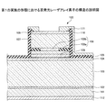
図1に示されるように、本実施の形態における面発光レーザアレイ素子には、基板101の上に、バッファ層102、下部半導体DBR103、下部スペーサ層104、活性層105、上部スペーサ層106、上部半導体DBR107、コンタクト層109、誘電体層110、上部電極111等が形成されており、基板101の裏面には下部電極112が形成されている。また、上部半導体DBR107には、電流狭窄層108が形成されており、電流狭窄層108は、メサ120の周辺部において選択酸化がなされている選択酸化領域108aと、中心部において酸化がされていない電流狭窄領域108bとを有している。尚、本実施の形態においては、下部半導体DBR103により下部DBRが形成されており、上部半導体DBR107により上部DBRが形成されているものとする。
As shown in FIG. 1, the surface emitting laser array element according to the present embodiment includes a
基板101は、n−GaAs基板により形成されており、バッファ層102は、基板101の上に形成されており、n−GaAs層により形成されている。
The
下部半導体DBR103は、バッファ層102の上に形成されており、発振波長をλとした場合、光学的厚さがλ/4となる膜厚のn−Al0.9Ga0.1Asからなる低屈折率層と、光学的厚さがλ/4となる膜厚のn−Al0.3Ga0.7Asからなる高屈折率層とをペアとするものが、n−Al0.9Ga0.1Asから始まり、40.5ペア積層形成されている。また、高屈折率層と低屈折率層との間には、電気抵抗を低減するため、一方の組成から他方の組成へ向かって組成を徐々に変化させた厚さ20nmの組成傾斜層が設けられている。尚、高屈折率層及び低屈折率層の膜厚には、いずれも隣接する組成傾斜層の1/2が含まれているものとする。また、光学的厚さがλ/4とは、その層における実際の厚さは、λ/4n(但し、nはその層の媒質の屈折率)である。
The
下部スペーサ層104は、下部半導体DBR103の上に形成されており、ノンドープのAl0.6Ga0.4Asにより形成されている。
The
活性層105は、下部スペーサ層104の上に形成されており、Al0.15Ga0.85As/Al0.3Ga0.7Asからなる3重量子井戸構造の活性層により形成されている。
The
上部スペーサ層106は、活性層105の上に形成されており、ノンドープのAl0.6Ga0.4Asにより形成されている。
The upper spacer layer 106 is formed on the
尚、下部スペーサ層104、活性層105及び上部スペーサ層106からなる部分は、共振器構造体とも呼ばれており、その厚さが1波長の光学的厚さとなるように形成されている。尚、活性層105は、高い誘導放出確率が得られるように、電界の定在波分布における腹に対応する位置となる共振器構造体の中央に設けられている。
The portion composed of the
上部半導体DBR107は、上部スペーサ層106の上に形成されており、p−Al0.9Ga0.1Asからなる低屈折率層と、p−Al0.3Ga0.7Asからなる高屈折率層とをペアとするものが、25ペア積層形成されている。また、高屈折率層と低屈折率層との間には、電気抵抗を低減するため、一方の組成から他方の組成へ向かって組成を徐々に変化させた組成傾斜層が設けられている。尚、高屈折率層及び低屈折率層の膜厚は、いずれも隣接する組成傾斜層の1/2を含み、光学的厚さがλ/4となるように形成されている。
The
また、上部半導体DBR107における低屈折率層の1つには、厚さ30nmのAlAsにより形成された電流狭窄層108が形成されている。この電流狭窄層108の挿入位置は、上部スペーサ層106から2ペア目の低屈折率層に相当する部分に形成されている。
In addition, a
コンタクト層109は、上部半導体DBR107の上に形成されており、p−GaAsにより形成されている。
The
尚、本実施の形態においては、このように基板101の上に複数の半導体層が積層されたものを、以下では、便宜上「半導体積層体」と記載する場合がある。また、本実施の形態においては、上部電極111と上部電極111に接続される配線が形成されるが、これらについては後述する。
In the present embodiment, a structure in which a plurality of semiconductor layers are stacked on the
(面発光レーザアレイ素子の製造方法)
次に、本実施の形態における面発光レーザアレイ素子の製造方法について説明する。
(Manufacturing method of surface emitting laser array element)
Next, a method for manufacturing the surface emitting laser array element in the present embodiment will be described.
最初に、基板101の上に、半導体積層体となるバッファ層102、下部半導体DBR103、下部スペーサ層104、活性層105、上部スペーサ層106、上部半導体DBR107、コンタクト層109を有機金属気相成長法(MOCVD:Metal Organic Chemical Vapor Deposition)法または、分子線エピタキシャル成長法(MBE:Molecular Beam Epitaxy)法による結晶成長により形成する。例えば、MOCVD法により形成する場合には、III族の原料としては、トリメチルアルミニウム(TMA)、トリメチルガリウム(TMG)、トリメチルインジウム(TMI)を用い、V族の原料としては、フォスフィン(PH3)、アルシン(AsH3)を用い、また、p型ドーパントの原料には四臭化炭素(CBr4)、ジメチルジンク(DMZn)を用い、n型ドーパントの原料にはセレン化水素(H2Se)を用いて上述した各層を成膜する。尚、各膜の膜厚や層数などについては、上述した通りである。
First, on the
次に、コンタクト層109の上にレジストパターンを形成する。このレジストパターンは、メサ120が形成される領域に形成されるものであり、1辺の長さが25μmの正方形状のレジストパターンであって、隣接するレジストパターン間の間隔が15μmとなるように、2次元的に形成する。
Next, a resist pattern is formed on the
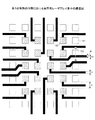
次に、ICP(Inductively Coupled Plasma)ドライエッチング法により、形成されたレジストパターンをマスクとして4角柱状のメサ120及びダミーメサ121を形成する。これにより、メサ120及びダミーメサ121の周囲における上部半導体DBR107は除去される。尚、形成されるメサ120及びダミーメサ121は、メサ120及びダミーメサ121の周囲において、ドライエッチングの終点が活性層105近傍となるように形成されており、上面が4角形となる4角柱状のメサ120及びダミーメサ121の高さは、約3.3μmである。図2は、この工程において形成されたメサ120及びダミーメサ121を上から見た図である。図2に示されるように、中央部分には、面発光レーザを形成するためのメサ120が、縦5列、横4列となるように、計20個形成されている。また、これらのメサ120の周囲を囲むように、外周部分には、ダミーメサ121が形成されている。この際、形成されるメサ120及びダミーメサ121は、一辺の長さLが25μmの正方形状のものであり、隣り合うメサ120同士の間隔Aが15μmとなるように形成されている。尚、本実施の形態においては、メサ120及びダミーメサ121は、略同一形状で形成されており、メサ120及びダミーメサ121は、2次元アレイ状に形成されているものとする。
Next, a quadrangular
次に、レジストパターンを有機溶剤等により除去する。 Next, the resist pattern is removed with an organic solvent or the like.
次に、メサ120が形成されているものを酸化処理する。具体的には、メサ120の側面において露出している電流狭窄層108をメサ120の周囲より選択酸化する。これにより、電流狭窄層108に含まれているAl(アルミニウム)が酸化され、メサ120の周辺部には選択酸化領域108aが形成される。この際、メサ120の中央部には、酸化されていない電流狭窄領域108bが形成される。このように形成された電流狭窄層108においては、酸化されている選択酸化領域108aには電流は流れることはなく、酸化されていない電流狭窄領域108bのみに電流が流れる。従って、流れる電流をメサ120の中央部の電流狭窄領域108bに絞り込むことができ、活性層105に絞り込まれた電流を流すことができる。
Next, the
次に、電流狭窄層108における選択酸化を行なった後、素子分離溝を形成する。具体的には、選択酸化を行なった後、フォトレジストを塗布し、露光装置による露光、現像を行なうことにより、素子分離溝が形成される領域に開口部を有するレジストパターンを形成する。この露光においては、露光装置としてコンタクト露光装置が用いられ、フォトレジストが塗布されている面に、フォトマスクを密着させて露光が行なわれる。この後、ICPエッチング等のドライエッチングにより、レジストパターンが形成されていない領域の半導体層等を除去することにより、素子分離溝を形成する。この後、レジストパターンは有機溶剤等により除去する。
Next, after selective oxidation in the
次に、気相化学堆積法(CVD法)を用いて、誘電体層110を形成する。この誘電体層110は、SiN、SiONまたは、SiO2により形成されている。この誘電体層110は保護膜となるものであり、本実施の形態においては、単に、保護膜と記載する場合がある。
Next, the
次に、メサ120の上面における誘電体層110の一部を除去する。具体的には、誘電体層110の上にフォトレジストを塗布した後、露光装置による露光、現像を行なうことにより、メサ120の上面に開口部を有するレジストパターンを形成する。この露光には、露光装置としてコンタクト露光装置が用いられており、フォトレジストが塗布されている面にフォトマスクを密着させて露光が行なわれる。この後、BHFにより、レジストパターンの開口部において露出している誘電体層110を除去し、コンタクト層109の表面を露出させる。尚、この工程においては、素子分離溝に形成されている誘電体膜110も同時に除去される。
Next, a part of the
次に、図4に示されるように、p側電極となる上部電極111及び配線130を形成する。具体的には、誘電体層110の上に、フォトレジストを塗布し、露光装置による露光、現像を行なうことにより、上部電極111及び配線130が形成される領域に開口部を有するレジストパターンを形成する。この露光には、露光装置として水銀ランプを用いたコンタクト露光装置が用いられ、フォトレジストが塗布されている面にフォトマスクを密着させて露光が行なわれる。このようにして形成されるレジストパターンは、上部電極111が形成される領域及び配線130が形成される領域に開口部を有するものであり、この開口部には、ダミーメサ121の上面から、ダミーメサ121の側面、ダミーメサ121の周囲の底面にわたり、幅が7.0μmとなる配線130を形成するための領域も含まれている。
Next, as shown in FIG. 4, the
次に、p側電極となる上部電極111及び配線130を形成するため、真空蒸着により金属膜を成膜する。本実施の形態では、上部電極111及び配線130を形成するための金属膜としては、Ti/Pt/Auからなる金属多層膜を用いている。
Next, in order to form the
次に、有機溶剤等に浸漬させることにより、レジストパターンの上に成膜された金属膜をレジストパターンとともに、リフトオフにより除去する。これにより、p側電極となる上部電極111及び配線130を形成することができる。
Next, the metal film formed on the resist pattern is removed together with the resist pattern by lift-off by being immersed in an organic solvent or the like. Thereby, the
ところで、図3に示される従来のもののように、メサ120等の間隔Aを15μmとし、メサ120等とメサ120等との間に配線930aを形成する場合、コンタクト露光では、メサ120等とメサ120等との間においては、上部半導体DBR107等が除去されているため、フォトマスクとメサ120等の周囲の底面との距離が離れている。このため、この部分に微細な配線を形成しようとすればする程、露光により形成される像がぼけてしまい、配線930aを所望の幅Bの線幅で形成することが困難となる。また、形成される配線の幅がBである場合、メサ120等の間隔Aは幅Bよりも狭くすることができない。このため、面発光レーザの高集積化のためメサ120等の間隔Aを狭くした場合には、図3に示されるように、ダミーメサ121の上面を通るように、具体的には、ダミーメサ121のを越えて、即ち、ダミーメサ121の側面、上面、側面を通るような配線930bを形成する必要がある。しかしながら、このような配線は、前述したように、ダミーメサ121の上面の端部において断線が生じる可能性があるため、好ましくはない。
By the way, when the distance A between the
そこで、本実施の形態においては、図4及び図5に示されるように、ダミーメサ121の近傍の配線130を、ダミーメサ121の上面から、ダミーメサ121の側面、ダミーメサ121の周囲の底面にわたり形成する。具体的には、ダミーメサ121の近傍の配線130を、ダミーメサ121の上面から、ダミーメサ121の側面、ダミーメサ121の配線長手方向、即ち、電流が流れる方向の周囲の底面にわたり形成する。このように形成される配線130は、メサ120等の間隔Aを狭くして高集積化させた場合においても、形成可能であるため、面発光レーザの高集積化を妨げることはない。また、ダミーメサ121の間に、2本の配線を形成することにより、更に、集積度を高くすることが可能となる。
Therefore, in the present embodiment, as shown in FIGS. 4 and 5, the
本実施の形態では、配線130は、幅Bが7.0μmとなるように形成されており、ダミーメサ121の上面を通る領域の幅B1が3.0μm、ダミーメサ121の周囲の底面を通る領域の幅B2が4.0μmとなるように形成されている。この際、B1<B2となるように形成されていることが好ましい。これにより、メサ120等の間隔Aを狭めても、配線130の一部をダミーメサ121の周囲の底面を通る領域に、形成することができるため、断線等の発生を防ぐことができる。
In the present embodiment, the
尚、図5は、図4における一点鎖線4A−4Bにおいて切断した断面図を示す。また、形成されるダミーメサ121の高さHは、3.3μmであり、メサ120の高さもこの高さと同じである。また、配線130の幅Bは、ダミーメサ121の上面を通る領域の幅B1と、ダミーメサ121の周囲の底面を通る領域の幅B2と、ダミーメサ121の側面を通る領域の幅B3との和となるものであるが、幅B3は、幅B1及び幅B2と比較して狭いため、図4等においては省略されているものとする。
FIG. 5 shows a cross-sectional view taken along the alternate long and
更に、図6に示されるように、配線130のうち、ダミーメサ121の周囲の底面にわたり形成されている配線の領域130aの幅を、ダミーメサ121の周囲に広がる方向に、他の領域よりも広く形成してもよい。これにより、例えば、配線130をフォトリソグラフィー工程により形成する際に、位置合わせにおいてズレが生じた場合であっても、断線のリスクを低くすることができる。具体的には、フォトリソグラフィー工程の位置合わせ精度の分だけ、配線130における配線の領域130aの幅を広くすることにより、位置合わせにおけるズレによる断線のリスクを抑制することが可能となる。
Further, as shown in FIG. 6, in the
次に、基板101の裏側を所定の厚さ(例えば100μm程度)まで研磨した後、n側電極となる下部電極112を形成する。本実施の形態では、n側電極となる下部電極112は、AuGe/Ni/Auからなる多層膜により形成されている。
Next, after the back side of the
次に、アニールを行なうことにより、p側電極となる上部電極111とn側電極となる下部電極112においてオーミックコンタクトをとる。これにより、メサ120の形成されている領域には面発光レーザが各々形成される。
Next, an ohmic contact is made between the
この後、スクライブ・ブレーキングにより、チップ毎に切断し、この後、種々の後工程を経て、本実施の形態における面発光レーザアレイ素子を作製することができる。上述した製造方法により、本実施の形態における面発光レーザアレイ素子を3000個製造したところ、すべての面発光レーザアレイ素子において、発光が確認され、出力特性測定の結果、配線130における断線が発生していないことが確認された。
Thereafter, the surface-emitting laser array element according to the present embodiment can be manufactured by cutting each chip by scribing and breaking, and thereafter performing various post-processes. When 3000 surface-emitting laser array elements in the present embodiment were manufactured by the above-described manufacturing method, light emission was confirmed in all the surface-emitting laser array elements, and as a result of output characteristic measurement, disconnection in the
〔第2の実施の形態〕
次に、第2の実施の形態について説明する。本実施の形態は、第1の実施の形態における面発光レーザアレイ素子を用いた光走査装置及び画像形成装置であるレーザプリンタ1000である。
[Second Embodiment]
Next, a second embodiment will be described. This embodiment is a
図7に基づき、本実施の形態におけるレーザプリンタ1000について説明する。本実施の形態におけるレーザプリンタ1000は、光走査装置1010、感光体ドラム1030、帯電チャージャ1031、現像ローラ1032、転写チャージャ1033、除電ユニット1034、クリーニングユニット1035、トナーカートリッジ1036、給紙コロ1037、給紙トレイ1038、レジストローラ対1039、定着ローラ1041、排紙ローラ1042、排紙トレイ1043、通信制御装置1050、及び上記各部を統括的に制御するプリンタ制御装置1060等を備えている。尚、これらは、プリンタ筐体1044の中の所定位置に収容されている。
Based on FIG. 7, the
通信制御装置1050は、ネットワークなどを介した上位装置(例えばパソコン)との双方向の通信を制御する。
The
感光体ドラム1030は、円柱状の部材であり、その表面には感光層が形成されている。すなわち、感光体ドラム1030の表面が被走査面である。そして、感光体ドラム1030は、矢印Xで示す方向に回転するようになっている。
The
帯電チャージャ1031、現像ローラ1032、転写チャージャ1033、除電ユニット1034及びクリーニングユニット1035は、それぞれ感光体ドラム1030の表面近傍に配置されている。そして、感光体ドラム1030の回転方向に沿って、帯電チャージャ1031→現像ローラ1032→転写チャージャ1033→除電ユニット1034→クリーニングユニット1035の順に配置されている。
The charging
帯電チャージャ1031は、感光体ドラム1030の表面を均一に帯電させる。
The charging
光走査装置1010は、帯電チャージャ1031で帯電された感光体ドラム1030の表面を、上位装置からの画像情報に基づいて変調された光束により走査し、感光体ドラム1030の表面に画像情報に対応した潜像を形成する。ここで形成された潜像は、感光体ドラム1030の回転に伴って現像ローラ1032の方向に移動する。なお、この光走査装置1010の構成については後述する。
The
トナーカートリッジ1036にはトナーが格納されており、このトナーは現像ローラ1032に供給される。
Toner cartridge 1036 stores toner, and this toner is supplied to developing
現像ローラ1032は、感光体ドラム1030の表面に形成された潜像にトナーカートリッジ1036から供給されたトナーを付着させて画像情報を顕像化させる。ここでトナーが付着した潜像(以下では、便宜上「トナー像」ともいう)は、感光体ドラム1030の回転に伴って転写チャージャ1033の方向に移動する。
The developing
給紙トレイ1038には記録紙1040が格納されている。この給紙トレイ1038の近傍には給紙コロ1037が配置されており、この給紙コロ1037は、記録紙1040を給紙トレイ1038から1枚づつ取り出し、レジストローラ対1039に搬送する。このレジストローラ対1039は、給紙コロ1037によって取り出された記録紙1040を一旦保持するとともに、この記録紙1040を感光体ドラム1030の回転に合わせて感光体ドラム1030と転写チャージャ1033との間隙に向けて送り出す。
転写チャージャ1033には、感光体ドラム1030の表面のトナーを電気的に記録紙1040に引きつけるために、トナーとは逆極性の電圧が印加されている。この電圧により、感光体ドラム1030の表面のトナー像が記録紙1040に転写される。ここで転写された記録紙1040は、定着ローラ1041に送られる。
A voltage having a polarity opposite to that of the toner is applied to the
定着ローラ1041では、熱と圧力とが記録紙1040に加えられ、これによってトナーが記録紙1040上に定着される。ここで定着された記録紙1040は、排紙ローラ1042を介して排紙トレイ1043に送られ、排紙トレイ1043上に順次スタックされる。
In the fixing
除電ユニット1034は、感光体ドラム1030の表面を除電する。
The
クリーニングユニット1035は、感光体ドラム1030の表面に残ったトナー(残留トナー)を除去する。残留トナーが除去された感光体ドラム1030の表面は、再度帯電チャージャ1031に対向する位置に戻る。
The
次に、図8に基づき光走査装置1010について説明する。光走査装置1010は、光源ユニット1100、不図示のカップリングレンズ及び開口板、シリンドリカルレンズ1113、ポリゴンミラー1114、fθレンズ1115、トロイダルレンズ1116、2つのミラー(1117、1118)、及び上記各部を統括的に制御する不図示の制御装置を備えている。尚、光源ユニット1100には、第1の実施の形態における面発光レーザアレイ素子を含むものにより形成されている。
Next, the
シリンドリカルレンズ1113は、光源ユニット1100から出力された光を、ミラー1117を介してポリゴンミラー1114の偏向反射面近傍に集光する。
The
ポリゴンミラー1114は、高さの低い正六角柱状部材からなり、側面には6面の偏向反射面が形成されている。 そして、不図示の回転機構により、矢印Yに示す方向に一定の角速度で回転されている。
The
従って、光源ユニット1100から出射され、シリンドリカルレンズ1113によってポリゴンミラー1114の偏向反射面近傍に集光された光は、ポリゴンミラー1114の回転により一定の角速度で偏向される。
Accordingly, the light emitted from the
fθレンズ1115は、ポリゴンミラー1114からの光の入射角に比例した像高をもち、ポリゴンミラー1114により一定の角速度で偏向される光の像面を、主走査方向に関して等速移動させる。 トロイダルレンズ1116は、fθレンズ1115からの光をミラー1118を介して、感光体ドラム1030の表面に結像する。
The
トロイダルレンズ1116は、fθレンズ1115を介した光束の光路上に配置されている。そして、このトロイダルレンズ1116を介した光束が、感光体ドラム1030の表面に照射され、光スポットが形成される。この光スポットは、ポリゴンミラー1114の回転に伴って感光体ドラム1030の長手方向に移動する。すなわち、感光体ドラム1030上を走査する。このときの光スポットの移動方向が「主走査方向」である。また、感光体ドラム1030の回転方向が「副走査方向」である。
The
ポリゴンミラー1114と感光体ドラム1030との間の光路上に配置される光学系は、走査光学系とも呼ばれている。本実施の形態では、走査光学系は、fθレンズ1115とトロイダルレンズ1116とから構成されている。なお、fθレンズ1115とトロイダルレンズ1116の間の光路上、及びトロイダルレンズ1116と感光体ドラム1030の間の光路上の少なくとも一方に、少なくとも1つの折り返しミラーが配置されてもよい。
The optical system arranged on the optical path between the
この場合に、面発光レーザアレイLAが、図9に示されるように配置されていると、面発光レーザアレイLAでは、各面発光レーザ素子(VCSEL)の中心から副走査方向に対応する方向に垂線を下ろした時の副走査方向に対応する方向における各面発光レーザ素子の位置関係が等間隔(間隔d2とする)となるので、点灯のタイミングを調整することで感光体ドラム1030上では副走査方向に等間隔で光源が並んでいる場合と同様な構成と捉えることができる。例えば、副走査方向に対応した方向に関する面発光レーザ素子のピッチd1が26.5μmであれば、前記間隔d2は2.65μmとなる。そして、光学系の倍率を2倍とすれば、感光体ドラム1030上では副走査方向に5.3μm間隔で書き込みドットを形成することができる。これは、4800dpi(ドット/インチ)に対応している。すなわち、4800dpi(ドット/インチ)の高密度書込みができる。もちろん、主走査方向に対応する方向の面発光レーザ数を増加したり、前記ピッチd1を狭くして間隔d2を更に小さくするアレイ配置としたり、光学系の倍率を下げる等を行えばより高密度化でき、より高品質の印刷が可能となる。なお、主走査方向の書き込み間隔は、光源の点灯のタイミングで容易に制御できる。
In this case, if the surface emitting laser array LA is arranged as shown in FIG. 9, in the surface emitting laser array LA, the center of each surface emitting laser element (VCSEL) extends in the direction corresponding to the sub-scanning direction. Since the positional relationship of the surface emitting laser elements in the direction corresponding to the sub-scanning direction when the vertical line is lowered is equal (interval d2), the lighting timing is adjusted to adjust the sub-scanning on the
また、この場合には、レーザプリンタ1000では書きこみドット密度が上昇しても面発光レーザ素子は高い単一基本横モード出力を発生させる事ができるので、印刷速度を落とすことなく印刷することができる。また、同じ書きこみドット密度の場合には印刷速度を更に速くすることができる。
Further, in this case, in the
尚、本実施の形態における説明では、画像形成装置としてレーザプリンタ1000の場合について説明したが、これに限定されるものではない。
In the description of the present embodiment, the case of the
例えば、レーザ光によって発色する媒体(例えば、用紙)に直接、レーザ光を照射する画像形成装置であってもよい。 For example, an image forming apparatus that directly irradiates laser light onto a medium (for example, paper) that develops color with laser light may be used.
また、像担持体として銀塩フィルムを用いた画像形成装置であっても良い。この場合には、光走査により銀塩フィルム上に潜像が形成され、この潜像は通常の銀塩写真プロセスにおける現像処理と同等の処理で可視化することができる。そして、通常の銀塩写真プロセスにおける焼付け処理と同等の処理で印画紙に転写することができる。このような画像形成装置は光製版装置や、CTスキャン画像等を描画する光描画装置として実施できる。 Further, an image forming apparatus using a silver salt film as the image carrier may be used. In this case, a latent image is formed on the silver salt film by optical scanning, and this latent image can be visualized by a process equivalent to a developing process in a normal silver salt photographic process. Then, it can be transferred to photographic paper by a process equivalent to a printing process in a normal silver salt photographic process. Such an image forming apparatus can be implemented as an optical plate making apparatus or an optical drawing apparatus that draws a CT scan image or the like.
本実施の形態における光走査装置1010では、第1の実施の形態における面発光レーザアレイ素子を用いているため、高品質な潜像を安定して形成することができる。また、本実施の形態におけるレーザプリンタ1000では、第1の実施の形態における面発光レーザアレイ素子を用いているため、高品質な画像を安定して形成することができる。
Since the
〔第3の実施の形態〕
次に、第3の実施の形態について説明する。第3の実施の形態は、複数の感光体ドラムを備えるカラープリンタ2000である。
[Third Embodiment]
Next, a third embodiment will be described. The third embodiment is a
図10に基づき、本実施の形態におけるカラープリンタ2000について説明する。本実施の形態におけるカラープリンタ2000は、4色(ブラック、シアン、マゼンタ、イエロー)を重ね合わせてフルカラーの画像を形成するタンデム方式の多色カラープリンタであり、ブラック用の「感光体ドラムK1、帯電装置K2、現像装置K4、クリーニングユニットK5、及び転写装置K6」と、シアン用の「感光体ドラムC1、帯電装置C2、現像装置C4、クリーニングユニットC5、及び転写装置C6」と、マゼンタ用の「感光体ドラムM1、帯電装置M2、現像装置M4、クリーニングユニットM5、及び転写装置M6」と、イエロー用の「感光体ドラムY1、帯電装置Y2、現像装置Y4、クリーニングユニットY5、及び転写装置Y6」と、光走査装置2010と、転写ベルト2080と、定着ユニット2030などを備えている。
Based on FIG. 10, the
各感光体ドラムは、図10において示される矢印の方向に回転し、各感光体ドラムの周囲には、回転順にそれぞれ帯電装置、現像装置、転写装置、クリーニングユニットが配置されている。各帯電装置は、対応する感光体ドラムの表面を均一に帯電する。帯電装置によって帯電された各感光体ドラム表面に光走査装置2010により光が照射され、各感光体ドラムに潜像が形成されるようになっている。そして、対応する現像装置により各感光体ドラム表面にトナー像が形成される。さらに、対応する転写装置により、転写ベルト2080上の記録紙に各色のトナー像が転写され、最終的に定着ユニット2030により記録紙に画像が定着される。
Each photosensitive drum rotates in the direction of the arrow shown in FIG. 10, and a charging device, a developing device, a transfer device, and a cleaning unit are arranged around each photosensitive drum in the order of rotation. Each charging device uniformly charges the surface of the corresponding photosensitive drum. The surface of each photoconductive drum charged by the charging device is irradiated with light by the
光走査装置2010は、第1の実施の形態における面発光レーザアレイ素子を含む光源ユニットを、各々の色毎に有しており、第2の実施の形態において説明した光走査装置1010と同様の効果を得ることができる。また、カラープリンタ2000は、この光走査装置2010を備えているため、第2の実施の形態におけるレーザプリンタ1000と同様の効果を得ることができる。
The
以上、本発明の実施に係る形態について説明したが、上記内容は、発明の内容を限定するものではない。 As mentioned above, although the form which concerns on implementation of this invention was demonstrated, the said content does not limit the content of invention.
101 基板
102 バッファ層
103 下部半導体DBR
104 下部スペーサ層
105 活性層
106 上部スペーサ層
107 上部半導体DBR
108 電流狭窄層
108a 選択酸化領域
108b 電流狭窄領域
109 コンタクト層
110 保護膜
111 上部電極
112 下部電極
120 メサ
121 ダミーメサ
130 配線
1000 レーザプリンタ(画像形成装置)
1010 光走査装置
2000 カラープリンタ(画像形成装置)
101
104
108
1010
Claims (9)
前記複数のメサは、配線が接続される電極を有し、
前記配線の一部は、前記ダミーメサの上面及び側面と該ダミーメサの周囲の底面にわたり形成されているものであって、
前記配線における前記ダミーメサの周囲の底面にわたり形成されている配線の領域において、
前記配線の領域における配線の幅が、前記ダミーメサの周囲に広がる方向に、他の領域よりも広く形成されていることを特徴とする面発光レーザアレイ素子。 A surface-emitting laser element having a plurality of mesas and a plurality of dummy mesas located around the plurality of mesas,
The plurality of mesas have electrodes to which wiring is connected,
Part of the wire, it der those formed over the bottom surface of the periphery of the upper and side surfaces and said Damimesa the Damimesa,
In the wiring region formed over the bottom surface around the dummy mesa in the wiring,
Width of the wiring in the area of the wiring, the direction extending around the Damimesa, another surface emitting laser element array according to claim that you have been wider than the region.
請求項1から7のいずれかに記載の面発光レーザアレイ素子を有する光源と、
前記光源からの光を偏向する光偏向部と、
前記光偏向部により偏向された光を前記被走査面上に集光する走査光学系と、
を有することを特徴とする光走査装置。 An optical scanning device that scans a surface to be scanned with light,
A light source having a surface emitting laser element array according to any one of claims 1 to 7,
A light deflector for deflecting light from the light source;
A scanning optical system for condensing the light deflected by the light deflection unit on the surface to be scanned;
An optical scanning device comprising:
前記像担持体に対して画像情報に応じて変調された光を走査する請求項8に記載の光走査装置と、
を有することを特徴とする画像形成装置。 An image carrier;
The optical scanning device according to claim 8 , wherein the image carrier is scanned with light modulated according to image information;
An image forming apparatus comprising:
Priority Applications (2)
| Application Number | Priority Date | Filing Date | Title |
|---|---|---|---|
| JP2012260156A JP6085956B2 (en) | 2012-03-09 | 2012-11-28 | Surface emitting laser array element, optical scanning device, and image forming apparatus |
| US13/781,975 US8879600B2 (en) | 2012-03-09 | 2013-03-01 | Surface emitting laser array element, optical scanning device, and image forming apparatus |
Applications Claiming Priority (3)
| Application Number | Priority Date | Filing Date | Title |
|---|---|---|---|
| JP2012052689 | 2012-03-09 | ||
| JP2012052689 | 2012-03-09 | ||
| JP2012260156A JP6085956B2 (en) | 2012-03-09 | 2012-11-28 | Surface emitting laser array element, optical scanning device, and image forming apparatus |
Publications (3)
| Publication Number | Publication Date |
|---|---|
| JP2013214706A JP2013214706A (en) | 2013-10-17 |
| JP2013214706A5 JP2013214706A5 (en) | 2016-01-07 |
| JP6085956B2 true JP6085956B2 (en) | 2017-03-01 |
Family
ID=49211915
Family Applications (1)
| Application Number | Title | Priority Date | Filing Date |
|---|---|---|---|
| JP2012260156A Active JP6085956B2 (en) | 2012-03-09 | 2012-11-28 | Surface emitting laser array element, optical scanning device, and image forming apparatus |
Country Status (2)
| Country | Link |
|---|---|
| US (1) | US8879600B2 (en) |
| JP (1) | JP6085956B2 (en) |
Families Citing this family (5)
| Publication number | Priority date | Publication date | Assignee | Title |
|---|---|---|---|---|
| JP2016174136A (en) | 2015-03-16 | 2016-09-29 | 株式会社リコー | Surface-emitting laser array, laser apparatus, ignition device and internal combustion engine |
| JP2017103448A (en) | 2015-11-24 | 2017-06-08 | 株式会社リコー | Laser light generating apparatus, laser processing machine and manufacturing method of work piece |
| JP2018181912A (en) * | 2017-04-04 | 2018-11-15 | 住友電気工業株式会社 | Method for fabricating surface emission laser |
| JP7367484B2 (en) | 2019-11-22 | 2023-10-24 | 株式会社リコー | Surface-emitting laser elements, surface-emitting lasers, surface-emitting laser devices, light source devices, and detection devices |
| WO2023233850A1 (en) * | 2022-05-30 | 2023-12-07 | ソニーセミコンダクタソリューションズ株式会社 | Surface light emitting element |
Family Cites Families (16)
| Publication number | Priority date | Publication date | Assignee | Title |
|---|---|---|---|---|
| JP2005191343A (en) | 2003-12-26 | 2005-07-14 | Ricoh Co Ltd | Vertical cavity surface emitting laser, manufacturing method thereof, and optical transmission system |
| JP4752201B2 (en) | 2004-06-29 | 2011-08-17 | 富士ゼロックス株式会社 | Surface emitting semiconductor laser device and manufacturing method thereof |
| JP4969066B2 (en) * | 2005-07-15 | 2012-07-04 | 株式会社リコー | Surface emitting semiconductor laser array |
| WO2007126159A1 (en) | 2006-04-28 | 2007-11-08 | Ricoh Company, Ltd. | Surface-emission laser array, optical scanning apparatus and image forming apparatus |
| JP5087874B2 (en) | 2006-07-28 | 2012-12-05 | 富士ゼロックス株式会社 | Surface emitting semiconductor laser and manufacturing method thereof |
| KR100990702B1 (en) | 2006-08-23 | 2010-10-29 | 가부시키가이샤 리코 | Surface-emitting laser array, optical scanning device, and image forming device |
| US7924487B2 (en) * | 2007-02-09 | 2011-04-12 | Ricoh Company, Ltd. | Optical scanning device and image forming apparatus |
| JP5748949B2 (en) | 2008-11-20 | 2015-07-15 | 株式会社リコー | Surface emitting laser element, surface emitting laser array, optical scanning device, and image forming apparatus |
| JP5504784B2 (en) | 2009-03-18 | 2014-05-28 | 株式会社リコー | Surface emitting laser, surface emitting laser array, optical scanning device, and image forming apparatus |
| JP5515767B2 (en) | 2009-05-28 | 2014-06-11 | 株式会社リコー | Surface emitting laser element manufacturing method, surface emitting laser element, surface emitting laser array, optical scanning apparatus, and image forming apparatus |
| JP5532239B2 (en) | 2009-11-26 | 2014-06-25 | 株式会社リコー | Surface emitting laser element, surface emitting laser array, optical scanning device, and image forming apparatus |
| JP2011148957A (en) | 2010-01-25 | 2011-08-04 | Kyocera Chemical Corp | Water-soluble resin composition and water-based coating using the same |
| JP2011222721A (en) * | 2010-04-08 | 2011-11-04 | Sony Corp | Semiconductor laser |
| JP5585940B2 (en) | 2010-04-22 | 2014-09-10 | 株式会社リコー | Surface emitting laser element, surface emitting laser array, optical scanning device, image forming apparatus, and method for manufacturing surface emitting laser element |
| JP5721055B2 (en) | 2010-06-11 | 2015-05-20 | 株式会社リコー | Surface emitting laser element, surface emitting laser array, optical scanning device, image forming apparatus, and method for manufacturing surface emitting laser element |
| US8416821B2 (en) * | 2010-06-11 | 2013-04-09 | Ricoh Company, Ltd. | Surface emitting laser element, surface emitting laser array, optical scanning unit, image forming apparatus and method of manufacturing surface emitting laser element |
-
2012
- 2012-11-28 JP JP2012260156A patent/JP6085956B2/en active Active
-
2013
- 2013-03-01 US US13/781,975 patent/US8879600B2/en active Active
Also Published As
| Publication number | Publication date |
|---|---|
| US20130251408A1 (en) | 2013-09-26 |
| JP2013214706A (en) | 2013-10-17 |
| US8879600B2 (en) | 2014-11-04 |
Similar Documents
| Publication | Publication Date | Title |
|---|---|---|
| JP5261754B2 (en) | Surface emitting laser element, surface emitting laser array, optical scanning device, and image forming apparatus | |
| JP5316783B2 (en) | Surface emitting laser element, surface emitting laser array, optical scanning device, and image forming apparatus | |
| JP5532321B2 (en) | Surface emitting laser element, surface emitting laser array, optical scanning device, and image forming apparatus | |
| JP5316784B2 (en) | Surface emitting laser element, surface emitting laser array, optical scanning device, and image forming apparatus | |
| JP4890358B2 (en) | Surface emitting laser array, optical scanning device, image forming apparatus, optical transmission module, and optical transmission system | |
| JP5522595B2 (en) | Surface emitting laser element, surface emitting laser array, optical scanning device, and image forming apparatus | |
| JP2011009693A (en) | Method of manufacturing surface emitting laser element, surface emitting laser element, surface emitting laser array, optical scanning device, and image forming apparatus | |
| JP6085956B2 (en) | Surface emitting laser array element, optical scanning device, and image forming apparatus | |
| JP5531584B2 (en) | Surface emitting laser manufacturing method, surface emitting laser, surface emitting laser array element, optical scanning device, and image forming apparatus | |
| JP2011181786A (en) | Surface emitting laser element, surface emitting laser array, optical scanner, and image forming apparatus | |
| JP6015982B2 (en) | Surface emitting laser, optical scanning device, and image forming apparatus | |
| JP5505614B2 (en) | Surface emitting laser element, surface emitting laser array, optical scanning device, and image forming apparatus | |
| JP2010283083A (en) | Surface emitting semiconductor laser, method for manufacturing surface emitting semiconductor laser, surface emitting laser array element, optical scanning device and image forming apparatus | |
| JP2014096515A (en) | Surface emitting laser element, surface emitting laser array, optical scanning device, image formation device and surface emitting laser element manufacturing method | |
| JP2012015364A (en) | Method of manufacturing surface-emitting laser element, surface-emitting laser element, surface-emitting laser array element, optical scanner, and image forming device | |
| JP5843178B2 (en) | Surface emitting laser element, surface emitting laser array, optical scanning device, and image forming apparatus | |
| JP5911003B2 (en) | Surface emitting laser element, surface emitting laser array, optical scanning device, and image forming apparatus | |
| JP5850075B2 (en) | Manufacturing method of surface emitting laser element | |
| JP5054622B2 (en) | Surface emitting laser array, optical scanning device, and image forming apparatus | |
| JP2013051277A (en) | Surface emitting laser, surface emitting laser array, optical scanner and image formation apparatus | |
| JP2015111634A (en) | Surface emission laser array, optical scanner, and image forming apparatus | |
| JP2013175613A (en) | Surface light emission laser element, surface light emission laser array, optical scanner, and image formation device | |
| JP2013182965A (en) | Manufacturing method, surface light-emitting laser element, surface light-emitting laser array, optical scanner, and image forming apparatus |
Legal Events
| Date | Code | Title | Description |
|---|---|---|---|
| A521 | Request for written amendment filed |
Free format text: JAPANESE INTERMEDIATE CODE: A523 Effective date: 20151112 |
|
| A621 | Written request for application examination |
Free format text: JAPANESE INTERMEDIATE CODE: A621 Effective date: 20151112 |
|
| A977 | Report on retrieval |
Free format text: JAPANESE INTERMEDIATE CODE: A971007 Effective date: 20160629 |
|
| A131 | Notification of reasons for refusal |
Free format text: JAPANESE INTERMEDIATE CODE: A131 Effective date: 20160726 |
|
| A521 | Request for written amendment filed |
Free format text: JAPANESE INTERMEDIATE CODE: A523 Effective date: 20160909 |
|
| TRDD | Decision of grant or rejection written | ||
| A01 | Written decision to grant a patent or to grant a registration (utility model) |
Free format text: JAPANESE INTERMEDIATE CODE: A01 Effective date: 20170104 |
|
| A61 | First payment of annual fees (during grant procedure) |
Free format text: JAPANESE INTERMEDIATE CODE: A61 Effective date: 20170117 |
|
| R151 | Written notification of patent or utility model registration |
Ref document number: 6085956 Country of ref document: JP Free format text: JAPANESE INTERMEDIATE CODE: R151 |