JP6082284B2 - Wiring board and manufacturing method thereof - Google Patents
Wiring board and manufacturing method thereof Download PDFInfo
- Publication number
- JP6082284B2 JP6082284B2 JP2013051537A JP2013051537A JP6082284B2 JP 6082284 B2 JP6082284 B2 JP 6082284B2 JP 2013051537 A JP2013051537 A JP 2013051537A JP 2013051537 A JP2013051537 A JP 2013051537A JP 6082284 B2 JP6082284 B2 JP 6082284B2
- Authority
- JP
- Japan
- Prior art keywords
- metal layer
- aluminum oxide
- oxide substrate
- connection pad
- wiring board
- Prior art date
- Legal status (The legal status is an assumption and is not a legal conclusion. Google has not performed a legal analysis and makes no representation as to the accuracy of the status listed.)
- Active
Links
Images


Classifications
-
- H—ELECTRICITY
- H05—ELECTRIC TECHNIQUES NOT OTHERWISE PROVIDED FOR
- H05K—PRINTED CIRCUITS; CASINGS OR CONSTRUCTIONAL DETAILS OF ELECTRIC APPARATUS; MANUFACTURE OF ASSEMBLAGES OF ELECTRICAL COMPONENTS
- H05K1/00—Printed circuits
- H05K1/02—Details
- H05K1/11—Printed elements for providing electric connections to or between printed circuits
- H05K1/111—Pads for surface mounting, e.g. lay-out
- H05K1/112—Pads for surface mounting, e.g. lay-out directly combined with via connections
-
- H—ELECTRICITY
- H01—ELECTRIC ELEMENTS
- H01L—SEMICONDUCTOR DEVICES NOT COVERED BY CLASS H10
- H01L21/00—Processes or apparatus adapted for the manufacture or treatment of semiconductor or solid state devices or of parts thereof
- H01L21/02—Manufacture or treatment of semiconductor devices or of parts thereof
- H01L21/04—Manufacture or treatment of semiconductor devices or of parts thereof the devices having at least one potential-jump barrier or surface barrier, e.g. PN junction, depletion layer or carrier concentration layer
- H01L21/48—Manufacture or treatment of parts, e.g. containers, prior to assembly of the devices, using processes not provided for in a single one of the subgroups H01L21/06 - H01L21/326
- H01L21/4814—Conductive parts
- H01L21/4846—Leads on or in insulating or insulated substrates, e.g. metallisation
- H01L21/486—Via connections through the substrate with or without pins
-
- H—ELECTRICITY
- H01—ELECTRIC ELEMENTS
- H01L—SEMICONDUCTOR DEVICES NOT COVERED BY CLASS H10
- H01L23/00—Details of semiconductor or other solid state devices
- H01L23/12—Mountings, e.g. non-detachable insulating substrates
- H01L23/14—Mountings, e.g. non-detachable insulating substrates characterised by the material or its electrical properties
- H01L23/142—Metallic substrates having insulating layers
-
- H—ELECTRICITY
- H01—ELECTRIC ELEMENTS
- H01L—SEMICONDUCTOR DEVICES NOT COVERED BY CLASS H10
- H01L23/00—Details of semiconductor or other solid state devices
- H01L23/48—Arrangements for conducting electric current to or from the solid state body in operation, e.g. leads, terminal arrangements ; Selection of materials therefor
- H01L23/488—Arrangements for conducting electric current to or from the solid state body in operation, e.g. leads, terminal arrangements ; Selection of materials therefor consisting of soldered or bonded constructions
- H01L23/498—Leads, i.e. metallisations or lead-frames on insulating substrates, e.g. chip carriers
- H01L23/49827—Via connections through the substrates, e.g. pins going through the substrate, coaxial cables
-
- H—ELECTRICITY
- H05—ELECTRIC TECHNIQUES NOT OTHERWISE PROVIDED FOR
- H05K—PRINTED CIRCUITS; CASINGS OR CONSTRUCTIONAL DETAILS OF ELECTRIC APPARATUS; MANUFACTURE OF ASSEMBLAGES OF ELECTRICAL COMPONENTS
- H05K3/00—Apparatus or processes for manufacturing printed circuits
- H05K3/40—Forming printed elements for providing electric connections to or between printed circuits
- H05K3/4038—Through-connections; Vertical interconnect access [VIA] connections
-
- H—ELECTRICITY
- H01—ELECTRIC ELEMENTS
- H01L—SEMICONDUCTOR DEVICES NOT COVERED BY CLASS H10
- H01L2224/00—Indexing scheme for arrangements for connecting or disconnecting semiconductor or solid-state bodies and methods related thereto as covered by H01L24/00
- H01L2224/01—Means for bonding being attached to, or being formed on, the surface to be connected, e.g. chip-to-package, die-attach, "first-level" interconnects; Manufacturing methods related thereto
- H01L2224/10—Bump connectors; Manufacturing methods related thereto
- H01L2224/15—Structure, shape, material or disposition of the bump connectors after the connecting process
- H01L2224/16—Structure, shape, material or disposition of the bump connectors after the connecting process of an individual bump connector
- H01L2224/161—Disposition
- H01L2224/16151—Disposition the bump connector connecting between a semiconductor or solid-state body and an item not being a semiconductor or solid-state body, e.g. chip-to-substrate, chip-to-passive
- H01L2224/16221—Disposition the bump connector connecting between a semiconductor or solid-state body and an item not being a semiconductor or solid-state body, e.g. chip-to-substrate, chip-to-passive the body and the item being stacked
- H01L2224/16225—Disposition the bump connector connecting between a semiconductor or solid-state body and an item not being a semiconductor or solid-state body, e.g. chip-to-substrate, chip-to-passive the body and the item being stacked the item being non-metallic, e.g. insulating substrate with or without metallisation
-
- H—ELECTRICITY
- H01—ELECTRIC ELEMENTS
- H01L—SEMICONDUCTOR DEVICES NOT COVERED BY CLASS H10
- H01L2924/00—Indexing scheme for arrangements or methods for connecting or disconnecting semiconductor or solid-state bodies as covered by H01L24/00
- H01L2924/15—Details of package parts other than the semiconductor or other solid state devices to be connected
- H01L2924/151—Die mounting substrate
- H01L2924/153—Connection portion
- H01L2924/1531—Connection portion the connection portion being formed only on the surface of the substrate opposite to the die mounting surface
- H01L2924/15311—Connection portion the connection portion being formed only on the surface of the substrate opposite to the die mounting surface being a ball array, e.g. BGA
-
- H—ELECTRICITY
- H05—ELECTRIC TECHNIQUES NOT OTHERWISE PROVIDED FOR
- H05K—PRINTED CIRCUITS; CASINGS OR CONSTRUCTIONAL DETAILS OF ELECTRIC APPARATUS; MANUFACTURE OF ASSEMBLAGES OF ELECTRICAL COMPONENTS
- H05K2201/00—Indexing scheme relating to printed circuits covered by H05K1/00
- H05K2201/01—Dielectrics
- H05K2201/0104—Properties and characteristics in general
- H05K2201/0133—Elastomeric or compliant polymer
-
- H—ELECTRICITY
- H05—ELECTRIC TECHNIQUES NOT OTHERWISE PROVIDED FOR
- H05K—PRINTED CIRCUITS; CASINGS OR CONSTRUCTIONAL DETAILS OF ELECTRIC APPARATUS; MANUFACTURE OF ASSEMBLAGES OF ELECTRICAL COMPONENTS
- H05K2201/00—Indexing scheme relating to printed circuits covered by H05K1/00
- H05K2201/10—Details of components or other objects attached to or integrated in a printed circuit board
- H05K2201/10227—Other objects, e.g. metallic pieces
- H05K2201/10378—Interposers
-
- H—ELECTRICITY
- H05—ELECTRIC TECHNIQUES NOT OTHERWISE PROVIDED FOR
- H05K—PRINTED CIRCUITS; CASINGS OR CONSTRUCTIONAL DETAILS OF ELECTRIC APPARATUS; MANUFACTURE OF ASSEMBLAGES OF ELECTRICAL COMPONENTS
- H05K2203/00—Indexing scheme relating to apparatus or processes for manufacturing printed circuits covered by H05K3/00
- H05K2203/03—Metal processing
- H05K2203/0315—Oxidising metal
-
- H—ELECTRICITY
- H05—ELECTRIC TECHNIQUES NOT OTHERWISE PROVIDED FOR
- H05K—PRINTED CIRCUITS; CASINGS OR CONSTRUCTIONAL DETAILS OF ELECTRIC APPARATUS; MANUFACTURE OF ASSEMBLAGES OF ELECTRICAL COMPONENTS
- H05K3/00—Apparatus or processes for manufacturing printed circuits
- H05K3/40—Forming printed elements for providing electric connections to or between printed circuits
- H05K3/4007—Surface contacts, e.g. bumps
Landscapes
- Engineering & Computer Science (AREA)
- Microelectronics & Electronic Packaging (AREA)
- Power Engineering (AREA)
- General Physics & Mathematics (AREA)
- Computer Hardware Design (AREA)
- Condensed Matter Physics & Semiconductors (AREA)
- Physics & Mathematics (AREA)
- Manufacturing & Machinery (AREA)
- Ceramic Engineering (AREA)
- Printing Elements For Providing Electric Connections Between Printed Circuits (AREA)
- Structure Of Printed Boards (AREA)
- Manufacturing Of Printed Wiring (AREA)
- Internal Circuitry In Semiconductor Integrated Circuit Devices (AREA)
Description
本発明は、配線基板及びその製造方法に関する。 The present invention relates to a wiring board and a manufacturing method thereof.
従来、半導体チップなどを実装するための配線基板がある。そのような配線基板として、厚み方向に貫通する多数の貫通導体が形成された多孔質酸化アルミニウム基板を使用する技術が開発されている。 Conventionally, there is a wiring board for mounting a semiconductor chip or the like. As such a wiring board, a technique has been developed that uses a porous aluminum oxide substrate in which a number of through conductors penetrating in the thickness direction are formed.
この技術では、貫通導体が形成された酸化アルミニウム基板の両面に、選択された複数の貫通導体に接続される配線を形成することに基づいて、上下側が導通する配線基板が構築される。 In this technique, a wiring board in which the upper and lower sides are conductive is constructed based on forming wirings connected to a plurality of selected through conductors on both surfaces of the aluminum oxide substrate on which the through conductors are formed.
多孔質酸化アルミニウム基板から形成された配線基板に半導体チップをフリップチップ接続する際に、酸化アルミニウム基板と半導体チップとの間の熱膨張係数の差によって熱応力が発生する。このため、配線基板に半導体チップを信頼性よく実装することが困難になる場合がある。 When a semiconductor chip is flip-chip connected to a wiring board formed from a porous aluminum oxide substrate, thermal stress is generated due to a difference in thermal expansion coefficient between the aluminum oxide substrate and the semiconductor chip. For this reason, it may be difficult to mount the semiconductor chip on the wiring board with high reliability.
電子部品を実装する際に応力を緩和できる構造の配線基板及びその製造方法を提供することを目的とする。 It is an object of the present invention to provide a wiring board having a structure that can relieve stress when an electronic component is mounted, and a manufacturing method thereof.
以下の開示の一観点によれば、厚み方向に貫通する複数の貫通導体が設けられた酸化アルミニウム基板と、前記酸化アルミニウム基板の一方の面に配置された第1接続パッドと、前記酸化アルミニウム基板の他方の面に、前記第1接続パッドに対応して配置された第2接続パッドと、前記第1接続パッドを取り囲んで配置された第1金属層と、前記第1金属層に対応して配置され、前記第2接続パッドを取り囲む第2金属層と、前記第1接続パッドと前記第2接続パッドとを接続すると共に、前記第1金属層と前記第2金属層とを接続する前記複数の貫通導体と、前記第1接続パッドと前記第1金属層との間の部分の前記酸化アルミニウム基板の上に配置された絶縁層と、平面視で前記絶縁層と重なる領域の前記酸化アルミニウム基板の部分に貫通して形成された開口部と、前記酸化アルミニウム基板の開口部に充填された弾性体とを有し、前記第1接続パッド、前記第2接続パッド、前記第1金属層、及び前記第2金属層に、前記複数の貫通導体がそれぞれ接続されている配線基板が提供される。 According to one aspect discussed herein, and the aluminum oxide substrate in which a plurality of through conductors are provided penetrating in a thickness direction, a first connecting pad disposed on one surface of the aluminum oxide substrate, the aluminum oxide substrate A second connection pad disposed corresponding to the first connection pad, a first metal layer disposed surrounding the first connection pad, and a surface corresponding to the first metal layer. The plurality of metal layers disposed and surrounding the second connection pads, connecting the first connection pads and the second connection pads, and connecting the first metal layers and the second metal layers. a through conductor, the first connecting pad and the insulating layer disposed on the aluminum oxide substrate portion between the first metal layer, the aluminum oxide substrate in the region which overlaps with the insulating layer in a plan view Part of An opening formed therethrough, said and an elastic body filled in the openings of the aluminum oxide substrate, the first connection pad, the second connection pad, the first metal layer, and the second Provided is a wiring board in which the plurality of through conductors are connected to a metal layer.
また、その開示の他の観点によれば、複数のスルーホールを備えた酸化アルミニウム基板を用意する工程と、前記酸化アルミニウム基板の上に環状パターンの絶縁層を形成する工程と、前記酸化アルミニウム基板及び前記絶縁層の上にシード金属層を形成する工程と、前記シード金属層を給電経路とする電解めっきにより、前記酸化アルミニウム基板のスルーホールに貫通導体を充填する工程と、前記絶縁層の下の前記酸化アルミニウム基板を除去して開口部を形成する工程と、前記酸化アルミニウム基板の開口部に弾性体を充填する工程とを有する配線基板の製造方法が提供される。 According to another aspect of the disclosure, a step of preparing an aluminum oxide substrate having a plurality of through holes, a step of forming an insulating layer having an annular pattern on the aluminum oxide substrate , and the aluminum oxide substrate And a step of forming a seed metal layer on the insulating layer, a step of filling through-holes in the aluminum oxide substrate with a through conductor by electrolytic plating using the seed metal layer as a power feeding path, and a layer under the insulating layer. There is provided a method for manufacturing a wiring board, which includes a step of removing the aluminum oxide substrate to form an opening, and a step of filling the opening of the aluminum oxide substrate with an elastic body.
以下の開示によれば、配線基板では、絶縁基板の両面側の対応する位置に接続パッドがそれぞれ配置されている。両面側の接続パッドは、絶縁基板に形成された複数の貫通導体によって相互接続されている。さらに、接続パッドの周りの部分の絶縁基板に、その厚み方向に貫通するように弾性体が一体的に形成されている。 According to the following disclosure, in the wiring board, the connection pads are respectively arranged at corresponding positions on both sides of the insulating substrate. The connection pads on both sides are interconnected by a plurality of through conductors formed on the insulating substrate. Further, an elastic body is integrally formed in the insulating substrate in a portion around the connection pad so as to penetrate in the thickness direction.
これにより、半導体チップをリフロー加熱してフリップチップ接続する際などに熱応力が発生するとしても、弾性体の作用によって応力を吸収して緩和することができる。 Thereby, even if a thermal stress is generated when the semiconductor chip is flip-chip connected by reflow heating, the stress can be absorbed and relaxed by the action of the elastic body.
また、両面側の接続パッドを複数の貫通導体を接続した垂直接続配線の周囲に弾性体を配置した同軸構造を採用するため、接続パッドが狭ピッチ化される場合であっても、高周波回路でのクロストークを低減することができる。 In addition, since the connection pads on both sides are provided with a coaxial structure in which an elastic body is arranged around a vertical connection wiring connecting a plurality of through conductors, even when the connection pads are narrowed in pitch, Crosstalk can be reduced.
さらに、一方の接続パッドとなるシード金属層を使用して電解めっきによって貫通導体と同時に他方の接続パッドを自己整合的に形成するため、両面側の接続パッドの位置ずれが生じない構造となる。 Furthermore, since the other connection pad is formed in a self-aligning manner simultaneously with the through conductor by electrolytic plating using the seed metal layer that becomes one connection pad, the structure of the connection pad on both sides is not displaced.
以下、本発明の実施の形態について、添付の図面を参照して説明する。 Hereinafter, embodiments of the present invention will be described with reference to the accompanying drawings.
図1〜図4は実施形態の配線基板の製造方法を示す図、図5及び図6は実施形態の配線基板を示す図である。以下、配線基板の製造方法を説明しながら配線基板の構造を説明する。 1 to 4 are diagrams illustrating a method of manufacturing a wiring board according to the embodiment, and FIGS. 5 and 6 are diagrams illustrating the wiring board according to the embodiment. Hereinafter, the structure of the wiring board will be described while explaining the manufacturing method of the wiring board.
実施形態の配線基板の製造方法では、図1(a)に示すように、まず、アルミニウム(Al)基板10aを用意する。次いで、図1(b)に示すように、シュウ酸溶液などを処理浴として用いて、アルミニウム基板10aを陽極として電気分解することにより、アルミニウム基板10aを電気化学的に酸化させて酸化アルミニウム基板10を得る。
In the method for manufacturing a wiring board according to the embodiment, as shown in FIG. 1A, first, an aluminum (Al)
このとき、酸化アルミニウム基板10の表面から厚み方向に向かって多数の微細なホールHが同時に形成される。また、酸化アルミニウム基板10の下側には陽極酸化されていない薄膜のアルミニウム部10bが残された状態となる。
At this time, many fine holes H are formed simultaneously from the surface of the
続いて、図1(c)に示すように、酸化アルミニウム基板10の下側に残されたアルミニウム部10bをエッチングにより除去する。これにより、上面から下面まで貫通する多数のスルーホールTHが横方向に並んで設けられた酸化アルミニウム基板10が得られる。
Subsequently, as shown in FIG. 1C, the
図1(c)の部分平面図に示すように、多数のスルーホールTHは酸化アルミニウム基板10を介して相互に分離された状態で基板方向に並んで配置される。
As shown in the partial plan view of FIG. 1C, a large number of through holes TH are arranged side by side in the substrate direction while being separated from each other via the
好適な例としては、酸化アルミニウム基板10の厚みは70〜120μm程度に設定され、スルーホールTHの径は60〜200nmに設定され、スルーホールTHのピッチは100〜300nmに設定される。
As a preferred example, the thickness of the
なお、図1(b)の陽極酸化工程において、アルミニウム基板10aの下面に保護金属層(不図示)を形成した状態で、アルミニウム基板10aを陽極酸化してもよい。この場合、アルミニウム基板10aの下面により近い部分まで陽極酸化することができる。そして、保護金属層及びアルミニウム部10bがエッチングにより除去される。
Incidentally, in the anodic oxidation step of FIG. 1 (b), in a state of forming a protective metal layer on the lower surface of the
多数のスルーホールが設けられた絶縁基板として、スルーホールTHが設けられた多孔質の酸化アルミニウム基板10を例示するが、チタン(Ti)基板を陽極酸化して多数のスルーホールが設けられた多孔質の酸化チタン基板を使用してもよい。あるいは、セラミックスなどの絶縁基板にレーザなどで多数のスルーホールを形成してもよい。
A porous
次いで、図2(a)に示すように、多数のスルーホールTHが設けられた酸化アルミニウム基板10の上に、永久レジスト層12をフォトリソグラフィに基づいて形成する。永久レジスト層12は完全に硬化しており、最終的に配線基板に絶縁層として残される。
Next, as shown in FIG. 2A, a
図2(b)は図2(a)の断面図を平面からみた部分縮小平面図である。図2(a)は図2(b)のI−Iに沿った拡大断面図に相当する。図2(b)では、酸化アルミニウム基板10のスルーホールTHが省略されている。
FIG. 2B is a partially reduced plan view of the cross-sectional view of FIG. FIG. 2A corresponds to an enlarged cross-sectional view taken along line II in FIG. In FIG. 2B, the through hole TH of the
図2(b)に示すように、永久レジスト層12は環状パターンで形成され、内部に開口部が配置されている。永久レジスト層12の開口部が、接続パッドが配置される領域として画定される。永久レジスト層12の厚みは、例えば、10μm〜20μmに設定される。
As shown in FIG. 2B, the
環状パターンは、円形又は四角形などであり、一領域を囲む形状であればよい。絶縁層として永久レジスト層12を例示するが、各種の絶縁材料を使用することができる。
The annular pattern is a circle or a rectangle, and may be any shape that surrounds one region. Although the permanent resist
続いて、図2(c)に示すように、酸化アルミニウム基板10及び永久レジスト層12の上に下地金属層22をスパッタ法により形成する。下地金属層22は銅などから形成され、その厚みは0.5μm〜1μmに設定される。
Subsequently, as shown in FIG. 2C, a
その後に、図2(d)に示すように、下地金属層22をめっき給電経路に利用する電解めっきにより、下地金属層22の上に銅などからなる金属めっき層24を形成する。電解めっき条件を調整することにより、金属めっき層24は永久レジスト層12の段差を埋め込み、その上面が全体にわたって平坦になって形成される。
Thereafter, as shown in FIG. 2D, a
この工程で使用される電解めっき液には、凹部で金属析出を促進させる促進剤と、凸部での金属析出を阻害する阻害剤が含まれている。これにより、永久レジスト層12の段差を有する酸化アルミニウム基板10の上に上面が平坦な金属めっき層24を形成することができる。
The electrolytic plating solution used in this step contains an accelerator that promotes metal deposition at the concave portions and an inhibitor that inhibits metal deposition at the convex portions. Thereby, the
そのような電解めっきの条件としては、一般的なビルドアップ配線のスルーホールやビアホールを金属めっき層で埋め込む条件を採用することができる。 As conditions for such electrolytic plating, conditions for embedding through holes and via holes of general build-up wiring with a metal plating layer can be employed.
金属めっき層24は、永久レジスト層12を埋め込んで形成する必要があるので、酸化アルミニウム基板10の上面から25μm〜30μm程度の厚みで形成される。
Since the
このようにして、酸化アルミニウム基板10及び永久レジスト層12の上に、下地金属層22及び金属めっき層24から形成されて上面が平坦なシード金属層20が得られる。
In this way, the
図2(d)の例では、接続パッドが配置される領域R1と、接続パッドを取り囲む金属層が配置される領域R2に画定されている。接続パッドが配置される領域R1は、環状の永久レジスト層12の内側領域である。また、金属層が配置される領域R2は、環状の永久レジスト層12の外側領域である。
In the example of FIG. 2D, the region is defined as a region R1 where the connection pad is disposed and a region R2 where the metal layer surrounding the connection pad is disposed. The region R <b> 1 where the connection pad is disposed is an inner region of the annular permanent resist
次いで、図3(a)に示すように、シード金属層20をめっき給電経路に利用する電解めっきにより、酸化アルミニウム基板10のスルーホールTHに銅などからなる貫通導体TCを充填して形成する。
Next, as shown in FIG. 3A, the through hole TH of the
このとき、シード金属層20が配置された部分のスルーホールTH内にシード金属層20側から下側開口端に向けて金属めっきが順に施されて、その領域のスルーホールTHに貫通導体TCが充填される。
At this time, metal plating is sequentially performed from the
さらに、図3(b)に示すように、貫通導体TCを形成した後に連続して電解めっきを行うことにより、酸化アルミニウム基板10の下面に複数の貫通導体TCに繋がる金属めっき層を形成する。
Further, as shown in FIG. 3B, by continuously performing electroplating after forming the through conductor TC, a metal plating layer connected to the plurality of through conductors TC is formed on the lower surface of the
これにより、接続パッドが配置される領域R1では、複数の貫通導体TCに繋がる第2接続パッドP2が酸化アルミニウム基板10の下面に形成される。また、金属層が配置される領域R2では、複数の貫通導体TCに繋がる第2金属層52が酸化アルミニウム基板10の下面に形成される。第2接続パッドP2及び第2金属層52は、酸化アルミニウム基板10の下面から下側に突出して形成される。
As a result, in the region R <b> 1 where the connection pads are disposed, the second connection pads P <b> 2 connected to the plurality of through conductors TC are formed on the lower surface of the
一方、永久レジスト層12が配置された部分のスルーホールTH内には給電されないため金属めっきが施されず、その領域のスルーホールTHは空洞のままの状態となる。
On the other hand, since power is not supplied into the through hole TH in the portion where the permanent resist
このように、シード金属層20が配置された部分の酸化アルミニウム基板10では、電解めっきによって複数の貫通導体TCとそれらに繋がる第2接続パッドP2及び第2金属層52が自己整合的に形成される。
Thus, in the
そして、後述するように、シード金属層20が厚みの途中まで除去されて、領域R1にシード金属層20から形成される第1接続パッドP1が配置され、領域R2にシード金属層20から形成される第1金属層50が配置される。
Then, as will be described later, the
このため、接続パッドが配置される領域R1では、第2接続パッドP2は第1接続パッドP1に対応する位置に自己整合的に配置されるため、第1接続パッドP1及び第2接続パッドP2が位置ずれして配置されるおそれがない。また、金属層が配置される領域R2においても、同様に、第2金属層52は第1金属層50に対応する位置に自己整合的に形成される。
For this reason, in the region R1 where the connection pads are arranged, the second connection pads P2 are arranged in a self-aligned manner at positions corresponding to the first connection pads P1, so that the first connection pads P1 and the second connection pads P2 are There is no risk of misalignment. Similarly, in the region R <b> 2 where the metal layer is disposed, the
多孔質の酸化アルミニウム基板10を使用することにより、貫通導体TCの密度は、4×10⁶本/mm2〜1×1010本/mm2の範囲で形成される。
By using the porous
次いで、図3(c)に示すように、水酸化ナトリウム(NaOH)水溶液などの強塩基性溶液をエッチャントとして使用するウェットエッチングにより、貫通導体TCが形成されていない領域の酸化アルミニウム基板10aを除去する。
Next, as shown in FIG. 3C, the
これより、環状の永久レジスト層12に対応する部分の酸化アルミニウム基板10に開口部10xが形成される。酸化アルミニウム基板10の開口部10xは、平面視すると第2接続パッドP2の周囲に環状に形成される。
As a result, an
このとき、開口部10xの側面では、複数の貫通導体TCの間に酸化アルミニウム基板10が配置された状態となっている。貫通導体TC同士の間隔は40nm程度とかなり微細なため、開口部10xの側面の酸化アルミニウム基板10は濡れ性が悪く、エッチャントが供給されない。
At this time, on the side surface of the
これにより、開口部10xの側面に貫通導体TCが露出した時点で酸化アルミニウム基板10のエッチング速度が基板の厚み方向に比べて非常に遅くなる。よって、基板の厚み方向のエッチングが完了した段階でも基板の平面方向のエッチングは進行せず、貫通導体TCの間に酸化アルミニウム基板10が残される。
As a result, the etching rate of the
次いで、図4(a)に示すように、熱硬化性の樹脂フィルム40aを用意し、酸化アルミニウム基板10の開口部10x内に樹脂フィルム40aを押圧部材42で押し込む。この処理は、真空状態の処理室で180℃〜200℃の温度で加熱しながら行われる。
Next, as shown in FIG. 4A, a
これにより、図4(b)に示すように、樹脂フィルム40aが流動して酸化アルミニウム基板10の開口部10x内に樹脂が充填されて弾性体40が形成される。
As a result, as shown in FIG. 4B, the
他の方法としては、弾性体として機能する熱硬化性の液状樹脂をディスペンサなどにより酸化アルミニウム基板10の開口部10xに充填して弾性体40を得てもよい。
As another method, the
熱硬化性の樹脂の好適な例としては、シリコーン樹脂又はオレフィン樹脂などがあり、それらの弾性率は0.2MPa〜100MPaである。 Preferable examples of thermosetting resins include silicone resins and olefin resins, and their elastic modulus is 0.2 MPa to 100 MPa.
あるいは、熱硬化性の樹脂の他に、弾性体として機能する熱可塑性の樹脂を使用してもよい。熱可塑性の樹脂の好適な例としては、弾性率が60MPa程度のポリアミド樹脂などが使用される。 Or you may use the thermoplastic resin which functions as an elastic body other than a thermosetting resin. As a suitable example of the thermoplastic resin, a polyamide resin having an elastic modulus of about 60 MPa is used.
以上の樹脂材料の他に、弾性率が100MPa以下の低弾性率の材料であれば弾性体として使用することができる。弾性体40として、ゴム材料を使用してもよい。
In addition to the above resin materials, any low elastic modulus material having an elastic modulus of 100 MPa or less can be used as an elastic body. A rubber material may be used as the
その後に、同じく図4(b)に示すように、酸化アルミニウム基板10の下面に薄膜の樹脂(不図示)が付着して残る場合は、ドライエッチング装置を使用する酸素(O2)プラズマにより樹脂を除去して第2接続パッドP2及び第2金属層52の下面を露出させる。
Thereafter, as shown in FIG. 4B, when a thin film resin (not shown) remains on the lower surface of the
酸化アルミニウム基板10の下面に樹脂が残らないようにする場合は、酸素プラズマの処理は省略される。
When the resin is not left on the lower surface of the
次いで、図4(c)及び図5に示すように、シード金属層20を厚みの途中までウェットエッチングすることにより、永久レジスト層12の上面を露出させる。
Next, as shown in FIGS. 4C and 5, the upper surface of the permanent resist
シード金属層20が銅から形成される場合は、エッチャントとして塩化第二銅水溶液又は塩化第二鉄水溶液などが使用される。
When the
シード金属層20の上面は全体にわたって平坦であるため、永久レジスト層12の上面が露出するまでシード金属層20をハーフエッチングすることにより、永久レジスト層12の間の凹領域にシード金属層20が残される。
Since the upper surface of the
ウェットエッチングの代わりに、CMP(Chemical Mechanical Polishing)などの研磨によってシード金属層20を削ることにより、永久レジスト層12の上面を露出させてもよい。永久レジスト層12の上面が露出するまでシード金属層20を各種の方法で除去すればよい。
Instead of wet etching, the upper surface of the permanent resist
このようにして、図5に示すように、環状の永久レジスト層12の内側にシード金属層20から形成された第1接続パッドP1が配置される。また同時に、環状の永久レジスト層12の外側にシード金属層20から形成された第1金属層50が配置される。第1接続パッドP1と第1金属層50とは、環状の永久レジスト層12を介して分離されて電気的に絶縁されている。
In this way, as shown in FIG. 5, the first connection pads P <b> 1 formed from the
なお、前述した形態では、酸化アルミニウム基板10の開口部10xに弾性体40を充填して十分な基板強度を得た後に、シード金属層20を永久レジスト層12が露出するまで除去している。
In the embodiment described above, the
この他に、特に問題がなければ、図3(b)の貫通導体TCを形成する工程の後、又は、図3(c)の開口部10xを形成する工程の後に、シード金属層20を厚みの途中まで除去してもよい。
In addition, if there is no particular problem, the
以上により、図5に示すように、実施形態の配線基板1が得られる。
As described above, as shown in FIG. 5, the
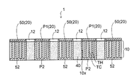
まず、図5を参照しながら、実施形態の配線基板1の基本構造について説明する。図5に示すように、実施形態の配線基板1では、酸化アルミニウム基板10の一方の面に第1接続パッドP1が配置されている。
First, the basic structure of the
また、酸化アルミニウム基板10の他方の面に第1接続パッドP1に対応して第2接続パッドP2が配置されている。第1接続パッドP1及び第2接続パッドP2は、酸化アルミニウム基板10に形成された複数の貫通導体TCによって相互接続されている。
A second connection pad P2 is arranged on the other surface of the
また、酸化アルミニウム基板10の一方に面に第1接続パッドP1を取り囲むように第1金属層50が配置されている。さらに、酸化アルミニウム基板10の他方の面に、第1金属層50に対応して、第2接続パッドP2を取り囲むように第2金属層52が配置されている。
A
両面側の第1金属層50及び第2金属層52は、酸化アルミニウム基板10に形成された複数の貫通導体TCによって相互接続されている。
The
第1接続パッドP1と第1金属層50との間の環状部分の酸化アルミニウム基板10に、厚み方向に貫通する弾性体40が一体的に形成されている。また、第1接続パッドP1と第1金属層50との間の環状領域の酸化アルミニウム基板10の上に永久レジスト層12が配置されている。
An
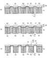
次に、図6(a)及び(b)を参照して、図5の第1、第2金属層50,52が分離されて、電源プレーン及びグランドプレーンが形成された形態を説明しながらさらに詳しく説明する。本実施形態では、電源パターン及びグランドパターンとして、電源プレーン及びグランドプレーンを例示する。 Next, with reference to FIGS. 6A and 6B, the first and second metal layers 50 and 52 of FIG. 5 are separated to further explain a form in which a power plane and a ground plane are formed. explain in detail. In this embodiment, a power plane and a ground plane are exemplified as the power pattern and the ground pattern.
図6(a)は実施形態の配線基板の断面を斜視的にみた断面斜視図であり、図6(b)は図6(a)のII−IIに沿った断面図に相当する。 6A is a cross-sectional perspective view of the cross-section of the wiring board of the embodiment, and FIG. 6B corresponds to a cross-sectional view taken along line II-II in FIG.
図6(a)及び(b)に示すように、実施形態の配線基板1では、酸化アルミニウム基板10の一方の面に複数の円形の第1接続パッドP1が相互に分離された状態で配置されている。酸化アルミニウム基板10は絶縁基板の一例である。
As shown in FIGS. 6A and 6B, in the
そして、第1接続パッドP1を同心円状に取り囲むようにして第1電源プレーン50aが配置されている。また同様に、第1接続パッドP1を同心円状に取り囲むようにして第1グランドプレーン50bが配置されている。
A
第1電源プレーン50a及び第1グランドプレーン50bは、酸化アルミニウム基板10上の中央部で分離され、電気的に絶縁されている。さらに、第1接続パッドP1と第1金属層50との間の環状領域の酸化アルミニウム基板10の上に永久レジスト層12が配置されている。永久レジスト層12は絶縁層の一例である。
The
また、第1電源プレーン50a及び第1グランドプレーン50bの各々は、酸化アルミニウム基板10上の第1接続パッドP1及び永久レジスト層12を除く領域にそれぞれプレーン層として一体的に形成されている。
Further, each of the
図6(b)に注目すると、第1接続パッドP1に対応する部分の酸化アルミニウム基板10に複数の貫通導体TCが配置されている。第1接続パッドP1とその下の複数の貫通導体TCとが電気的に接続されている。
When attention is paid to FIG. 6B, a plurality of through conductors TC are arranged on the
また、酸化アルミニウム基板10の他方の面において、第1接続パッドP1に対応する部分に、複数の貫通導体TCに繋がる第2接続パッドP2が形成されている。これにより、第1接続パッドP1は複数の貫通導体TCを介して第2接続パッドP2に電気的に接続されている。
In addition, on the other surface of the
また、第1電源プレーン50a及び第1グランドプレーン50bに対応する部分の酸化アルミニウム基板10に複数の貫通導体TCがそれぞれ配置されている。酸化アルミニウム基板10の他方の面において、第1電源プレーン50aに対応する部分に、複数の貫通導体TCに繋がる第2電源プレーン52aが形成されている。これにより、第1電源プレーン50aは複数の貫通導体TCを介して第2電源プレーン52aに電気的に接続されている。
In addition, a plurality of through conductors TC are respectively disposed on portions of the
また同様に、酸化アルミニウム基板10の他方の面において、第1グランドプレーン50bに対応する部分に、複数の貫通導体TCに繋がる第2グランドプレーン52bが形成されている。これにより、第1グランドプレーン50bは複数の貫通導体TCを介して第2グランドプレーン52bに電気的に接続されている。
Similarly, on the other surface of the
本実施形態では、第1接続パッドP1を取り囲む第1金属層50を2つに分離して第1電源プレーン50a及び第1グランドプレーン50bとしているが、分割数は任意の数(2以上)に設定することができる。また、第2接続パッドP2を取り囲む第2金属層52においても、第1金属層50の分割に合わせて任意の数に分割される。
In the present embodiment, the
前述した製造方法のように、第1接続パッドP1となるシード金属層20の下の酸化アルミニウム基板10の複数のスルーホールTHに、電解めっきにより、貫通導体TCが充填され、続いてそれらに繋がる第2接続パッドP2が形成される。
As in the manufacturing method described above, the through conductors TC are filled in the plurality of through holes TH of the
これにより、第2接続パッドP2は、第1接続パッドP1に対応する領域に自己整合的に配置される。従って、接続パッドが狭ピッチ化される場合であっても、第1接続パッドP1と第2接続パッドP2とが位置ずれして他の電気系統の貫通導体TCと短絡するおそれがない。 Thus, the second connection pad P2 is arranged in a self-aligned manner in a region corresponding to the first connection pad P1. Therefore, even when the connection pads are narrowed, there is no possibility that the first connection pads P1 and the second connection pads P2 are misaligned and short-circuited with the through conductors TC of other electrical systems.
また、第1接続パッドP1の周囲の永久レジスト層12に対応する部分の酸化アルミニウム基板10には、その厚み方向に貫通するように弾性体40が一体的に充填されている。
In addition, the
このように、本実施形態の配線基板1では、第1、第2接続パッドP1,P2に複数の貫通導体TCを接続した垂直接続配線の周囲に、絶縁性の弾性体40を一体的に配置した同軸構造を採用している。
As described above, in the
さらに、第1接続パッドP1を取り囲むように第1グランドプレーン50bを容易に配置することができる。このため、接続パッドが狭ピッチ化される場合であっても、高周波回路でのクロストークを低減することができる。
Furthermore, the
また、電源−グランド間の共振による放射ノイズを抑制するためには、電源プレーン50a,52aとグランドプレーン50b,52bとの間に比較的大きな容量のキャパシタが配置されることが好ましい。
Further, in order to suppress radiation noise due to resonance between the power supply and the ground, it is preferable that a capacitor having a relatively large capacitance is disposed between the
このような観点から、図6(a)及び(b)では、電源プレーン50a,52aとグランドプレーン50b,52bとの間の領域Aの酸化アルミニウム基板10にも複数の貫通導体TCが配置されている。この領域Aの酸化アルミニウム基板10に配置される複数の貫通導体TCは電気的に孤立しており、他の導体に接続されていない。
From this point of view, in FIGS. 6A and 6B, a plurality of through conductors TC are also arranged on the
これにより、電源プレーン50a,52aと、貫通導体TCの間に配置された酸化アルミニウム基板10と、グランドプレーン50b,52bとによりキャパシタが形成される。
Thereby, a capacitor is formed by the
このようにして形成されるキャパシタは、電源プレーン50a,52aとグランドプレーン50b,52bとの間の領域Aの酸化アルミニウム基板10に絶縁性の弾性体40を一体的に充填する場合よりも大きな容量が得られる。このため、放射ノイズの抑制効果を高めることができる。
The capacitor thus formed has a larger capacity than the case where the insulating
ここで、図7〜図8を参照しながら、電源プレーン50a,52aとグランドプレーン50b,52bとを分離させ、かつそれらの間の領域Aの酸化アルミニウム基板10に複数の貫通導体TCを配置する製造方法について説明する。
Here, referring to FIGS. 7 to 8, the
図7(a)に示すように、前述した図1(a)〜図2(c)と同様な方法により、多数のスルーホールTHが設けられた酸化アルミニウム基板10を作成し、環状の永久レジスト層12を形成した後に、下地金属層22を形成する。
As shown in FIG. 7A, an
次いで、図7(b)に示すように、第1電源プレーン50aと第1グランドプレーン50bとを分離する部分の下地金属層22の上に、フォトレジスト層15をディスペンサなどにより直線状のパターンで形成する。さらに、図7(c)に示すように、前述した図2(d)と同様な方法により、下地金属層22及びフォトレジスト層15の上に金属めっき層24を形成してシード金属層20を得る。
Next, as shown in FIG. 7B, a
続いて、図7(d)に示すように、前述した図3(a)及び(b)と同様な方法により、シード金属層20が配置された部分の酸化アルミニウム基板10のスルーホールTHに貫通導体TCを充填する。さらに連続して、複数の貫通導体TCに繋がる第2接続パッドP2及び第2金属層52を形成する。
Subsequently, as shown in FIG. 7 (d), through the through hole TH of the
次いで、図8(a)に示すように、前述した図3(c)と同様な方法により、永久レジスト層12が配置された部分の酸化アルミニウム基板10を除去して開口部10xを形成する。
Next, as shown in FIG. 8A, the
その後に、図8(b)に示すように、前述した図4(a)と同様な方法により、酸化アルミニウム基板10の開口部10xに弾性体40を充填する。
After that, as shown in FIG. 8B, the
次いで、図8(c)に示すように、前述した図4(c)及び図5と同様に、シード金属層20を厚みの途中まで除去することにより、永久レジスト層12及びフォトレジスト層15の各上面を露出させる。これにより、永久レジスト層12及びフォトレジスト層15の横方向の凹領域に第1接続パッドP1及び第1金属層50を得る。
Next, as shown in FIG. 8C, the
さらに、図8(d)に示すように、フォトレジスト層15をストリッパーで除去した後、その底部の下地金属層22をウェットエッチングにより除去する。このとき、永久レジスト層12は完全に硬化しているため、ストリッパーでは除去されずに残される。
Further, as shown in FIG. 8D, after removing the
これにより、酸化アルミニウム基板10の上面において、第1電源プレーン50aと第1グランドプレーン50bとが分離されて配置される。
Thereby, on the upper surface of the
その後に、酸化アルミニウム基板10の下面において、第2金属層52の分離する部分をフォトリソグラフィ及びウェットエッチングにより除去する。これにより、酸化アルミニウム基板10の下面においても、第2電源プレーン52aと第2グランドプレーン52bとが分離されて配置される。
Thereafter, the portion where the
なお、シード金属層20の厚みが比較的薄い場合は、前述した図7(b)でフォトレジスト層15を形成せずに分離部分にもシード金属層20を形成し、シード金属層20の分離する部分をフォトリソグラフィ及びエッチングによって除去してもよい。
When the thickness of the
また、酸化アルミニウム基板10の下面の第2金属層52を分離する他の方法として、以下の方法を採用してもよい。まず、前述した図7(d)の貫通導体TCを充填する工程で、酸化アルミニウム基板10のスルーホールTHの下側開口端まで貫通導体TCを埋め込んだ後に電解めっきを一旦中止する。次いで、酸化アルミニウム基板10の下面の分離部分に直線状パターンのフォトレジスト層をディスペンサなどで形成する。
Further, as another method for separating the
そして、再び、酸化アルミニウム基板10に電解めっきを施して貫通導体TCに繋がる第2接続パッドP2及び第2金属層52を形成する。その後に、フォトレジスト層が除去される。これにより、第2金属層52は、フォトレジスト層によって第2電源プレーン52aと第2グランドプレーン52bとに分離された状態で形成される。
Then, again, the
以上の方法により、電源プレーン50a,52aとグランドプレーン50b,52bとを分離させ、かつそれらの間の領域の酸化アルミニウム基板10に複数の貫通導体TCが配置された構造を製造することができる。
By the above method, it is possible to manufacture a structure in which the
あるいは、図9に示す変形例の配線基板1aのように、電源−グランド間の共振による放射ノイズが問題にならない場合は、電源プレーン50a,52aとグランドプレーン50b,52bとの間の領域の酸化アルミニウム基板10に一括して弾性体40が充填されるようにしてもよい。
Alternatively, when radiation noise due to resonance between the power supply and the ground does not become a problem as in the
この場合は、前述した図7(a)の工程において、下地金属層22を形成する前に、第1電源プレーン50aと第1グランドプレーン50bとを分離する部分にも永久レジスト層12を形成すればよい。
In this case, in the step of FIG. 7A described above, the permanent resist
図10には、実施形態の配線基板の上に半導体チップがフリップチップ接続された半導体装置の一例が示されている。 FIG. 10 shows an example of a semiconductor device in which a semiconductor chip is flip-chip connected to the wiring board of the embodiment.
図10に示すように、半導体チップ60の電極を前述した図8(d)の配線基板1の第1接続パッドP1、第1電源プレーン50a及び第1グランドプレーン50bの各接続部の上にはんだを介して配置する。
As shown in FIG. 10, the electrodes of the
さらに、250℃程度の温度でリフロー加熱することにより、半導体チップ60をバンプ電極62を介して配線基板1にフリップチップ接続する。配線基板1の第1接続パッドP1などの表面に無電解めっきで形成された錫層が設けられていてもよい。
Further, the
このとき、リフロー加熱する際に、酸化アルミニウム基板10と半導体チップ60との間の熱膨張係数の差によって熱応力が発生する。しかし、本実施形態の配線基板1では、第1接続パッドP1の周りの部分の酸化アルミニウム基板10に、その厚み方向に貫通する弾性体40が一体的に形成されている。
At this time, when reflow heating is performed, thermal stress is generated due to a difference in thermal expansion coefficient between the
このため、配線基板1内で上下方向又は水平方向にずれるような応力が発生しても、その応力を吸収して緩和することができる。
For this reason, even if a stress that shifts in the vertical direction or the horizontal direction is generated in the
これにより、半導体チップ60を信頼性よく配線基板1にフリップチップ接続することができると共に、半導体装置の長期的な信頼性を確保することができる。
Thereby, the
さらに、配線基板1の下面側の第2接続パッドP2と、第2電源プレーン52a及び第2グランドプレーン52bの各接続部とにはんだボールを搭載するなどして外部接続端子64を設ける。
Further,
本実施形態の配線基板1では、基板内部に充填された弾性体40の作用によって応力を緩和するため、弾性体40はフリーな状態で配置されることが望ましい。このような観点から、半導体チップ60の下側に充填されるアンダーフィル樹脂は弾性体40を固定するように機能するため、アンダーフィル樹脂を省略する構造とする方がよい。
In the
弾性体40がアンダーフィル樹脂で固定されても問題にならない場合は、アンダーフィル樹脂を形成しても差し使えない。
If there is no problem even if the
実装する電子部品として半導体チップ60を例示したが、各種の電子部品の実装基板として使用することができる。また、本実施形態の配線基板は、実装基板と電子部品との間に配置されるインターポーザとして使用してもよい。
Although the
1,1a…配線基板、10…酸化アルミニウム基板、10a…アルミニウム基板、10b…アルミニウム部、10x…開口部、12…永久レジスト層、15…フォトレジスト層、20…シード金属層、22…下地金属層、24…金属めっき層、40…弾性体、40a…樹脂フィルム、42…押圧部材、50…第1金属層、50a…第1電源プレーン、50b…第1グランドプレーン、52…第2金属層、52a…第2電源プレーン、52b…第2グランドプレーン、60…半導体チップ、62…バンプ電極、64…外部接続端子、H…ホール、P1…第1接続パッド、P2…第2接続パッド、TC…貫通導体、TH…スルーホール。
DESCRIPTION OF
Claims (10)
前記酸化アルミニウム基板の一方の面に配置された第1接続パッドと、
前記酸化アルミニウム基板の他方の面に、前記第1接続パッドに対応して配置された第2接続パッドと、
前記第1接続パッドを取り囲んで配置された第1金属層と、
前記第1金属層に対応して配置され、前記第2接続パッドを取り囲む第2金属層と、
前記第1接続パッドと前記第2接続パッドとを接続すると共に、前記第1金属層と前記第2金属層とを接続する前記複数の貫通導体と、
前記第1接続パッドと前記第1金属層との間の部分の前記酸化アルミニウム基板の上に配置された絶縁層と、
平面視で前記絶縁層と重なる領域の前記酸化アルミニウム基板の部分に貫通して形成された開口部と、
前記酸化アルミニウム基板の開口部に充填された弾性体と
を有し、
前記第1接続パッド、前記第2接続パッド、前記第1金属層、及び前記第2金属層に、前記複数の貫通導体がそれぞれ接続されていることを特徴とする配線基板。 An aluminum oxide substrate provided with a plurality of through conductors penetrating in the thickness direction;
A first connection pad disposed on one surface of the aluminum oxide substrate ;
A second connection pad disposed on the other surface of the aluminum oxide substrate corresponding to the first connection pad;
A first metal layer disposed surrounding the first connection pad;
A second metal layer disposed corresponding to the first metal layer and surrounding the second connection pad;
The plurality of through conductors for connecting the first connection pad and the second connection pad and for connecting the first metal layer and the second metal layer,
An insulating layer disposed on the aluminum oxide substrate in a portion between the first connection pad and the first metal layer;
An opening formed through a portion of the aluminum oxide substrate in a region overlapping the insulating layer in plan view;
An elastic body filled in the opening of the aluminum oxide substrate ,
The wiring board, wherein the plurality of through conductors are connected to the first connection pad, the second connection pad, the first metal layer, and the second metal layer, respectively.
前記第1金属層及び前記第2金属層の分離された部分の前記酸化アルミニウム基板に、電気的に孤立した前記複数の貫通導体が配置されていることを特徴とする請求項2に記載の配線基板。 In each of the first metal layer and the second metal layer, the divided adjacent metal layers are a power pattern and a ground pattern,
3. The wiring according to claim 2, wherein the plurality of electrically isolated through conductors are arranged on the aluminum oxide substrate in a separated portion of the first metal layer and the second metal layer. substrate.
前記酸化アルミニウム基板の上に環状パターンの絶縁層を形成する工程と、
前記酸化アルミニウム基板及び前記絶縁層の上にシード金属層を形成する工程と、
前記シード金属層を給電経路とする電解めっきにより、前記酸化アルミニウム基板のスルーホールに貫通導体を充填する工程と、
前記絶縁層の下の前記酸化アルミニウム基板を除去して開口部を形成する工程と、
前記酸化アルミニウム基板の開口部に弾性体を充填する工程とを有することを特徴とする配線基板の製造方法。 Preparing an aluminum oxide substrate having a plurality of through holes;
Forming an insulating layer of an annular pattern on the aluminum oxide substrate ;
Forming a seed metal layer on the aluminum oxide substrate and the insulating layer;
Filling the through hole of the aluminum oxide substrate with a through conductor by electrolytic plating using the seed metal layer as a power feeding path;
Removing the aluminum oxide substrate under the insulating layer to form an opening;
And a step of filling an elastic body in the opening of the aluminum oxide substrate .
前記絶縁層が露出するまで前記シード金属層を除去して、前記環状パターンの絶縁層の内側に第1接続パッドを形成すると共に、前記絶縁層の外側に第1金属層を形成する工程を有することを特徴とする請求項6に記載の配線基板の製造方法。 After the step of filling the elastic body,
Removing the seed metal layer until the insulating layer is exposed, forming a first connection pad inside the insulating layer of the annular pattern, and forming a first metal layer outside the insulating layer; The method for manufacturing a wiring board according to claim 6.
前記第1接続パッドに対応する部分の前記酸化アルミニウム基板の下面に、前記貫通導体に繋がる第2接続パッドを形成すると共に、前記第1金属層に対応する部分の前記酸化アルミニウム基板の下面に、前記貫通導体に繋がる第2金属層を形成することを含むことを特徴とする請求項7に配線基板の製造方法。 The step of filling the through conductors includes
The lower surface of the aluminum oxide substrate in a portion corresponding to the first connection pad, thereby forming a second connection pad connected to the through conductors, the lower surface of the aluminum oxide substrate in a portion corresponding to the first metal layer, The method for manufacturing a wiring board according to claim 7, further comprising forming a second metal layer connected to the through conductor.
Priority Applications (2)
| Application Number | Priority Date | Filing Date | Title |
|---|---|---|---|
| JP2013051537A JP6082284B2 (en) | 2013-03-14 | 2013-03-14 | Wiring board and manufacturing method thereof |
| US14/202,220 US9204544B2 (en) | 2013-03-14 | 2014-03-10 | Wiring substrate and method of manufacturing the same |
Applications Claiming Priority (1)
| Application Number | Priority Date | Filing Date | Title |
|---|---|---|---|
| JP2013051537A JP6082284B2 (en) | 2013-03-14 | 2013-03-14 | Wiring board and manufacturing method thereof |
Publications (3)
| Publication Number | Publication Date |
|---|---|
| JP2014179411A JP2014179411A (en) | 2014-09-25 |
| JP2014179411A5 JP2014179411A5 (en) | 2016-01-21 |
| JP6082284B2 true JP6082284B2 (en) | 2017-02-15 |
Family
ID=51522422
Family Applications (1)
| Application Number | Title | Priority Date | Filing Date |
|---|---|---|---|
| JP2013051537A Active JP6082284B2 (en) | 2013-03-14 | 2013-03-14 | Wiring board and manufacturing method thereof |
Country Status (2)
| Country | Link |
|---|---|
| US (1) | US9204544B2 (en) |
| JP (1) | JP6082284B2 (en) |
Family Cites Families (12)
| Publication number | Priority date | Publication date | Assignee | Title |
|---|---|---|---|---|
| US4942400A (en) * | 1990-02-09 | 1990-07-17 | General Electric Company | Analog to digital converter with multilayer printed circuit mounting |
| JP3014503B2 (en) * | 1991-08-05 | 2000-02-28 | 日本特殊陶業株式会社 | Package for integrated circuit |
| JP2002289998A (en) * | 2001-03-23 | 2002-10-04 | Citizen Watch Co Ltd | Circuit board and manufacturing method thereof |
| US6828513B2 (en) * | 2002-04-30 | 2004-12-07 | Texas Instruments Incorporated | Electrical connector pad assembly for printed circuit board |
| JP2004273480A (en) * | 2003-03-05 | 2004-09-30 | Sony Corp | Wiring board, its manufacturing method, and semiconductor device |
| US7583513B2 (en) * | 2003-09-23 | 2009-09-01 | Intel Corporation | Apparatus for providing an integrated printed circuit board registration coupon |
| JP4654942B2 (en) * | 2006-02-28 | 2011-03-23 | ミネベア株式会社 | Surface lighting device |
| JP5344667B2 (en) | 2007-12-18 | 2013-11-20 | 太陽誘電株式会社 | Circuit board, manufacturing method thereof, and circuit module |
| JP5385682B2 (en) * | 2009-05-19 | 2014-01-08 | 新光電気工業株式会社 | Electronic component mounting structure |
| JP2011014612A (en) * | 2009-06-30 | 2011-01-20 | Ibiden Co Ltd | Wiring board and method for manufacturing wiring board |
| JP2011151185A (en) * | 2010-01-21 | 2011-08-04 | Shinko Electric Ind Co Ltd | Wiring board and semiconductor device |
| US8870579B1 (en) * | 2011-01-14 | 2014-10-28 | Paricon Technologies Corporation | Thermally and electrically enhanced elastomeric conductive materials |
-
2013
- 2013-03-14 JP JP2013051537A patent/JP6082284B2/en active Active
-
2014
- 2014-03-10 US US14/202,220 patent/US9204544B2/en active Active
Also Published As
| Publication number | Publication date |
|---|---|
| JP2014179411A (en) | 2014-09-25 |
| US9204544B2 (en) | 2015-12-01 |
| US20140262465A1 (en) | 2014-09-18 |
Similar Documents
| Publication | Publication Date | Title |
|---|---|---|
| US8324513B2 (en) | Wiring substrate and semiconductor apparatus including the wiring substrate | |
| TWI504318B (en) | Printed circuit board and method of manufacturing the same | |
| US9693458B2 (en) | Printed wiring board, method for manufacturing printed wiring board and package-on-package | |
| US9307643B2 (en) | Substrate with built-in electronic component and method for manufacturing substrate with built-in electronic component | |
| JP6210777B2 (en) | Bump structure, wiring board, semiconductor device, and bump structure manufacturing method | |
| KR20060061227A (en) | Method of manufacturing a circuit substrate and method of manufacturing a structure for mounting electronic parts | |
| TW201601262A (en) | Interposer, semiconductor device, interposer manufacturing method, and semiconductor device manufacturing method | |
| JP2010021516A (en) | Manufacturing method of electronic-element-incorporated printed circuit board | |
| KR101835782B1 (en) | Thin film capacitor manufacturing method, integrated circuit mounting substrate, and semiconductor device provided with integrated circuit mounting substrate | |
| CN105704926B (en) | Method for producing electronic module and electronic module | |
| JP2013004576A (en) | Semiconductor device | |
| JP6282425B2 (en) | Wiring board manufacturing method | |
| JP2007081100A (en) | Wiring substrate, and manufacturing method thereof | |
| JP2015198094A (en) | Interposer, semiconductor device, and method of manufacturing them | |
| JP4227973B2 (en) | Substrate, electronic component, and manufacturing method thereof | |
| WO2016114133A1 (en) | Interposer, semiconductor device, and method for manufacture thereof | |
| JP2017005081A (en) | Interposer, semiconductor device, and method of manufacturing them | |
| JP6082284B2 (en) | Wiring board and manufacturing method thereof | |
| KR102141102B1 (en) | Method for manufacturing semiconductor package substrate and semiconductor package substrate manufactured using the same | |
| JP5980554B2 (en) | Electrical connection member, inspection method, and manufacturing method of electrical connection member | |
| US20150027977A1 (en) | Method of manufacturing wiring board | |
| JP6533089B2 (en) | Wiring board | |
| JP5154963B2 (en) | Wiring board manufacturing method | |
| JP5680589B2 (en) | Wiring board | |
| JP2010278032A (en) | Surface mounted capacitor |
Legal Events
| Date | Code | Title | Description |
|---|---|---|---|
| A521 | Written amendment |
Free format text: JAPANESE INTERMEDIATE CODE: A523 Effective date: 20151125 |
|
| A621 | Written request for application examination |
Free format text: JAPANESE INTERMEDIATE CODE: A621 Effective date: 20151125 |
|
| A977 | Report on retrieval |
Free format text: JAPANESE INTERMEDIATE CODE: A971007 Effective date: 20160929 |
|
| A131 | Notification of reasons for refusal |
Free format text: JAPANESE INTERMEDIATE CODE: A131 Effective date: 20161011 |
|
| A521 | Written amendment |
Free format text: JAPANESE INTERMEDIATE CODE: A523 Effective date: 20161109 |
|
| TRDD | Decision of grant or rejection written | ||
| A01 | Written decision to grant a patent or to grant a registration (utility model) |
Free format text: JAPANESE INTERMEDIATE CODE: A01 Effective date: 20170110 |
|
| A61 | First payment of annual fees (during grant procedure) |
Free format text: JAPANESE INTERMEDIATE CODE: A61 Effective date: 20170120 |
|
| R150 | Certificate of patent or registration of utility model |
Ref document number: 6082284 Country of ref document: JP Free format text: JAPANESE INTERMEDIATE CODE: R150 |