JP6080343B2 - Image sensor and manufacturing method thereof - Google Patents
Image sensor and manufacturing method thereof Download PDFInfo
- Publication number
- JP6080343B2 JP6080343B2 JP2011166382A JP2011166382A JP6080343B2 JP 6080343 B2 JP6080343 B2 JP 6080343B2 JP 2011166382 A JP2011166382 A JP 2011166382A JP 2011166382 A JP2011166382 A JP 2011166382A JP 6080343 B2 JP6080343 B2 JP 6080343B2
- Authority
- JP
- Japan
- Prior art keywords
- color filter
- unit
- pixel
- color
- photodiode
- Prior art date
- Legal status (The legal status is an assumption and is not a legal conclusion. Google has not performed a legal analysis and makes no representation as to the accuracy of the status listed.)
- Active
Links
- 238000004519 manufacturing process Methods 0.000 title description 26
- 238000002834 transmittance Methods 0.000 claims description 41
- 230000003595 spectral effect Effects 0.000 claims description 31
- 238000003384 imaging method Methods 0.000 claims description 20
- 239000003086 colorant Substances 0.000 claims description 16
- 238000005516 engineering process Methods 0.000 description 34
- 238000012545 processing Methods 0.000 description 24
- 239000000203 mixture Substances 0.000 description 21
- 238000012937 correction Methods 0.000 description 16
- 210000001747 pupil Anatomy 0.000 description 15
- 238000010586 diagram Methods 0.000 description 13
- 238000000034 method Methods 0.000 description 13
- 238000010030 laminating Methods 0.000 description 11
- 238000005286 illumination Methods 0.000 description 9
- 239000004065 semiconductor Substances 0.000 description 7
- 239000002184 metal Substances 0.000 description 6
- 239000000758 substrate Substances 0.000 description 6
- 238000001459 lithography Methods 0.000 description 4
- 230000008569 process Effects 0.000 description 4
- 230000035945 sensitivity Effects 0.000 description 4
- 239000000463 material Substances 0.000 description 3
- 230000009467 reduction Effects 0.000 description 3
- 230000015572 biosynthetic process Effects 0.000 description 2
- 238000006243 chemical reaction Methods 0.000 description 2
- 210000000887 face Anatomy 0.000 description 2
- 230000004048 modification Effects 0.000 description 2
- 238000012986 modification Methods 0.000 description 2
- 238000003491 array Methods 0.000 description 1
- 230000005540 biological transmission Effects 0.000 description 1
- 230000015556 catabolic process Effects 0.000 description 1
- 230000008859 change Effects 0.000 description 1
- 239000011248 coating agent Substances 0.000 description 1
- 238000000576 coating method Methods 0.000 description 1
- 230000000295 complement effect Effects 0.000 description 1
- 238000007796 conventional method Methods 0.000 description 1
- 238000006731 degradation reaction Methods 0.000 description 1
- 239000004973 liquid crystal related substance Substances 0.000 description 1
- 239000011159 matrix material Substances 0.000 description 1
- 229910044991 metal oxide Inorganic materials 0.000 description 1
- 150000004706 metal oxides Chemical class 0.000 description 1
- 230000003287 optical effect Effects 0.000 description 1
- 230000035699 permeability Effects 0.000 description 1
- 239000000049 pigment Substances 0.000 description 1
- 238000004904 shortening Methods 0.000 description 1
- 238000001228 spectrum Methods 0.000 description 1
- 230000007480 spreading Effects 0.000 description 1
- 238000003892 spreading Methods 0.000 description 1
Images


Classifications
-
- H—ELECTRICITY
- H04—ELECTRIC COMMUNICATION TECHNIQUE
- H04N—PICTORIAL COMMUNICATION, e.g. TELEVISION
- H04N23/00—Cameras or camera modules comprising electronic image sensors; Control thereof
- H04N23/10—Cameras or camera modules comprising electronic image sensors; Control thereof for generating image signals from different wavelengths
- H04N23/12—Cameras or camera modules comprising electronic image sensors; Control thereof for generating image signals from different wavelengths with one sensor only
-
- H—ELECTRICITY
- H01—ELECTRIC ELEMENTS
- H01L—SEMICONDUCTOR DEVICES NOT COVERED BY CLASS H10
- H01L27/00—Devices consisting of a plurality of semiconductor or other solid-state components formed in or on a common substrate
- H01L27/14—Devices consisting of a plurality of semiconductor or other solid-state components formed in or on a common substrate including semiconductor components sensitive to infrared radiation, light, electromagnetic radiation of shorter wavelength or corpuscular radiation and specially adapted either for the conversion of the energy of such radiation into electrical energy or for the control of electrical energy by such radiation
- H01L27/144—Devices controlled by radiation
- H01L27/146—Imager structures
- H01L27/14601—Structural or functional details thereof
- H01L27/14603—Special geometry or disposition of pixel-elements, address-lines or gate-electrodes
- H01L27/14605—Structural or functional details relating to the position of the pixel elements, e.g. smaller pixel elements in the center of the imager compared to pixel elements at the periphery
-
- H—ELECTRICITY
- H01—ELECTRIC ELEMENTS
- H01L—SEMICONDUCTOR DEVICES NOT COVERED BY CLASS H10
- H01L27/00—Devices consisting of a plurality of semiconductor or other solid-state components formed in or on a common substrate
- H01L27/14—Devices consisting of a plurality of semiconductor or other solid-state components formed in or on a common substrate including semiconductor components sensitive to infrared radiation, light, electromagnetic radiation of shorter wavelength or corpuscular radiation and specially adapted either for the conversion of the energy of such radiation into electrical energy or for the control of electrical energy by such radiation
- H01L27/144—Devices controlled by radiation
- H01L27/146—Imager structures
- H01L27/14601—Structural or functional details thereof
- H01L27/1462—Coatings
- H01L27/14621—Colour filter arrangements
-
- H—ELECTRICITY
- H01—ELECTRIC ELEMENTS
- H01L—SEMICONDUCTOR DEVICES NOT COVERED BY CLASS H10
- H01L27/00—Devices consisting of a plurality of semiconductor or other solid-state components formed in or on a common substrate
- H01L27/14—Devices consisting of a plurality of semiconductor or other solid-state components formed in or on a common substrate including semiconductor components sensitive to infrared radiation, light, electromagnetic radiation of shorter wavelength or corpuscular radiation and specially adapted either for the conversion of the energy of such radiation into electrical energy or for the control of electrical energy by such radiation
- H01L27/144—Devices controlled by radiation
- H01L27/146—Imager structures
- H01L27/14601—Structural or functional details thereof
- H01L27/14625—Optical elements or arrangements associated with the device
-
- H—ELECTRICITY
- H01—ELECTRIC ELEMENTS
- H01L—SEMICONDUCTOR DEVICES NOT COVERED BY CLASS H10
- H01L27/00—Devices consisting of a plurality of semiconductor or other solid-state components formed in or on a common substrate
- H01L27/14—Devices consisting of a plurality of semiconductor or other solid-state components formed in or on a common substrate including semiconductor components sensitive to infrared radiation, light, electromagnetic radiation of shorter wavelength or corpuscular radiation and specially adapted either for the conversion of the energy of such radiation into electrical energy or for the control of electrical energy by such radiation
- H01L27/144—Devices controlled by radiation
- H01L27/146—Imager structures
- H01L27/14643—Photodiode arrays; MOS imagers
-
- H—ELECTRICITY
- H01—ELECTRIC ELEMENTS
- H01L—SEMICONDUCTOR DEVICES NOT COVERED BY CLASS H10
- H01L27/00—Devices consisting of a plurality of semiconductor or other solid-state components formed in or on a common substrate
- H01L27/14—Devices consisting of a plurality of semiconductor or other solid-state components formed in or on a common substrate including semiconductor components sensitive to infrared radiation, light, electromagnetic radiation of shorter wavelength or corpuscular radiation and specially adapted either for the conversion of the energy of such radiation into electrical energy or for the control of electrical energy by such radiation
- H01L27/144—Devices controlled by radiation
- H01L27/146—Imager structures
- H01L27/14683—Processes or apparatus peculiar to the manufacture or treatment of these devices or parts thereof
-
- H—ELECTRICITY
- H04—ELECTRIC COMMUNICATION TECHNIQUE
- H04N—PICTORIAL COMMUNICATION, e.g. TELEVISION
- H04N23/00—Cameras or camera modules comprising electronic image sensors; Control thereof
- H04N23/10—Cameras or camera modules comprising electronic image sensors; Control thereof for generating image signals from different wavelengths
- H04N23/13—Cameras or camera modules comprising electronic image sensors; Control thereof for generating image signals from different wavelengths with multiple sensors
-
- H—ELECTRICITY
- H04—ELECTRIC COMMUNICATION TECHNIQUE
- H04N—PICTORIAL COMMUNICATION, e.g. TELEVISION
- H04N25/00—Circuitry of solid-state image sensors [SSIS]; Control thereof
- H04N25/70—SSIS architectures; Circuits associated therewith
- H04N25/76—Addressed sensors, e.g. MOS or CMOS sensors
-
- H—ELECTRICITY
- H04—ELECTRIC COMMUNICATION TECHNIQUE
- H04N—PICTORIAL COMMUNICATION, e.g. TELEVISION
- H04N2209/00—Details of colour television systems
- H04N2209/04—Picture signal generators
- H04N2209/041—Picture signal generators using solid-state devices
- H04N2209/048—Picture signal generators using solid-state devices having several pick-up sensors
- H04N2209/049—Picture signal generators using solid-state devices having several pick-up sensors having three pick-up sensors
-
- Y—GENERAL TAGGING OF NEW TECHNOLOGICAL DEVELOPMENTS; GENERAL TAGGING OF CROSS-SECTIONAL TECHNOLOGIES SPANNING OVER SEVERAL SECTIONS OF THE IPC; TECHNICAL SUBJECTS COVERED BY FORMER USPC CROSS-REFERENCE ART COLLECTIONS [XRACs] AND DIGESTS
- Y10—TECHNICAL SUBJECTS COVERED BY FORMER USPC
- Y10T—TECHNICAL SUBJECTS COVERED BY FORMER US CLASSIFICATION
- Y10T29/00—Metal working
- Y10T29/49—Method of mechanical manufacture
- Y10T29/49826—Assembling or joining
Description
本技術は、撮像素子およびその製造方法に関し、特に、オンチップレンズとフォトダイオードとの間で発生する混色を低減できる、撮像素子およびその製造方法に関する。 The present technology relates to an imaging device and a manufacturing method thereof, and more particularly, to an imaging device and a manufacturing method thereof that can reduce color mixture that occurs between an on-chip lens and a photodiode.
従来から、CMOS(Complementary Metal Oxide Semiconductor)イメージセンサ等の撮像素子には、一般的に、1種類のカラーフィルタが1層のみ配置される構成の画素が採用されている(例えば、特許文献1参照)。その他、例えば、2種類のカラーフィルタが積層されて配置される構成の画素(例えば、特許文献2参照)や、配置されるカラーフィルタの高さが色別に異なる構成の画素(例えば、特許文献3参照)が、従来の撮像素子に採用される場合がある。 2. Description of the Related Art Conventionally, pixels having a configuration in which only one layer of one type of color filter is arranged have been adopted for imaging devices such as CMOS (Complementary Metal Oxide Semiconductor) image sensors (see, for example, Patent Document 1). ). In addition, for example, a pixel having a configuration in which two kinds of color filters are stacked (see, for example, Patent Document 2), or a pixel having a configuration in which the height of the arranged color filter is different for each color (for example, Patent Document 3). May be employed in a conventional image sensor.
しかしながら、特許文献1乃至3を含む従来の構成の画素では、オンチップレンズにより集光されてカラーフィルタを透過した光が、フォトダイオードに入射するまでの間に隣接画素のフォトダイオードに漏れ込むことによって、混色が発生する。混色は、S/N(Signal to Noise Ratio)や色再現性の低下につながるおそれがある。このため、オンチップレンズとフォトダイオードとの間で発生する混色を低減する手法が要求されている状況である。
However, in the pixels having the conventional configuration including
本技術は、このような状況に鑑みてなされたものであり、オンチップレンズとフォトダイオードとの間で発生する混色を低減できるようにしたものである。 The present technology has been made in view of such a situation, and is capable of reducing color mixing that occurs between an on-chip lens and a photodiode.
本技術の一側面の撮像素子は、光を受光するフォトダイオード部と、前記フォトダイオード部の少なくとも一部と対向する第1のカラーフィルタと、前記第1のカラーフィルタと対向する前記第1のカラーフィルタと同色の第2のカラーフィルタとを含む第1の単位画素と、光を受光する前記フォトダイオード部と異なる他のフォトダイオード部と、前記他のフォトダイオード部の少なくとも一部と対向する前記第1および第2のカラーフィルタと異色の第3のカラーフィルタとを含む前記第1の単位画素に隣接する第2の単位画素とを備え、前記第1のカラーフィルタと前記第2のカラーフィルタとは離間しており、かつ、それぞれ異なる分光透過率特性を有しており、前記第1のカラーフィルタと前記第2のカラーフィルタがそれぞれ有する分光透過率特性の波形が近似する程度を示す類似度は、前記第1のカラーフィルタと前記第2の単位画素に含まれる前記第3のカラーフィルタがそれぞれ有する分光透過率特性の類似度よりも高く、前記第2のカラーフィルタと前記第2の単位画素に含まれる前記第3のカラーフィルタがそれぞれ有する分光透過率特性の類似度よりも高く、前記第1の単位画素は、前記第1のカラーフィルタと前記第2のカラーフィルタを含むN枚のカラーフィルタを有し、前記第2の単位画素は、前記第3のカラーフィルタを含むM枚のカラーフィルタを有し、前記Nは2以上の整数値であり、前記Mは前記Nとは異なる1以上の整数値であり、かつ、前記Nは、前記Mより大きく、前記第1の単位画素は、複数の色の単位画素からなる画素ユニットのうち最も数の多い色の単位画素であり、前記第2の単位画素は、前記第1の単位画素以外の色の単位画素である。
前記複数の色の単位画素からなる画素ユニットのうち最も数の多い色の単位画素は、前記画素ユニットにおける所定の色配列を構成する単位画素のうち、最も数の多い色の単位画素とすることができる。
前記所定の色配列は、ベイヤ配列、または、クリアビット配列とすることができ、前記最も数の多い色の単位画素は、緑色の単位画素とすることができる。
An imaging device according to one aspect of the present technology includes a photodiode portion that receives light, a first color filter that faces at least a part of the photodiode portion, and the first color filter that faces the first color filter. A first unit pixel including a second color filter of the same color as the color filter, another photodiode unit different from the photodiode unit that receives light, and at least a part of the other photodiode unit. A second unit pixel adjacent to the first unit pixel including the first and second color filters and a third color filter of a different color, the first color filter and the second color The filters are separated from each other and have different spectral transmittance characteristics, and the first color filter and the second color filter are respectively present. The degree of similarity indicating the degree to which the waveform of the spectral transmittance characteristic approximates is similar to the degree of similarity of the spectral transmittance characteristics of the first color filter and the third color filter included in the second unit pixel, respectively. Higher than the similarity of the spectral transmittance characteristics of the second color filter and the third color filter included in the second unit pixel, respectively, and the first unit pixel And N color filters including the second color filter, the second unit pixel includes M color filters including the third color filter, and N is 2 more integer values, wherein M is
Of the pixel units composed of the plurality of color unit pixels, the unit pixel of the largest number of colors is the unit pixel of the largest number of unit pixels constituting the predetermined color array in the pixel unit. Can do.
The predetermined color arrangement may be a Bayer arrangement or a clear bit arrangement, and the unit pixel having the largest number of colors may be a green unit pixel.
前記第2の単位画素は、前記第3のカラーフィルタと同色で、かつ、離間している第4のカラーフィルタをさらに含む。 The second unit pixel further includes a fourth color filter having the same color as the third color filter and spaced apart.
前記第1の単位画素及び前記第2の単位画素の各々は、さらに、光を集光するオンチップレンズをそれぞれ含む。 Each of the first unit pixel and the second unit pixel further includes an on-chip lens that collects light.
前記第1のカラーフィルタは、前記フォトダイオード部の直上に配置される。 The first color filter is disposed immediately above the photodiode portion .
前記フォトダイオード部の上には平坦化膜が塗布されており、前記第1のカラーフィルタは、前記平坦化膜の上に配置される。 A planarizing film is applied on the photodiode portion , and the first color filter is disposed on the planarizing film.
前記フォトダイオード部の上には導波路が形成されており、前記第1のカラーフィルタは、前記導波路の上に配置される。 A waveguide is formed on the photodiode portion , and the first color filter is disposed on the waveguide.
本技術の一側面においては、光を受光するフォトダイオード部と、前記フォトダイオード部の少なくとも一部と対向する第1のカラーフィルタと、前記第1のカラーフィルタと対向する前記第1のカラーフィルタと同色の第2のカラーフィルタとを含む第1の単位画素と、光を受光する前記フォトダイオード部と異なる他のフォトダイオード部と、前記他のフォトダイオード部の少なくとも一部と対向する前記第1および第2のカラーフィルタと異色の第3のカラーフィルタとを含む前記第1の単位画素に隣接する第2の単位画素とが設けられ、前記第1のカラーフィルタと前記第2のカラーフィルタとは離間されており、かつ、それぞれ異なる分光透過率特性を備えており、前記第1のカラーフィルタと前記第2のカラーフィルタがそれぞれ有する分光透過率特性の波形が近似する程度を示す類似度が、前記第1のカラーフィルタと前記第2の単位画素に含まれる前記第3のカラーフィルタがそれぞれ有する分光透過率特性の類似度よりも高くされ、前記第2のカラーフィルタと前記第2の単位画素に含まれる前記第3のカラーフィルタがそれぞれ有する分光透過率特性の類似度よりも高く、前記第1の単位画素には、前記第1のカラーフィルタと前記第2のカラーフィルタを含むN枚のカラーフィルタが設けられ、前記第2の単位画素には、前記第3のカラーフィルタを含むM枚のカラーフィルタが設けられ、前記Nは2以上の整数値であり、前記Mは前記Nとは異なる1以上の整数値であり、かつ、前記Nは、前記Mより大きく、前記第1の単位画素は、複数の色の単位画素からなる画素ユニットのうち最も数の多い色の単位画素とされ、前記第2の単位画素は、前記第1の単位画素以外の色の単位画素とされる。
In one aspect of the present technology, a photodiode portion that receives light, a first color filter that faces at least a part of the photodiode portion, and the first color filter that faces the first color filter A first unit pixel including a second color filter of the same color, another photodiode unit different from the photodiode unit receiving light, and the first unit pixel facing at least a part of the other photodiode unit. A second unit pixel adjacent to the first unit pixel including the first and second color filters and a third color filter of a different color; and the first color filter and the second color filter. Are separated from each other and have different spectral transmittance characteristics, and the first color filter and the second color filter are respectively provided. The degree of similarity indicating the degree to which the waveform of the spectral transmittance characteristics possessed is approximated by the similarity of the spectral transmittance characteristics possessed by the first color filter and the third color filter included in the second unit pixel, respectively. Higher than the similarity of the spectral transmittance characteristics of the second color filter and the third color filter included in the second unit pixel, and the first unit pixel has the N color filters including a first color filter and the second color filter are provided, and M color filters including the third color filter are provided in the second unit pixel. N is an integer of 2 or more values, wherein M is
以上のごとく、本技術によれば、オンチップレンズとフォトダイオードとの間で発生する混色を低減することができる。 As described above, according to the present technology, it is possible to reduce the color mixture that occurs between the on-chip lens and the photodiode.
以下、本技術の実施の形態について説明する。 Hereinafter, embodiments of the present technology will be described.
本発明者は、まず、イメージセンサを構成する一般的な画素を用いて、オンチップレンズとフォトダイオード間で発生する混色について検討を行った。ここで、イメージセンサの受光面を上面とし、当該受光面の反対側の面を下面として、当該受光面の法線と平行な方向を上下方向、受光面と平行な方向を横方向として、以下説明する。 The inventor first examined color mixing that occurs between an on-chip lens and a photodiode using a general pixel constituting an image sensor. Here, the light receiving surface of the image sensor is the upper surface, the surface opposite to the light receiving surface is the lower surface, the direction parallel to the normal of the light receiving surface is the vertical direction, and the direction parallel to the light receiving surface is the horizontal direction, explain.
[一般的な構成の画素]
図1は、裏面型照射イメージセンサに採用される、一般的な構成の画素ユニットの断面図である。画素ユニットは、例えば3色の単位画素、すなわち赤用単位画素、緑用単位画素、及び青用単位画素から構成される。しかしながら、ここでは説明の都合上、2色の単位画素、より具体的には緑用単位画素と赤用単位画素の組のみを図示する。なお、単位画素は、フォトダイオード、カラーフィルタ、オンチップレンズ等の構成要素から構成される。
[Pixel of general configuration]
FIG. 1 is a cross-sectional view of a pixel unit having a general configuration employed in a backside illumination image sensor. The pixel unit includes, for example, three color unit pixels, that is, a red unit pixel, a green unit pixel, and a blue unit pixel. However, for convenience of explanation, only two color unit pixels, more specifically, a set of green unit pixels and red unit pixels are illustrated. The unit pixel is composed of components such as a photodiode, a color filter, and an on-chip lens.
図1Aは、1種類のカラーフィルタが1層のみ配置される単位画素の2つの組から構成される画素ユニット10の断面図である。画素ユニット10においては、緑用フォトダイオード21−1及び赤用フォトダイオード21−2が隣接して配置されている。緑用フォトダイオード21−1の上には、緑用フィルタ部22−1及びオンチップレンズ23−1が下方から順に積層されている。また、赤用フォトダイオード21−2の上には、赤用フィルタ部22−2及びオンチップレンズ23−2が下方から順に積層されている。
FIG. 1A is a cross-sectional view of a
緑用フィルタ部22−1は、下方から順に、平坦化膜31の左側部分及び緑用カラーフィルタ32−1が積層されて構成される。赤用フィルタ部22−2は、下方から順に、平坦化膜31の右側部分及び赤用カラーフィルタ32−2が積層されて構成される。換言すると、緑用フィルタ部22−1と赤用フィルタ部22−2との組は、下方から順に、平坦化膜31、及び、緑用カラーフィルタ32−1と赤用カラーフィルタ32−2との組が積層されて構成される。なお、平坦化膜31は、光を透過する膜である。
The green filter unit 22-1 is configured by laminating the left side portion of the
オンチップレンズ23−1に入射された光は、緑用カラーフィルタ32−1及び平坦化膜31を透過して、緑用フォトダイオード21−1に集光され、入射する。より正確には、緑用カラーフィルタ32−1において、オンチップレンズ23−1から射出された光のうち、特定の波長帯域(すなわち、緑色の波長帯域)の光だけが透過し、さらに平坦化膜31を透過して、緑用フォトダイオード21−1に入射する。緑用フォトダイオード21−1は、入射した光の量、すなわち受光量に応じたレベルの電気信号を出力する。
The light incident on the on-chip lens 23-1 is transmitted through the green color filter 32-1 and the
オンチップレンズ23−2に入射された光は、同様の経路により、赤用フォトダイオード21−2に集光され、入射する。ただし、この場合、赤用カラーフィルタ32−2において、オンチップレンズ23−2から射出された光のうち、特定の波長帯域(すなわち、赤色光の波長帯域)の光だけが透過する点が異なる。 The light incident on the on-chip lens 23-2 is condensed and incident on the red photodiode 21-2 through the same path. However, in this case, the red color filter 32-2 is different in that only light in a specific wavelength band (that is, the wavelength band of red light) out of the light emitted from the on-chip lens 23-2 is transmitted. .
図1Aに示されるように、オンチップレンズ23−1から射出された光のうち、緑用カラーフィルタ32−1を透過した光の一部は、隣接する赤用フォトダイオード21−2へ漏れ込み、漏れ込んだ光が混色成分となって混色が発生する。同様に、オンチップレンズ23−2から射出された光のうち、赤用カラーフィルタ32−2を透過した光の一部は、隣接する緑用フォトダイオード21−1へ漏れ込み、漏れ込んだ光が混色成分となって混色が発生する。 As shown in FIG. 1A, part of the light emitted from the on-chip lens 23-1 that has passed through the green color filter 32-1 leaks into the adjacent red photodiode 21-2. The leaked light becomes a color mixture component and color mixing occurs. Similarly, of the light emitted from the on-chip lens 23-2, a part of the light transmitted through the red color filter 32-2 leaks into the adjacent green photodiode 21-1, and the leaked light. Becomes a color mixture component and color mixture occurs.
図1Bは、2種類のカラーフィルタが積層されて配置される単位画素の2つの組から構成される画素ユニット50の断面図である。画素ユニット50においては、緑用フォトダイオード61−1及び赤用フォトダイオード61−2が隣接して配置されている。緑用フォトダイオード61−1の上には、緑用フィルタ部62−1及びオンチップレンズ63−1が下方から順に積層されている。また、赤用フォトダイオード61−2の上には、赤用フィルタ部62−2及びオンチップレンズ63−2が下方から順に積層されている。
FIG. 1B is a cross-sectional view of a
緑用フィルタ部62−1は、下方から順に、平坦化膜71の左側部分、下段のカラーフィルタ72−1と上段のカラーフィルタ73−1からなる緑用カラーフィルタが積層されて構成される。赤用フィルタ部62−2は、下方から順に、平坦化膜71の右側部分、下段のカラーフィルタ72−2と赤用カラーフィルタ73−2からなる赤用カラーフィルタが積層されて構成される。換言すると、緑用フィルタ部62−1と赤用フィルタ部62−2との組は、下方から順に、平坦化膜71、及び、下段のカラーフィルタ72−1と上段のカラーフィルタ73−1からなる緑用カラーフィルタと、下段のカラーフィルタ72−2と上段のカラーフィルタ73−2からなる赤用カラーフィルタとの組が積層されて構成される。なお、緑用カラーフィルタを構成する下段のカラーフィルタ72−1と上段のカラーフィルタ73−1は接着している。同様に、赤用カラーフィルタを構成する下段のカラーフィルタ72−2と上段のカラーフィルタ73−2は接着している。
The green filter unit 62-1 is configured by laminating a green color filter including a left side portion of the
オンチップレンズ63−1に入射された光は、上段のカラーフィルタ73−1と下段のカラーフィルタ72−1からなる緑用カラーフィルタ、及び平坦化膜71を透過して、緑用フォトダイオード61−1に集光され、入射する。より正確には、上段のカラーフィルタ73−1と下段のカラーフィルタ72−1からなる緑用カラーフィルタにおいて、オンチップレンズ63−1から射出された光のうち、緑色の波長帯域の光だけが透過し、さらに平坦化膜71を透過して、緑用フォトダイオード61−1に入射する。緑用フォトダイオード61−1は、入射した光の量、すなわち受光量に応じたレベルの電気信号を出力する。
The light incident on the on-chip lens 63-1 passes through the green color filter composed of the upper color filter 73-1 and the lower color filter 72-1 and the
オンチップレンズ63−2に入射された光は、同様の経路により、赤用フォトダイオード61−2に集光され、入射する。ただし、この場合、上段のカラーフィルタ73−2と下段のカラーフィルタ72−2からなる赤用カラーフィルタにおいて、オンチップレンズ63−2から射出された光のうち、赤色の波長帯域の光だけが透過する点が異なる。 The light incident on the on-chip lens 63-2 is condensed and incident on the red photodiode 61-2 through the same path. However, in this case, in the red color filter composed of the upper color filter 73-2 and the lower color filter 72-2, only light in the red wavelength band is emitted from the on-chip lens 63-2. The point of transmission is different.
図1Bに示されるように、オンチップレンズ63−1から射出された光のうち、上段のカラーフィルタ73−1と下段のカラーフィルタ72−1からなる緑用カラーフィルタを透過した光の一部は、隣接する赤用フォトダイオード61−2へ漏れ込み、漏れ込んだ光が混色成分となって混色が発生する。同様に、オンチップレンズ63−2から射出された光のうち、上段のカラーフィルタ73−2及び下段のカラーフィルタ72−2からなる赤用カラーフィルタを透過した光の一部は、隣接する緑用フォトダイオード61−1へ漏れ込み、漏れ込んだ光が混色成分となって混色が発生する。 As shown in FIG. 1B, a part of the light emitted from the on-chip lens 63-1, that has passed through the green color filter including the upper color filter 73-1 and the lower color filter 72-1. Leaks into the adjacent red photodiode 61-2, and the leaked light becomes a color mixture component and color mixing occurs. Similarly, of the light emitted from the on-chip lens 63-2, a part of the light transmitted through the red color filter including the upper color filter 73-2 and the lower color filter 72-2 is adjacent to the green color. Leaked into the photo diode 61-1, the leaked light becomes a color mixture component and color mixing occurs.
図1Cは、配置されるカラーフィルタの高さが、色別に異なる単位画素の2つの組から構成される画素ユニット90の断面図である。画素ユニット90においては、緑用フォトダイオード101−1及び赤用フォトダイオード101−2が隣接して配置されている。緑用フォトダイオード101−1の上には、緑用フィルタ部102−1及びオンチップレンズ103−1が下方から順に積層されている。また、赤用フォトダイオード101−2の上には、赤用フィルタ部102−2及びオンチップレンズ103−2が下方から順に積層されている。
FIG. 1C is a cross-sectional view of a
緑用フィルタ部102−1は、下方から順に、平坦化膜111の左側部分及び緑用カラーフィルタ112−1が積層されて構成される。赤用フィルタ部102−2は、下方から順に、平坦化膜111の右側部分及び赤用カラーフィルタ112−2が積層されて構成される。換言すると、緑用フィルタ部102−1及び赤用フィルタ部102−2の組は、下方から順に、平坦化膜111、及び、緑用カラーフィルタ112−1と赤用カラーフィルタ112−2との組が積層されて構成される。なお、緑用カラーフィルタ112−1及び赤用カラーフィルタ112−2は、緑用フォトダイオード101−1と緑用カラーフィルタ112−1との間の距離と、赤用フォトダイオード101−2と赤用カラーフィルタ112−2との間の距離とが異なるように、それぞれ配置される。
The green filter unit 102-1 is configured by laminating the left side portion of the
オンチップレンズ103−1に入射された光は、緑用カラーフィルタ112−1及び平坦化膜111を透過して、緑用フォトダイオード101−1に集光され、入射する。より正確には、緑用カラーフィルタ112−1において、オンチップレンズ103−1から射出された光のうち、緑色の波長帯域の光だけが透過し、さらに平坦化膜111を透過して、緑用フォトダイオード101−1に入射する。緑用フォトダイオード101−1は、入射した光の量、すなわち受光量に応じたレベルの電気信号を出力する。
The light incident on the on-chip lens 103-1 is transmitted through the green color filter 112-1 and the
オンチップレンズ103−2に入射された光は、同様の経路により、赤用フォトダイオード101−2に集光され、入射する。ただし、この場合、赤用カラーフィルタ112−2において、オンチップレンズ103−2から射出された光のうち、赤色の波長帯域の光だけが透過する点が異なる。 The light incident on the on-chip lens 103-2 is condensed and incident on the red photodiode 101-2 through the same path. However, in this case, the red color filter 112-2 is different in that only light in the red wavelength band is transmitted among the light emitted from the on-chip lens 103-2.
図1Cに示されるように、オンチップレンズ103−1から射出された光のうち、緑用カラーフィルタ112−1を透過した光の一部は、隣接する赤用フォトダイオード101−2へ漏れ込み、漏れ込んだ光が混色成分となって混色が発生する。同様に、オンチップレンズ103−2から射出された光のうち、赤用カラーフィルタ112−2を透過した光の一部は、隣接する緑用フォトダイオード101−1へ漏れ込み、漏れ込んだ光が混色成分となって混色が発生する。 As shown in FIG. 1C, part of the light emitted from the on-chip lens 103-1 and transmitted through the green color filter 112-1 leaks into the adjacent red photodiode 101-2. The leaked light becomes a color mixture component and color mixing occurs. Similarly, of the light emitted from the on-chip lens 103-2, part of the light transmitted through the red color filter 112-2 leaks into the adjacent green photodiode 101-1, and the leaked light. Becomes a color mixture component and color mixture occurs.
上述のように、一般的な構成の画素ユニット10等においては、オンチップレンズ23−1と緑用フォトダイオード21−1との間のように、オンチップレンズとフォトダイオードとの間で混色が発生する。このようにして発生する混色は、S/Nや色再現性の低下の要因となるおそれがある。
As described above, in the
[上層が低層化された画素]
混色を低減する手法としては、単位画素の上層を低層化する手法が存在する。ここで、上層とは、フォトダイオードの上方に積層された部分、すなわち、フィルタ部及びオンチップレンズをいい、主に平坦化膜を薄くすることにより上層の低層化が図られる。
[Pixel with lower upper layer]
As a technique for reducing the color mixture, there is a technique for lowering the upper layer of the unit pixel. Here, the upper layer refers to a portion stacked above the photodiode, that is, a filter unit and an on-chip lens, and the upper layer can be lowered by mainly thinning the flattening film.
図2は、単位画素の上層の低層化について説明する図である。 FIG. 2 is a diagram illustrating the lowering of the upper layer of the unit pixel.
図2Aの画素ユニット10は、単位画素の上層を低層化する前の画素ユニットであるとする。緑用フォトダイオード21−1に示される両矢印は、オンチップレンズ23−1により集光された光が照射する領域(以下、集光ポイントと称する)を示している。画素ユニット10においては、図1Aで説明したように、混色が発生する。
The
したがって、図2Bに示されるように、緑用フィルタ部22−1と赤用フィルタ部22−2に含まれる平坦化膜31を薄くして、オンチップレンズ23−1及びオンチップレンズ23−2と、緑用フォトダイオード21−1及び赤用フォトダイオード21−2との距離を短くして低層化を図る。このように単位画素の上層を低層化することにより、上層部の光路が短縮される分だけ、上層部において隣接する画素へ漏れ込む光量が減少するため、混色は低減する。
Therefore, as shown in FIG. 2B, the flattening
しかしながら、図2Bに示されるように、緑用フォトダイオード21−1の集光ポイントは、単位画素の上層を低層化することにより広がってしまう。集光ポイントが広がると、感度の低下やフォトダイオード内での混色の発生を招くおそれがある。この場合、オンチップレンズ23−1の曲率を調整することで、集光ポイントの調整は可能である。例えば、単位画素の上層を低層化した場合には、オンチップレンズの曲率を大きくすることにより、集光ポイントの広がりを抑制することが可能である。しかしながら、画素サイズの微細化に伴って製造工程での加工の難易度が高くなるため、オンチップレンズの曲率を調整するのが困難な場合がある。 However, as shown in FIG. 2B, the condensing point of the green photodiode 21-1 is widened by lowering the upper layer of the unit pixel. When the condensing point is widened, there is a possibility that sensitivity is lowered and color mixture is caused in the photodiode. In this case, the condensing point can be adjusted by adjusting the curvature of the on-chip lens 23-1. For example, when the upper layer of the unit pixel is lowered, it is possible to suppress the spreading of the condensing point by increasing the curvature of the on-chip lens. However, since the difficulty of processing in the manufacturing process increases as the pixel size becomes finer, it may be difficult to adjust the curvature of the on-chip lens.
そこで、本発明者等は、1つの単位画素に対して、上下方向に複数層の同色のカラーフィルタを離間して配置する、という手法を開発した。このような手法を、以下、本技術の手法と称すると、本技術の手法を適用することで、オンチップレンズとフォトダイオードとの間で発生する混色を低減できる。 In view of this, the present inventors have developed a technique in which a plurality of layers of the same color color filters are arranged apart from each other in the vertical direction with respect to one unit pixel. Hereinafter, when such a technique is referred to as a technique of the present technology, the color mixture generated between the on-chip lens and the photodiode can be reduced by applying the technique of the present technology.
[本技術が適用された単位画素]
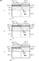
図3Aは、裏面型照射イメージセンサに採用される、本技術が適用された単位画素から構成される画素ユニット200の断面図である。ここでは説明の都合上、2色の単位画素、より具体的には緑用単位画素と赤用単位画素の組のみを図示するが、当然のことながら、これに限定されない。画素ユニット200を構成する単位画素には、それぞれ上下方向に複数層のカラーフィルタが離間して配置される。なお、以下の説明においては、1つの単位画素に対して、カラーフィルタが2層配置される場合について説明するが、配置されるカラーフィルタの数はこれに限定されない。
[Unit pixel to which this technology is applied]
FIG. 3A is a cross-sectional view of a
画素ユニット200においては、緑用フォトダイオード211−1及び赤用フォトダイオード211−2が隣接して配置されている。緑用フォトダイオード211−1の上には、緑用フィルタ部212−1及びオンチップレンズ213−1が下方から順に積層されている。また、赤用フォトダイオード211−2の上には、赤用フィルタ部212−2及びオンチップレンズ213−2が下方から順に積層されている。
In the
緑用フィルタ部212−1は、下方から順に、下段の緑用カラーフィルタ221−1、平坦化膜222の左側部分、及び上段の緑用カラーフィルタ223−1が積層されて構成される。赤用フィルタ部212−2は、下方から順に、下段の赤用カラーフィルタ221−2、平坦化膜222の右側部分、及び上段の赤用カラーフィルタ223−2が積層されて構成される。換言すると、緑用フィルタ部212−1と赤用フィルタ部212−2との組は、下方から順に、下段の緑用カラーフィルタ221−1と下段の赤用カラーフィルタ221−2との組、平坦化膜222、及び、上段の緑用カラーフィルタ223−1と上段の赤用カラーフィルタ223−2との組が積層されて構成される。なお、下段の緑用カラーフィルタ221−1と下段の赤用カラーフィルタ221−2との組は、それぞれ緑用フォトダイオード211−1及び赤用フォトダイオード211−2の直上か、若しくは可能な限り緑用フォトダイオード211−1及び赤用フォトダイオード211−2の近傍に配置される。また、下段の緑用カラーフィルタ221−1と上段の緑用カラーフィルタ223−1、下段の赤用カラーフィルタ221−2と上段の赤用カラーフィルタ223−2とは、それぞれ平坦化膜222がその間に配置されることにより、離間して配置される。
The green filter unit 212-1 is configured by laminating a lower green color filter 221-1, a left side portion of the
図3Aの例では、1つの単位画素に対して、カラーフィルタが2層配置される場合について説明したが、カラーフィルタが2層以上配置される場合には、対向する2層のカラーフィルタの組のうち、少なくとも1組の間が離間するように配置される。なお、対向する2層とは、最も近くに配置される2層、すなわち近接する2層を意味する。 In the example of FIG. 3A, the case where two layers of color filters are arranged for one unit pixel has been described. However, when two or more layers of color filters are arranged, a set of two layers of color filters facing each other is arranged. Of these, at least one set is disposed so as to be spaced apart. The two opposing layers mean the two layers arranged closest to each other, that is, the two adjacent layers.
図3Bは、カラーフィルタが3層配置された単位画素から構成される画素ユニット200eの断面図である。例えば、画素ユニット200eの緑用単位画素において、対向する2層のカラーフィルタの組とは、下段の緑用カラーフィルタ221−1aと中段の緑用カラーフィルタ224−1aとの組(以下、第1の組と称する)、及び、中段の緑用カラーフィルタ224−1aと上段の緑用カラーフィルタ223−1aとの組(以下、第2の組と称する)のことをいう。ここで、下段の緑用カラーフィルタ221−1aと上段の緑用カラーフィルタ223−1aとの組は、近接する2層ではないので、対向する2層のカラーフィルタの組ではない。
FIG. 3B is a cross-sectional view of a
図3Bに示される緑用単位画素においては、対向する2層のカラーフィルタの組、すなわち第1の組と第2の組は、どちらも2層のカラーフィルタの間が離間するように配置されているが、第1の組と第2の組のうちの少なくとも1組の間が離間するように配置されればよい。 In the unit pixel for green shown in FIG. 3B, two sets of color filters facing each other, that is, the first set and the second set are both arranged so that the two layers of color filters are separated from each other. However, what is necessary is just to arrange | position so that at least 1 set of 1st set and 2nd set may space apart.
ここで、下段の緑用カラーフィルタ221−1及び上段の緑用カラーフィルタ223−1の各々は、それぞれ同色のカラーフィルタであるとする。また、下段の赤用カラーフィルタ221−2及び上段の赤用カラーフィルタ223−2の各々は、それぞれ同色のカラーフィルタであるとする。ここで、同色とは、カラーフィルタの材料がもつ分光透過率特性が同一であるか、または分光透過率特性が異なっていても同色であることを意味する。画素ユニット200を構成する単位画素に配置されるカラーフィルタの色について図4を参照して説明する。
Here, it is assumed that each of the lower green color filter 221-1 and the upper green color filter 223-1 is the same color filter. Each of the lower red color filter 221-2 and the upper red color filter 223-2 is a color filter of the same color. Here, the same color means that the spectral transmittance characteristics of the color filter materials are the same or the same color even if the spectral transmittance characteristics are different. The color of the color filter arranged in the unit pixel constituting the
[単位画素に配置されるカラーフィルタの色]
図4は、画素ユニット200を構成する単位画素に配置されるカラーフィルタの分光透過率曲線を示す図である。図4において、縦軸は透過率を示し、横軸は波長を示している。
[Color filter color arranged in unit pixel]
FIG. 4 is a diagram showing a spectral transmittance curve of a color filter arranged in a unit pixel constituting the
図4Aに示されるように、点線で示される下段の緑用カラーフィルタ221−1及び上段の緑用カラーフィルタ223−1の特性は、同一の分光透過率を有しており、どちらも波長が520nm近辺で透過率が最も高くなる。また、実線で示される下段の赤用カラーフィルタ221−2及び上段の赤用カラーフィルタ223−2の特性は、同一の分光透過率を有しており、どちらも波長が600nm近辺で透過率が最も高くなる。すなわち、下段の緑用カラーフィルタ221−1及び上段の緑用カラーフィルタ223−1と、下段の赤用カラーフィルタ221−2及び上段の赤用カラーフィルタ223−2とは、それぞれ分光透過率特性が同一になるような材料からできている。このように、画素ユニット200を構成する単位画素に対して上下方向に配置される複数層のカラーフィルタは、図4Aに示されるように、それぞれ同一の分光透過率特性を有するものが採用される。
As shown in FIG. 4A, the characteristics of the lower green color filter 221-1 and the upper green color filter 223-1 indicated by dotted lines have the same spectral transmittance, both of which have a wavelength. The transmittance is highest around 520 nm. In addition, the characteristics of the lower red color filter 221-2 and the upper red color filter 223-2 indicated by the solid line have the same spectral transmittance, both of which have a transmittance of around 600 nm. Highest. That is, the lower green color filter 221-1 and the upper green color filter 223-1, and the lower red color filter 221-2 and the upper red color filter 223-2 have spectral transmittance characteristics, respectively. Are made of the same material. As described above, as shown in FIG. 4A, color filters having the same spectral transmittance characteristic are employed as the plurality of layers of color filters arranged in the vertical direction with respect to the unit pixel constituting the
また、図4Bに示されるように、一点鎖線で示される下段の緑用カラーフィルタ221−1の特性と点線で示される上段の緑用カラーフィルタ223−1の特性は、それぞれ異なる分光透過率を示しているが、どちらも波長が520nm近辺で透過率が最も高くなる。また、破線で示される下段の赤用カラーフィルタ221−2の特性と実線で示される上段の赤用カラーフィルタ223−2の特性は、それぞれ異なる分光透過率を示しているが、どちらも波長が600nm近辺で透過率が高くなる。すなわち、下段の緑用カラーフィルタ221−1及び上段の緑用カラーフィルタ223−1の特性と、下段の赤用カラーフィルタ221−2及び上段の赤用カラーフィルタ223−2の特性とは、それぞれ分光透過率特性が異なっていても同色である。 Further, as shown in FIG. 4B, the characteristics of the lower green color filter 221-1 indicated by the alternate long and short dash line and the characteristics of the upper green color filter 223-1 indicated by the dotted line have different spectral transmittances. As shown, in both cases, the transmittance is highest when the wavelength is around 520 nm. Further, the characteristic of the lower red color filter 221-2 indicated by a broken line and the characteristic of the upper red color filter 223-2 indicated by a solid line show different spectral transmittances, but both have different wavelengths. The transmittance increases around 600 nm. That is, the characteristics of the lower green color filter 221-1 and the upper green color filter 223-1 and the characteristics of the lower red color filter 221-2 and the upper red color filter 223-2 are respectively Even if the spectral transmittance characteristics are different, they are the same color.
ここでの同色とは、例えば、第1の色の単位画素のフォトダイオードの上方に配置される下段のカラーフィルタの分光透過率特性は、隣接する第2の色の単位画素のフォトダイオードの上方に配置される複数層のカラーフィルタの分光透過率特性よりも、第1の色の単位画素のフォトダイオードの上方に配置される上段のカラーフィルタの分光透過率特性に近似することを意味する。分光は、上下方向に配置された複数層のカラーフィルタの分光透過率の乗算により算出されるため、図4Bに示されるように、1つの単位画素に対して、分光透過率が異なっていても同色であるカラーフィルタが上下方向に複数層配置されることにより、分光形状の調整が可能となる。このように、画素ユニット200を構成する単位画素に対して上下方向に配置される複数層のカラーフィルタは、図4Bに示されるように、それぞれ異なる分光透過率特性を有していても同色であるものが採用される。
Here, the same color means, for example, that the spectral transmittance characteristic of the lower color filter disposed above the photodiode of the unit pixel of the first color is above the photodiode of the unit pixel of the adjacent second color. This means that the spectral transmittance characteristics of the upper color filter disposed above the photodiode of the unit pixel of the first color are approximated to the spectral transmittance characteristics of the multi-layer color filters disposed in the first color unit. Since the spectrum is calculated by multiplying the spectral transmittance of a plurality of layers of color filters arranged in the vertical direction, as shown in FIG. 4B, even if the spectral transmittance is different for one unit pixel. By arranging a plurality of color filters of the same color in the vertical direction, the spectral shape can be adjusted. As described above, the plurality of layers of color filters arranged in the vertical direction with respect to the unit pixel constituting the
このように、画素ユニット200において、1つの単位画素に対して上下方向に配置される複数層(図3Aの例では2層)のカラーフィルタは、それぞれ同色のカラーフィルタであるとする。
As described above, in the
図3Aの説明に戻り、オンチップレンズ213−1に入射された光は、上段の緑用カラーフィルタ223−1、平坦化膜222、及び下段の緑用カラーフィルタ221−1を透過して、緑用フォトダイオード211−1に集光され、入射する。より正確には、上段の緑用カラーフィルタ223−1において、オンチップレンズ213−1から射出された光のうち、緑色の波長帯域の光だけが透過し、平坦化膜222を透過する。さらに、下段の緑用カラーフィルタ221−1において、上段の緑用カラーフィルタ223−1及び平坦化膜222を透過した緑色の波長帯域の光だけが透過し、緑用フォトダイオード211−1に入射する。緑用フォトダイオード211−1は、入射した光の量、すなわち受光量に応じたレベルの電気信号を出力する。
Returning to the description of FIG. 3A, the light incident on the on-chip lens 213-1 is transmitted through the upper green color filter 223-1, the
オンチップレンズ213−2に入射された光は、同様の経路により、赤用フォトダイオード211−2に集光され、入射する。ただし、この場合、上段の赤用カラーフィルタ223−2及び下段の赤用カラーフィルタ221−2において、オンチップレンズ213−2から射出された光のうち、赤色の波長帯域の光だけが透過する点が異なる。 The light incident on the on-chip lens 213-2 is collected and incident on the red photodiode 211-2 through the same path. However, in this case, only the light in the red wavelength band of the light emitted from the on-chip lens 213-2 is transmitted through the upper red color filter 223-2 and the lower red color filter 221-2. The point is different.
このように、画素ユニット200を構成する単位画素には、それぞれ上下方向に複数層(図3Aの例では2層)の同色のカラーフィルタが離間して配置される。これにより、次の図5に示されるように、オンチップレンズとフォトダイオードとの間で発生する混色を低減することができる。
Thus, in the unit pixel constituting the
[画素ユニット200による混色の低減]
図5は、混色の低減について説明する図である。
[Reduction of color mixing by pixel unit 200]
FIG. 5 is a diagram for explaining the reduction of color mixing.
図5Aは、一般的な構成の画素ユニット10の断面図である。図5Aに示されるように、オンチップレンズ23−1から射出された光のうち、緑用カラーフィルタ32−1を透過した緑色の波長帯域の光の一部は、隣接する赤用フォトダイオード21−2へ漏れ込み、漏れ込んだ光が混色成分となって混色が発生する。
FIG. 5A is a cross-sectional view of the
これに対して、図5Bに示される本技術が適用された単位画素から構成される画素ユニット200においては、オンチップレンズ213−1から射出された光のうち、上段の緑用カラーフィルタ223−1を透過した緑色の波長帯域の光の一部は、赤用フォトダイオード211−2に漏れ込む前に下段の赤用カラーフィルタ221−2によりほぼ吸収されるので、赤用フォトダイオード211−2に入射する光は低減する。すなわち、下段の赤用カラーフィルタ221−2は、赤色の波長帯域の光だけを透過するので、上段の緑用カラーフィルタ223−1を透過した緑色の波長帯域の光は、下段の赤用カラーフィルタ221−2を透過せずにほぼ吸収される。したがって、本技術が適用された単位画素から構成される画素ユニット200によれば、図6に示されるように、混色を低減することができる。
On the other hand, in the
図6は、緑用カラーフィルタを透過した光が、赤用フォトダイオードに入射されて混色となる場合における、赤用フォトダイオードへの入射量を、カラーフィルタの透過率を用いて示す図である。図6において、縦軸は透過率を示し、横軸は波長を示している。 FIG. 6 is a diagram showing the amount of incidence on the red photodiode using the transmittance of the color filter when the light transmitted through the green color filter enters the red photodiode and is mixed. . In FIG. 6, the vertical axis indicates the transmittance, and the horizontal axis indicates the wavelength.
すなわち、所定の波長の光が、赤用フォトダイオードへ入射される量は、透過率が大きくなる程多くなる。したがって、緑色の光が赤用フォトダイオードへ漏れ込んで入射される量、換言すると赤用フォトダイオードにおいて発生する混色の影響度合は、520nm前後の波長帯域の透過率の大小により判定することができる。 That is, the amount of light having a predetermined wavelength incident on the red photodiode increases as the transmittance increases. Therefore, the amount of green light that leaks into and enters the red photodiode, in other words, the degree of influence of color mixing that occurs in the red photodiode, can be determined by the magnitude of the transmittance in the wavelength band around 520 nm. .
図6の実線は、緑用カラーフィルタの分光透過率曲線を示している。図1Aに示された一般的な構成の画素ユニット10においては、図6の実線の特性を有する緑用カラーフィルタ32−1の1層のみが設けられているため、図6の実線がそのまま、隣接する赤用フォトダイオード21−2に漏れ込んで入射される量、換言すると赤用フォトダイオードにおいて発生する混色の影響度合を示すことになる。
The solid line in FIG. 6 shows the spectral transmittance curve of the green color filter. In the
これに対して、本技術が適用された単位画素から構成される画素ユニット200において、上段の緑用カラーフィルタ223−1を透過した緑色の光は、下段の赤用カラーフィルタ221−2を透過した後に、赤用フォトダイオード211−2に入射される。ここで、上段の緑用カラーフィルタ223−1が図6の実線の特性を有し、下段の赤色用カラーフィルタ221−2が図4Bの破線で示される特性を有するものとすると、図6の実線と図4Bの破線とを合算した曲線、すなわち図6の点線が、上段の緑用カラーフィルタ223−1と下段の赤用カラーフィルタ221−2とを組み合わせた特性を示すことになる。この図6の点線が、本技術が適用された場合における、隣接する赤用フォトダイオード211−2に漏れ込んで入射される量、換言すると赤用フォトダイオードにおいて発生する混色の影響度合を示すことになる。
On the other hand, in the
従来についての図6の実線の特性と、本技術についての図6の点線の特性とを比較するに、520nm前後の波長帯域の透過率は、図6の点線の特性の方が圧倒的に低くなっている。このことは、本技術を適用した場合には、従来の場合と比較して、緑色の光が赤用フォトダイオードへ漏れ込んで入射される量、換言すると赤用フォトダイオードにおいて発生する混色の影響度合が圧倒的に低減されることを意味している。 Compared with the solid line characteristic of FIG. 6 for the conventional technique and the dotted line characteristic of FIG. 6 for the present technology, the transmittance in the wavelength band around 520 nm is overwhelmingly lower for the dotted line characteristic of FIG. It has become. This means that when this technology is applied, the amount of green light that leaks into and enters the red photodiode, in other words, the influence of color mixing that occurs in the red photodiode, compared to the conventional case. It means that the degree is overwhelmingly reduced.
これは、本技術の画素ユニット200においては、上段の緑用カラーフィルタ223−1を透過した緑色の光は、隣接する赤用フォトダイオード211−2に漏れ込む前に、下段の赤用カラーフィルタ221−2により吸収されるからである。
This is because in the
このように、画素ユニット200を構成する単位画素に対して、それぞれ上下方向に複数層の同色カラーフィルタが離間して配置されることにより、オンチップレンズとフォトダイオードとの間で発生する混色を低減することができることがわかる。
As described above, the unit color constituting the
[裏面型照射イメージセンサにおける画素ユニット200の製造処理]
次に、裏面型照射イメージセンサに採用される、画素ユニット200の製造処理について図7乃至図9を用いて説明する。
[Manufacturing Process of
Next, the manufacturing process of the
図7は、画素ユニット200を製造する製造装置230の機能的構成例を示すブロック図である。
FIG. 7 is a block diagram illustrating a functional configuration example of the
製造装置230は、形成部231及び塗布部232を有している。
The
形成部231は、配線層、カラーフィルタ、及びオンチップレンズを形成する。また、形成部232は、図15を参照して後述する半導体基板及び電極用の開口部を形成する。
The forming
塗布部232は、平坦化膜を塗布する。
The
図8は、裏面型照射イメージセンサにおける画素ユニット200の製造処理の流れを説明するフローチャートである。また、図9は、裏面型照射イメージセンサにおける画素ユニット200の製造処理の流れを示す図である。画素ユニット200の製造処理においては、適宜人手が介在したり、複数の装置により分担されて画素ユニット200が製造されることがあるが、本実施形態では説明を簡略化するために、1台の製造装置が、画素ユニット200を製造するまでの一連の処理を全て実行するものとする。
FIG. 8 is a flowchart for explaining the flow of the manufacturing process of the
ステップS1において、形成部231は、緑用フォトダイオード211−1及び赤用フォトダイオード211−2上に、配線層240を形成して、それを裏返す。この状態が、状態S1として示されている。
In step S <b> 1, the forming
ステップS2において、形成部231は、下段の緑用カラーフィルタ221−1を緑用フォトダイオード211−1の上方に形成する。この状態が、状態S2として示されている。なお、下段の緑用カラーフィルタ221−1は、カラーフィルタレジストの塗布及びリソグラフィにより形成される。
In step S2, the forming
ステップS3において、形成部231は、下段の赤用カラーフィルタ221−2を赤用フォトダイオード211−2の上方に形成する。すると、この状態が、状態S3として示されている。なお、下段の赤用カラーフィルタ221−2は、カラーフィルタレジストの塗布及びリソグラフィにより形成される。
In step S3, the forming
ステップS4において、塗布部232は、下段の緑用カラーフィルタ221−1と下段の赤用カラーフィルタ221−2との組の上方に、平坦化膜222を塗布する。この状態が、状態S4として示されている。
In step S <b> 4, the
ステップS5において、形成部231は、平坦化膜222の左側部分の上方に、上段の緑用カラーフィルタ223−1を形成する。この状態が、状態S5として示されている。なお、上段の緑用カラーフィルタ223−1は、カラーフィルタレジストの塗布及びリソグラフィにより形成される。
In step S <b> 5, the forming
ステップS6において、形成部231は、平坦化膜222の右側部分の上方に、上段の赤用カラーフィルタ223−2を形成する。この状態が、状態S6として示されている。なお、上段の赤用カラーフィルタ223−2は、カラーフィルタレジストの塗布及びリソグラフィにより形成される。
In step S <b> 6, the forming
ステップS7において、形成部231は、上段の緑用カラーフィルタ223−1と上段の赤用カラーフィルタ223−2との組の上方に、オンチップレンズ213−1とオンチップレンズ213−2をそれぞれ形成する。この状態が、状態S7として示されている。
In step S7, the forming
これにより、裏面型照射イメージセンサにおける画素ユニット200の製造処理は終了する。
Thereby, the manufacturing process of the
なお、ステップS4において、下段の緑用カラーフィルタ221−1と下段の赤用カラーフィルタ221−2との組の上方に塗布される平坦化膜222の厚みが調整されることにより、画素ユニット200の高さが調整される。ここで、画素ユニット200の高さに応じて、感度や混色及びシェーディングの度合いが変化する。したがって、感度が最も高く、混色及びシェーディングの発生が最も低減するような画素ユニット200の高さとなるように、平坦化膜222の厚みが調整されると好適である。
In step S4, the
[瞳補正の適用]
画素ユニット200を構成する単位画素に上下方向に配置される複数層の同色のカラーフィルタ、及びオンチップレンズに対して、瞳補正が加えられてもよい。瞳補正については、例えば特開2010−232595号公報等に記載されている。なお、以下に説明する画素ユニットは、図3Aの画素ユニット200と基本的に同様の構成をとるが、一部異なった構成をとる。そこで、以下の画素ユニットの構成の説明としては、図3Aの構成とは異なる構成の点についてのみ説明する。
[Apply pupil correction]
Pupil correction may be applied to a plurality of layers of the same color filter disposed in the vertical direction on the unit pixel constituting the
図10は、瞳補正が加えられた単位画素から構成される画素ユニットについて説明する図である。 FIG. 10 is a diagram illustrating a pixel unit including unit pixels to which pupil correction has been applied.
画素ユニット200cは、撮像素子260の中心部に配置される画素ユニットであり、画素ユニット200eは、撮像素子260の端部に配置される画素ユニットである。
The
撮像素子260の中心部に配置される画素ユニット200cにおいては、オンチップレンズ213−1cの中心軸方向から光が入射されるので、上段の緑用カラーフィルタ223−1c、平坦化膜222c、及び下段の緑用カラーフィルタ221−1cを透過した光は、緑用フォトダイオード211−1cに垂直に入射する。オンチップレンズ213−2cに入射された光も、同様に、赤用フォトダイオード211−2cに垂直に入射する。したがって、撮像素子260の中心部に配置される画素ユニット200cにおいては、オンチップレンズ213−1c及びオンチップレンズ213−2cと、緑用フィルタ部212−1c及び赤用フィルタ部212−2cには、瞳補正が加えられない。
In the
これに対して、斜め方向からの光が入射される撮像素子260の端部に配置される画素ユニット200eにおいては、オンチップレンズ213−1eの中心軸に対して斜め方向から光が入射されるので、上段の緑用カラーフィルタ223−1e、平坦化膜222e、及び下段の緑用カラーフィルタ221−1cを透過した光は、緑用フォトダイオード211−1eに斜めに入射する。オンチップレンズ213−2eに入射された光も、同様に、赤用フォトダイオード211−2eに斜めに入射する。すなわち、緑用フォトダイオード211−1e及び赤用フォトダイオード211−2eに対して入射光が効率よく集光されない。したがって、斜め方向から入射される光が効率よく集光されるように、オンチップレンズ213−1e及びオンチップレンズ213−2eと、緑用フィルタ部212−1e及び赤用フィルタ部212−2eには、光の入射角に応じた瞳補正が加えられる。
On the other hand, in the
すなわち、撮像素子260の中心部から端部に向かうにしたがって瞳補正量が大きくなるように、撮像素子260に配置された画素ユニット200に対して瞳補正が加えられる。また、画素ユニット200内においては、緑用フォトダイオード211−1及び赤用フォトダイオード211−2から離れた位置にある構成要素ほど瞳補正量が大きくなるように、オンチップレンズ213−1e及びオンチップレンズ213−2eと、緑用フィルタ部212−1及び赤用フィルタ部212−2に瞳補正が加えられる。具体的には、画素ユニット200eにおいては、下段の緑用カラーフィルタ221−1eと下段の赤用カラーフィルタ221−2eとの組、上段の緑用カラーフィルタ223−1eと上段の赤用カラーフィルタ223−2eとの組、オンチップレンズ213−1e及びオンチップレンズ213−2eとの組になるにつれて、瞳補正量が大きくなるように、画素ユニット200eに対して瞳補正が加えられる。なお、瞳補正量とは、フォトダイオードの中心を起点とした時のカラーフィルタ及びオンチップレンズのずらし量をいう。
That is, pupil correction is applied to the
このように、撮像素子260に配置される画素ユニット200を構成する単位画素のオンチップレンズ及びカラーフィルタに対して瞳補正が加えられることにより、撮像素子260は、画角端においても、感度が高く、混色の発生を低減することができる。
As described above, the pupil correction is applied to the on-chip lens and the color filter of the unit pixel constituting the
[カラーフィルタの数の変形例]
上述の例では、画素ユニットを構成する単位画素に配置される複数層のカラーフィルタは、どの色の単位画素に配置されるカラーフィルタも同数とされた。しかしながら、単位画素に配置される複数層のカラーフィルタは、色別にその数が変えられて配置されてもよい。
[Modification of number of color filters]
In the above-described example, the number of color filters arranged in the unit pixel of any color is the same as the number of color filters of the plurality of layers arranged in the unit pixel constituting the pixel unit. However, the plurality of layers of color filters arranged in the unit pixel may be arranged by changing the number for each color.
図11は、複数層のカラーフィルタの数が色別に変えられて配置される単位画素から構成される画素ユニットについて説明する図である。 FIG. 11 is a diagram for explaining a pixel unit composed of unit pixels arranged by changing the number of color filters in a plurality of layers for each color.
図11Aは、画素ユニット200fと、画素ユニット200fに隣接する画素ユニット200gの断面図である。
FIG. 11A is a cross-sectional view of the
図11Aに示されるように、画素ユニット200f,200gは、それぞれ平坦化膜222f,222gが厚く、オンチップレンズとフォトダイオードとの間の距離が長い。このような場合、1つの単位画素を超えて混色が発生するおそれがある。
As shown in FIG. 11A, in the
具体的には、図11Aに示されるように、オンチップレンズ213−2gから射出された光のうち、上段の赤用カラーフィルタ223−2gを透過した光の一部は、隣接する画素ユニット200fの赤用単位画素の赤用フォトダイオード211−2fへ漏れ込むおそれがある。すなわち、画素ユニット200gの赤用単位画素のオンチップレンズ213−2gから射出された光が、画素ユニット200gの緑用単位画素を飛びこえて、隣接する画素ユニット200fの赤用単位画素の赤用フォトダイオード211−2fへ漏れ込み、漏れ込んだ光が混色成分となって混色が発生するおそれがある。この場合、赤用単位画素の赤用フォトダイオード211−2fへ漏れ込む光が、赤用カラーフィルタ223−2gを透過した赤色の光(すなわち同色)であっても、解像度劣化等が生じるおそれがある。
Specifically, as shown in FIG. 11A, of the light emitted from the on-chip lens 213-2g, a part of the light transmitted through the upper red color filter 223-2g is adjacent to the
このようにして発生する混色を低減するために、画素ユニット200f,200gに配置される複数層のカラーフィルタの数を色別に増やす。
In order to reduce the color mixture that occurs in this way, the number of color filters in a plurality of layers arranged in the
図11Bは、複数層のカラーフィルタの数が色別に変えられて配置されている単位画素から構成される画素ユニット200fと、画素ユニット200fに隣接する画素ユニット200gの断面図である。図11Bに示されるように、画素ユニット200f,200gは、図11Aと比較して、それぞれ中段の緑用カラーフィルタ261−1f,261−1gがさらに配置されている。
FIG. 11B is a cross-sectional view of a
具体的には、図11Bに示されるように、画素ユニット200gの赤用単位画素のオンチップレンズ213−2gから射出された光のうち、上段の赤用カラーフィルタ223−2gを透過した赤色の波長帯域の光の一部は、隣接する画素ユニット200fの赤用単位画素の赤用フォトダイオード211−2fへ漏れ込むおそれがあったとしても、中段の緑用カラーフィルタ261−1gによりほぼ吸収される。したがって、隣接する画素ユニット200fの赤用単位画素の赤用フォトダイオード211−2fへ漏れ込む光は低減する。すなわち、中段の緑用カラーフィルタ261−1gは、緑色の波長帯域の光だけを透過するので、上段の赤用カラーフィルタ223−2gを透過した赤色の波長帯域の光は、中段の緑用カラーフィルタ261−1gを透過せずにほぼ吸収されるので、赤用フォトダイオード211−2fへ漏れ込む光は低減する。
Specifically, as shown in FIG. 11B, among the light emitted from the on-chip lens 213-2g of the red unit pixel of the
このように、画素ユニット200を構成する単位画素に配置されるカラーフィルタの数を、色別に変えることにより、1つの単位画素を超えて漏れ込む光による混色を低減することができる。なお、当然のことながら、他の色の単位画素のカラーフィルタの数が増やされてもよく、また配置されるカラーフィルタの数も上述の例に限定されない。
In this way, by changing the number of color filters arranged in the unit pixels constituting the
[カラーフィルタの数の他の変形例]
上述の例では、画素ユニットを構成する単位画素に配置される複数層のカラーフィルタは、全て複数層とされた。しかしながら、画素ユニットを構成する単位画素に配置されるカラーフィルタは、一部の色のカラーフィルタのみが複数層配置されてもよい。
[Other variations of the number of color filters]
In the above-described example, the plurality of layers of color filters arranged in the unit pixel constituting the pixel unit are all formed of a plurality of layers. However, as for the color filters arranged in the unit pixel constituting the pixel unit, only a part of the color filters of some colors may be arranged in a plurality of layers.
図12は、一部の色のカラーフィルタのみが複数層配置される単位画素から構成される画素ユニット200hの断面図である。図12に示されるように、緑用フィルタ部212−1hは、下方から順に、下段の緑用カラーフィルタ221−1h、平坦化膜222hの左側部分、及び上段の緑用カラーフィルタ223−1hが積層されて構成される。一方、赤用フィルタ部212−2hは、下方から順に、平坦化膜222hの右側部分及び上段の赤用カラーフィルタ223−2hが積層されて構成される。
FIG. 12 is a cross-sectional view of a
すなわち、画素ユニット200hのうち、赤用単位画素には、一般的な構成の単位画素と同様に赤用カラーフィルタ223−2hが1層のみ配置される。これに対して、緑用単位画素には、複数層の緑用カラーフィルタ221−1h,223−1hが配置される。この場合、赤用カラーフィルタ223−2hを透過した赤色の波長帯域の光のうち、緑用フォトダイオード211−1hに漏れ込む光を低減させることができる。これに対して、緑用カラーフィルタ223−1hを透過した緑色の波長帯域の光のうち、赤用フォトダイオード211−2hに漏れ込む光を低減させることは困難となる。
That is, in the
しかしながら、単位画素に配置するカラーフィルタの数を減らすことで画素ユニット200hの製造処理の工数を減らすことができるので、コストを抑制することができる。したがって、画素ユニットの設計者は、混色の量とコストの関係とのバランスを考えて、画素ユニットを構成する単位画素に配置するカラーフィルタの数を決定すると好適である。なお、当然のことながら、他の色の単位画素のカラーフィルタのみが複数層配置されてもよい。
However, since the number of man-hours for manufacturing the
[カラーフィルタの配置位置の例]
上述の例では、画素ユニットを構成する単位画素に配置されるカラーフィルタの位置は、フォトダイオードの直上とされた。しかしながら、単位画素のフォトダイオード上に段差ある場合などは、カラーフィルタの配置位置は、フォトダイオードの直上に限定されない。
[Example of color filter placement position]
In the above-described example, the position of the color filter arranged in the unit pixel constituting the pixel unit is directly above the photodiode. However, when there is a step on the photodiode of the unit pixel, the arrangement position of the color filter is not limited to just above the photodiode.
図13は、フォトダイオード上に段差がある場合の画素ユニットの断面図である。段差がある場合とは、例えば、フォトダイオード上に他の部品が配置されている場合等があり、図13の例では、画素ユニットのフォトダイオード上に金属遮光膜280乃至282が配置されている。
FIG. 13 is a cross-sectional view of the pixel unit when there is a step on the photodiode. The case where there is a step includes, for example, a case where other parts are arranged on the photodiode, and in the example of FIG. 13, the metal
したがって、図13Aに示されるように、はじめに画素ユニット200iの緑用フォトダイオード211−1i及び赤用フォトダイオード211−2i上に平坦化膜300iが塗布されて、緑用フォトダイオード211−1i及び赤用フォトダイオード211−2iの表面が平坦化される。その後、下段の緑用カラーフィルタ221−1iと下段の赤用カラーフィルタ221−2iとの組が配置されてもよい。
Therefore, as shown in FIG. 13A, the
また、図13Bに示されるように、画素ユニット200jのフォトダイオード上に配置された金属遮光膜280乃至282の間に、下段の緑用カラーフィルタ221−1jと下段の赤用カラーフィルタ221−2jとの組が配置されてもよい。具体的には、金属遮光膜280と金属遮光膜281の間に下段の緑用カラーフィルタ221−1jが配置され、金属遮光膜281と金属遮光膜282の間に下段の赤用カラーフィルタ221−2jが配置されてもよい。
As shown in FIG. 13B, the lower green color filter 221-1j and the lower red color filter 221-2j are disposed between the metal light-shielding
このように、画素ユニットを構成する単位画素のフォトダイオード上に段差がある場合であっても、複数層のカラーフィルタを配置することが可能である。これにより、混色を低減することができる。 Thus, even when there is a step on the photodiode of the unit pixel constituting the pixel unit, it is possible to arrange a plurality of layers of color filters. Thereby, color mixing can be reduced.
[ホワイト画素が適用される例]
上述の例では、画素ユニットは、例えば3色の単位画素、すなわち赤用単位画素、緑用単位画素、及び青用単位画素から構成されるとした。しかしながら、画素ユニットを構成する単位画素の色として、ホワイト用単位画素が適用されてもよい。ホワイト用単位画素については、例えば特開2009−296276号公報等に記載されている。ホワイト用単位画素は、フォトダイオード、透明なフィルタ、オンチップレンズ等の構成要素から構成される。なお、ホワイト用単位画素は、透明なフィルタを有さずに、カラーフィルタそのものを有さない構成であってもよい。図14の画素ユニットの例では、説明の都合上、緑用単位画素とホワイト用単位画素の組のみを図示する。
[Example where white pixels are applied]
In the above-described example, the pixel unit is composed of, for example, three color unit pixels, that is, a red unit pixel, a green unit pixel, and a blue unit pixel. However, a white unit pixel may be applied as the color of the unit pixel constituting the pixel unit. The white unit pixel is described in, for example, Japanese Unexamined Patent Application Publication No. 2009-296276. The unit pixel for white is composed of components such as a photodiode, a transparent filter, and an on-chip lens. The white unit pixel may have a configuration without the color filter itself without having a transparent filter. In the example of the pixel unit in FIG. 14, for convenience of explanation, only a set of green unit pixels and white unit pixels is illustrated.
図14は、ホワイト用単位画素が適用された画素ユニットについて説明する図である。 FIG. 14 is a diagram illustrating a pixel unit to which the white unit pixel is applied.
図14Aは、ホワイト用単位画素が配置された一般的な構成の画素ユニット10wの断面図である。画素ユニット10wにおいては、緑用フォトダイオード21−1w及びホワイト用フォトダイオード21−2wが隣接して配置されている。緑用フォトダイオード21−1wの上には、緑用フィルタ部22−1w及びオンチップレンズ23−1wが下方から順に積層されている。また、ホワイト用フォトダイオード21−2wの上には、ホワイト用フィルタ部22−2w及びオンチップレンズ23−2wが下方から順に積層されている。
FIG. 14A is a cross-sectional view of a
緑用フィルタ部22−1wは、下方から順に、平坦化膜31wの左側部分及び緑用カラーフィルタ32−1wが積層されて構成される。ホワイト用フィルタ部22−2wは、平坦化膜31wの右側部分から構成される。すなわち、ホワイト用フィルタ部22−2wは、カラーフィルタ自体を有さない構成である。
The green filter section 22-1w is configured by laminating the left side portion of the
図14Bは、ホワイト用単位画素が配置される本技術が適用された単位画素から構成される画素ユニット200wの断面図である。画素ユニット200wにおいては、緑用フォトダイオード211−1w及びホワイト用フォトダイオード211−2wが隣接して配置されている。緑用フォトダイオード211−1wの上には、緑用フィルタ部212−1w及びオンチップレンズ213−1wが下方から順に積層されている。また、ホワイト用フォトダイオード211−2wの上には、ホワイト用フィルタ部212−2w及びオンチップレンズ213−2wが下方から順に積層されている。
FIG. 14B is a cross-sectional view of a
緑用フィルタ部212−1wは、下方から順に、下段の緑用カラーフィルタ221−1w、平坦化膜222wの左側部分、及び上段の緑用カラーフィルタ223−1wが積層されて構成される。ホワイト用フィルタ部212−2wは、平坦化膜222wの右側部分から構成される。すなわち、ホワイト用フィルタ部212−2wは、カラーフィルタ自体を有さない構成である。
The green filter unit 212-1 w is configured by laminating a lower green color filter 221-1 w, a left side portion of the
図14Aに示されるように、ホワイト用単位画素が配置された一般的な構成の画素ユニット10wにおいては、オンチップレンズ23−2wから射出された赤色光,緑色光,青色光の一部は、隣接する緑用フォトダイオード21−1wへ漏れ込み、漏れ込んだ赤色光,緑色光,青色光が混色成分となって混色が発生する。
As shown in FIG. 14A, in a
これに対して、図14Bに示される本技術が適用された単位画素から構成される画素ユニット200wにおいては、オンチップレンズ213−2wから射出された赤色光,緑色光,青色光の一部は、隣接する緑用フォトダイオード211−1wに漏れ込む前に、赤色光と青色光は下段の緑用カラーフィルタ221−1wによりほぼ吸収され、緑色光のみが透過するので、緑用フォトダイオード211−2wに入射する光は低減する。すなわち、下段の緑用カラーフィルタ221−1wは、緑色の波長帯域の光だけを透過するので、オンチップレンズ213−2wから射出された赤色光,緑色光,青色光のうち、赤色光と青色光は、下段の緑用カラーフィルタ221−1wを透過せずに、ほぼ吸収される。すなわち、混色成分の量を低減することができる。したがって、本技術が適用された単位画素から構成される画素ユニット200wによれば、混色を低減することができる。なお、当然のことながら、緑色用単位画素以外の他の色の単位画素のカラーフィルタが複数層配置されてもよい。
On the other hand, in the
本技術は、CMOSイメージセンサまたはCCD(Charge Coupled Device)イメージセンサに配置される画素に適用することができる。また、本技術は、ベイヤ配列、クリアビット配列、またはその他の配列で配置される画素に対して適用することができる。また、本技術の単位画素に配置されるカラーフィルタの素材は、顔料系または染料系のどちらでもよい。また、本技術の単位画素は、裏面型照射イメージセンサに限らず、図15に示される表面型照射イメージセンサに適用することもできる。 The present technology can be applied to a pixel arranged in a CMOS image sensor or a CCD (Charge Coupled Device) image sensor. In addition, the present technology can be applied to pixels arranged in a Bayer array, a clear bit array, or other arrays. In addition, the material of the color filter disposed in the unit pixel of the present technology may be either pigment-based or dye-based. Further, the unit pixel of the present technology is not limited to the back-side illumination image sensor but can be applied to the front-side illumination image sensor shown in FIG.
[表面型照射イメージセンサに採用される本技術が適用された単位画素]
図15は、表面型照射イメージセンサに採用される単位画素の断面図である。なお、表面型照射イメージセンサについては、例えば特開2010−232595号公報、特開2010−41034号公報等に記載されている。
[Unit pixel to which this technology is applied to the surface irradiation image sensor]
FIG. 15 is a cross-sectional view of a unit pixel employed in a surface-type irradiation image sensor. The surface type irradiation image sensor is described in, for example, Japanese Patent Application Laid-Open Nos. 2010-232595 and 2010-41034.
図15Aは、表面型照射イメージセンサの撮像素子に採用される、一般的な構成の単位画素500の断面図である。単位画素500においては、半導体基板511、配線層512、フィルタ部513、及びオンチップレンズ514が下方から順に積層されている。
FIG. 15A is a cross-sectional view of a
半導体基板511には、フォトダイオード521が配置される。配線層512には、複数の配線531、導波路532、及び電極用の開口部533が含まれる。フィルタ部513は、下方から順に、平坦化膜541及びカラーフィルタ542が積層されて構成される。すなわち、単位画素500には、1種類のカラーフィルタ542が1層のみ配置される。
A
オンチップレンズ514に入射された光は、カラーフィルタ542及び平坦化膜541を透過して、導波路532を通過してフォトダイオード521に入射する。ここで、図示せぬ隣接する単位画素のオンチップレンズから射出された光のうち、図示せぬ隣接する単位画素のカラーフィルタを透過した光は、導波路532の上部に漏れ込み、漏れ込んだ光が導波路532を通過してフォトダイオード521に入射し、混色が発生する。混色は、S/Nや色再現性の低下の要因となるおそれがあることから、このような混色を低減するために、図15Bに示されるように、1つの単位画素に対して複数層のカラーフィルタを配置する。
The light incident on the on-
図15Bは、表面型照射イメージセンサに採用される、本技術が適用された単位画素560の断面図である。単位画素560においては、半導体基板571、配線層572、フィルタ部573、及びオンチップレンズ574が下方から順に積層されている。
FIG. 15B is a cross-sectional view of a
半導体基板571には、フォトダイオード581が配置される。配線層572には、複数の配線591、導波路592、及び電極用の開口部593が含まれる。フィルタ部573は、下方から順に、第1の平坦化膜601、下段のカラーフィルタ602、第2の平坦化膜603、及び上段のカラーフィルタ604が積層されて構成される。すなわち、単位画素560には、上下方向に複数層(図15Bの例では2層)の同色のカラーフィルタ、すなわち下段のカラーフィルタ602及び上段のカラーフィルタ604が配置される。
A
オンチップレンズ574に入射された光は、上段のカラーフィルタ604、第2の平坦化膜603、下段のカラーフィルタ602、及び第1の平坦化膜601を透過して、導波路592を通過してフォトダイオード581に入射する。
The light incident on the on-
単位画素560においては、図示せぬ隣接する単位画素のオンチップレンズから射出された光のうち、図示せぬ隣接する単位画素の上段のカラーフィルタを透過した光が、単位画素560に漏れ込んだとしても、漏れ込んだ光は下段のカラーフィルタ602によりほぼ吸収されるので、導波路592の上層への漏れ込みを低減でき、フォトダイオード581に入射する光は低減する。下段のカラーフィルタ602は、特定の第1の波長帯域の光だけを透過するので、図示せぬ隣接する単位画素のカラーフィルタを透過した特定の第2の波長帯域の光は、下段のカラーフィルタ602を透過せずに、ほぼ吸収される。したがって、本技術が適用された単位画素560によれば、混色を低減することができる。
In the
[表面型照射イメージセンサにおける画素ユニット560の製造処理]
次に、表面型照射イメージセンサの撮像素子に採用される、画素ユニット560の製造処理について図16,図17を用いて説明する。
[Manufacturing process of
Next, a manufacturing process of the
図16は、表面型照射イメージセンサにおける画素ユニット560の製造処理の流れを説明するフローチャートである。また、図17は、表面型照射イメージセンサにおける画素ユニット560の製造処理の流れを示す図である。画素ユニット560の製造処理においては、適宜人手が介在したり、複数の装置により分担されて画素ユニット560が製造されることがあるが、本実施形態では説明を簡略化するために、1台の製造装置230が、画素ユニット560を製造するまでの一連の処理を全て実行するものとする。
FIG. 16 is a flowchart for explaining the flow of the manufacturing process of the
ステップS21において、形成部231は、半導体基板571及び配線層572を形成する。ステップS22において、塗布部232は、配線層572の上方に第1の平坦化膜601を塗布する。ステップS23において、形成部231は、第1の平坦化膜601の上方に下段のカラーフィルタ602を形成する。この状態が、状態S21,S22,S23として示されている。
In step S <b> 21, the forming
ステップS24において、塗布部232は、下段のカラーフィルタ602の上方に、第2の平坦化膜603を塗布する。この状態が、状態S24として示されている。
In step S <b> 24, the
ステップS25において、形成部231は、第2の平坦化膜603の上方に上段のカラーフィルタ604を形成する。この状態が、状態S25として示されている。
In step S <b> 25, the
ステップS26において、形成部231は、上段のカラーフィルタ604の上方に、オンチップレンズ574を形成する。この状態が、状態S26として示されている。
In step S <b> 26, the forming
ステップS27において、形成部231は、電極用の開口部593を形成する。この状態が、状態S27として示されている。
In step S <b> 27, the forming
これにより、表面型照射イメージセンサにおける画素ユニット560の製造処理は終了する。
Thereby, the manufacturing process of the
以上、説明したように、1つの単位画素に対して、上下方向に複数層の同色のカラーフィルタを離間して配置することにより、オンチップレンズとフォトダイオードとの間で発生する混色を低減することができる。混色の低減により、高S/Nや高色再現性が実現可能となる。さらに、隣接画素からの光の漏れ込みが低減することにより、解像度の向上も可能となる。 As described above, color mixing that occurs between the on-chip lens and the photodiode is reduced by disposing a plurality of layers of the same color color filters apart in the vertical direction for one unit pixel. be able to. By reducing the color mixture, high S / N and high color reproducibility can be achieved. Furthermore, since the leakage of light from adjacent pixels is reduced, the resolution can be improved.
[撮像装置]
図18は、以上説明した本技術を適用した画素ユニットから構成される撮像素子を搭載した撮像装置、すなわち、本技術を適用した撮像装置の主な構成例を示すブロック図である。
[Imaging device]
FIG. 18 is a block diagram illustrating an example of a main configuration of an imaging device including an imaging device including a pixel unit to which the present technology described above is applied, that is, an imaging device to which the present technology is applied.
図18に示されるように、撮像装置700は、レンズ部711、撮像素子712、操作部713、制御部714、画像処理部715、表示部716、コーデック処理部717、および記録部718を有する。
As illustrated in FIG. 18, the
レンズ部711は、被写体までの焦点を調整し、焦点が合った位置からの光を集光し、撮像素子712に供給する。
The
撮像素子712は、フィルタ部731及び画素部732、並びに画素信号読み出し部733から構成される。
The
フィルタ部731及び画素部732は、上述した本技術が適用された複数の画素ユニット200(図3参照)の集合体である。すなわち、画素ユニット200の観点からすると、オンチップレンズ213−1及び緑用フィルタ部212−1、並びにオンチップレンズ213−2及び赤用フィルタ部212−2が、フィルタ部731の一部を構成する。緑用フォトダイオード211−1及び赤用フォトダイオード211−2が、画素部732の一部を構成する。換言すると、各画素ユニット200の各々についてのオンチップレンズ213−1及び緑用フィルタ部212−2、並びにオンチップレンズ213−2及び赤用フィルタ部212−2の集合体が、フィルタ部731を構成する。各画素ユニット200の各々についての緑用フォトダイオード211−1及び赤用フォトダイオード211−2の集合体が、画素部732を構成する。
The
画素部732は、レンズ711及びフィルタ部731を介して入射される光を受光し、これを光電変換して光の強度に応じた電圧信号(アナログ信号)を出力する。画素信号読み出し部733は、画素部732から画素毎のアナログ信号を画素信号として読み出して、A/D(Analog/Digital)変換を施してデジタル信号となった画素信号を画像処理部715に供給する。
The
操作部713は、例えば、ジョグダイヤル(商標)、キー、ボタン、またはタッチパネル等により構成され、ユーザによる操作入力を受け、その操作入力に対応する信号を制御部714に供給する。
The
制御部714は、操作部713により入力されたユーザの操作入力に対応する信号に基づいて、レンズ部711、撮像素子712、画像処理部715、表示部716、コーデック処理部717、および記録部718を制御する。
Based on the signal corresponding to the user's operation input input by the
画像処理部715は、撮像素子712から供給された画像信号に対して、例えば、ホワイトバランス調整、デモザイク処理、マトリックス処理、ガンマ補正、およびYC変換等の各種画像処理を施し、表示部716およびコーデック処理部717に供給する。
The
表示部716は、例えば、液晶ディスプレイ等として構成され、画像処理部715からの画像信号に基づいて、被写体の画像を表示する。
The
コーデック処理部717は、画像処理部715からの画像信号に対して、所定の方式の符号化処理を施し、符号化処理の結果得られた画像データを記録部718に供給する。
The
記録部718は、コーデック処理部717からの画像データを記録する。記録部718に記録された画像データは、必要に応じて画像処理部715に読み出されることで、表示部716に供給され、対応する画像が表示される。
The
なお、本技術を適用した固体撮像素子を備える撮像装置は、上述した構成に限らず、他の構成であってもよい。 Note that the imaging apparatus including the solid-state imaging element to which the present technology is applied is not limited to the configuration described above, and may have another configuration.
また、以上において、1つの装置(または処理部)として説明した構成が、複数の装置(または処理部)として構成されるようにしてもよい。逆に、以上において複数の装置(または処理部)として説明した構成が、まとめて1つの装置(または処理部)として構成されるようにしてもよい。また、各装置(または各処理部)の構成に上述した以外の構成が付加されるようにしてももちろんよい。さらに、システム全体としての構成や動作が実質的に同じであれば、ある装置(または処理部)の構成の一部が他の装置(または他の処理部)の構成に含まれるようにしてもよい。つまり、本技術の実施の形態は、上述した実施の形態に限定されるものではなく、本技術の要旨を逸脱しない範囲において種々の変更が可能である。 In addition, in the above description, the configuration described as one device (or processing unit) may be configured as a plurality of devices (or processing units). Conversely, the configuration described above as a plurality of devices (or processing units) may be configured as a single device (or processing unit). Of course, a configuration other than that described above may be added to the configuration of each device (or each processing unit). Further, if the configuration and operation of the entire system are substantially the same, a part of the configuration of a certain device (or processing unit) may be included in the configuration of another device (or other processing unit). Good. That is, the embodiments of the present technology are not limited to the above-described embodiments, and various modifications can be made without departing from the gist of the present technology.
本技術は、撮像素子または撮像装置に適用することができる。 The present technology can be applied to an imaging element or an imaging apparatus.
200 画素ユニット, 211−1,211−2 フォトダイオード, 212−1,212−2 フィルタ部, 213−1,213−2 オンチップレンズ, 221−1 下段の緑用カラーフィルタ, 221−2 下段の赤用カラーフィルタ, 223−1 上段の緑用カラーフィルタ, 223−2 上段の赤用カラーフィルタ, 240 配線層, 712 撮像素子, 731 フィルタ部, 732 画素部, 733 画素読み出し部 200 pixel units, 211-1, 211-2 photodiode, 212-1, 212-2 filter section, 213-1, 212-2 on-chip lens, 221-1 lower green color filter, 221-2 lower Red color filter, 223-1 Upper green color filter, 223-2 Upper red color filter, 240 Wiring layer, 712 Image sensor, 731 Filter unit, 732 pixel unit, 733 pixel readout unit
Claims (8)
前記フォトダイオード部の少なくとも一部と対向する第1のカラーフィルタと、前記第1のカラーフィルタと対向する前記第1のカラーフィルタと同色の第2のカラーフィルタと
を含む第1の単位画素と、
光を受光する前記フォトダイオード部と異なる他のフォトダイオード部と、
前記他のフォトダイオード部の少なくとも一部と対向する前記第1および第2のカラーフィルタと異色の第3のカラーフィルタと
を含む前記第1の単位画素に隣接する第2の単位画素とを備え、
前記第1のカラーフィルタと前記第2のカラーフィルタとは離間しており、かつ、それぞれ異なる分光透過率特性を有しており、
前記第1のカラーフィルタと前記第2のカラーフィルタがそれぞれ有する分光透過率特性の波形が近似する程度を示す類似度は、前記第1のカラーフィルタと前記第2の単位画素に含まれる前記第3のカラーフィルタがそれぞれ有する分光透過率特性の類似度よりも高く、前記第2のカラーフィルタと前記第2の単位画素に含まれる前記第3のカラーフィルタがそれぞれ有する分光透過率特性の類似度よりも高く、
前記第1の単位画素は、前記第1のカラーフィルタと前記第2のカラーフィルタを含むN枚のカラーフィルタを有し、
前記第2の単位画素は、前記第3のカラーフィルタを含むM枚のカラーフィルタを有し、
前記Nは2以上の整数値であり、前記Mは前記Nとは異なる1以上の整数値であり、かつ、前記Nは、前記Mより大きく、
前記第1の単位画素は、複数の色の単位画素からなる画素ユニットのうち最も数の多い色の単位画素であり、前記第2の単位画素は、前記第1の単位画素以外の色の単位画素である
撮像素子。 A photodiode portion for receiving light;
A first unit pixel including: a first color filter facing at least a part of the photodiode portion; and a second color filter having the same color as the first color filter facing the first color filter; ,
Another photodiode part different from the photodiode part for receiving light; and
A second unit pixel adjacent to the first unit pixel including the first and second color filters opposed to at least a part of the other photodiode portion and a third color filter having a different color. ,
The first color filter and the second color filter are separated from each other and have different spectral transmittance characteristics,
The similarity indicating the degree to which the waveforms of the spectral transmittance characteristics possessed by the first color filter and the second color filter are approximated is the first color filter and the second unit pixel included in the second unit pixel. The similarity of the spectral transmittance characteristics of the second color filter and the third color filter included in the second unit pixel is higher than the similarity of the spectral transmittance characteristics of the three color filters. Higher than
The first unit pixel has N color filters including the first color filter and the second color filter,
The second unit pixel has M color filters including the third color filter,
Wherein N is an integer of 2 or more values, wherein M is Ri 1 or more integer values Der different from the N, and wherein N is greater than the M,
The first unit pixel is a unit pixel of a color having the largest number among pixel units including unit pixels of a plurality of colors, and the second unit pixel is a unit of a color other than the first unit pixel. An image sensor that is a pixel .
請求項1に記載の撮像素子。 The imaging device according to claim 1.
請求項2に記載の撮像素子。 The imaging device according to claim 2.
前記第3のカラーフィルタと同色で、かつ、離間している第4のカラーフィルタをさらに含む
請求項1乃至3のいずれかに記載の撮像素子。 The second unit pixel is
The third color filter and the same color, and image sensor according to any one of claims 1 to 3 further comprising a fourth color filter that are spaced apart.
さらに、光を集光するオンチップレンズをそれぞれ含む
請求項1乃至4のいずれかに記載の撮像素子。 Each of the first unit pixel and the second unit pixel is:
The imaging device according to the on-chip lens that collects light to any one of claims 1 to 4 comprising respectively.
請求項1乃至5のいずれかに記載の撮像素子。 The first color filter, the image pickup device according to any one of claims 1 to 5 is disposed immediately above the photodiode portion.
前記第1のカラーフィルタは、前記平坦化膜の上に配置される
請求項1乃至6のいずれかに記載の撮像素子。 A planarizing film is applied on the photodiode portion,
The first color filter, the image pickup device according to any one of claims 1 to 6 is disposed on the planarizing film.
前記第1のカラーフィルタは、前記導波路の上に配置される
請求項1乃至7のいずれかに記載の撮像素子。 A waveguide is formed on the photodiode part,
The first color filter, the image pickup device according to any one of claims 1 to 7 is placed on top of the waveguide.
Priority Applications (7)
| Application Number | Priority Date | Filing Date | Title |
|---|---|---|---|
| JP2011166382A JP6080343B2 (en) | 2011-07-29 | 2011-07-29 | Image sensor and manufacturing method thereof |
| KR1020147001187A KR102048592B1 (en) | 2011-07-29 | 2012-07-20 | Imaging element and method for manufacturing same |
| EP12819555.9A EP2738811B1 (en) | 2011-07-29 | 2012-07-20 | Imaging element and method for manufacturing same |
| PCT/JP2012/068417 WO2013018559A1 (en) | 2011-07-29 | 2012-07-20 | Imaging element and method for manufacturing same |
| CN201280034909.8A CN103650143B (en) | 2011-07-29 | 2012-07-20 | Image-forming component and manufacture method thereof |
| KR1020197033901A KR102153848B1 (en) | 2011-07-29 | 2012-07-20 | Imaging element and method for manufacturing same |
| US14/233,226 US9380277B2 (en) | 2011-07-29 | 2012-07-20 | Imaging device with reduced color mixing and method of manufacturing the same |
Applications Claiming Priority (1)
| Application Number | Priority Date | Filing Date | Title |
|---|---|---|---|
| JP2011166382A JP6080343B2 (en) | 2011-07-29 | 2011-07-29 | Image sensor and manufacturing method thereof |
Related Child Applications (1)
| Application Number | Title | Priority Date | Filing Date |
|---|---|---|---|
| JP2015231325A Division JP6126190B2 (en) | 2015-11-27 | 2015-11-27 | Image sensor |
Publications (3)
| Publication Number | Publication Date |
|---|---|
| JP2013030652A JP2013030652A (en) | 2013-02-07 |
| JP2013030652A5 JP2013030652A5 (en) | 2014-09-11 |
| JP6080343B2 true JP6080343B2 (en) | 2017-02-15 |
Family
ID=47629087
Family Applications (1)
| Application Number | Title | Priority Date | Filing Date |
|---|---|---|---|
| JP2011166382A Active JP6080343B2 (en) | 2011-07-29 | 2011-07-29 | Image sensor and manufacturing method thereof |
Country Status (6)
| Country | Link |
|---|---|
| US (1) | US9380277B2 (en) |
| EP (1) | EP2738811B1 (en) |
| JP (1) | JP6080343B2 (en) |
| KR (2) | KR102153848B1 (en) |
| CN (1) | CN103650143B (en) |
| WO (1) | WO2013018559A1 (en) |
Families Citing this family (2)
| Publication number | Priority date | Publication date | Assignee | Title |
|---|---|---|---|---|
| WO2016103430A1 (en) * | 2014-12-25 | 2016-06-30 | キヤノン株式会社 | Line sensor, image reading device, image formation device |
| US20220367548A1 (en) * | 2021-05-17 | 2022-11-17 | Omnivision Technologies, Inc. | Crosstalk-suppressing image sensor |
Family Cites Families (21)
| Publication number | Priority date | Publication date | Assignee | Title |
|---|---|---|---|---|
| JPH02285674A (en) | 1989-04-26 | 1990-11-22 | Toppan Printing Co Ltd | Color filter and solid-state image sensing device |
| JP2951942B1 (en) * | 1998-05-26 | 1999-09-20 | 松下電子工業株式会社 | Method for manufacturing solid-state imaging device |
| JP2002184965A (en) | 2000-12-15 | 2002-06-28 | Sony Corp | Color solid-state image pickup chip and manufacturing method thereof |
| US7248297B2 (en) * | 2001-11-30 | 2007-07-24 | The Board Of Trustees Of The Leland Stanford Junior University | Integrated color pixel (ICP) |
| JP2006033493A (en) * | 2004-07-16 | 2006-02-02 | Matsushita Electric Ind Co Ltd | Imaging apparatus |
| EP1812968B1 (en) * | 2004-08-25 | 2019-01-16 | Callahan Cellular L.L.C. | Apparatus for multiple camera devices and method of operating same |
| JP4793042B2 (en) | 2005-03-24 | 2011-10-12 | ソニー株式会社 | Solid-state imaging device and imaging apparatus |
| JP2007294552A (en) * | 2006-04-23 | 2007-11-08 | Nikon Corp | Solid-state imaging device |
| US20080090323A1 (en) * | 2006-10-12 | 2008-04-17 | United Microelectronics Corp. | Image sensor and method of fabricating the same |
| JP4349456B2 (en) * | 2006-10-23 | 2009-10-21 | ソニー株式会社 | Solid-state image sensor |
| JP2008288243A (en) * | 2007-05-15 | 2008-11-27 | Sony Corp | Solid-state imaging device, manufacturing method thereof and imaging device |
| JP5076679B2 (en) * | 2007-06-28 | 2012-11-21 | ソニー株式会社 | Solid-state imaging device and camera module |
| US7675024B2 (en) * | 2008-04-23 | 2010-03-09 | Aptina Imaging Corporation | Method and apparatus providing color filter array with non-uniform color filter sizes |
| JP2009296276A (en) | 2008-06-04 | 2009-12-17 | Sony Corp | Imaging device and camera |
| JP5446484B2 (en) | 2008-07-10 | 2014-03-19 | ソニー株式会社 | Solid-state imaging device, manufacturing method thereof, and imaging device |
| JP5428451B2 (en) | 2009-03-30 | 2014-02-26 | ソニー株式会社 | Solid-state imaging device, manufacturing method thereof, and imaging device |
| JP4770928B2 (en) * | 2009-01-13 | 2011-09-14 | ソニー株式会社 | Optical element and solid-state image sensor |
| JP2010258104A (en) * | 2009-04-22 | 2010-11-11 | Panasonic Corp | Solid-state imaging element |
| JP2010278272A (en) * | 2009-05-29 | 2010-12-09 | Panasonic Corp | Solid-state imaging element and method of manufacturing solid-state imaging element |
| JP2011040454A (en) * | 2009-08-07 | 2011-02-24 | Sony Corp | Solid-state imaging device, method for manufacturing the solid-state imaging device, and electronic apparatus |
| JP2011049203A (en) * | 2009-08-25 | 2011-03-10 | Toppan Printing Co Ltd | Method of manufacturing solid-state imaging element |
-
2011
- 2011-07-29 JP JP2011166382A patent/JP6080343B2/en active Active
-
2012
- 2012-07-20 KR KR1020197033901A patent/KR102153848B1/en active IP Right Grant
- 2012-07-20 WO PCT/JP2012/068417 patent/WO2013018559A1/en active Application Filing
- 2012-07-20 US US14/233,226 patent/US9380277B2/en active Active
- 2012-07-20 KR KR1020147001187A patent/KR102048592B1/en active IP Right Grant
- 2012-07-20 CN CN201280034909.8A patent/CN103650143B/en active Active
- 2012-07-20 EP EP12819555.9A patent/EP2738811B1/en not_active Not-in-force
Also Published As
| Publication number | Publication date |
|---|---|
| EP2738811A1 (en) | 2014-06-04 |
| EP2738811A4 (en) | 2015-04-01 |
| KR20190133271A (en) | 2019-12-02 |
| CN103650143A (en) | 2014-03-19 |
| US20140146206A1 (en) | 2014-05-29 |
| KR102048592B1 (en) | 2020-01-22 |
| EP2738811B1 (en) | 2018-10-17 |
| WO2013018559A1 (en) | 2013-02-07 |
| JP2013030652A (en) | 2013-02-07 |
| KR102153848B1 (en) | 2020-09-08 |
| US9380277B2 (en) | 2016-06-28 |
| CN103650143B (en) | 2016-10-26 |
| KR20140053961A (en) | 2014-05-08 |
Similar Documents
| Publication | Publication Date | Title |
|---|---|---|
| TWI460520B (en) | Solid-state imaging device and camera module | |
| JP6789820B2 (en) | Solid-state image sensor, its manufacturing method, and electronic equipment | |
| JP5074106B2 (en) | Solid-state image sensor and camera | |
| US9294691B2 (en) | Imaging device, imaging apparatus, manufacturing apparatus and manufacturing method | |
| JP5538553B2 (en) | Solid-state imaging device and imaging apparatus | |
| JP2013021168A (en) | Solid-state imaging device, manufacturing method of solid-state imaging device, and electronic apparatus | |
| JP5774502B2 (en) | Solid-state imaging device | |
| WO2010100692A1 (en) | Solid-state imaging device, imaging module, and imaging system | |
| JP2012023137A (en) | Solid state imaging device and method of manufacturing the same | |
| JP2013046013A (en) | Solid-state imaging device and electronic apparatus | |
| WO2013099151A1 (en) | Solid-state imaging element, imaging device, and signal processing method | |
| JP6080343B2 (en) | Image sensor and manufacturing method thereof | |
| JP2003258220A (en) | Imaging element and imaging device | |
| JP2007047569A (en) | Microlens device, solid state image pickup element, display device, and electronic information equipment | |
| JP6126190B2 (en) | Image sensor | |
| JP2013118295A (en) | Method of manufacturing solid state image sensor, solid state image sensor, and electronic information apparatus | |
| TWI253597B (en) | Solid-state image sensor for improving sensing quality and manufacturing method thereof | |
| JP2018139394A (en) | Imaging device | |
| JP2016197794A (en) | Imaging device | |
| JP2013090085A (en) | Image pickup device and image processing method and program | |
| JP2007288107A (en) | Solid imaging device and camera | |
| JP2014086743A (en) | Solid-state image sensor, imaging apparatus and signal processing method | |
| JP2014086742A (en) | Solid-state image sensor, imaging apparatus and signal processing method |
Legal Events
| Date | Code | Title | Description |
|---|---|---|---|
| A521 | Request for written amendment filed |
Free format text: JAPANESE INTERMEDIATE CODE: A523 Effective date: 20140723 |
|
| A621 | Written request for application examination |
Free format text: JAPANESE INTERMEDIATE CODE: A621 Effective date: 20140723 |
|
| A131 | Notification of reasons for refusal |
Free format text: JAPANESE INTERMEDIATE CODE: A131 Effective date: 20150122 |
|
| A521 | Request for written amendment filed |
Free format text: JAPANESE INTERMEDIATE CODE: A523 Effective date: 20150313 |
|
| A02 | Decision of refusal |
Free format text: JAPANESE INTERMEDIATE CODE: A02 Effective date: 20150901 |
|
| A521 | Request for written amendment filed |
Free format text: JAPANESE INTERMEDIATE CODE: A523 Effective date: 20151127 |
|
| A911 | Transfer to examiner for re-examination before appeal (zenchi) |
Free format text: JAPANESE INTERMEDIATE CODE: A911 Effective date: 20151204 |
|
| A912 | Re-examination (zenchi) completed and case transferred to appeal board |
Free format text: JAPANESE INTERMEDIATE CODE: A912 Effective date: 20160219 |
|
| A711 | Notification of change in applicant |
Free format text: JAPANESE INTERMEDIATE CODE: A712 Effective date: 20160720 |
|
| A521 | Request for written amendment filed |
Free format text: JAPANESE INTERMEDIATE CODE: A523 Effective date: 20161121 |
|
| A61 | First payment of annual fees (during grant procedure) |
Free format text: JAPANESE INTERMEDIATE CODE: A61 Effective date: 20170117 |
|
| R150 | Certificate of patent or registration of utility model |
Ref document number: 6080343 Country of ref document: JP Free format text: JAPANESE INTERMEDIATE CODE: R150 |
|
| R250 | Receipt of annual fees |
Free format text: JAPANESE INTERMEDIATE CODE: R250 |