JP6079980B2 - Rapid thermal processing chamber with micropositioning system - Google Patents
Rapid thermal processing chamber with micropositioning system Download PDFInfo
- Publication number
- JP6079980B2 JP6079980B2 JP2011534920A JP2011534920A JP6079980B2 JP 6079980 B2 JP6079980 B2 JP 6079980B2 JP 2011534920 A JP2011534920 A JP 2011534920A JP 2011534920 A JP2011534920 A JP 2011534920A JP 6079980 B2 JP6079980 B2 JP 6079980B2
- Authority
- JP
- Japan
- Prior art keywords
- substrate
- substrate support
- support
- chamber
- edge ring
- Prior art date
- Legal status (The legal status is an assumption and is not a legal conclusion. Google has not performed a legal analysis and makes no representation as to the accuracy of the status listed.)
- Active
Links
- 238000012545 processing Methods 0.000 title claims description 51
- 239000000758 substrate Substances 0.000 claims description 502
- 238000010438 heat treatment Methods 0.000 claims description 17
- 239000007788 liquid Substances 0.000 claims description 6
- 238000000034 method Methods 0.000 description 28
- 235000012431 wafers Nutrition 0.000 description 25
- 230000007246 mechanism Effects 0.000 description 19
- 230000003287 optical effect Effects 0.000 description 16
- 238000001816 cooling Methods 0.000 description 13
- 239000000463 material Substances 0.000 description 12
- 230000008569 process Effects 0.000 description 12
- 239000007789 gas Substances 0.000 description 10
- 239000003507 refrigerant Substances 0.000 description 10
- LYCAIKOWRPUZTN-UHFFFAOYSA-N Ethylene glycol Chemical compound OCCO LYCAIKOWRPUZTN-UHFFFAOYSA-N 0.000 description 9
- 238000004891 communication Methods 0.000 description 8
- XEEYBQQBJWHFJM-UHFFFAOYSA-N Iron Chemical compound [Fe] XEEYBQQBJWHFJM-UHFFFAOYSA-N 0.000 description 4
- 238000000429 assembly Methods 0.000 description 4
- 230000000712 assembly Effects 0.000 description 4
- 238000009826 distribution Methods 0.000 description 4
- 239000012530 fluid Substances 0.000 description 4
- 238000005259 measurement Methods 0.000 description 4
- 238000012546 transfer Methods 0.000 description 4
- 230000000007 visual effect Effects 0.000 description 4
- IJGRMHOSHXDMSA-UHFFFAOYSA-N Atomic nitrogen Chemical compound N#N IJGRMHOSHXDMSA-UHFFFAOYSA-N 0.000 description 3
- 238000004458 analytical method Methods 0.000 description 3
- 238000001514 detection method Methods 0.000 description 3
- 239000001307 helium Substances 0.000 description 3
- 229910052734 helium Inorganic materials 0.000 description 3
- SWQJXJOGLNCZEY-UHFFFAOYSA-N helium atom Chemical compound [He] SWQJXJOGLNCZEY-UHFFFAOYSA-N 0.000 description 3
- 230000001939 inductive effect Effects 0.000 description 3
- PXHVJJICTQNCMI-UHFFFAOYSA-N nickel Substances [Ni] PXHVJJICTQNCMI-UHFFFAOYSA-N 0.000 description 3
- 239000010453 quartz Substances 0.000 description 3
- 230000004044 response Effects 0.000 description 3
- VYPSYNLAJGMNEJ-UHFFFAOYSA-N silicon dioxide Inorganic materials O=[Si]=O VYPSYNLAJGMNEJ-UHFFFAOYSA-N 0.000 description 3
- XLYOFNOQVPJJNP-UHFFFAOYSA-N water Substances O XLYOFNOQVPJJNP-UHFFFAOYSA-N 0.000 description 3
- 230000008859 change Effects 0.000 description 2
- 239000002826 coolant Substances 0.000 description 2
- 239000012636 effector Substances 0.000 description 2
- 230000006870 function Effects 0.000 description 2
- 238000005286 illumination Methods 0.000 description 2
- 238000005468 ion implantation Methods 0.000 description 2
- 229910052742 iron Inorganic materials 0.000 description 2
- 238000004519 manufacturing process Methods 0.000 description 2
- 238000012986 modification Methods 0.000 description 2
- 230000004048 modification Effects 0.000 description 2
- 230000005855 radiation Effects 0.000 description 2
- 239000010935 stainless steel Substances 0.000 description 2
- 229910001220 stainless steel Inorganic materials 0.000 description 2
- 239000000725 suspension Substances 0.000 description 2
- 238000007669 thermal treatment Methods 0.000 description 2
- RYGMFSIKBFXOCR-UHFFFAOYSA-N Copper Chemical compound [Cu] RYGMFSIKBFXOCR-UHFFFAOYSA-N 0.000 description 1
- 229910001209 Low-carbon steel Inorganic materials 0.000 description 1
- XUIMIQQOPSSXEZ-UHFFFAOYSA-N Silicon Chemical compound [Si] XUIMIQQOPSSXEZ-UHFFFAOYSA-N 0.000 description 1
- 238000010521 absorption reaction Methods 0.000 description 1
- XAGFODPZIPBFFR-UHFFFAOYSA-N aluminium Chemical compound [Al] XAGFODPZIPBFFR-UHFFFAOYSA-N 0.000 description 1
- 229910052782 aluminium Inorganic materials 0.000 description 1
- 239000003990 capacitor Substances 0.000 description 1
- 229910010293 ceramic material Inorganic materials 0.000 description 1
- 238000004140 cleaning Methods 0.000 description 1
- 239000011248 coating agent Substances 0.000 description 1
- 238000000576 coating method Methods 0.000 description 1
- 229910052802 copper Inorganic materials 0.000 description 1
- 239000010949 copper Substances 0.000 description 1
- 230000008878 coupling Effects 0.000 description 1
- 238000010168 coupling process Methods 0.000 description 1
- 238000005859 coupling reaction Methods 0.000 description 1
- 238000013461 design Methods 0.000 description 1
- 238000007667 floating Methods 0.000 description 1
- 238000010191 image analysis Methods 0.000 description 1
- 238000011065 in-situ storage Methods 0.000 description 1
- 238000002347 injection Methods 0.000 description 1
- 239000007924 injection Substances 0.000 description 1
- 238000005339 levitation Methods 0.000 description 1
- 239000000696 magnetic material Substances 0.000 description 1
- 238000012544 monitoring process Methods 0.000 description 1
- 229910052759 nickel Inorganic materials 0.000 description 1
- 239000013307 optical fiber Substances 0.000 description 1
- 239000002245 particle Substances 0.000 description 1
- 230000002093 peripheral effect Effects 0.000 description 1
- 238000007747 plating Methods 0.000 description 1
- 229920000642 polymer Polymers 0.000 description 1
- 230000009467 reduction Effects 0.000 description 1
- 239000000523 sample Substances 0.000 description 1
- 229910052594 sapphire Inorganic materials 0.000 description 1
- 239000010980 sapphire Substances 0.000 description 1
- 229910052710 silicon Inorganic materials 0.000 description 1
- 239000010703 silicon Substances 0.000 description 1
- 239000007787 solid Substances 0.000 description 1
- 238000001228 spectrum Methods 0.000 description 1
- 238000003860 storage Methods 0.000 description 1
- 238000002207 thermal evaporation Methods 0.000 description 1
Images


Classifications
-
- H—ELECTRICITY
- H01—ELECTRIC ELEMENTS
- H01L—SEMICONDUCTOR DEVICES NOT COVERED BY CLASS H10
- H01L21/00—Processes or apparatus adapted for the manufacture or treatment of semiconductor or solid state devices or of parts thereof
- H01L21/67—Apparatus specially adapted for handling semiconductor or electric solid state devices during manufacture or treatment thereof; Apparatus specially adapted for handling wafers during manufacture or treatment of semiconductor or electric solid state devices or components ; Apparatus not specifically provided for elsewhere
- H01L21/67005—Apparatus not specifically provided for elsewhere
- H01L21/67242—Apparatus for monitoring, sorting or marking
- H01L21/67259—Position monitoring, e.g. misposition detection or presence detection
-
- C—CHEMISTRY; METALLURGY
- C23—COATING METALLIC MATERIAL; COATING MATERIAL WITH METALLIC MATERIAL; CHEMICAL SURFACE TREATMENT; DIFFUSION TREATMENT OF METALLIC MATERIAL; COATING BY VACUUM EVAPORATION, BY SPUTTERING, BY ION IMPLANTATION OR BY CHEMICAL VAPOUR DEPOSITION, IN GENERAL; INHIBITING CORROSION OF METALLIC MATERIAL OR INCRUSTATION IN GENERAL
- C23C—COATING METALLIC MATERIAL; COATING MATERIAL WITH METALLIC MATERIAL; SURFACE TREATMENT OF METALLIC MATERIAL BY DIFFUSION INTO THE SURFACE, BY CHEMICAL CONVERSION OR SUBSTITUTION; COATING BY VACUUM EVAPORATION, BY SPUTTERING, BY ION IMPLANTATION OR BY CHEMICAL VAPOUR DEPOSITION, IN GENERAL
- C23C16/00—Chemical coating by decomposition of gaseous compounds, without leaving reaction products of surface material in the coating, i.e. chemical vapour deposition [CVD] processes
- C23C16/44—Chemical coating by decomposition of gaseous compounds, without leaving reaction products of surface material in the coating, i.e. chemical vapour deposition [CVD] processes characterised by the method of coating
- C23C16/46—Chemical coating by decomposition of gaseous compounds, without leaving reaction products of surface material in the coating, i.e. chemical vapour deposition [CVD] processes characterised by the method of coating characterised by the method used for heating the substrate
-
- H—ELECTRICITY
- H01—ELECTRIC ELEMENTS
- H01L—SEMICONDUCTOR DEVICES NOT COVERED BY CLASS H10
- H01L21/00—Processes or apparatus adapted for the manufacture or treatment of semiconductor or solid state devices or of parts thereof
- H01L21/02—Manufacture or treatment of semiconductor devices or of parts thereof
- H01L21/04—Manufacture or treatment of semiconductor devices or of parts thereof the devices having at least one potential-jump barrier or surface barrier, e.g. PN junction, depletion layer or carrier concentration layer
- H01L21/18—Manufacture or treatment of semiconductor devices or of parts thereof the devices having at least one potential-jump barrier or surface barrier, e.g. PN junction, depletion layer or carrier concentration layer the devices having semiconductor bodies comprising elements of Group IV of the Periodic System or AIIIBV compounds with or without impurities, e.g. doping materials
- H01L21/30—Treatment of semiconductor bodies using processes or apparatus not provided for in groups H01L21/20 - H01L21/26
- H01L21/324—Thermal treatment for modifying the properties of semiconductor bodies, e.g. annealing, sintering
-
- H—ELECTRICITY
- H01—ELECTRIC ELEMENTS
- H01L—SEMICONDUCTOR DEVICES NOT COVERED BY CLASS H10
- H01L21/00—Processes or apparatus adapted for the manufacture or treatment of semiconductor or solid state devices or of parts thereof
- H01L21/67—Apparatus specially adapted for handling semiconductor or electric solid state devices during manufacture or treatment thereof; Apparatus specially adapted for handling wafers during manufacture or treatment of semiconductor or electric solid state devices or components ; Apparatus not specifically provided for elsewhere
- H01L21/67005—Apparatus not specifically provided for elsewhere
- H01L21/67011—Apparatus for manufacture or treatment
- H01L21/67098—Apparatus for thermal treatment
- H01L21/67115—Apparatus for thermal treatment mainly by radiation
-
- H—ELECTRICITY
- H01—ELECTRIC ELEMENTS
- H01L—SEMICONDUCTOR DEVICES NOT COVERED BY CLASS H10
- H01L21/00—Processes or apparatus adapted for the manufacture or treatment of semiconductor or solid state devices or of parts thereof
- H01L21/67—Apparatus specially adapted for handling semiconductor or electric solid state devices during manufacture or treatment thereof; Apparatus specially adapted for handling wafers during manufacture or treatment of semiconductor or electric solid state devices or components ; Apparatus not specifically provided for elsewhere
- H01L21/68—Apparatus specially adapted for handling semiconductor or electric solid state devices during manufacture or treatment thereof; Apparatus specially adapted for handling wafers during manufacture or treatment of semiconductor or electric solid state devices or components ; Apparatus not specifically provided for elsewhere for positioning, orientation or alignment
- H01L21/681—Apparatus specially adapted for handling semiconductor or electric solid state devices during manufacture or treatment thereof; Apparatus specially adapted for handling wafers during manufacture or treatment of semiconductor or electric solid state devices or components ; Apparatus not specifically provided for elsewhere for positioning, orientation or alignment using optical controlling means
-
- H—ELECTRICITY
- H01—ELECTRIC ELEMENTS
- H01L—SEMICONDUCTOR DEVICES NOT COVERED BY CLASS H10
- H01L21/00—Processes or apparatus adapted for the manufacture or treatment of semiconductor or solid state devices or of parts thereof
- H01L21/67—Apparatus specially adapted for handling semiconductor or electric solid state devices during manufacture or treatment thereof; Apparatus specially adapted for handling wafers during manufacture or treatment of semiconductor or electric solid state devices or components ; Apparatus not specifically provided for elsewhere
- H01L21/683—Apparatus specially adapted for handling semiconductor or electric solid state devices during manufacture or treatment thereof; Apparatus specially adapted for handling wafers during manufacture or treatment of semiconductor or electric solid state devices or components ; Apparatus not specifically provided for elsewhere for supporting or gripping
- H01L21/6835—Apparatus specially adapted for handling semiconductor or electric solid state devices during manufacture or treatment thereof; Apparatus specially adapted for handling wafers during manufacture or treatment of semiconductor or electric solid state devices or components ; Apparatus not specifically provided for elsewhere for supporting or gripping using temporarily an auxiliary support
-
- H—ELECTRICITY
- H01—ELECTRIC ELEMENTS
- H01L—SEMICONDUCTOR DEVICES NOT COVERED BY CLASS H10
- H01L21/00—Processes or apparatus adapted for the manufacture or treatment of semiconductor or solid state devices or of parts thereof
- H01L21/67—Apparatus specially adapted for handling semiconductor or electric solid state devices during manufacture or treatment thereof; Apparatus specially adapted for handling wafers during manufacture or treatment of semiconductor or electric solid state devices or components ; Apparatus not specifically provided for elsewhere
- H01L21/683—Apparatus specially adapted for handling semiconductor or electric solid state devices during manufacture or treatment thereof; Apparatus specially adapted for handling wafers during manufacture or treatment of semiconductor or electric solid state devices or components ; Apparatus not specifically provided for elsewhere for supporting or gripping
- H01L21/687—Apparatus specially adapted for handling semiconductor or electric solid state devices during manufacture or treatment thereof; Apparatus specially adapted for handling wafers during manufacture or treatment of semiconductor or electric solid state devices or components ; Apparatus not specifically provided for elsewhere for supporting or gripping using mechanical means, e.g. chucks, clamps or pinches
- H01L21/68714—Apparatus specially adapted for handling semiconductor or electric solid state devices during manufacture or treatment thereof; Apparatus specially adapted for handling wafers during manufacture or treatment of semiconductor or electric solid state devices or components ; Apparatus not specifically provided for elsewhere for supporting or gripping using mechanical means, e.g. chucks, clamps or pinches the wafers being placed on a susceptor, stage or support
- H01L21/68742—Apparatus specially adapted for handling semiconductor or electric solid state devices during manufacture or treatment thereof; Apparatus specially adapted for handling wafers during manufacture or treatment of semiconductor or electric solid state devices or components ; Apparatus not specifically provided for elsewhere for supporting or gripping using mechanical means, e.g. chucks, clamps or pinches the wafers being placed on a susceptor, stage or support characterised by a lifting arrangement, e.g. lift pins
Description
基板の急速熱処理のための方法および関連する装置が開示される。より詳細には、微小位置決めシステムを含む基板の急速熱処理のための装置および方法が開示される。 A method and related apparatus for rapid thermal processing of a substrate is disclosed. More particularly, an apparatus and method for rapid thermal processing of a substrate including a micropositioning system is disclosed.
集積回路は、単一のチップ上に数百万のトランジスタ、コンデンサ、および抵抗を収容できる複雑なデバイスに発展してきた。チップ設計の発展は、より速い回路およびより大きい回路密度を必要とし、それにはますます高精度の製作プロセスが要求される。 Integrated circuits have evolved into complex devices that can accommodate millions of transistors, capacitors, and resistors on a single chip. Advances in chip design require faster circuits and greater circuit densities, which require increasingly accurate fabrication processes.
急速熱処理(RTP)は通常、ランプおよび/または抵抗性加熱素子などの放射熱源から加熱することを含む。従来のRTPシステムでは、基板を所望の温度に加熱し、次いで放射熱源を切り、それによって基板を冷却させる。一部のシステムでは、基板上へ気体を流して冷却を強化する。しかし、処理パラメータが引き続き発展するにつれて、RTP中の温度ランプアップおよび加熱の均一性には、より厳重な監視および制御を必要とする。 Rapid thermal processing (RTP) typically involves heating from a radiant heat source such as a lamp and / or a resistive heating element. In conventional RTP systems, the substrate is heated to the desired temperature, then the radiant heat source is turned off, thereby allowing the substrate to cool. In some systems, gas is flowed over the substrate to enhance cooling. However, as process parameters continue to evolve, temperature ramp-up and heating uniformity during RTP requires more stringent monitoring and control.
基板(本明細書では「ウェーハ」とも呼ぶ)を扱うのに頻繁に使用されるプロセスは、イオン注入である。イオン注入は通常、急速熱処理(RTP)チャンバ内で実行される熱プロセスに基板を通す。RTPチャンバは、基板を室温から約450℃〜約1400℃に加熱できる均一に分布された熱サイクルを提供する。従来のRTPシステムでは、ロボットアームを使用して、RTPチャンバ内で基板を支持する構造へ基板を搬送する。これらの基板は、基板表面全体にわたって均一な熱分布を促進するために、構造の中心に配置する必要がある。しかし、基板が構造上へ搬送されるとき、リング構造上の基板の位置決めを正確に繰り返せないことが多い。たとえば、ロボットアームは、連続する基板を構造上の同じ中心の位置上へ位置決めできないことがある。基板の位置決めの差により、熱分布が基板表面全体にわたって均一でなくなり、したがって基板の生産数の低減を招くことがある。 A frequently used process for handling substrates (also referred to herein as “wafers”) is ion implantation. Ion implantation typically passes the substrate through a thermal process performed in a rapid thermal processing (RTP) chamber. The RTP chamber provides a uniformly distributed thermal cycle that can heat the substrate from room temperature to about 450 ° C. to about 1400 ° C. In a conventional RTP system, a robot arm is used to transport a substrate to a structure that supports the substrate in the RTP chamber. These substrates need to be placed in the center of the structure to promote uniform heat distribution across the substrate surface. However, when the substrate is transported onto the structure, the positioning of the substrate on the ring structure cannot often be repeated accurately. For example, a robotic arm may not be able to position successive substrates onto the same central location on the structure. Due to differences in substrate positioning, the heat distribution may not be uniform across the entire substrate surface, thus reducing the number of substrates produced.
一部の急速熱処理装置は、「縁部リング」の形の基板支持体を使用して、基板またはウェーハを支持する。この名称が示すように、縁部リングは、基板との接触を最小にするために、通常ウェーハと呼ばれる基板を縁部の周りだけで保持する。ウェーハが、縁部リングまたは他のウェーハ支持体上で中心で位置決めされない場合、ウェーハの両側の均一でない重複により、ウェーハ(およびウェーハ支持体)とともに回転する左右の非均一性が生じる。ロボットの配置精度は、±0.007インチに制限される。しかし、ウェーハがウェーハ支持体の中心から0.001インチ外れるたびに、ウェーハは、1℃の左右の温度差を受ける可能性がある。したがって、±2℃の範囲内の温度の均一性を実現するには、ウェーハとウェーハ支持体が±0.002インチの範囲内で同軸になるように、ウェーハをウェーハ支持体上に配置する必要がある。 Some rapid thermal processing equipment uses a substrate support in the form of an “edge ring” to support a substrate or wafer. As the name implies, the edge ring holds a substrate, usually called a wafer, only around the edge to minimize contact with the substrate. If the wafer is not centered on the edge ring or other wafer support, non-uniform overlap on both sides of the wafer creates a left-right non-uniformity that rotates with the wafer (and wafer support). The placement accuracy of the robot is limited to ± 0.007 inches. However, every time the wafer is 0.001 inches off the center of the wafer support, the wafer may experience a left-right temperature difference of 1 ° C. Therefore, to achieve temperature uniformity within ± 2 ° C, the wafer must be placed on the wafer support so that the wafer and wafer support are coaxial within ± 0.002 inches. There is.
したがって、急速熱処理チャンバにおけるウェーハ支持体上の基板の微小位置決めまたは基板の精密制御のための装置および方法が、当技術分野で必要とされている。 Accordingly, there is a need in the art for an apparatus and method for micropositioning or precise control of a substrate on a wafer support in a rapid thermal processing chamber.
本発明の態様は、微小位置決めシステムを使用して急速熱処理チャンバ内で実質上平坦な基板を基板支持体と同軸に位置合せすることに関係する。これにより、処理中に基板全体にわたってより均一な加熱が可能になる。 Aspects of the invention relate to aligning a substantially flat substrate coaxially with a substrate support in a rapid thermal processing chamber using a micropositioning system. This allows for more uniform heating throughout the substrate during processing.
1つまたは複数の実施形態によれば、ウェーハが基板支持体と実質上同軸になるようにウェーハ、基板支持体、または任意選択の磁気的に浮上させたロータの1つまたは複数の位置を調整することによって、基板支持体上でウェーハを中心で位置決めすることが可能である。基板支持体に対する基板の場所は、位置センサシステムによって監視することができ、位置センサシステムは、位置決め機構にフィードバックを提供して基板と基板支持体の同軸の位置合せを正確かつ再現可能に実現することができる。 According to one or more embodiments, one or more positions of the wafer, substrate support, or optional magnetically levitated rotor are adjusted so that the wafer is substantially coaxial with the substrate support. By doing so, it is possible to center the wafer on the substrate support. The location of the substrate relative to the substrate support can be monitored by a position sensor system, which provides feedback to the positioning mechanism to provide accurate and reproducible coaxial alignment of the substrate and substrate support. be able to.
一実施形態では、平面基板を処理する急速熱処理装置は、熱源をもつチャンバと、チャンバ内の基板を第1の位置で保持する第1の基板支持体とを備える。チャンバ内では、基板を保持する第2の基板支持体が第2の位置に存在する。一実施形態では、第2の基板支持体は、熱処理中、基板を周辺部で保持する。第2の基板支持体は、基板支持体を熱源へ近づけたりまたは遠ざけたりする方向に可動である。第2の基板支持体に対する基板の位置を感知するセンサは、アクチュエータと通信して、基板の平面内で第2の基板支持体の位置に対する基板の位置を変化させる。本明細書では、「基板の平面内」とは、たとえばデカルト座標系のx−y平面のように、基板の平坦な表面に対して実質上平行な平面を指す。 In one embodiment, a rapid thermal processing apparatus for processing a planar substrate includes a chamber having a heat source and a first substrate support that holds the substrate in the chamber in a first position. Within the chamber, a second substrate support that holds the substrate is in a second position. In one embodiment, the second substrate support holds the substrate at the periphery during the heat treatment. The second substrate support is movable in a direction that moves the substrate support closer to or away from the heat source. A sensor that senses the position of the substrate relative to the second substrate support communicates with the actuator to change the position of the substrate relative to the position of the second substrate support in the plane of the substrate. As used herein, “in the plane of the substrate” refers to a plane that is substantially parallel to the flat surface of the substrate, such as the xy plane of a Cartesian coordinate system.
センサは、様々な形で構成することができる。1つまたは複数の実施形態によるセンサは、光検出器を含む。光検出器は、光ビームを基板の表面上へ誘導する光源を含むことができる。システムはまた、光ビームに応答して基板から反射された光の強度を監視するように位置決めされた検出器を含むことができる。検出器と基板の一方または両方は、検出器と基板の間の相対的な運動を提供するように可動であることができる。いくつかの実施形態では、センサは、検出器と通信する電子制御装置をさらに備え、この制御装置は、検出器によって検出された反射から複数の測定値を生成し、測定値のうちどれが基板の縁部に対応するかを判定することを含めて、反射が発生した基板表面上の場所を計算する。 The sensor can be configured in various ways. The sensor according to one or more embodiments includes a photodetector. The photodetector can include a light source that directs a light beam onto the surface of the substrate. The system can also include a detector positioned to monitor the intensity of light reflected from the substrate in response to the light beam. One or both of the detector and the substrate can be movable to provide relative movement between the detector and the substrate. In some embodiments, the sensor further comprises an electronic controller that communicates with the detector, the controller generating a plurality of measurements from the reflections detected by the detector, each of which is a substrate. Calculating the location on the substrate surface where the reflection occurred, including determining if it corresponds to the edge of the substrate.
いくつかの実施形態では、光検出器は、第2の基板支持体によって基板上に、または基板によって第2の基板支持体上に投じられる影を評価して、第2の基板支持体の位置に対する基板の位置を検出する。 In some embodiments, the photodetector evaluates a shadow cast on the substrate by the second substrate support or on the second substrate support by the substrate to determine the position of the second substrate support. The position of the substrate with respect to is detected.
代替センサは、カメラと、照射システムと、第2の基板支持体および基板の中心を検出する視覚画像分析システムとを備える。他の実施形態では、センサは、基板支持体によって基板上へ、または基板によって基板支持体上へ投じられる影を評価して、基板支持体の位置に対する基板の位置を検出する。 The alternative sensor comprises a camera, an illumination system, and a visual image analysis system that detects the second substrate support and the center of the substrate. In other embodiments, the sensor evaluates a shadow cast onto the substrate by the substrate support or onto the substrate support by the substrate to detect the position of the substrate relative to the position of the substrate support.
詳細な実施形態では、第1の基板支持体はロボットブレードおよびリフトピンアセンブリから選択され、第2の基板支持体は縁部リングである。特有の実施形態では、チャンバは、チャンバの蓋および少なくとも2つの位置センサをさらに備える。少なくとも2つの位置センサは、チャンバの蓋の上に位置する。任意選択で、反射する光ビームを少なくとも2つのセンサからチャンバの蓋を通って伝送することができる。 In a detailed embodiment, the first substrate support is selected from a robot blade and lift pin assembly, and the second substrate support is an edge ring. In a specific embodiment, the chamber further comprises a chamber lid and at least two position sensors. At least two position sensors are located on the lid of the chamber. Optionally, the reflected light beam can be transmitted from the at least two sensors through the chamber lid.
いくつかの実施形態では、チャンバは、基板を複数の方向に動かすように基板に隣接して位置決めされた液体または気体噴射をさらに備える。 In some embodiments, the chamber further comprises a liquid or gas jet positioned adjacent to the substrate to move the substrate in multiple directions.
様々な実施形態では、チャンバは、基板と同じ平面に向けた複数の位置決め棒をさらに備え、位置決め棒は、基板の縁部に接触して基板を基板の平面内で複数の方向に押すように適合される。 In various embodiments, the chamber further comprises a plurality of positioning bars oriented in the same plane as the substrate such that the positioning bars contact the edge of the substrate and push the substrate in a plurality of directions within the plane of the substrate. Be adapted.
さらなる実施形態は、基板を基板の平面内の複数の方向に動かすように適合された機構を備える。いくつかの実施形態では、これは、基板、基板支持体、または磁気的に浮上させたロータと同じ平面に向けた複数の位置決め棒によって行われる。位置決め棒は、基板の縁部、基板支持体、または磁気的に浮上させたロータに接触するように位置決めされる。これらの棒は、基板を複数の方向、たとえば基板の平面に対して平行な複数の方向に押すことが可能である。 Further embodiments comprise a mechanism adapted to move the substrate in multiple directions within the plane of the substrate. In some embodiments, this is done by a plurality of positioning rods oriented in the same plane as the substrate, substrate support, or magnetically levitated rotor. The positioning bar is positioned to contact the edge of the substrate, the substrate support, or the magnetically levitated rotor. These bars can push the substrate in multiple directions, for example in multiple directions parallel to the plane of the substrate.
いくつかの実施形態によれば、基板支持体は、磁気的に浮上させたロータに結合される。詳細な実施形態では、磁気的に浮上させたロータは、基板の平面に対して平行な複数の方向に動かすことができる。1つまたは複数の実施形態では、磁気的に浮上させたロータは、磁気的に浮上させたロータに結合された磁界を生じさせるように適合された磁界生成デバイスを備える機構に結合され、この磁界は、浮上させたロータを基板の平面に対して平行な複数の方向に動かすように変更可能である。 According to some embodiments, the substrate support is coupled to a magnetically levitated rotor. In a detailed embodiment, the magnetically levitated rotor can be moved in a plurality of directions parallel to the plane of the substrate. In one or more embodiments, the magnetically levitated rotor is coupled to a mechanism that includes a magnetic field generating device adapted to generate a magnetic field coupled to the magnetically levitated rotor. Can be changed to move the floated rotor in a plurality of directions parallel to the plane of the substrate.
いくつかの詳細な実施形態によれば、チャンバは、磁気的に浮上させたロータに結合された磁界生成デバイスをさらに備える。磁界は、浮上させたロータを基板の平面内で複数の軸方向に動かすように変更可能である。 According to some detailed embodiments, the chamber further comprises a magnetic field generating device coupled to the magnetically levitated rotor. The magnetic field can be altered to move the floated rotor in a plurality of axial directions within the plane of the substrate.
いくつかの詳細な実施形態では、チャンバは、センサから位置信号を取得し、1つまたは複数の電磁石へ信号を送って基板に対する第2の基板支持体の位置を調整するシステム制御装置をさらに備える。 In some detailed embodiments, the chamber further comprises a system controller that obtains a position signal from the sensor and sends the signal to one or more electromagnets to adjust the position of the second substrate support relative to the substrate. .
いくつかの特有の実施形態では、第2の基板支持体は、基板支持体の内側表面上に、基板上の対応する位置合せマークと位置合せすべき位置合せマークを含む縁部リングを備える。 In some specific embodiments, the second substrate support comprises an edge ring on the inner surface of the substrate support that includes alignment marks to be aligned with corresponding alignment marks on the substrate.
1つまたは複数の実施形態では、第1の基板支持体は、ロードブレードと第2の基板支持体の間で基板を搬送するリフトピンを備える。リフトピンは、基板支持体内の開口を通過し、基板に接触して持ち上げるように適合することができる。いくつかの実施形態では、基板支持体の軸方向の位置を動かすことなく、基板支持体の孔の中でリフトピンを動かすように適合された機構が組み込まれる。 In one or more embodiments, the first substrate support comprises lift pins that transport the substrate between the load blade and the second substrate support. The lift pins can be adapted to pass through the opening in the substrate support and lift in contact with the substrate. In some embodiments, a mechanism is incorporated that is adapted to move the lift pins within the holes in the substrate support without moving the axial position of the substrate support.
1つまたは複数の詳細な実施形態の装置は、約±0.005インチの範囲内で同軸になるように基板支持体と基板を正確かつ再現可能に位置決めすることが可能である。より詳細な実施形態では、基板と基板支持体は、約±0.002インチの範囲内または約±0.001インチの範囲内で同軸になるように位置決めされる。 The apparatus of one or more detailed embodiments is capable of accurately and reproducibly positioning the substrate support and the substrate to be coaxial within a range of about ± 0.005 inches. In more detailed embodiments, the substrate and substrate support are positioned to be coaxial within a range of about ± 0.002 inches or within a range of about ± 0.001 inches.
本発明の別の態様は、基板を処理する方法を対象とする。方法は、基板を処理チャンバ内へ搬送するステップを含む。基板は、1組のリフトピンへ搬送される。基板の縁部の場所が判定される。基板支持体に対する基板の位置は、基板と基板支持体が同軸になるように調整される。基板は、基板支持体へ搬送される。それで基板は、処理する準備ができる。 Another aspect of the invention is directed to a method of processing a substrate. The method includes transporting a substrate into the processing chamber. The substrate is transferred to a set of lift pins. The location of the edge of the substrate is determined. The position of the substrate relative to the substrate support is adjusted so that the substrate and the substrate support are coaxial. The substrate is transferred to a substrate support. The substrate is then ready for processing.
これらのステップの順序は、使用する特定の実施形態に応じて変動し、厳密な手続き上のシーケンスと見なすべきではない。いくつかの実施形態では、基板支持体に対する基板の相対的な位置は、基板をリフトピン上へ搬送する前に調整される。他の実施形態では、基板支持体に対する相対的な位置は、基板をリフトピンへ搬送した後に調整される。様々な実施形態では、基板支持体に対する基板の相対的な位置は、基板の場所、縁部リングの場所、またはリフトピンの場所の1つまたは複数を変化させることによって調整される。 The order of these steps will vary depending on the particular embodiment used and should not be considered a strict procedural sequence. In some embodiments, the relative position of the substrate relative to the substrate support is adjusted prior to transporting the substrate onto the lift pins. In other embodiments, the relative position to the substrate support is adjusted after transporting the substrate to the lift pins. In various embodiments, the relative position of the substrate relative to the substrate support is adjusted by changing one or more of the substrate location, edge ring location, or lift pin location.
本発明の1つまたは複数の実施形態は、基板を処理する方法を対象とする。縁部を有する平面基板が、処理チャンバ内の中間基板支持体上へ搬送される。基板の縁部の場所が判定される。第2の基板支持体に対する基板の位置は、基板と第2の基板支持体が実質上中心で位置決めされた向きになるように調整される。基板は、第2の基板支持体へ搬送されて処理される。 One or more embodiments of the invention are directed to a method of processing a substrate. A planar substrate having edges is transferred onto an intermediate substrate support in the processing chamber. The location of the edge of the substrate is determined. The position of the substrate relative to the second substrate support is adjusted so that the substrate and the second substrate support are oriented substantially at the center. The substrate is transported to the second substrate support and processed.
詳細な実施形態では、基板は、ロボットブレード上で処理チャンバ内へ搬送される。中間基板支持体はリフトピンを備えることができ、第2の基板支持体に対する基板の相対的な位置は、基板をリフトピン上へ搬送する前に調整することができる。 In a detailed embodiment, the substrate is transferred into the processing chamber on a robot blade. The intermediate substrate support can include lift pins, and the relative position of the substrate relative to the second substrate support can be adjusted prior to transporting the substrate onto the lift pins.
詳細な実施形態では、第2の基板支持体に対する基板の相対的な位置は、基板の場所、第2の基板支持体の場所、または中間基板支持体の場所の1つまたは複数を変化させることによって調整することができる。 In a detailed embodiment, the relative position of the substrate relative to the second substrate support may vary one or more of the substrate location, the second substrate support location, or the intermediate substrate support location. Can be adjusted by.
いくつかの特有の実施形態では、方法は、1つのセンサからの反射する光ビームを基板と基板支持体の間の空間を通って伝送して、基板を第2の基板支持体の中心位置上へ配置するシータ調整値を判定するステップをさらに備える。さらに詳細な実施形態では、シータ調整値は、第2の基板支持体と基板の間の少なくとも2つの位置XおよびYからの距離を測定することによって判定され、かつ、シータ調整のための少なくとも2つの位置XおよびYからの距離を判定するために、少なくとも2つのセンサが使用される。 In some specific embodiments, the method transmits a reflected light beam from one sensor through the space between the substrate and the substrate support to place the substrate on a central location of the second substrate support. The method further includes the step of determining a theta adjustment value to be arranged. In a more detailed embodiment, the theta adjustment value is determined by measuring the distance from at least two positions X and Y between the second substrate support and the substrate, and at least 2 for theta adjustment. To determine the distance from the two positions X and Y, at least two sensors are used.
1つまたは複数の実施形態では、第2の基板支持体の位置は、基板支持体に隣接して1つまたは複数の磁界を印加することによって調整される。詳細な実施形態によれば、1つまたは複数のセンサが、基板支持体に隣接する複数の磁石と通信する制御システムと通信し、これらの磁界は、センサによって取得された位置に応答して印加される。 In one or more embodiments, the position of the second substrate support is adjusted by applying one or more magnetic fields adjacent to the substrate support. According to a detailed embodiment, one or more sensors communicate with a control system that communicates with a plurality of magnets adjacent to the substrate support, and these magnetic fields are applied in response to a position acquired by the sensors. Is done.
上記では同軸の位置決めに言及したが、本明細書に開示する本発明(複数可)は同軸の位置決めに限定されるものではなく、任意の規定の量の軸方向の位置(たとえば、±7mmの範囲内)および任意の所望の規定のr、シータ位置で、基板支持体に対して基板を位置決めするために使用することができる。基板の幾何学的な中心は、基板の熱的な中心でないこともある。また、基板支持体の変動性のため、ウェーハが基板支持体と物理的に同軸ではない場合でも、最善の熱処理の再現性に対して最適の位置(r、シータ)を判定することができる。したがって、本発明の実施形態を使用すれば、ウェーハの位置が基板支持体と物理的に同軸ではない場合でも、ウェーハが最適に位置決めされるようにすることができる。 Although reference has been made above to coaxial positioning, the invention (s) disclosed herein are not limited to coaxial positioning and can be any defined amount of axial position (eg, ± 7 mm Can be used to position the substrate relative to the substrate support at any desired defined r, theta position. The geometric center of the substrate may not be the thermal center of the substrate. Also, due to the variability of the substrate support, the optimum position (r, theta) can be determined for the best reproducibility of heat treatment even when the wafer is not physically coaxial with the substrate support. Thus, using embodiments of the present invention, the wafer can be optimally positioned even when the wafer is not physically coaxial with the substrate support.
本発明のいくつかの例示的な実施形態について説明する前に、本発明は、以下の説明で述べる構造またはプロセスステップの詳細に限定されるものではないことを理解されたい。本発明は、他の実施形態も可能であり、様々な形で実施または実行することができる。 Before describing some exemplary embodiments of the present invention, it is to be understood that the present invention is not limited to the details of the structure or process steps set forth in the following description. The invention is capable of other embodiments and of being practiced or carried out in various ways.
下記の実施形態は、一般に、基板と基板支持体を基板の平面内で軸方向に位置合せするための微小位置決めシステムを含むRTPシステムを対象とする。本明細書では、急速熱処理またはRTPとは、約50℃/秒以上の速度で、たとえば100〜150℃/秒および200〜400℃/秒の速度でウェーハを均一に加熱することが可能な装置またはプロセスを指す。RTPチャンバ内の典型的なランプダウン(冷却)速度は、80〜150℃/秒の範囲内である。RTPチャンバ内で実行されるプロセスの中には、基板全体にわたって温度の変動を摂氏数度未満にすることが必要なものもある。したがって、RTPチャンバは、最高100〜150℃/秒および200〜400℃/秒の速度で加熱することが可能なランプまたは他の適切な加熱システムおよび加熱システム制御を含むことができ、このことが、これらの速度で急速に加熱することが可能な加熱システムおよび加熱制御システムをもたない他のタイプの熱チャンバと急速熱処理チャンバを区別する。図示の実施形態では、RTPチャンバは任意選択で、チャンバの内壁と接触しないでチャンバ内で浮上して回転するように適合された基板支持体を含む。 The following embodiments are generally directed to RTP systems that include a micropositioning system for axially aligning a substrate and substrate support in the plane of the substrate. In this specification, rapid thermal processing or RTP is an apparatus capable of uniformly heating a wafer at a rate of about 50 ° C./second or more, for example, 100 to 150 ° C./second and 200 to 400 ° C./second. Or refers to a process. Typical ramp down (cooling) rates in the RTP chamber are in the range of 80-150 ° C./sec. Some processes performed in the RTP chamber require that the temperature variation across the substrate be less than a few degrees Celsius. Thus, the RTP chamber can include a lamp or other suitable heating system and heating system control capable of heating at rates of up to 100-150 ° C / sec and 200-400 ° C / sec, which Distinguish between a rapid thermal processing chamber and a heating system capable of rapid heating at these rates and other types of thermal chambers that do not have a heating control system. In the illustrated embodiment, the RTP chamber optionally includes a substrate support adapted to float and rotate within the chamber without contacting the inner wall of the chamber.
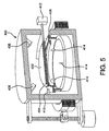
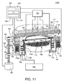
図1を次に参照して、急速熱処理チャンバ100の例示的な実施形態を示す。処理チャンバ100は、基板支持体104およびチャンバ本体102を含み、チャンバ本体102は、内部体積120を画定する壁108、底部110、および頂部または蓋112を有する。壁108は通常、基板140(図1には一部分を示す)の出し入れを容易にするために、少なくとも1つの基板アクセスポート148を含む。アクセスポートは、搬送チャンバ(図示せず)またはロードロックチャンバ(図示せず)に結合することができ、周囲の雰囲気から内部体積120を封止するスリットバルブ(図示せず)などのバルブで選択的に封止することができる。一実施形態では、基板支持体104は環状であり、チャンバ100は、基板支持体104の内径内に置かれた放射熱源106を含む。放射熱源106は通常、複数のランプを備える。変更できるRTPチャンバおよび使用できる基板支持体の例は、米国特許第6,800,833号および米国特許出願公開第2005/0191044号に記載されている。
Referring now to FIG. 1, an exemplary embodiment of a rapid
RTPチャンバ100はまた、頂部112に隣接し、頂部112に結合され、または頂部112内に形成された冷却ブロック180を含む。通常、冷却ブロック180は、放射熱源106に対向して隔置される。冷却ブロック180は、入口181Aおよび出口181Bに結合された1つまたは複数の冷媒チャネル184を備える。冷却ブロック180は、ステンレス鋼、アルミニウム、ポリマー、またはセラミック材料などのプロセスに耐える材料から作ることができる。冷媒チャネル184は、螺旋形のパターン、方形のパターン、円形のパターン、またはこれらの組合せを備えることができ、チャネル184は、たとえば冷却ブロック180を鋳造すること、および/または冷却ブロック180を2つ以上の部片から製作してこれらの部片をつなぎ合わせることによって、冷却ブロック180内に一体形成することができる。追加で、または別法として、冷却ブロック180内に穴を開けて冷媒チャネル184を形成することもできる。
The
入口181Aおよび出口181Bは、バルブおよび適切な配管によって冷媒源182に結合することができ、冷媒源182は、制御装置124と連通して、冷媒源182内に置かれる流体の圧力および/または流れの制御を容易にする。流体は、水、エチレングリコール、窒素(N2)、ヘリウム(He)、または熱交換媒体として使用される他の流体とすることができる。
図示の実施形態では、基板支持体104は任意選択で、内部体積120内で磁気的に浮上して回転するように適合される。図示の基板支持体104は、処理中に垂直に上下しながら回転することが可能であり、また処理の前、間、または後に回転しないで上下させることもできる。この磁気的浮上および/または磁気的回転により、基板支持体を上下および/または回転させるのに通常必要な動く部分の不在または低減のため、粒子の生成を防止し、または最小にする。
In the illustrated embodiment, the
チャンバ100はまた、様々な波長の熱および光に対して透過性の材料から作られた窓114を含む。この光は、赤外(IR)スペクトル内の光を含むことができ、窓114を通って、放射熱源106からの光子が基板140を加熱することができる。一実施形態では、窓114は石英材料から作られるが、サファイアなど、熱および光に対して透過性の他の材料を使用することもできる。窓114はまた、チャンバ100との間で基板の搬送を容易にするために、窓114の上部表面に結合された複数のリフトピン144を含むことができ、リフトピン144は、基板140に選択的に接触して支持するように適合される。複数のリフトピン144はそれぞれ、放射熱源106からのエネルギーの吸収を最小にするように構成され、石英材料など、窓114に使用されるものと同じ材料から作ることができる。複数のリフトピン144は、搬送ロボット(図示せず)に結合されたエンドエフェクタの通過を容易にするように位置決めし、互いから放射状に隔置することができる。別法として、エンドエフェクタおよび/またはロボットは、基板140の搬送を容易にするために、水平および垂直の動きを可能にすることもできる。
The
一実施形態では、放射熱源106は、冷媒源183に結合された冷媒アセンブリ(図示せず)内に複数のハニカムチューブ160を含む、筐体から形成されたランプアセンブリを含む。冷媒源183は、水、エチレングリコール、窒素(N2)、およびヘリウム(He)の1つまたは組合せとすることができる。筐体壁108、110は、銅材料または他の適切な材料から作ることができ、冷媒源183からの冷媒を流すのに適した冷媒チャネルが中に形成される。冷媒は、筐体が基板140より冷たくなるように、チャンバ100の筐体を冷却する。各チューブ160は、反射体と、高強度ランプアセンブリまたはIR放射器とを収容することができ、そこからハニカム状のパイプ構成が形成される。この最密な六角形のパイプ構成は、放射エネルギー源に高いパワー密度および良好な空間分解能を提供する。一実施形態では、放射熱源106は、基板を熱処理するのに、たとえば基板140上に置かれたシリコン層をアニールするのに十分な放射エネルギーを提供する。放射熱源106は、環状区域をさらに備えることができ、この環状区域内で、チューブ160からのエネルギーの放射状の分布を強化するように、制御装置124によって複数のチューブ160へ供給される電圧を変動させることができる。基板140の加熱の動的制御は、基板140全体にわたって温度を測定するように適合された1つまたは複数の温度センサ117の影響を受けることができる。
In one embodiment, the
図示の実施形態では、チャンバ本体102の壁108に任意選択のステータアセンブリ118が外接し、チャンバ本体102の外面に沿ってステータアセンブリ118の上昇を制御する1つまたは複数のアクチュエータアセンブリ122に結合される。一実施形態(図示せず)では、チャンバ100は、チャンバ本体の周りに放射状に、たとえばチャンバ本体102の周りに約120°の角度で置かれた3つのアクチュエータアセンブリ122を含む。ステータアセンブリ118は、チャンバ本体102の内部体積120内に置かれた基板支持体104に磁気的に結合される。基板支持体104は、ロータとして機能する磁気部分を備えまたは含むことができ、したがって基板支持体104を持ち上げかつ/または回転させるための磁気軸受アセンブリを作製する。一実施形態では、基板支持体104の少なくとも一部分は、流体源186に結合されたトラフ(図示せず)によって部分的に取り囲まれ、流体源186は、基板支持体に対する熱交換媒体として適合された水、エチレングリコール、窒素(N2)、ヘリウム(He)、またはこれらの組合せを含むことができる。ステータアセンブリ118はまた、ステータアセンブリ118の様々な部分および構成要素を密閉する筐体190を含むことができる。一実施形態では、ステータアセンブリ118は、懸架コイルアセンブリ170上に積み重ねた駆動コイルアセンブリ168を含む。駆動コイルアセンブリ168は、基板支持体104を回転および/または上下させるように適合され、一方懸架コイルアセンブリ170は、処理チャンバ100内で基板支持体104を受動的に中心で位置決めするように適合することができる。別法として、回転および中心位置決め機能は、単一のコイルアセンブリを有するステータによって実行することもできる。
In the illustrated embodiment, an
チャンバ本体102の内部体積120には、雰囲気制御システム164も結合される。雰囲気制御システム164は通常、チャンバ圧力を制御するスロットルバルブおよび真空ポンプを含む。雰囲気制御システム164は、内部体積120へプロセスガスまたは他の気体を提供する気体源をさらに含むことができる。雰囲気制御システム164はまた、熱蒸着プロセス、熱エッチングプロセス、およびチャンバ構成要素の現場清浄のためにプロセスガスを送達するように適合することもできる。
An
チャンバ100はまた、制御装置124を含み、制御装置124は通常、中央演算処理装置(CPU)130、支持回路128、およびメモリ126を含む。CPU130は、様々な操作を制御するために産業用の設定で使用できる任意の形式のコンピュータプロセッサおよびサブプロセッサの1つとすることができる。メモリ126またはコンピュータ可読媒体は、ランダムアクセスメモリ(RAM)、読出し専用メモリ(ROM)、フロッピーディスク、ハードディスク、またはローカルもしくは遠隔の任意の他の形式のデジタル記憶装置などの容易に利用可能なメモリの1つまたは複数とすることができ、通常、CPU130に結合される。支持回路128は、従来通り制御装置124を支持するようにCPU130に結合される。これらの回路には、キャッシュ、電源、クロック回路、入出力回路、サブシステムなどが含まれる。
The
一実施形態では、それぞれのアクチュエータアセンブリ122は通常、チャンバ本体102の壁108から延びる2つのフランジ134間に結合された高精度の親ねじ132を備える。親ねじ132は、ねじが回転するにつれて親ねじ132に沿って軸方向に進むナット158を有する。ステータ118とナット158の間には継ぎ手136が結合され、したがって親ねじ132が回転されるにつれて、継ぎ手136は、親ねじ132に沿って動き、継ぎ手136との境界面でステータ118の上昇を制御する。したがって、アクチュエータ122の1つの親ねじ132が回転して、他のアクチュエータ122のナット158間に相対的な移動をもたらすにつれて、ステータ118の水平平面は、チャンバ本体102の中心軸に対して変化する。
In one embodiment, each
一実施形態では、親ねじ132には、ステッパまたはサーボモータなどのモータ138が結合され、制御装置124による信号に応答して制御可能な回転を提供する。別法として、とりわけ空圧式シリンダ、油圧式シリンダ、ボールねじ、ソレノイド、線形アクチュエータ、およびカム従動子などの他のタイプのアクチュエータ122を利用して、ステータ118の線形位置を制御することもできる。
In one embodiment, the
任意選択のステータアセンブリ118を含む実施形態では、チャンバ100はまた、1つまたは複数のセンサ116を含むことができ、センサ116は通常、チャンバ本体102の内部体積120内の基板支持体104(または基板140)の上昇を検出するように適合される。センサ116は、チャンバ本体102および/または処理チャンバ100の他の部分に結合することができ、基板支持体104とチャンバ本体102の頂部112および/または底部110の間の距離を示す出力を提供するように適合され、また基板支持体104および/または基板140の位置合せ不良を検出することもできる。
In embodiments that include the
1つまたは複数のセンサ116は、制御装置124に結合され、制御装置124は、センサ116から出力基準値を受け取り、1つまたは複数の信号を1つまたは複数のアクチュエータアセンブリ122へ提供して基板支持体104の少なくとも一部分を上下させる。制御装置124は、センサ116から取得した位置基準値を利用して、各アクチュエータアセンブリ122のステータ118の上昇を調整することができ、したがって、RTPチャンバ100および/または放射熱源106の中心軸に対して、基板支持体104および基板支持体104上に位置する基板140の上昇と平面性の両方を調整することができる。たとえば、制御装置124は、信号を提供して1つのアクチュエータ122の操作によって基板支持体を上げ、基板支持体104の軸方向の位置合せ不良を補正することができ、または制御装置は、すべてのアクチュエータ122に信号を提供して、基板支持体104を同時に垂直に動かすのを容易にすることができる。
One or
1つまたは複数のセンサ116は、チャンバ本体102内で基板支持体104の近接を検出することが可能な超音波、レーザ、誘導性、容量性、または他のタイプのセンサとすることができる。センサ116は、頂部112近傍でチャンバ本体102に結合することができ、または壁108に結合することができるが、チャンバ100の外側のステータ118に結合するなど、チャンバ本体102内およびチャンバ本体102の周囲の他の場所も適切であろう。一実施形態では、1つまたは複数のセンサ116は、ステータ118に結合することができ、壁108を通して基板支持体104(または基板140)の上昇および/または位置を感知するように適合される。この実施形態では、壁108は、壁108を通した位置感知を容易にするために、より薄い横断面を含むことができる。
The one or
チャンバ100はまた、1つまたは複数の温度センサ117を含み、温度センサ117は、処理の前、間、および後に基板140の温度を感知するように適合することができる。図1示す実施形態では、温度センサ117は、頂部112を通って置かれるが、チャンバ本体102内およびチャンバ本体102の周囲の他の場所を使用することもできる。温度センサ117は、光高温計とすることができ、一例として、光ファイバプローブを有する高温計とすることができる。センサ117は、構成内で頂部112に結合して基板の直径全体または基板の一部分を感知するように適合することができる。センサ117は、基板の直径に実質上等しい感知領域または基板の半径に実質上等しい感知領域を画定するパターンを構成することができる。たとえば、複数のセンサ117を頂部112に放射状または線形の構成で結合して、基板の半径または直径全体にわたって感知面積を可能にすることができる。一実施形態(図示せず)では、複数のセンサ117は、頂部112のほぼ中心から頂部112の周辺部分へ放射状に延びるように1列に置くことができる。このようにして、センサ117によって基板の半径を監視することができ、これによって回転中に基板の直径の感知を可能にする。
本明細書に記載のように、チャンバ100は、基板を「上向き」に受け取るように適合され、基板の堆積物を受け取る側または面は頂部112の方へ向けられ、基板の「裏面」は放射熱源106に面している。基板の裏面は、関係する処理(すなわち、Ni被覆)に応じて基板の面より反射性が低いことがあるため、「上向き」にすることで、放射熱源106からのエネルギーを基板140によってより急速に吸収することができる。通常、パターンのない「上向き」で、より均一に吸収する面を放射源に提示する。
As described herein, the
冷却ブロック180および放射熱源106について、それぞれ内部体積120の上部部分および下部部分に位置決めされると説明しているが、冷却ブロック180および放射熱源106の位置は逆にすることができる。たとえば、冷却ブロック180は、基板支持体104の内径内に位置決めされるように寸法設定および構成することができ、放射熱源106は、頂部112に結合することができる。この構成では、石英窓114は、チャンバ100の上部部分内で放射熱源106に隣接するなど、放射熱源106と基板支持体104の間に置くことができる。基板140は、裏面が放射熱源106に面しているとき、熱をより容易に吸収でき、放射エネルギーをより均一に吸収するが、いずれの構成でも、基板140を上向きにしても下向きにしてもよい。
Although the
1つまたは複数の実施形態によれば、基板支持体104に対する基板の位置決めは、第2の基板支持体に対する基板の位置を感知する位置センサシステム220を使用して基板の位置を検出することによって、たとえば概ね平面の基板の縁部を検出することによって実現される。基板の縁部の検出は、様々な形で実現することができる。下記で論じる例は、本発明の範囲を限定しようとするものではない。他の基板位置センサシステム220も本発明の範囲内である。たとえば、特有の基板位置センサシステムは、基板支持体に対する基板の位置を検出することが可能な超音波、レーザ、誘導性、容量性、または他のタイプのセンサを利用することができる。
According to one or more embodiments, the positioning of the substrate relative to the
例示的な基板位置センサシステム220は、米国特許第7,153,185号(「’185特許」)に詳細に記載されている。基板位置検出またはセンサシステム220の一例を図2Aに示す。光源225が、光ビーム227を基板200の表面上へ誘導し、光ビーム227は、反射ビーム229として反射される。基板200から反射された光ビーム229の強度を監視するように、検出器231が位置決めされる。検出器231と基板200の一方または両方は、検出器231と基板200の間の相対的な運動を提供するように可動であることができる。センサシステム220は、検出器と通信する電子制御装置235をさらに含むことができ、制御装置235は、検出器231によって検出された反射から複数の測定値を生成するように動作可能である。
An exemplary substrate
電子制御装置235は、光センサシステムから信号を受け取る汎用のプログラム可能デジタルコンピュータを含むことができ、またはそれと通信することができる。このときこれらの測定値は、デカルトx−y座標系を使用する基板の平面で放射状の位置に関連付けることができる。
The
アルゴリズムおよび/または実験的に判定された測定値を通して、電子制御装置235は、反射が発生した基板表面上の場所を計算することができる。基板表面からの反射の性質に基づいて、制御装置は、測定値のうちどれが基板の縁部に対応するかを判定することができる。これは、基板からの反射が弱いこと、または反射がまったくないことを検出することによって判定することができる。センサシステム220は、基板より下に位置決めされて示されているが、これらの構成要素は、基板を加熱するためにランプまたは他の加熱素子によって送達される放射に干渉しないように、基板より上に位置決めできると有利であることが理解されるであろう。さらに、センサシステム220の構成要素は、高温計を含むことができる光パイプおよび温度検出システムに干渉しないように位置決めされるべきである。
Through algorithms and / or experimentally determined measurements, the
システム220の特有の実装形態は、以下の特徴の1つまたは複数を含むことができる。光ビーム227は、基板の表面上で約1ミリメートル未満のスポットサイズを有することができる。システムは、屈折光学素子(たとえば、レンズ)、反射光学素子(たとえば、鏡)、回折光学素子(たとえば、格子)、および/またはホログラフィック光学素子(たとえば、ホログラフィック格子)を含めて、ビーム集束光学系をさらに含むことができる。装置は、反射された光が検出器によって検出される前に、基板表面から反射された光を視準するように位置決めされた視準光学系をさらに含むことができる。
Specific implementations of the
図2Bに示す光検出器システムの別の実施形態では、光検出システムは、光源および検出器252を含むことができ、第2の基板支持体によって基板上に、または基板によって第2の基板支持体上に投じられる影を評価して、第2の基板支持体の位置に対する基板の位置を検出するように構成される。図2Bに示す実施形態では、検出器252は、基板支持体(縁部リング)206によって投じられる基板200上の影を検出するように位置決めされることが明らかであろう。光源250および検出器252を基板200および基板支持体206より上に位置決めして、基板200によって基板支持体206上に投じられる影を検出できることが理解される。
In another embodiment of the photodetector system shown in FIG. 2B, the photodetector system can include a light source and a detector 252 on a substrate by a second substrate support or a second substrate support by a substrate. The shadow cast on the body is evaluated and configured to detect the position of the substrate relative to the position of the second substrate support. In the embodiment shown in FIG. 2B, it will be apparent that the detector 252 is positioned to detect shadows on the
光検出システムの別の変形形態では、光源または他の適切な照射システム250は、検出器252と協働することができる。検出器252は、カメラとすることができ、視覚分析システム254と通信する。視覚分析システム254を使用して、基板支持体206および基板200の中心を検出することができる。視覚分析システム254は、実験データおよび/またはルックアップテーブルを含むことができ、また汎用コンピュータを含むことができる。
In another variation of the light detection system, a light source or other
上記のそれぞれの光学系、または基板とウェーハ支持体の相対的な位置を検出もしくは感知する任意の他の適切な方法は、基板支持体と基板の一方または両方を動かすシステムとともに使用することができる。そのようなシステムの例示的な実施形態について、以下にさらに説明する。 Each of the above optical systems or any other suitable method for detecting or sensing the relative position of the substrate and wafer support can be used with a system that moves one or both of the substrate support and the substrate. . Exemplary embodiments of such systems are further described below.
上記の位置センサシステム220の個々の構成要素は、処理チャンバの頂部または蓋112内に取り付けることができる。センサ構成要素は、ウェーハの中心位置の検出を助けるために、チャンバのXおよびY軸に沿って異なる場所に位置決めすることができる。別法として、センサシステム220の構成要素は、処理チャンバの側壁内に配置することができる。
Individual components of the
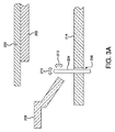
図3Aおよび3Bはまた、位置決め機構の実施形態を示す。図3Aでは、基板200は、ロードブレード202(ロボットブレード202とも呼ぶ)上でチャンバ内へロードされる。複数のリフトピン204が反射板214を貫通して突出し、基板200をロードブレードから持ち上げることができる。これは、反射板214の外周部上にリフトピンを位置決めし、ロボットブレード202の平面の面積を最小にし、したがって基板200の縁部がロボットブレード202の少なくとも一部分から張り出して、リフトピンが基板の外周縁部に接触して基板をロボットブレード202から持ち上げるようにすることによって実現することができる。したがって、ロボットブレード202は、延ばしたリフトピン204間を通って延びることができ、それによってロボットブレード202は、ピン204が基板200をロボットブレード202から持ち上げた後、後退することができる。別の変形形態では、ロボットブレード202は、基板をロボットブレードから持ち上げるリフトピンの場所と位置合せされた事前に選択された場所に、スロットまたは切込み(図示せず)を有することができる。ロボットブレードからの基板の持上げを実現する適切な方法は、米国特許第6,722,834号および第6,709,218号に見ることができる。反射板214内の孔は拡大され、それによってピンは、縁部リング206の形の基板支持体と同じX−Y平面210内で動くことができ、ならびに縁部リング206に対して直角の方向(矢印212で示す)に動くことができる。次いで、ロードブレード202をチャンバから引っ込めることができる。基板位置センサシステムは、基板200の位置を事前に選択された位置へ動かすのに必要な特定の調整を判定することができる。これは、事前に実験的に判定することができる。事前に選択された向きは、基板200がチャンバ中心に対して中心で位置決めされる向きである。これは、X−Y平面内の基板支持体206に対する基板の相対的な位置によって判定することができる。通常、基板支持体206がチャンバ中心に対して中心で位置決めされる場合、基板200および基板支持体206が中心で位置決めされた向きであるとき、基板200はチャンバ内で中心で位置決めされるはずである。次いで、リフトピン204は、基板200が縁部リング206と同軸になるまで、反射板214内の拡大した孔208内で動くことができる。基板200が所望の位置にきた後、図3Bに示すように、リフトピン204は後退して、基板200を縁部リング206へ下げることができる。縁部リング206内に孔を開けたり、彫ったりすることが望ましいが、リフトピン204は縁部リング206に交差しないため、必ずしも必要ではない。
3A and 3B also show an embodiment of a positioning mechanism. In FIG. 3A, the
別法として、リフトピン204は、反射板214内に固定することができる。次いで反射板は、縁部リング206と同じ平面210内で動かすことができ、ならびに縁部リング206に対して直角212に動かすことができる。それによって、基板200を縁部リング206上に位置決めすることができる。
Alternatively, the lift pins 204 can be fixed in the
図3Cは、縁部リング206および反射板214の横断面図を示す。反射板214内の孔208は、リフトピン204の直径より大きいことがわかる。これにより、リフトピン204は、3次元に動いて基板の位置を調整することができる。
FIG. 3C shows a cross-sectional view of the
図4は、位置決め機構を利用するチャンバの例示的な実施形態を示す。基板302は、開口320を通ってロードブレード318上でチャンバ300内へロードされ、基板302を支持するロードブレード318は、下記のように最適の位置が得られるまで、チャンバ内に留まる。基板位置センサシステム304(たとえば、上記のタイプ)は、第2の基板支持体306に対する基板302の位置に調整が必要かどうかを判定することができる。第2の基板支持体306は、基板302の縁部で基板を支持する縁部リングとして示す。次いで、基板位置センサシステム304および位置決め機構と通信するコンピュータまたは他の適切なプロセッサを使用して、基板支持体306に対する基板302の位置を調整することができる。縁部リング306に対する調整は、縁部リング306を所望の放射状の方向に押しまたは動かすプッシャ310を含む放射状の位置決め機構を使用して、方向性の力をかけることによって行うことができる。別法として、プッシャ310は、磁気的に浮上しているロータ308に方向性の力をかけて基板支持体306を所望の方向に動かすことができる。基板支持体306が基板302と同軸に位置決めされた後、リフトピン312は、基板302をロードブレードから持ち上げる。ロードブレードが取り除かれた後、リフトピン312は、基板302を基板支持体306へ下げることができ、その結果、基板支持体306と基板302を同軸に位置合せする。
FIG. 4 illustrates an exemplary embodiment of a chamber that utilizes a positioning mechanism. The
方向性の力をかけることによって縁部リングまたは磁気的に浮上させたロータを動かすことは、様々な他の形で実現することもできる。放射状の位置決め機構の非限定的な例には、一連の位置決め棒310で縁部リング306もしくはロータ308を押すこと、気体または液体を噴射して縁部リングもしくはロータを押すこと、またはステータを使用して磁界を印加し、縁部リング306もしくはロータ308を動かすことが含まれる。ねじ式、油圧式、または空圧式のプッシャ機構など、任意の適切なプッシャ機構を使用して、位置決め棒310を駆動させることができる。
Moving the edge ring or magnetically levitated rotor by applying a directional force can also be realized in a variety of other ways. Non-limiting examples of radial positioning mechanisms include pushing the
別の実施形態では、図5に示すように、基板402は、ロードブレード404上でチャンバ400内へロードされる。基板位置センサシステム406(たとえば、上記のタイプ)が、基板402と縁部リング408を同軸に位置させるのに必要な調整を判定することができる。ロードブレード404は、基板402を位置決めするように、プロセッサまたはコンピュータを介して基板位置センサシステム406と通信する押す機構410またはモータ412によって動かすことができる。リフトピン414が、基板402をロードブレード404から持ち上げる。ロードブレード404を取り出すと、リフトピン414は下がり、それによって基板402を縁部リング408上へ同軸の関係になるように配することができる。
In another embodiment, the
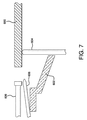
図6に示すさらなる実施形態では、基板502は、ロードブレード504上でチャンバ500内へ運ばれる。上記のタイプの基板位置センサシステム506が、基板502と縁部リング508を同軸の関係になるように配置するのに必要な調整を判定する。基板位置センサシステムは、プロセッサまたはコンピュータおよび位置決め機構と通信する。次いで、基板502は、ロードブレード504上に位置したまま、モータ駆動式位置決め棒、油圧式もしくは空圧式位置決め棒、液体もしくは気体噴射、または他の類似の手段510の1つまたは複数から選択された位置決め機構を使用して定位置へ押される。これらの位置決め機構は、ブレード自体の上に位置することもできる。位置合せした後、リフトピン512は、基板502をロードブレード504から持ち上げる。ロードブレード504は後退し、リフトピン512は基板502を縁部リング508上へ同軸の関係になるように下げる。
In a further embodiment shown in FIG. 6, the
図7に示す別の実施形態では、基板600は、リフトピン604上に位置したまま、縁部リング602と同軸に位置合せすることができる。これらの実施形態では、基板600は、それだけに限定されるものではないが、モータ駆動式位置決め棒606、油圧もしくは空圧駆動式位置決め棒、および/またはノズル608を通した気体もしくは液体の噴射からの圧力を含めて、任意の適切な手段によって側面から押すことができる。位置合せした後、リフトピン604は後退し、基板600を縁部リング602へ、同軸に位置合せされた関係になるように下げる。
In another embodiment shown in FIG. 7, the
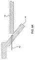
図8Aおよび8Bに示すさらなる実施形態では、基板700を縁部リング702上に配置した後、縁部リング702との基板700の同軸の位置合せを可能にする。この位置合せは、それだけに限定されるものではないが、モータ駆動式位置決め棒704、油圧もしくは空圧駆動式位置決め棒、またはノズル706を通した気体もしくは液体の噴射からの圧力を含めて、任意の適切な手段によって実現することができる。縁部リング702と同軸に位置合せされると、基板700は、処理する準備ができる。
In a further embodiment shown in FIGS. 8A and 8B, after placing the
1つまたは複数の詳細な実施形態の装置は、約±0.005インチの範囲内で同軸になるように縁部リングと基板を正確かつ再現可能に位置決めすることが可能である。より詳細な実施形態では、基板と縁部リングは、約±0.002インチの範囲内または約±0.001インチの範囲内で同軸になるように位置決めされる。 The device of one or more detailed embodiments is capable of accurately and reproducibly positioning the edge ring and the substrate to be coaxial within a range of about ± 0.005 inches. In more detailed embodiments, the substrate and edge ring are positioned to be coaxial within a range of about ± 0.002 inches or within a range of about ± 0.001 inches.
したがって、本発明の1つまたは複数の実施形態は、基板を処理する急速熱処理装置を対象とする。この装置は、熱源を含むチャンバを備える。装置は、チャンバ内の基板を第1の位置で保持する、通常リフトピンまたはロボットブレードの形の第1の基板支持体と、基板を第2の位置で保持する第2の基板支持体、たとえば縁部リングとを含む。第2の基板支持体は、特有の実施形態では基板をその縁部で支持する縁部リングを構成し、熱処理中に基板を保持するように適合されており、基板を熱源へ近づけたり遠ざけたりする方向に可動である。基板の軸方向の位置を感知するセンサシステムが含まれる。センサシステムは、第2の基板支持体の軸方向の位置に対する基板の軸方向の位置を変化させるように動作するアクチュエータと通信する。第1の基板支持体は、一時的な基板支持体として働くことができ、そのように呼ぶ。 Accordingly, one or more embodiments of the present invention are directed to a rapid thermal processing apparatus for processing a substrate. This apparatus comprises a chamber containing a heat source. The apparatus includes a first substrate support, typically in the form of lift pins or robot blades, that holds the substrate in the chamber in a first position, and a second substrate support, eg, an edge, that holds the substrate in a second position. Part ring. The second substrate support, in a particular embodiment, constitutes an edge ring that supports the substrate at its edge and is adapted to hold the substrate during heat treatment, moving the substrate closer to or away from the heat source. It is movable in the direction of A sensor system for sensing the axial position of the substrate is included. The sensor system communicates with an actuator that operates to change the axial position of the substrate relative to the axial position of the second substrate support. The first substrate support can act as a temporary substrate support and is referred to as such.
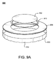
図9Aは、基板支持体900の一実施形態の上面図である。図9Bは、基板支持体900の横断面図である。基板支持体900は、縁部リング910、支持リング920、および支持シリンダ930を含む複数の部分のアセンブリから形成される。縁部リング910は、基板902の配置を容易にする環状の形状を有する。図9Bに示すように、縁部リング910は、外側表面912と、外側表面912に対して平行であり、外側表面912からくぼんだ内側表面914とを含む。それによって外側表面912は、内側表面914より高いレベルに位置し、内側表面914は、側壁915によって区切られた外縁を有する。側壁915は、基板902の厚さよりわずかに高くして、内側表面914上に基板902を配置するのを容易にすることができる。縁部リング910はまた、外側表面912から下方へ延びる外側フランジ916を含むことができる。外側フランジ916と側壁915の間には間隙918が画定され、縁部リング910を支持リング920上に組み立てるのを容易にする。一実施形態では、縁部リング910は、容易な取外しおよび交換のための付属物がなくても、支持リング920上に簡単に置くことができる。詳細な実施形態では、第2の基板支持体は、薄い固体の凹状の円板とすることができる。
FIG. 9A is a top view of one embodiment of a
支持リング920は薄い平坦な区間を含み、内側フランジ922が上方へ延び、外側フランジ924が下方へ延びる。上方へ延びる内側フランジ922は、縁部リング910の外側フランジ916に結合される。下方へ延びる外側フランジ924は、支持シリンダ930に結合される。支持シリンダ930は、支持リング920に垂直方向の支持を提供する。図9Aに示すように、支持シリンダ930の底部932は、支持シリンダ930内への空気の流れを可能にするジグザグ形のプロファイルを含むことができる。
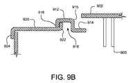
縁部リング910の代替実施形態を図9Cに示す。この実施形態では、内側表面914はまた、基板902上に提供された対応する位置合せマーク904の位置合せを容易にするための参照として使用できる位置合せマーク919を含むことができる。一実施形態では、内側表面914上の位置合せマーク919は突起として形成することができ、基板902の縁上の位置合せマーク904はノッチとすることができる。縁部リング910上の基板902の正しい位置合せおよび向きによって、光の漏れによる均一でない熱分布を防止し、熱伝達を改善することができる。
An alternative embodiment of the
図10Aの上面図および図10Bの側面図に示すように、位置センサ1014および1016を使用して、処理チャンバ1001内で基板1002が基板支持体1004の縁部リング1003に対して正しく中心で位置決めされるようにすることもできる。一実施形態では、位置センサ1014および1016は、たとえば位置センサ1014および1016をチャンバの蓋の近傍に取り付けることによって、基板支持体1004より上に配置することができる。位置センサ1014および1016は、基板1002の縁部1006と縁部リング1003の側壁1005の間の距離を検出することが可能な超音波センサ、光センサ、誘導性センサ、容量性センサ、または他のタイプの位置センサを含むことができる。別の実施形態では、位置センサ1014および1016は、光ビームを放出して、縁部リング1003に対する基板1002のあらゆる不適正な中心の位置決めを検出することができる。
As shown in the top view of FIG. 10A and the side view of FIG. 10B,
図10Bに示すように、基板1002は、支持ピン1007を下げることによって縁部リング1003上に配置することができる。基板1002に基板表面全体にわたって均一の熱処置を供給するために、基板1002を縁部リング1003の中心上に位置決めすることができる。縁部リング1003は、基板支持体1004をX軸およびY軸の方向に動かすことによって、基板1002に接するように調整することができる。基板1002を位置決めするための縁部リング1003の中心位置を見つけるためには、中心位置の検出を助けるように、位置センサ1014および1016を異なる場所に位置決めすることができる。一実施形態では、位置センサ1014は、図10Bに示すように、基板1002の縁部1006と縁部リング1003の側壁1005の間のスポットに対して、チャンバの蓋1015上に取り付けることができる。各スポットには、基板1002の縁部1006と縁部リング1003の側壁1005の間の距離1008が存在する。各スポットは、軸、および特有の軸に対する距離に対応することができる。たとえば、位置センサ1014に対するスポットはX軸に対応することができ、位置センサ1016に対するスポットはY軸に対応することができる。各スポットは、位置センサ1014および1016によって測定できる距離1008を包含することができる。一実施形態では、位置センサ1014および1016は、光ビーム1011を放出して、スポット内の距離1008を検出することができる。別の実施形態では、反射する光ビーム1011は、円形のスポットまたは線とすることができる。さらに別の実施形態では、円形のスポットのスポットサイズまたは線は、4.5mm以上とすることができる。さらに別の実施形態では、反射する光ビーム1011は、約25〜50mmの範囲内で伝送することができる。各スポットで測定される距離1008を比較して、シータ調整値を見出すことができる。一実施形態では、測定される距離に対する精度は、約±10μm以上の範囲を有することができる。シータ調整値は、X軸に対する調整可能な距離およびY軸に対する調整可能な距離を包含する。これらの調整可能な距離は、縁部リング1003をX軸およびY軸の中心位置内へ動かすのに必要な調整である。シータ調整値を取得した後、正しい位置へ動くように縁部リング1003を調整することができる。次いで、ロボットアームへ信号を送って支持ピン1007から基板1002を持ち上げ、熱処置のために基板1002を基板支持体1004上の正しい位置へ搬送することができる。一実施形態では、基板から縁部リングへの距離は約0〜4.342mmの範囲である。特有の実施形態では、基板から縁部リングへの距離は約2.171mmである。詳細な実施形態では、シータ調整値は、垂直に動かすことによって調整できるZ位置に関する調整情報に関連する。
As shown in FIG. 10B, the
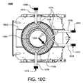
図10Cは、本発明の別の実施形態による処理チャンバ1050内の基板支持体1052の上面図である。別法として、縁部リング1056と基板1054の間の距離1008はまた、処理チャンバ1050の内側側壁にセンサを配置することによって測定することもできる。一実施形態では、内側側壁の片側には、第1の光伝送器1068を結合することができ、第1の光伝送器1068がX軸に対応する距離1058を測定するように位置決めされる場合、その側壁に隣接する側壁に第1の光受信器1070を結合することができる。別の内側側壁には、第2の光伝送器1072を結合することができ、第2の光伝送器1072がY軸に対応する距離1059を測定するように位置決めされる場合、その内側側壁に隣接する側壁に第2の光受信器1074を結合することができる。距離1058および1059は、光伝送器1068および1072によって光パイプ1078を通って伝送される光ビーム1076によって測定することができる。光ビーム1076は、縁部リング1056と基板1054の間で距離1058および1059を通過することができ、光受信器1070および1074によって受け取ることができる。距離1058および1059を取得してシステム制御装置1124へ送り返した後、シータ調整値を計算することができ、次いで縁部リング1003は、基板を位置決めできる中心の位置へX軸およびY軸の方向に動くことによって、シータ調整値に従って調整することができる。
FIG. 10C is a top view of the
図11は、急速熱処理チャンバ1100の詳細な実施形態の簡略化した等角図を示す。処理チャンバ1100は、図1に関して記載の構成要素を含み、同等の構成要素に対する参照番号は変わらない。チャンバ1100は、1つまたは複数のセンサ116を含み、センサ116は通常、チャンバの外側に位置しており、チャンバ本体102の内部体積120内の基板支持体104(または基板140)の上昇を検出するように適合される。センサ116は、図示の管状のポートおよび/または処理チャンバ1100の他の部分を通ってチャンバ本体102に結合することができ、基板支持体104とチャンバ本体102の頂部112および/または底部110の間の距離を示す出力を提供するように適合され、また基板支持体104および/または基板140の位置合せ不良を検出することもできる。別の実施形態(図示せず)では、センサ116は、ステータ筐体1190内部に配置することができ、それによってセンサ116は、ステータ118とともに上下に動くことができるはずである。この実施形態により、センサ116は、リング区間1192上の基準点を取得することができるはずである。そのような実施形態では、信号は、一定である可能性が高く、信号の偏差を探すはずであり、モータ138からのフィードバックから垂直方向の位置を判定することができる。
FIG. 11 shows a simplified isometric view of a detailed embodiment of the rapid
1つまたは複数のセンサ116は、制御装置124に結合され、制御装置124は、センサ116から出力基準値を受け取り、1つまたは複数の信号を1つまたは複数のアクチュエータアセンブリ122へ提供して基板支持体104を上下させる。制御装置124は、センサ116から取得した位置基準値を利用して、各アクチュエータアセンブリ122のステータ118の上昇を調整することができ、したがって、チャンバ100および/または放射熱源106の中心軸に対して、基板支持体104および基板支持体上に位置する基板140の上昇と平面性の両方を調整することができる。たとえば、制御装置124は、信号を提供してアクチュエータ122の操作によって基板支持体を上げ、基板支持体104の軸方向の位置合せ不良を補正することができ、または制御装置は、すべてのアクチュエータ122に信号を提供して、基板支持体104を同時に垂直に動かすのを容易にすることができる。
One or
センサ116は、壁108に結合することができるが、チャンバ1100の外側のステータ118に結合するなど、チャンバ本体102内およびチャンバ本体102の周囲の他の場所も適切であろう。一実施形態では、1つまたは複数のセンサ116は、ステータ118に結合することができ、壁108を通して基板支持体104(または基板140)の上昇および/または位置を感知するように適合される。これらの実施形態では、壁108は、壁108を通した位置感知を容易にするために、より薄い横断面を含むことができる。
The
図11の基板支持体104は、放射熱源106および他のハードウェア(図示せず)を受け取るように寸法設定された内径を有する環状の本体1191を含む。基板支持体104は、少なくとも部分的に、磁気リング区間1192および支持区間1194からなる。磁気リング区間1192は、基板支持体104とステータ118の磁気結合を容易にするために、少なくとも部分的に、鉄含有材料などの磁気材料からなることができる。鉄含有材料には低炭素鋼、ステンレス鋼が含まれ、これにはニッケルなどのめっきを含むことができる。一実施形態では、磁気リング区間1192は、中心軸の周りに極性配列で置かれた複数の永久磁石からなる。磁気リング区間1192は、1つまたは複数のチャネルが形成された外側表面をさらに含むことができる。一実施形態では、磁気リング区間1192は、1つまたは複数のチャネルが形成された「E」字状または「C」字状などの成形プロファイルを含む。
The
1つまたは複数の実施形態によれば、基板140を持ち上げる前に、リフトピン144上の基板140と同軸になるように磁気的に浮上させた基板支持体104の位置を調整することによって、縁部リング104上で基板140を中心で位置決めすることが可能である。システム制御装置124と通信する1組の光センサ116または視覚システムを含むフィードバックシステムを使用して、基板の中心の位置決めを実現することができる。基板140の配置は、そのようなシステムからのフィードバックを使用して行うことができる。ステータ118は、たとえば0.001”以上の高い精度で、縁部リング104を基板140より下に中心で位置決めするために使用することができ、最高0.010”の移動を補償することができる。
According to one or more embodiments, the edge is adjusted by adjusting the position of the
本発明の1つまたは複数の実施形態は、基板140をチャンバ1100内へ運ぶロボット(図示せず)を有し、基板140はリフトピン144上へ搬送される。基板支持体104は、ステータ118によって生成される可変の磁界を使用して、基板140より下に中心で位置決めされる。ステータ118は、チャンバ内で基板支持体104の位置を変化させる。図12は、筐体が取り外されたステータアセンブリ118の一実施形態の上面図を示す。システム制御装置と通信する一連の電磁石1200の磁界強度は、電磁バイアスを生じさせるように調整することができ、それによってチャンバ内で基板支持体を押したり引いたりすることができる。少なくとも1つの電磁石にバイアスをかけて基板支持体を押すことができ、また少なくとも1つの電磁石にバイアスをかけて基板支持体を引くことができる。ステータ118の周りの様々な場所に位置する電磁石1200の磁界の強度を調整することによって、基板支持体を正確に位置決めすることができる。システム制御装置124と通信するセンサ1202を用いて、チャンバ内の基板支持体の位置を検出することができ、それによって位置信号の形でフィードバックをシステム制御装置124に提供することができる。センサ1202は、渦電流センサとすることができる。これらのセンサ1202からのフィードバックは、システム制御装置124によって評価することができ、システム制御装置124は、信号を提供して電磁石の1つまたは複数にバイアスをかけ、基板支持体の位置を調整することができる。
One or more embodiments of the present invention include a robot (not shown) that carries the
図12は、約120°離れた位置に位置する電磁石1200およびセンサ1202を示す。これは例示のみを目的とし、本発明を限定すると見なすべきではない。任意の適切な数のセンサおよび電磁石を用いることができる。たとえば、システム制御装置124によって6つの電磁石を制御することができ、フィードバックは3つのセンサから発生する。
FIG. 12 shows
本発明のさらなる実施形態は、基板を処理する方法を対象とする。この方法は、基板を処理チャンバ内へ搬送するステップを含む。基板は、中間基板支持体へ搬送される。中間基板支持体は、たとえば1組のリフトピンとすることができる。基板の場所は、たとえば1つまたは複数の基板縁部を検出することによって判定される。基板支持体に対する基板の位置は、基板および基板支持体が事前に選択された相対的な向きで位置合せされるように調整される。基板位置センサシステムは、中央演算処理装置、たとえば汎用コンピュータを通して位置決め機構と通信し、位置決め機構は、基板支持体に対する基板の位置に所望の調整を加える。フィードバック制御システムを使用して、基板と基板支持体が実質的に同軸に位置合せされるまで、基板と基板支持体の相対的な位置を最適化することができる。基板は、第2の基板支持体へ搬送される。第2の基板支持体は、縁部リングとすることができる。それで基板は、処理する準備ができる。規定の相対的な向きは、基板と縁部リングの軸方向の位置合せ、または実験的に判定された位置に基づく基板と縁部リングの位置合せとすることができる。たとえば、実験的に判定された位置では、基板と縁部リングを同軸に位置合せしないことがあるが、基板の質量の熱中心と縁部リングの中心を位置合せすることができる。 A further embodiment of the invention is directed to a method of processing a substrate. The method includes transporting a substrate into the processing chamber. The substrate is transferred to an intermediate substrate support. The intermediate substrate support can be, for example, a set of lift pins. The location of the substrate is determined, for example, by detecting one or more substrate edges. The position of the substrate relative to the substrate support is adjusted so that the substrate and the substrate support are aligned in a preselected relative orientation. The substrate position sensor system communicates with the positioning mechanism through a central processing unit, such as a general purpose computer, which makes the desired adjustment to the position of the substrate relative to the substrate support. A feedback control system can be used to optimize the relative position of the substrate and substrate support until the substrate and substrate support are aligned substantially coaxially. The substrate is transported to the second substrate support. The second substrate support can be an edge ring. The substrate is then ready for processing. The defined relative orientation may be an axial alignment of the substrate and edge ring, or an alignment of the substrate and edge ring based on an experimentally determined position. For example, at experimentally determined positions, the substrate and edge ring may not be aligned coaxially, but the thermal center of the substrate mass and the center of the edge ring can be aligned.
基板は、ロボットブレードを使用して処理チャンバ内へ搬送することができる。中間支持体は、リフトピンアセンブリ上に位置する複数のリフトピンとすることができる。チャンバへの基板の導入および中間支持体の提供の他の方法も、本発明の範囲内である。 The substrate can be transferred into the processing chamber using a robot blade. The intermediate support can be a plurality of lift pins located on the lift pin assembly. Other methods of introducing a substrate into the chamber and providing an intermediate support are also within the scope of the present invention.
これらのステップの順序は、使用する特定の実施形態に応じて変動し、厳密な手続き上のシーケンスと見なすべきではない。いくつかの実施形態では、縁部リングに対する基板の相対的な位置は、基板をリフトピン上へ搬送する前に調整される。他の実施形態では、縁部リングに対する相対的な位置は、基板をリフトピンへ搬送した後に調整される。様々な実施形態では、縁部リングに対する基板の相対的な位置は、基板の場所、縁部リングの場所、またはリフトピンの場所の1つまたは複数を変化させることによって調整される。 The order of these steps will vary depending on the particular embodiment used and should not be considered a strict procedural sequence. In some embodiments, the relative position of the substrate relative to the edge ring is adjusted prior to transporting the substrate onto the lift pins. In other embodiments, the relative position to the edge ring is adjusted after transporting the substrate to the lift pins. In various embodiments, the relative position of the substrate relative to the edge ring is adjusted by changing one or more of the substrate location, the edge ring location, or the lift pin location.
詳細な実施形態は、浮上している基板支持体上に基板を同心円状に位置決めする方法を対象とする。基板が処理チャンバ内へ搬送され、一時的な支持要素上へ配置される。基板支持体に対する基板の位置は、センサを使用して測定される。基板支持体の位置は、基板支持体と基板を同心円状に位置合せするように調整される。基板は、一時的な支持要素から基板支持体へ搬送される。 Detailed embodiments are directed to a method of concentrically positioning a substrate on a floating substrate support. The substrate is transferred into the processing chamber and placed on a temporary support element. The position of the substrate relative to the substrate support is measured using a sensor. The position of the substrate support is adjusted so that the substrate support and the substrate are aligned concentrically. The substrate is transported from the temporary support element to the substrate support.
特有の実施形態では、支持体上の基板の同心円状の位置決めは、少なくとも1つの磁石にバイアスをかけて基板支持体を押したり引いたりするステップを含む。 In a specific embodiment, concentric positioning of the substrate on the support includes biasing at least one magnet to push or pull the substrate support.
さらなる特有の実施形態は、チャンバ、基板支持体、位置センサ、およびシステム制御装置を備える基板処理装置を対象とする。基板支持体は、チャンバ内に置かれ、上部表面上に基板を支持するように構成された環状の本体を備える。基板支持体は、基板支持体に隣接して置かれた複数の電磁石に磁気的に結合される。位置センサは、基板支持体に対する基板の位置を検出することができる。システム制御装置は、電磁石と通信し、電磁石の少なくとも1つにバイアスをかけて基板に対して基板支持体を動かす(すなわち、押したり引いたりする)ように動作する。 A further specific embodiment is directed to a substrate processing apparatus comprising a chamber, a substrate support, a position sensor, and a system controller. The substrate support comprises an annular body placed in the chamber and configured to support the substrate on the upper surface. The substrate support is magnetically coupled to a plurality of electromagnets placed adjacent to the substrate support. The position sensor can detect the position of the substrate relative to the substrate support. The system controller communicates with the electromagnet and operates to bias (i.e. push and pull) the substrate support relative to the substrate by biasing at least one of the electromagnets.
この明細書全体にわたって、「一実施形態(one embodiment)」、「特定の実施形態」、「1つまたは複数の実施形態」、または「一実施形態(an embodiment)」に対する言及は、その実施形態に関連して記載の特定の特徴、構造、材料、または特性が、本発明の少なくとも1つの実施形態に含まれることを意味する。したがって、この明細書全体にわたって様々な箇所に「1つまたは複数の実施形態で」、「特定の実施形態で」、「一実施形態(one embodiment)で」、または「一実施形態(an embodiment)で」などの語句が見られることは、必ずしも本発明の同じ実施形態に言及しているというわけではない。さらに、1つまたは複数の実施形態では、特定の特徴、構造、材料、または特性を、任意の適切な形で組み合わせることができる。 Throughout this specification, references to “one embodiment”, “a particular embodiment”, “one or more embodiments”, or “an embodiment” refer to that embodiment. Any particular feature, structure, material, or characteristic described in connection with is meant to be included in at least one embodiment of the invention. Accordingly, in various places throughout this specification, “in one or more embodiments”, “in a particular embodiment”, “in one embodiment”, or “an embodiment”. The appearance of phrases such as “in” does not necessarily refer to the same embodiment of the invention. Further, in one or more embodiments, particular features, structures, materials, or characteristics may be combined in any suitable manner.
本明細書では本発明について、特定の実施形態を参照して説明したが、これらの実施形態は、本発明の原理および応用例を例示するものにすぎないことを理解されたい。本発明の精神および範囲から逸脱することなく、本発明の方法および装置に様々な修正および変形を加えることができることが、当業者には明らかであろう。したがって、本発明は、添付の特許請求の範囲およびその均等物の範囲内にある修正形態および変形形態を含むものとする。 Although the invention herein has been described with reference to particular embodiments, it is to be understood that these embodiments are merely illustrative of the principles and applications of the present invention. It will be apparent to those skilled in the art that various modifications and variations can be made to the method and apparatus of the present invention without departing from the spirit and scope of the invention. Thus, it is intended that the present invention include modifications and variations that are within the scope of the appended claims and their equivalents.
Claims (5)
熱源を含むチャンバと、
前記チャンバ内の前記基板を第1の位置で保持する第1の基板支持体と、
熱処理中に前記基板を保持し、前記基板を前記熱源へ近づけたり遠ざけたりする方向に可動である、第2の位置の第2の基板支持体と、
前記第2の基板支持体に対する前記基板の位置を感知し、アクチュエータと通信して前記第2の基板支持体の軸方向の中心を前記基板の中心に位置決めするように、前記第2の基板支持体を動かすセンサとを備え、
前記センサが、前記第2の基板支持体によって前記基板上に、または前記基板によって前記第2の基板支持体上に投じられる影を評価して、前記第2の基板支持体の位置に対する前記基板の位置を検出する装置。 A rapid thermal processing apparatus for processing a planar substrate,
A chamber containing a heat source;
A first substrate support for holding the substrate in the chamber in a first position;
A second substrate support in a second position that holds the substrate during a heat treatment and is movable in a direction to move the substrate closer to or away from the heat source;
Sensing the position of the substrate relative to the second substrate support and communicating with an actuator to position the axial center of the second substrate support at the center of the substrate. A sensor that moves the body,
The sensor evaluates a shadow cast on the substrate by the second substrate support or on the second substrate support by the substrate, and the substrate relative to the position of the second substrate support A device that detects the position of the machine.
Applications Claiming Priority (7)
| Application Number | Priority Date | Filing Date | Title |
|---|---|---|---|
| US11200808P | 2008-11-06 | 2008-11-06 | |
| US11201508P | 2008-11-06 | 2008-11-06 | |
| US61/112,008 | 2008-11-06 | ||
| US61/112,015 | 2008-11-06 | ||
| US12/611,958 US8314371B2 (en) | 2008-11-06 | 2009-11-04 | Rapid thermal processing chamber with micro-positioning system |
| US12/611,958 | 2009-11-04 | ||
| PCT/US2009/063394 WO2010054076A2 (en) | 2008-11-06 | 2009-11-05 | Rapid thermal processing chamber with micro-positioning system |
Publications (3)
| Publication Number | Publication Date |
|---|---|
| JP2012508456A JP2012508456A (en) | 2012-04-05 |
| JP2012508456A5 JP2012508456A5 (en) | 2012-12-20 |
| JP6079980B2 true JP6079980B2 (en) | 2017-02-15 |
Family
ID=42153545
Family Applications (1)
| Application Number | Title | Priority Date | Filing Date |
|---|---|---|---|
| JP2011534920A Active JP6079980B2 (en) | 2008-11-06 | 2009-11-05 | Rapid thermal processing chamber with micropositioning system |
Country Status (6)
| Country | Link |
|---|---|
| US (4) | US8314371B2 (en) |
| JP (1) | JP6079980B2 (en) |
| KR (3) | KR101831360B1 (en) |
| CN (1) | CN102210017B (en) |
| DE (1) | DE112009002691T5 (en) |
| WO (1) | WO2010054076A2 (en) |
Families Citing this family (51)
| Publication number | Priority date | Publication date | Assignee | Title |
|---|---|---|---|---|
| US8314371B2 (en) * | 2008-11-06 | 2012-11-20 | Applied Materials, Inc. | Rapid thermal processing chamber with micro-positioning system |
| US8109669B2 (en) * | 2008-11-19 | 2012-02-07 | Applied Materials, Inc. | Temperature uniformity measurement during thermal processing |
| US9282592B2 (en) | 2009-02-27 | 2016-03-08 | Taiwan Semiconductor Manufacturing Company, Ltd. | Rotatable heating-cooling plate and element in proximity thereto |
| DE102011007682A1 (en) * | 2011-04-19 | 2012-10-25 | Siltronic Ag | Susceptor for supporting a semiconductor wafer and method for depositing a layer on a front side of a semiconductor wafer |
| US8649017B2 (en) * | 2011-08-16 | 2014-02-11 | Applied Materials, Inc. | Methods and apparatus for sensing a substrate in a chamber |
| JP5676398B2 (en) * | 2011-08-29 | 2015-02-25 | 株式会社Sebacs | Substrate temperature measurement system |
| US9548223B2 (en) | 2011-12-23 | 2017-01-17 | Lam Research Ag | Apparatus for treating surfaces of wafer-shaped articles |
| KR101829676B1 (en) * | 2011-12-29 | 2018-02-20 | 삼성전자주식회사 | Method of thermally treating wafer |
| US9330949B2 (en) * | 2012-03-27 | 2016-05-03 | SCREEN Holdings Co., Ltd. | Heat treatment apparatus for heating substrate by irradiating substrate with flash of light |
| US9960059B2 (en) * | 2012-03-30 | 2018-05-01 | Taiwan Semiconductor Manufacturing Company, Ltd. | Honeycomb heaters for integrated circuit manufacturing |
| KR101418555B1 (en) * | 2012-08-06 | 2014-07-15 | 인하대학교 산학협력단 | Chamber for an aerodynamic levitator |
| EP2923376A4 (en) * | 2012-11-21 | 2016-06-22 | Ev Group Inc | Accommodating device for accommodation and mounting of a wafer |
| KR102271250B1 (en) * | 2013-05-15 | 2021-06-30 | 어플라이드 머티어리얼스, 인코포레이티드 | Diffuser for lamp heating assembly |
| JP6114668B2 (en) * | 2013-09-18 | 2017-04-12 | 東京エレクトロン株式会社 | Substrate processing apparatus and substrate processing method |
| CN104655880A (en) * | 2013-11-19 | 2015-05-27 | 鸿富锦精密电子(天津)有限公司 | Testing turntable |
| US9929029B2 (en) * | 2015-10-15 | 2018-03-27 | Applied Materials, Inc. | Substrate carrier system |
| JP2017184198A (en) | 2016-03-31 | 2017-10-05 | ソニー株式会社 | Image sensor, imaging device, image sensor identification method, image forgery prevention method and image alteration restriction method |
| US9892956B1 (en) * | 2016-10-12 | 2018-02-13 | Lam Research Corporation | Wafer positioning pedestal for semiconductor processing |
| US10573549B2 (en) | 2016-12-01 | 2020-02-25 | Lam Research Corporation | Pad raising mechanism in wafer positioning pedestal for semiconductor processing |
| US9960068B1 (en) | 2016-12-02 | 2018-05-01 | Lam Research Corporation | Moment cancelling pad raising mechanism in wafer positioning pedestal for semiconductor processing |
| TWI766897B (en) * | 2016-11-09 | 2022-06-11 | 美商東京威力科創Fsi股份有限公司 | An apparatus for treating a microelectronic substrate and method thereof |
| NL2017773B1 (en) * | 2016-11-11 | 2018-05-24 | Suss Microtec Lithography Gmbh | Positioning device |
| TWI765936B (en) | 2016-11-29 | 2022-06-01 | 美商東京威力科創Fsi股份有限公司 | Translating and rotating chuck for processing microelectronic substrates in a process chamber |
| TWI760394B (en) | 2016-12-07 | 2022-04-11 | 美商東京威力科創Fsi股份有限公司 | Wafer edge lift pin design for manufacturing a semiconductor device |
| US9964863B1 (en) * | 2016-12-20 | 2018-05-08 | Applied Materials, Inc. | Post exposure processing apparatus |
| US10655224B2 (en) * | 2016-12-20 | 2020-05-19 | Lam Research Corporation | Conical wafer centering and holding device for semiconductor processing |
| WO2018140789A1 (en) | 2017-01-27 | 2018-08-02 | Tel Fsi, Inc. | Systems and methods for rotating and translating a substrate in a process chamber |
| KR101948522B1 (en) | 2017-06-05 | 2019-04-29 | 홍승환 | Wafer Magazine of Which Size Can be Adjusted |
| JP6948860B2 (en) * | 2017-07-14 | 2021-10-13 | 株式会社荏原製作所 | Board holding device |
| CN109686677A (en) * | 2017-10-19 | 2019-04-26 | 德淮半导体有限公司 | A kind of semiconductor processing equipment |
| JP2019079867A (en) * | 2017-10-20 | 2019-05-23 | 漢民科技股▲分▼有限公司 | Gaseous phase deposition device |
| KR20200121829A (en) | 2018-02-19 | 2020-10-26 | 티이엘 매뉴팩처링 앤드 엔지니어링 오브 아메리카, 인크. | Microelectronic treatment system with treatment spray with controllable beam size |
| US11594445B2 (en) | 2018-03-13 | 2023-02-28 | Applied Materials, Inc. | Support ring with plasma spray coating |
| KR102433436B1 (en) | 2018-07-04 | 2022-08-17 | 삼성전자주식회사 | Substrate processing system, edge rign inspection method in the substrate processing system, and disk-type vision sensor performing for the same |
| US11545387B2 (en) * | 2018-07-13 | 2023-01-03 | Tel Manufacturing And Engineering Of America, Inc. | Magnetic integrated lift pin system for a chemical processing chamber |
| US10802475B2 (en) * | 2018-07-16 | 2020-10-13 | Elite Robotics | Positioner for a robotic workcell |
| TWI805795B (en) | 2018-07-20 | 2023-06-21 | 美商應用材料股份有限公司 | Substrate positioning apparatus and methods |
| TWI794530B (en) | 2018-07-20 | 2023-03-01 | 美商應用材料股份有限公司 | Substrate positioning apparatus and methods |
| US10876976B2 (en) * | 2018-08-30 | 2020-12-29 | Taiwan Semiconductor Manufacturing Company Ltd. | Apparatus and method for substrate inspection |
| US11404296B2 (en) * | 2018-09-04 | 2022-08-02 | Applied Materials, Inc. | Method and apparatus for measuring placement of a substrate on a heater pedestal |
| JP2022520038A (en) * | 2019-02-08 | 2022-03-28 | ラム リサーチ コーポレーション | Board position detection and adjustment |
| KR102640172B1 (en) | 2019-07-03 | 2024-02-23 | 삼성전자주식회사 | Processing apparatus for a substrate and method of driving the same |
| US11342209B2 (en) | 2019-12-09 | 2022-05-24 | Applied Materials, Inc. | Methods and apparatus for measuring edge ring temperature |
| CN115004352A (en) * | 2020-01-23 | 2022-09-02 | 朗姆研究公司 | Edge ring transfer with automated rotational pre-alignment |
| JP7418241B2 (en) * | 2020-02-27 | 2024-01-19 | 東京エレクトロン株式会社 | Positioning device, processing system and positioning method |
| US11915953B2 (en) * | 2020-04-17 | 2024-02-27 | Applied Materials, Inc. | Apparatus, systems, and methods of measuring edge ring distance for thermal processing chambers |
| KR102417426B1 (en) * | 2020-07-09 | 2022-07-06 | 주식회사 한화 | A substrate processing apparatus including a protection portion |
| US11721566B2 (en) * | 2021-07-13 | 2023-08-08 | Applied Materials, Inc. | Sensor assembly and methods of vapor monitoring in process chambers |
| JP2023067386A (en) * | 2021-11-01 | 2023-05-16 | 東京エレクトロン株式会社 | Measurement method and measurement system |
| KR20230091506A (en) * | 2021-12-16 | 2023-06-23 | 에이피시스템 주식회사 | Magnetic levitation rotating apparatus and aparatus for processing substrate using the same |
| US11649855B1 (en) | 2022-04-28 | 2023-05-16 | Skf Canada Limited | Contaminant-free work piece processing system |
Family Cites Families (30)
| Publication number | Priority date | Publication date | Assignee | Title |
|---|---|---|---|---|
| CA2162557C (en) | 1993-05-12 | 2004-09-28 | Amy J. Weiner | Conserved motif of hepatitis c virus e2/ns1 region |
| JP2908227B2 (en) * | 1993-12-29 | 1999-06-21 | 日本電気株式会社 | Semiconductor manufacturing equipment |
| US5563798A (en) * | 1994-04-05 | 1996-10-08 | Applied Materials, Inc. | Wafer positioning system |
| US5982986A (en) * | 1995-02-03 | 1999-11-09 | Applied Materials, Inc. | Apparatus and method for rotationally aligning and degassing semiconductor substrate within single vacuum chamber |
| JPH10223732A (en) * | 1996-12-02 | 1998-08-21 | Toyota Autom Loom Works Ltd | Positional deviation detecting device and method |
| TW350115B (en) | 1996-12-02 | 1999-01-11 | Toyota Automatic Loom Co Ltd | Misregistration detection device and method thereof |
| US5955858A (en) | 1997-02-14 | 1999-09-21 | Applied Materials, Inc. | Mechanically clamping robot wrist |
| US6722834B1 (en) | 1997-10-08 | 2004-04-20 | Applied Materials, Inc. | Robot blade with dual offset wafer supports |
| KR20010111058A (en) * | 2000-06-09 | 2001-12-15 | 조셉 제이. 스위니 | Full area temperature controlled electrostatic chuck and method of fabricating same |
| US8313371B1 (en) * | 2000-12-20 | 2012-11-20 | Bally Gaming, Inc. | Method and apparatus for awarding component prizes in a gaming environment |
| US7065892B2 (en) * | 2001-03-19 | 2006-06-27 | Veeco Instruments Inc. | Method and apparatus for calibrating a vision system to a parts handling device |
| US6344631B1 (en) * | 2001-05-11 | 2002-02-05 | Applied Materials, Inc. | Substrate support assembly and processing apparatus |
| KR20030044302A (en) | 2001-11-29 | 2003-06-09 | 삼성전자주식회사 | Baking apparatus for semiconductor manufacturing having wafer alignment apparatus |
| JP4353454B2 (en) * | 2002-06-21 | 2009-10-28 | 大日本スクリーン製造株式会社 | Heat treatment equipment |
| US6800833B2 (en) | 2002-03-29 | 2004-10-05 | Mariusch Gregor | Electromagnetically levitated substrate support |
| US7153185B1 (en) | 2003-08-18 | 2006-12-26 | Applied Materials, Inc. | Substrate edge detection |
| US7107125B2 (en) * | 2003-10-29 | 2006-09-12 | Applied Materials, Inc. | Method and apparatus for monitoring the position of a semiconductor processing robot |
| US20050160992A1 (en) * | 2004-01-28 | 2005-07-28 | Applied Materials, Inc. | Substrate gripping apparatus |
| US8658945B2 (en) | 2004-02-27 | 2014-02-25 | Applied Materials, Inc. | Backside rapid thermal processing of patterned wafers |
| US20050223993A1 (en) * | 2004-04-08 | 2005-10-13 | Blomiley Eric R | Deposition apparatuses; methods for assessing alignments of substrates within deposition apparatuses; and methods for assessing thicknesses of deposited layers within deposition apparatuses |
| US20070215049A1 (en) | 2006-03-14 | 2007-09-20 | Applied Materials, Inc. | Transfer of wafers with edge grip |
| KR20080034725A (en) * | 2006-10-17 | 2008-04-22 | 삼성전자주식회사 | Loadlock chamber and method for loading and unloading wafers |
| US7378618B1 (en) | 2006-12-14 | 2008-05-27 | Applied Materials, Inc. | Rapid conductive cooling using a secondary process plane |
| JP2008188727A (en) * | 2007-02-06 | 2008-08-21 | Joyo Kogaku Kk | Alignment method and its apparatus |
| US8057602B2 (en) * | 2007-05-09 | 2011-11-15 | Applied Materials, Inc. | Apparatus and method for supporting, positioning and rotating a substrate in a processing chamber |
| US20090298300A1 (en) * | 2008-05-09 | 2009-12-03 | Applied Materials, Inc. | Apparatus and Methods for Hyperbaric Rapid Thermal Processing |
| US8111978B2 (en) * | 2008-07-11 | 2012-02-07 | Applied Materials, Inc. | Rapid thermal processing chamber with shower head |
| WO2010009050A2 (en) * | 2008-07-15 | 2010-01-21 | Applied Materials, Inc. | Substrate lift pin sensor |
| US8314371B2 (en) * | 2008-11-06 | 2012-11-20 | Applied Materials, Inc. | Rapid thermal processing chamber with micro-positioning system |
| US8461022B2 (en) * | 2009-04-20 | 2013-06-11 | Applied Materials, Inc. | Methods and apparatus for aligning a substrate in a process chamber |
-
2009
- 2009-11-04 US US12/611,958 patent/US8314371B2/en active Active
- 2009-11-05 KR KR1020167005275A patent/KR101831360B1/en active IP Right Grant
- 2009-11-05 KR KR1020117013036A patent/KR101613527B1/en active IP Right Grant
- 2009-11-05 KR KR1020187004614A patent/KR101958823B1/en active IP Right Grant
- 2009-11-05 CN CN2009801444721A patent/CN102210017B/en active Active
- 2009-11-05 JP JP2011534920A patent/JP6079980B2/en active Active
- 2009-11-05 DE DE112009002691T patent/DE112009002691T5/en active Granted
- 2009-11-05 WO PCT/US2009/063394 patent/WO2010054076A2/en active Application Filing
-
2012
- 2012-10-19 US US13/656,158 patent/US9564349B2/en active Active
- 2012-10-19 US US13/656,150 patent/US8900889B2/en active Active
-
2014
- 2014-10-31 US US14/529,848 patent/US9390950B2/en active Active
Also Published As
| Publication number | Publication date |
|---|---|
| CN102210017B (en) | 2013-09-11 |
| WO2010054076A2 (en) | 2010-05-14 |
| US20100133257A1 (en) | 2010-06-03 |
| US20150050118A1 (en) | 2015-02-19 |
| DE112009002691T5 (en) | 2012-07-26 |
| US20130043632A1 (en) | 2013-02-21 |
| CN102210017A (en) | 2011-10-05 |
| KR101958823B1 (en) | 2019-03-15 |
| KR101831360B1 (en) | 2018-02-22 |
| US8314371B2 (en) | 2012-11-20 |
| US8900889B2 (en) | 2014-12-02 |
| US20130043235A1 (en) | 2013-02-21 |
| KR20110084524A (en) | 2011-07-25 |
| KR101613527B1 (en) | 2016-04-19 |
| WO2010054076A3 (en) | 2010-07-29 |
| US9390950B2 (en) | 2016-07-12 |
| KR20160030329A (en) | 2016-03-16 |
| KR20180021220A (en) | 2018-02-28 |
| JP2012508456A (en) | 2012-04-05 |
| US9564349B2 (en) | 2017-02-07 |
Similar Documents
| Publication | Publication Date | Title |
|---|---|---|
| JP6079980B2 (en) | Rapid thermal processing chamber with micropositioning system | |
| TWI545655B (en) | Rapid conductive cooling using a secondary process plane | |
| JP5615276B2 (en) | Rapid thermal processing chamber with showerhead | |
| US8461022B2 (en) | Methods and apparatus for aligning a substrate in a process chamber | |
| KR20160022885A (en) | Light pipe window structure for thermal chamber applications and processes | |
| JP2017521874A (en) | Light pipe structure window for low pressure heat treatment | |
| TWI421945B (en) | Rapid thermal processing chamber with micro-positioning system | |
| WO2020196179A1 (en) | Film-forming device, film-forming method, and film-forming system | |
| TW202021011A (en) | Optically transparent pedestal for fluidly supporting a substrate |
Legal Events
| Date | Code | Title | Description |
|---|---|---|---|
| A521 | Request for written amendment filed |
Free format text: JAPANESE INTERMEDIATE CODE: A523 Effective date: 20121105 |
|
| A621 | Written request for application examination |
Free format text: JAPANESE INTERMEDIATE CODE: A621 Effective date: 20121105 |
|
| A977 | Report on retrieval |
Free format text: JAPANESE INTERMEDIATE CODE: A971007 Effective date: 20140110 |
|
| A131 | Notification of reasons for refusal |
Free format text: JAPANESE INTERMEDIATE CODE: A131 Effective date: 20140212 |
|
| A601 | Written request for extension of time |
Free format text: JAPANESE INTERMEDIATE CODE: A601 Effective date: 20140508 |
|
| A602 | Written permission of extension of time |
Free format text: JAPANESE INTERMEDIATE CODE: A602 Effective date: 20140515 |
|
| A521 | Request for written amendment filed |
Free format text: JAPANESE INTERMEDIATE CODE: A523 Effective date: 20140715 |
|
| A02 | Decision of refusal |
Free format text: JAPANESE INTERMEDIATE CODE: A02 Effective date: 20150303 |
|
| A521 | Request for written amendment filed |
Free format text: JAPANESE INTERMEDIATE CODE: A523 Effective date: 20150701 |
|
| A911 | Transfer to examiner for re-examination before appeal (zenchi) |
Free format text: JAPANESE INTERMEDIATE CODE: A911 Effective date: 20150709 |
|
| A912 | Re-examination (zenchi) completed and case transferred to appeal board |
Free format text: JAPANESE INTERMEDIATE CODE: A912 Effective date: 20151002 |
|
| A601 | Written request for extension of time |
Free format text: JAPANESE INTERMEDIATE CODE: A601 Effective date: 20160916 |
|
| A521 | Request for written amendment filed |
Free format text: JAPANESE INTERMEDIATE CODE: A523 Effective date: 20160928 |
|
| A61 | First payment of annual fees (during grant procedure) |
Free format text: JAPANESE INTERMEDIATE CODE: A61 Effective date: 20170104 |
|
| R150 | Certificate of patent or registration of utility model |
Ref document number: 6079980 Country of ref document: JP Free format text: JAPANESE INTERMEDIATE CODE: R150 |
|
| R250 | Receipt of annual fees |
Free format text: JAPANESE INTERMEDIATE CODE: R250 |
|
| R250 | Receipt of annual fees |
Free format text: JAPANESE INTERMEDIATE CODE: R250 |
|
| R250 | Receipt of annual fees |
Free format text: JAPANESE INTERMEDIATE CODE: R250 |
|
| R250 | Receipt of annual fees |
Free format text: JAPANESE INTERMEDIATE CODE: R250 |
|
| R250 | Receipt of annual fees |
Free format text: JAPANESE INTERMEDIATE CODE: R250 |