JP6078868B2 - Tuner - Google Patents
Tuner Download PDFInfo
- Publication number
- JP6078868B2 JP6078868B2 JP2012098023A JP2012098023A JP6078868B2 JP 6078868 B2 JP6078868 B2 JP 6078868B2 JP 2012098023 A JP2012098023 A JP 2012098023A JP 2012098023 A JP2012098023 A JP 2012098023A JP 6078868 B2 JP6078868 B2 JP 6078868B2
- Authority
- JP
- Japan
- Prior art keywords
- filter
- signal
- sine wave
- meter
- pseudo sine
- Prior art date
- Legal status (The legal status is an assumption and is not a legal conclusion. Google has not performed a legal analysis and makes no representation as to the accuracy of the status listed.)
- Active
Links
- 238000001514 detection method Methods 0.000 claims description 17
- 238000001914 filtration Methods 0.000 claims description 9
- 238000010586 diagram Methods 0.000 description 6
- 230000010355 oscillation Effects 0.000 description 6
- 238000000034 method Methods 0.000 description 5
- 239000000919 ceramic Substances 0.000 description 2
- 230000007613 environmental effect Effects 0.000 description 2
- 239000000284 extract Substances 0.000 description 2
- 239000004065 semiconductor Substances 0.000 description 1
- 230000002194 synthesizing effect Effects 0.000 description 1
Images


Classifications
-
- H—ELECTRICITY
- H03—ELECTRONIC CIRCUITRY
- H03H—IMPEDANCE NETWORKS, e.g. RESONANT CIRCUITS; RESONATORS
- H03H7/00—Multiple-port networks comprising only passive electrical elements as network components
- H03H7/01—Frequency selective two-port networks
- H03H7/0153—Electrical filters; Controlling thereof
-
- H—ELECTRICITY
- H03—ELECTRONIC CIRCUITRY
- H03J—TUNING RESONANT CIRCUITS; SELECTING RESONANT CIRCUITS
- H03J7/00—Automatic frequency control; Automatic scanning over a band of frequencies
- H03J7/02—Automatic frequency control
- H03J7/04—Automatic frequency control where the frequency control is accomplished by varying the electrical characteristics of a non-mechanically adjustable element or where the nature of the frequency controlling element is not significant
- H03J7/047—Automatic frequency control using an auxiliary signal, e.g. low frequency scanning of the locking range or superimposing a special signal on the input signal
-
- H—ELECTRICITY
- H03—ELECTRONIC CIRCUITRY
- H03H—IMPEDANCE NETWORKS, e.g. RESONANT CIRCUITS; RESONATORS
- H03H11/00—Networks using active elements
- H03H11/02—Multiple-port networks
- H03H11/04—Frequency selective two-port networks
- H03H11/12—Frequency selective two-port networks using amplifiers with feedback
- H03H11/1291—Current or voltage controlled filters
-
- H—ELECTRICITY
- H04—ELECTRIC COMMUNICATION TECHNIQUE
- H04B—TRANSMISSION
- H04B17/00—Monitoring; Testing
- H04B17/20—Monitoring; Testing of receivers
- H04B17/21—Monitoring; Testing of receivers for calibration; for correcting measurements
-
- H—ELECTRICITY
- H03—ELECTRONIC CIRCUITRY
- H03H—IMPEDANCE NETWORKS, e.g. RESONANT CIRCUITS; RESONATORS
- H03H2210/00—Indexing scheme relating to details of tunable filters
- H03H2210/04—Filter calibration method
Landscapes
- Physics & Mathematics (AREA)
- Electromagnetism (AREA)
- Engineering & Computer Science (AREA)
- Computer Networks & Wireless Communication (AREA)
- Signal Processing (AREA)
- Circuits Of Receivers In General (AREA)
- Superheterodyne Receivers (AREA)
- Stabilization Of Oscillater, Synchronisation, Frequency Synthesizers (AREA)
Description
本発明は、RF信号をIF信号にダウンコンバートして信号処理を行うチューナに関する。 The present invention relates to a tuner that performs signal processing by down-converting an RF signal into an IF signal.
ラジオチューナなどでは、到来する電波をアンテナで受信したRF信号に対し、ミキサで希望局周波数と中間周波数(IF)だけ離れたローカル信号を混合することで、希望局のRF信号をIF信号にダウンコンバートし、得られたIF信号をIFフィルタでフィルタリングして希望局信号を取り出している。 In radio tuners, etc., the RF signal received by the antenna is mixed with the local signal separated from the desired station frequency and the intermediate frequency (IF) by the mixer to reduce the RF signal of the desired station to the IF signal. The desired IF signal is extracted by filtering the obtained IF signal with an IF filter.
そこで、IFフィルタには、希望局信号を適切に取り出すことが要求される。このため、IFフィルタの通過帯域の正確に設定することが望まれ、IFフィルタの中心周波数F0の調整が行われている。なお、通過帯域が正確なセラミックフィルタも用いられるが、これはICに内蔵することができず、外付けとなってしまう。 Therefore, the IF filter is required to appropriately extract the desired station signal. For this reason, it is desired to set the pass band of the IF filter accurately, and the center frequency F0 of the IF filter is adjusted. Although a ceramic filter having an accurate pass band is also used, it cannot be built in the IC and is externally attached.
従来、IFフィルタのF0調整では、レプリカ発振回路を利用した調整方法が用いられてきた。この調整方法においては、チューナにおけるIFフィルタ回路を模したレプリカ回路を発振させ、その発振周波数を周波数カウンタによりカウントする。そして、レプリカ発振回路の発振周波数をF0値となるよう調整し、その調整結果をIFフィルタのF0調整用に反映させることで、IFフィルタの調整が行われる。 Conventionally, in the F0 adjustment of the IF filter, an adjustment method using a replica oscillation circuit has been used. In this adjustment method, a replica circuit simulating an IF filter circuit in a tuner is oscillated, and the oscillation frequency is counted by a frequency counter. Then, the IF filter is adjusted by adjusting the oscillation frequency of the replica oscillation circuit to the F0 value and reflecting the adjustment result for the F0 adjustment of the IF filter.
上述したIFフィルタの調整方法では、IFフィルタを模した回路を発振させてその発振周波数に基づき調整を行っており、実際のIFフィルタ回路を利用していないため、誤差が生じやすい。 In the IF filter adjustment method described above, a circuit simulating an IF filter is oscillated and adjustment is performed based on the oscillation frequency. Since an actual IF filter circuit is not used, an error is likely to occur.
また、チューナには、IFフィルタの出力信号のレベルを検出するSメータ回路が設けられている。そのSメータについては、チューナの電波受信部に外部から信号を入力し、その際のSメータの出力結果がある特定の値となるよう、Sメータの検出出力を調整していた。このような調整方法では、外部調整のための環境の構築が必要であることや外部調整による工数の増加といった問題がある。 The tuner is provided with an S meter circuit that detects the level of the output signal of the IF filter. With respect to the S meter, a signal is input from the outside to the radio wave receiver of the tuner, and the detection output of the S meter is adjusted so that the output result of the S meter at that time becomes a specific value. Such an adjustment method has problems that it is necessary to construct an environment for external adjustment and that the number of man-hours due to external adjustment is increased.
本発明は、RF信号をIF信号にダウンコンバートして信号処理を行うチューナにおいて、ダウンコンバートされた信号を中心周波数F0を中心としてフィルタリングしてIF信号を取り出すIFフィルタと、正負両側においてそれぞれ少なくとも2段階のレベル変化を有する擬似正弦波を生成する擬似正弦波生成回路と、RF信号に代えて、前記擬似正弦波を前記IFフィルタに供給するスイッチ回路と、IFフィルタの中心周波数F0を調整するF0調整回路と、を有し、前記スイッチ回路により擬似正弦波を前記IFフィルタに通過させ、この状態で前記F0調整回路が、前記擬似正弦波の位相と前記IFフィルタ通過後の信号の位相を比較することによって、前記IFフィルタにおける中心周波数F0を調整することを特徴とする。 The present invention relates to a tuner that performs signal processing by down-converting an RF signal into an IF signal, an IF filter that extracts the IF signal by filtering the down-converted signal around the center frequency F0, and at least two on both the positive and negative sides. A pseudo sine wave generation circuit that generates a pseudo sine wave having a level change in stages, a switch circuit that supplies the pseudo sine wave to the IF filter instead of an RF signal, and F0 that adjusts the center frequency F0 of the IF filter An adjustment circuit, and the switch circuit allows the pseudo sine wave to pass through the IF filter. In this state, the F0 adjustment circuit compares the phase of the pseudo sine wave with the phase of the signal after passing through the IF filter. Thus, the center frequency F0 in the IF filter is adjusted.
さらに、IFフィルタの出力の信号レベルを検出するSメータと、Sメータの出力を調整するSメータ調整回路と、を有し、前記スイッチ回路により擬似正弦波を前記IFフィルタに通過させ、この状態で前記Sメータ回路の出力信号のレベルから、前記Sメータの検出レベルを調整することが好適である。 And an S meter for detecting the signal level of the output of the IF filter, and an S meter adjustment circuit for adjusting the output of the S meter. The switch circuit allows the pseudo sine wave to pass through the IF filter. It is preferable to adjust the detection level of the S meter from the level of the output signal of the S meter circuit.
本発明によれば、IFフィルタへ信号を通過させ調整作業を行うことで、調整精度を向上することができる。また、内部生成の信号により、Sメータのレベル検出の調整を行うことで、外部信号の入力なしにSメータのばらつき調整を行うことができる。 According to the present invention, the adjustment accuracy can be improved by passing the signal to the IF filter and performing the adjustment work. Further, by adjusting the level detection of the S meter based on the internally generated signal, it is possible to adjust the variation of the S meter without inputting an external signal.
以下、本発明の実施形態について、図面に基づいて説明する。 Hereinafter, embodiments of the present invention will be described with reference to the drawings.
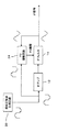
図1は、チューナの要部を示すブロックである。アンテナで受信されたRF信号は、ミキサ10に供給される。ミキサ10には、希望局信号とIF信号の周波数分離れたローカル信号が供給されており、希望局信号がIF信号の周波数にダウンコンバートされたフィルタ前のIF信号が得られる。このIF信号は、IFアンプ12において所定の増幅がなされた後、IFフィルタ14に供給される。
FIG. 1 is a block diagram showing the main part of the tuner. The RF signal received by the antenna is supplied to the
そして、このIFフィルタ14において、IF信号の中心周波数付近の希望局信号が抽出され、これが後段に供給され、復調され再生される。
In the
また、IFフィルタ14の出力のフィルタ後のIF信号は、Sメータ16に供給される。Sメータはフィルタ後のIF信号のレベルを検出し、検出結果をSメータ出力として、出力する。Sメータ出力は、希望局信号の受信強度レベルを示すものであり、ステレオモノラルの切り換え制御などに利用される。
Further, the filtered IF signal of the output of the
そして、本実施形態では、擬似正弦波生成回路20を有しており、ここにおいて擬似正弦波が生成される。そして、IFアンプ12と、ミキサ10との間にはスイッチ22が設けられている。このスイッチ22の切り換えによって、ミキサ10の出力と、擬似正弦波生成回路20からの擬似正弦波のいずれかをIFアンプ12に切り換えて入力ができる。
In this embodiment, a pseudo sine
本実施形態では、スイッチ22を切り換えて擬似正弦波をIFアンプ12に供給している状態において、IFフィルタ14の中心周波数F0の調整や、Sメータ16の検出レベルの調整を行う。
In the present embodiment, adjustment of the center frequency F0 of the
IFフィルタ14の出力であるフィルタ後のIF信号はF0調整回路24に供給される。このF0調整回路24には、IFアンプ12への入力信号である擬似正弦波も供給されている。F0調整回路はフィルタ後のIF信号と擬似正弦波の比較からIFフィルタ14の中心周波数F0を調整するためのF0調整信号を作成する。F0調整信号は、IFフィルタ14に供給され、IFフィルタのバンドパス中心周波数F0が調整される。
The filtered IF signal that is the output of the
また、Sメータ出力は、Sメータ調整回路26にも供給される。理想では、擬似正弦波の入力時には、Sメータ出力は予め決定された所定の値となるはずであるが、ばらつきにより誤差が生じる。Sメータ調整回路26は、Sメータ調整用信号を生成する。このSメータ調整用信号に応じて、Sメータ16における検出レベルが調整される。すなわち、擬似正弦波入力時におけるSメータ出力が所定値となるようにSメータ16の検出レベルが調整される。
The S meter output is also supplied to the S
本実施形態のチューナの回路は、半導体集積回路(IC、LSI)内に内蔵される。従って、IFフィルタ14は、セラミックフィルタではなく、フィルタリング特性について最適化する調整が必要となる。なお、IFフィルタ14は、アクティブでも、パッシブでもよい。
The tuner circuit of this embodiment is built in a semiconductor integrated circuit (IC, LSI). Therefore, the
<擬似正弦波>
ここで、擬似正弦波生成回路20において生成される擬似正弦波について説明する。擬似正弦波は、例えば図2(c)に示すようなものであり、単なる矩形波ではなく、少なくとも片側2段階のレベル変化を有している。このような疑似正弦波は、デジタル回路による矩形波信号の合成により生成される。例えば、同一のクロック周波数を用いて作成される図2(a)の矩形波と、図2(b)の矩形波を加算することで、図2(c)の片側2段階変化の疑似正弦波が生成される。このような論理演算によって得られたデジタルデータをDACによりアナログの擬似正弦波として、IFアンプ12に供給すればよい。
<Pseudo sine wave>
Here, the pseudo sine wave generated in the pseudo sine
<F0の調整>
IFフィルタ14のF0調整では、スイッチ22を切り換え、擬似正弦波生成回路20において生成した疑似正弦波をIFアンプ12およびF0調整回路24に入力する。F0調整回路24では、IFフィルタ14の出力との位相を比較して、この比較に基づいて、IFフィルタ14の中心周波数F0を調整する。
<F0 adjustment>
In the F0 adjustment of the
IFフィルタ14の中心周波数F0の調整の概念図を図3に示す。スイッチ22によりRF信号を入力するモードから、疑似正弦波を入力するモードに切り換える。これによって、疑似正弦波がIFアンプ12に入力される。この結果として、IFフィルタ14の出力に、IFアンプ12、IFフィルタ14を通過した信号が出力される。この信号は、フィルタリングによって、変化部分がなまり正弦波に近い波形になっている。
A conceptual diagram of the adjustment of the center frequency F0 of the
そして、擬似正弦波と、IFフィルタ14の出力信号がF0調整回路24に入力される。F0調整回路24は、IFフィルタ14のバンドパス中心周波数F0を調整する。
The pseudo sine wave and the output signal of the
F0調整回路24の構成例を図4に示す。この例において、F0調整回路24は、位相比較器242、論理回路244、F0調整用DAC246を含んでいる。そして、基準となる疑似正弦波とIFフィルタを通過後の出力信号が位相比較器242に入力され、ここで両者位相比較が行われる。すなわち、両信号の周波数が同一であれば、位相は合致するはずであり、その位相比較結果についての信号が論理回路244に供給される。論理回路244は、位相比較結果を基に、F0調整用DAC246を書き換える。従って、F0調整回路用DAC246が書き換えられた値に応じたF0調整信号をIFフィルタ14に供給する。従って、位相比較結果に応じて、IFフィルタの中心周波数F0が変更される。この調整を繰り返していき、IFフィルタ14の中心周波数F0を最適値となるよう追い込み、最終的にIFフィルタ14の中心周波数F0を最適値に設定できる。
A configuration example of the
このようなF0調整動作は、工場で出荷前に行ってもよいが、電源オン時に毎回行うことや、温度などの環境情報を元に所望のタイミングで再調整を行ったり、定期的に再調整を行ったりすることもできる。また、F0調整用DAC246の最終出力をEEPROMなどの不揮発性メモリに書き込んでおくとよい。そして、通常はその不揮発性メモリに記憶されている値をF0調整用DACに供給し、上述の調整動作を行った場合に不揮発性メモリの値を書き換えることが好適である。
Such F0 adjustment operation may be performed at the factory before shipment, but is performed every time the power is turned on, readjustment is performed at a desired timing based on environmental information such as temperature, and readjustment is performed periodically. You can also do. The final output of the
ここで、擬似正弦波生成回路20において生成される擬似正弦波は、例えば図2(c)に示すようなものである。単なる矩形波ではなく、少なくとも片側2段階のレベル変化を有している。このような擬似正弦波を用いることで、所定次数の高調波を相殺して高調波を抑制することができる。矩形波を用いると、高調波が比較的大きくなり、これによってIF周波数が変動してしまいやすい。一方、擬似正弦波を用いることで、正確なF0調整が行える。なお、さらにレベル数を増加して、正弦波に近づけることも好適であるが、図2(c)の波形が生成しやすさの面から好ましい。
Here, the pseudo sine wave generated in the pseudo sine
<Sメータの調整>
Sメータ16の検出レベル調整においても、生成した疑似正弦波を信号処理経路に入力する。
<Adjustment of S meter>
Also in the detection level adjustment of the
Sメータ16の検出レベル調整の概念図を図5に示す。まず、スイッチ22を切り換えて、RF信号を受信するモードから、擬似正弦波生成回路20からの疑似正弦波をIFアンプ12に入力するモードに切り換える。これによって、疑似正弦波がIFアンプ12に入力され、この出力がIFフィルタ14においてフィルタリングされた信号が得られる。
A conceptual diagram of detection level adjustment of the
このフィルタ後の信号がSメータ16に入力され、IFフィルタ14を通過後の信号のレベル検出の結果が出力される。擬似正弦波は、その信号レベルは予めわかっている。そこで、Sメータ調整回路26は、このときのレベル検出の結果がある一定の値になるように調整を加える。
The filtered signal is input to the
例えば、図6において実線で示す特性が正しい特性であるとする。擬似正弦波を入力した場合における特性が破線で示すような特性であった場合、これを実線で示す特性になるようにSメータ調整回路26がメータ調整信号を生成する。
For example, assume that the characteristic indicated by the solid line in FIG. 6 is the correct characteristic. When the characteristic when the pseudo sine wave is input is a characteristic as indicated by a broken line, the S
このようなSメータの調整動作も、工場で出荷前に行ってもよいが、電源オン時に毎回行うことや、温度などの環境情報を元に所望のタイミングで再調整を行ったり、定期的に再調整を行ったりすることもできる。また、Sメータ調整回路26の最終出力をEEPROMなどの不揮発性メモリに書き込んでおき、通常はその不揮発性メモリに記憶されている値を用い、上述の調整動作を行った場合に、この値を書き換えることも好適である。
Such an adjustment operation of the S meter may be performed at the factory before shipment, but is performed every time the power is turned on, readjusted at a desired timing based on environmental information such as temperature, or periodically You can also readjust. In addition, when the final output of the S
このように、本実施形態によれば、上述のようにして、IFフィルタ14のF0調整及びSメータ16の検出レベル調整を行うことができる。
Thus, according to the present embodiment, the F0 adjustment of the
IFフィルタ14のF0調整では、従来のレプリカ発振回路を用いた間接的な調整方法にくらべ、実際のIFフィルタ14へ信号を通過させ調整作業を行うことで、精度を向上することができる。
In the F0 adjustment of the
また、Sメータ16の検出レベルの調整では、内部生成の信号により、Sメータ16のレベル検出の調整を行うことで、外部信号の入力無しにSメータ16のばらつき調整を行い、Sメータ出力のばらつきを低減することができる。
Further, in the adjustment of the detection level of the
10 ミキサ、12 アンプ、14 IFフィルタ、16 Sメータ、20 擬似正弦波生成回路、22 スイッチ、24 F0調整回路、26 Sメータ調整回路、242 位相比較器、244 論理回路、246 F0調整用DAC。 10 mixer, 12 amplifier, 14 IF filter, 16 S meter, 20 pseudo sine wave generation circuit, 22 switch, 24 F0 adjustment circuit, 26 S meter adjustment circuit, 242 phase comparator, 244 logic circuit, 246 F0 adjustment DAC.
Claims (4)
ダウンコンバートされた信号を中心周波数F0を中心としてフィルタリングしてIF信号を取り出すIFフィルタと、
正負両側においてそれぞれ少なくとも2段階のレベル変化を有する擬似正弦波を生成する擬似正弦波生成回路と、
ダウンコンバートされた信号に代えて、前記擬似正弦波を前記IFフィルタに供給するスイッチ回路と、
IFフィルタの中心周波数F0を調整するF0調整回路と、
を有し、
前記スイッチ回路により擬似正弦波を前記IFフィルタに通過させ、この状態で前記F0調整回路が、前記擬似正弦波の位相と前記IFフィルタ通過後の信号の位相を比較し、その比較結果に応じて、前記IFフィルタにおける中心周波数F0を調整することを特徴とするチューナ。 In a tuner that performs signal processing by down-converting an RF signal to an IF signal,
An IF filter for filtering the down-converted signal around the center frequency F0 and extracting an IF signal;
A pseudo sine wave generation circuit that generates a pseudo sine wave having at least two levels of change on both the positive and negative sides;
A switch circuit for supplying the pseudo sine wave to the IF filter instead of the down-converted signal;
An F0 adjustment circuit for adjusting the center frequency F0 of the IF filter;
Have
The switch circuit allows a pseudo sine wave to pass through the IF filter. In this state, the F0 adjustment circuit compares the phase of the pseudo sine wave with the phase of the signal after passing through the IF filter , and according to the comparison result. A tuner characterized by adjusting a center frequency F0 in the IF filter.
さらに、
IFフィルタの出力の信号レベルを検出するSメータと、
Sメータの出力を調整するSメータ調整回路と、
を有し、
前記スイッチ回路により擬似正弦波を前記IFフィルタに通過させ、この状態で前記Sメータの出力信号のレベルから、前記Sメータの検出レベルを調整することを特徴とするチューナ。 The tuner according to claim 1, wherein
further,
An S meter for detecting the signal level of the output of the IF filter;
An S meter adjustment circuit for adjusting the output of the S meter;
Have
A tuner characterized in that a pseudo sine wave is passed through the IF filter by the switch circuit and the detection level of the S meter is adjusted from the level of the output signal of the S meter in this state.
通常モードにおいて、RF信号をローカルの正弦波とミキシングするミキサー回路によって得られる、ダウンコンバートされた信号を中心周波数F0を中心としてフィルタリングしてIF信号を取り出すIFフィルタと、 An IF filter that obtains an IF signal by filtering the downconverted signal around the center frequency F0, obtained by a mixer circuit that mixes the RF signal with a local sine wave in the normal mode;
ローカルの正弦波とは異なっていて、正負両側においてそれぞれ少なくとも2段階のレベル変化を有する擬似正弦波を生成する擬似正弦波生成回路と、 A pseudo sine wave generating circuit that generates a pseudo sine wave that is different from a local sine wave and has at least two levels of level changes on both positive and negative sides;
チューナの調整モード時に、ダウンコンバートされた信号を前記IFフィルタに供給し、チューナの調整モード時に、ダウンコンバートされた信号に代えて、前記擬似正弦波を前記IFフィルタに供給するスイッチ回路と、 A switch circuit that supplies a down-converted signal to the IF filter in a tuner adjustment mode, and supplies the pseudo sine wave to the IF filter in place of the down-converted signal in a tuner adjustment mode;
IFフィルタの中心周波数F0を調整するF0調整回路と、 An F0 adjustment circuit for adjusting the center frequency F0 of the IF filter;
を有し、 Have
チューナの調整モード時に、前記スイッチ回路の状態により前記IFフィルタには前記擬似正弦波生成回路からの前記擬似正弦波が入力され、前記擬似正弦波が前記IFフィルタに入力されるという状態下で、前記F0調整回路が、前記IFフィルタに入力される前記擬似正弦波の位相と前記IFフィルタの出力信号の位相を比較し、その比較結果に応じて、前記IFフィルタにおける中心周波数F0を調整することを特徴とするチューナ。 In the tuner adjustment mode, the pseudo sine wave from the pseudo sine wave generation circuit is input to the IF filter according to the state of the switch circuit, and the pseudo sine wave is input to the IF filter. The F0 adjustment circuit compares the phase of the pseudo sine wave input to the IF filter with the phase of the output signal of the IF filter, and adjusts the center frequency F0 in the IF filter according to the comparison result. A tuner characterized by
さらに、 further,
IFフィルタの出力の信号レベルを検出するSメータと、 An S meter for detecting the signal level of the output of the IF filter;
Sメータの出力を調整するSメータ調整回路と、 An S meter adjustment circuit for adjusting the output of the S meter;
を有し、 Have
チューナの調整モード時に、前記スイッチ回路の状態により前記IFフィルタには前記擬似正弦波生成回路からの前記擬似正弦波が入力され、前記擬似正弦波が前記IFフィルタに入力されるという状態下で、前記Sメータ調整回路は、前記Sメータの出力信号のレベルから、前記Sメータの検出レベルを調整することを特徴とするチューナ。 In the tuner adjustment mode, the pseudo sine wave from the pseudo sine wave generation circuit is input to the IF filter according to the state of the switch circuit, and the pseudo sine wave is input to the IF filter. The S meter adjustment circuit adjusts a detection level of the S meter from a level of an output signal of the S meter.
Priority Applications (3)
| Application Number | Priority Date | Filing Date | Title |
|---|---|---|---|
| JP2012098023A JP6078868B2 (en) | 2012-04-23 | 2012-04-23 | Tuner |
| EP13164772.9A EP2658121B1 (en) | 2012-04-23 | 2013-04-22 | Tuner with calibration of center frequency of IF notch filter and calibration of S-Meter |
| US13/868,640 US8855589B2 (en) | 2012-04-23 | 2013-04-23 | Tuner |
Applications Claiming Priority (1)
| Application Number | Priority Date | Filing Date | Title |
|---|---|---|---|
| JP2012098023A JP6078868B2 (en) | 2012-04-23 | 2012-04-23 | Tuner |
Publications (2)
| Publication Number | Publication Date |
|---|---|
| JP2013225814A JP2013225814A (en) | 2013-10-31 |
| JP6078868B2 true JP6078868B2 (en) | 2017-02-15 |
Family
ID=48877003
Family Applications (1)
| Application Number | Title | Priority Date | Filing Date |
|---|---|---|---|
| JP2012098023A Active JP6078868B2 (en) | 2012-04-23 | 2012-04-23 | Tuner |
Country Status (3)
| Country | Link |
|---|---|
| US (1) | US8855589B2 (en) |
| EP (1) | EP2658121B1 (en) |
| JP (1) | JP6078868B2 (en) |
Family Cites Families (10)
| Publication number | Priority date | Publication date | Assignee | Title |
|---|---|---|---|---|
| US5982228A (en) * | 1995-07-14 | 1999-11-09 | Lucent Technologies Inc | Frequency tuning apparatus and method for continuous-time filters |
| JP2002232251A (en) | 2001-02-01 | 2002-08-16 | Asahi Kasei Microsystems Kk | Device and method for adjusting filter center frequency |
| GB0117578D0 (en) * | 2001-07-19 | 2001-09-12 | Zarlink Semiconductor Ltd | Tuner |
| JP2004336152A (en) * | 2003-04-30 | 2004-11-25 | Sony Corp | Sine wave generating circuit |
| JP2005079677A (en) * | 2003-08-28 | 2005-03-24 | Sanyo Electric Co Ltd | Signal processing circuit for tuner |
| JP2005167660A (en) * | 2003-12-03 | 2005-06-23 | Matsushita Electric Ind Co Ltd | Semiconductor device |
| JP4282490B2 (en) * | 2004-01-06 | 2009-06-24 | パナソニック株式会社 | Filter automatic adjustment device and communication device |
| JP4829848B2 (en) * | 2007-07-26 | 2011-12-07 | オンセミコンダクター・トレーディング・リミテッド | Receiver device, field strength meter characteristic correction method, program |
| JP2009105727A (en) * | 2007-10-24 | 2009-05-14 | Sanyo Electric Co Ltd | Fm receiver |
| JP5787551B2 (en) * | 2011-02-28 | 2015-09-30 | ラピスセミコンダクタ株式会社 | Signal receiving apparatus and signal receiving method |
-
2012
- 2012-04-23 JP JP2012098023A patent/JP6078868B2/en active Active
-
2013
- 2013-04-22 EP EP13164772.9A patent/EP2658121B1/en active Active
- 2013-04-23 US US13/868,640 patent/US8855589B2/en active Active
Also Published As
| Publication number | Publication date |
|---|---|
| JP2013225814A (en) | 2013-10-31 |
| EP2658121B1 (en) | 2017-05-03 |
| US8855589B2 (en) | 2014-10-07 |
| EP2658121A3 (en) | 2015-10-07 |
| US20130285714A1 (en) | 2013-10-31 |
| EP2658121A2 (en) | 2013-10-30 |
Similar Documents
| Publication | Publication Date | Title |
|---|---|---|
| US8451971B2 (en) | Communication systems, clock generation circuits thereof, and method for generating clock signal | |
| US20140093019A1 (en) | Receiver | |
| CN108063618B (en) | VCO automatic calibration circuit and method | |
| CN102118131A (en) | Method for shortening start time of crystal oscillator | |
| CN108108153A (en) | Randomizer and the method with adjustable metastable constant voltage generation random number | |
| JP2005303650A (en) | Receiver | |
| US9118459B2 (en) | Wireless communication device and activation method of the wireless communication device | |
| KR20180026957A (en) | Duty correction device and semiconductor device including the same | |
| US9225341B2 (en) | Automatic amplitude control circuit | |
| JP2007006260A (en) | Agc circuit | |
| US9094021B2 (en) | Semiconductor device and variation information obtaining program | |
| JP6078868B2 (en) | Tuner | |
| US20150130542A1 (en) | Device and method for controlling output amplitude of voltage control oscillator in electronic device | |
| JP2012032275A (en) | Receiver circuit for radio time piece | |
| JP4010231B2 (en) | Radio receiver, radio clock, and repeater | |
| JP2011135536A (en) | Integrated circuit for temperature compensated crystal oscillation control | |
| US8952761B2 (en) | System and method for supporting different types of oscillator circuits | |
| US7348807B2 (en) | Electric circuit for providing a selection signal | |
| JP2001339317A (en) | Transmission output control circuit for radio communication equipment | |
| TWI685219B (en) | Receiving circuit of wireless communication system and method of receiving rf signal | |
| KR102135426B1 (en) | Operation mode setting circuit of semiconductor apparatus and data processing system using the same | |
| JP2013119725A (en) | Rssi signal detecting error preventing circuit | |
| CN102598517A (en) | Semiconductor integrated circuit and receiving apparatus | |
| JP2007116247A (en) | Orthogonal signal generation circuit and reception tuner having the same, and communication equipment | |
| US20130148444A1 (en) | Data reading device |
Legal Events
| Date | Code | Title | Description |
|---|---|---|---|
| A621 | Written request for application examination |
Free format text: JAPANESE INTERMEDIATE CODE: A621 Effective date: 20150421 |
|
| RD02 | Notification of acceptance of power of attorney |
Free format text: JAPANESE INTERMEDIATE CODE: A7422 Effective date: 20160201 |
|
| RD04 | Notification of resignation of power of attorney |
Free format text: JAPANESE INTERMEDIATE CODE: A7424 Effective date: 20160204 |
|
| A977 | Report on retrieval |
Free format text: JAPANESE INTERMEDIATE CODE: A971007 Effective date: 20160229 |
|
| A131 | Notification of reasons for refusal |
Free format text: JAPANESE INTERMEDIATE CODE: A131 Effective date: 20160308 |
|
| A521 | Request for written amendment filed |
Free format text: JAPANESE INTERMEDIATE CODE: A523 Effective date: 20160607 |
|
| TRDD | Decision of grant or rejection written | ||
| A01 | Written decision to grant a patent or to grant a registration (utility model) |
Free format text: JAPANESE INTERMEDIATE CODE: A01 Effective date: 20161129 |
|
| A61 | First payment of annual fees (during grant procedure) |
Free format text: JAPANESE INTERMEDIATE CODE: A61 Effective date: 20161227 |
|
| R150 | Certificate of patent or registration of utility model |
Ref document number: 6078868 Country of ref document: JP Free format text: JAPANESE INTERMEDIATE CODE: R150 |
|
| R250 | Receipt of annual fees |
Free format text: JAPANESE INTERMEDIATE CODE: R250 |
|
| R250 | Receipt of annual fees |
Free format text: JAPANESE INTERMEDIATE CODE: R250 |
|
| R250 | Receipt of annual fees |
Free format text: JAPANESE INTERMEDIATE CODE: R250 |
|
| R250 | Receipt of annual fees |
Free format text: JAPANESE INTERMEDIATE CODE: R250 |
|
| R250 | Receipt of annual fees |
Free format text: JAPANESE INTERMEDIATE CODE: R250 |