JP6064861B2 - Method for manufacturing thermoelectric conversion device - Google Patents
Method for manufacturing thermoelectric conversion device Download PDFInfo
- Publication number
- JP6064861B2 JP6064861B2 JP2013212413A JP2013212413A JP6064861B2 JP 6064861 B2 JP6064861 B2 JP 6064861B2 JP 2013212413 A JP2013212413 A JP 2013212413A JP 2013212413 A JP2013212413 A JP 2013212413A JP 6064861 B2 JP6064861 B2 JP 6064861B2
- Authority
- JP
- Japan
- Prior art keywords
- thermoelectric conversion
- back surface
- surface pattern
- insulating base
- base material
- Prior art date
- Legal status (The legal status is an assumption and is not a legal conclusion. Google has not performed a legal analysis and makes no representation as to the accuracy of the status listed.)
- Active
Links
Images


Classifications
-
- H—ELECTRICITY
- H10—SEMICONDUCTOR DEVICES; ELECTRIC SOLID-STATE DEVICES NOT OTHERWISE PROVIDED FOR
- H10N—ELECTRIC SOLID-STATE DEVICES NOT OTHERWISE PROVIDED FOR
- H10N10/00—Thermoelectric devices comprising a junction of dissimilar materials, i.e. devices exhibiting Seebeck or Peltier effects
- H10N10/80—Constructional details
- H10N10/81—Structural details of the junction
- H10N10/817—Structural details of the junction the junction being non-separable, e.g. being cemented, sintered or soldered
-
- H—ELECTRICITY
- H10—SEMICONDUCTOR DEVICES; ELECTRIC SOLID-STATE DEVICES NOT OTHERWISE PROVIDED FOR
- H10N—ELECTRIC SOLID-STATE DEVICES NOT OTHERWISE PROVIDED FOR
- H10N10/00—Thermoelectric devices comprising a junction of dissimilar materials, i.e. devices exhibiting Seebeck or Peltier effects
- H10N10/01—Manufacture or treatment
Description
本発明は、熱電変換素子と配線パターンとが電気的、機械的に接続された熱電変換装置の製造方法に関するものである。 The present invention includes a thermoelectric conversion element and the wiring pattern is related to electrical, mechanically connected manufacturing method of the thermoelectric conversion equipment.
従来より、この種の熱電変換装置として、上部基板と下部基板との間に複数の熱電変換素子が配置され、当該複数の熱電変換素子が上部基板および下部基板に形成された配線パターンとはんだを介して電気的、機械的に接続されたものが提案されている(例えば、特許文献1参照)。 Conventionally, as this type of thermoelectric conversion device, a plurality of thermoelectric conversion elements are arranged between an upper substrate and a lower substrate, and the plurality of thermoelectric conversion elements are connected to a wiring pattern and solder formed on the upper substrate and the lower substrate. A device that is electrically and mechanically connected to each other has been proposed (for example, see Patent Document 1).
具体的には、この熱電変換装置では、配線パターン上にはNi、Pd、Pt、Nb、Cr、Ti等が積層された積層膜が形成されている。そして、積層膜がはんだと接合されている。なお、隣接する熱電変換素子の間は空洞とされている。 Specifically, in this thermoelectric conversion device, a laminated film in which Ni, Pd, Pt, Nb, Cr, Ti and the like are laminated is formed on the wiring pattern. The laminated film is bonded to the solder. In addition, it is made into the cavity between adjacent thermoelectric conversion elements.
これによれば、積層膜にて、はんだの濡れ性を向上させることができ、はんだと配線パターンとを強固に接合できる。また、熱電変換素子とはんだとの間にNi、Pd、Pt、Nb、Cr、Ti等が積層された積層膜を配置することにより、はんだと熱電変換素子とを強固に接合できる。 According to this, the wettability of solder can be improved by the laminated film, and the solder and the wiring pattern can be firmly joined. Further, by arranging a laminated film in which Ni, Pd, Pt, Nb, Cr, Ti, etc. are laminated between the thermoelectric conversion element and the solder, the solder and the thermoelectric conversion element can be firmly joined.
上記熱電変換装置は、次のように製造される。まず、焼結等によって形成された熱電変換素子を用意し、はんだと接触する部分に積層膜を形成する。また、下部基板および上部基板に、それぞれ配線パターンを形成すると共に、配線パターン上に積層膜を形成する。そして、下部基板上にはんだを介して熱電変換素子を配置すると共に、熱電変換素子上にはんだを介して上部基板を配置する。その後、はんだリフロー等を行い、はんだを介して積層膜と熱電変換素子とを電気的、機械的に接続することにより、製造される。 The thermoelectric conversion device is manufactured as follows. First, a thermoelectric conversion element formed by sintering or the like is prepared, and a laminated film is formed on a portion in contact with solder. In addition, a wiring pattern is formed on each of the lower substrate and the upper substrate, and a laminated film is formed on the wiring pattern. Then, the thermoelectric conversion element is disposed on the lower substrate via the solder, and the upper substrate is disposed on the thermoelectric conversion element via the solder. Then, it manufactures by performing solder reflow etc. and electrically and mechanically connecting a laminated film and a thermoelectric conversion element via solder.
しかしながら、上記熱電変換装置では、はんだを用いており、はんだの濡れ性を向上させるための積層膜も必要となる。このため、部品点数が増加すると共に構造が複雑となり、ひいてはコストが高くなるという問題がある。 However, the thermoelectric conversion device uses solder, and a laminated film for improving the wettability of the solder is also required. For this reason, there is a problem that the number of parts increases, the structure becomes complicated, and the cost increases.
本発明は上記点に鑑みて、簡素な構成で熱電変換素子と配線パターンとを電気的、機械的に接続できる熱電変換装置の製造方法を提供することを目的とする。 The present invention is made in view of the above disadvantages, and an object thereof is to provide an electrical method of mechanically connected can thermoelectric conversion equipment to the thermoelectric conversion element and the wiring pattern with a simple configuration.
上記目的を達成するため、請求項1に記載の発明では、熱可塑性樹脂を含んで構成されており、厚さ方向に貫通する複数のビアホール(11、12)が形成され、前記ビアホールに複数の金属原子が所定の結晶構造を維持している合金の粉末に有機溶剤を加えてペースト化した導電性ペースト(41、51)が充填されている絶縁基材(10)を用意する工程と、前記絶縁基材の表面(10a)に所定の前記導電性ペーストと接触する表面パターン(21)を有する表面保護部材(20)を配置すると共に、前記絶縁基材の裏面(10b)に所定の前記導電性ペーストと接触する裏面パターン(31)を有する裏面保護部材(30)を配置して積層体(90)を形成する工程と、前記積層体を加熱しながら積層方向から加圧し、前記導電性ペーストから熱電変換素子(40、50)を形成しつつ、前記熱電変換素子を構成する金属原子および前記表面パターンを構成する金属原子が拡散して構成される合金層(71)を形成すると共に前記熱電変換素子を構成する金属原子および前記裏面パターンを構成する金属原子が拡散して構成される合金層(72)を形成し、前記熱電変換素子と、前記表面パターンおよび前記裏面パターンとを前記合金層を介して電気的、機械的に接続する一体化工程と、を行うものであり、前記一体化工程では、前記積層体を加熱して前記導電性ペーストに含まれる前記有機溶剤を蒸発させる工程と、前記絶縁基材を構成する熱可塑性樹脂の軟化点以上の温度に前記積層体を加熱しながら前記積層方向から加圧し、前記熱電変換素子と、前記表面パターンおよび前記裏面パターンとを前記合金層を介して電気的、機械的に接続する工程と、前記積層方向からの加圧を保持しつつ、前記積層体を冷却して前記積層体を一体化する工程と、を行うことを特徴としている。
これによれば、はんだを用いる必要がなく、はんだを用いるために必要な積層膜を形成する必要がない。また、熱電変換素子と表面パターンおよび裏面パターンとの界面に形成される合金層は、熱電変換素子と表面パターンおよび裏面パターンを構成する金属原子にて形成されている。つまり、熱電変換素子と表面パターンおよび裏面パターンとの界面に別の部材を配置する必要がない。このため、部品点数を削減することによって構成を簡素化でき、ひいてはコストの低減を図ることができる。
また、熱電変換素子を形成しつつ、熱電変換素子と表面パターンおよび裏面パターンとの界面に合金層を形成している。このため、加圧した際に熱電変換素子が割れることを抑制できる
In order to achieve the above object, the invention according to
According to this, it is not necessary to use solder, and it is not necessary to form a laminated film necessary for using solder. Further, the alloy layer formed at the interface between the thermoelectric conversion element and the surface pattern and the back surface pattern is formed of metal atoms constituting the thermoelectric conversion element, the surface pattern, and the back surface pattern. That is, it is not necessary to arrange another member at the interface between the thermoelectric conversion element and the front and back patterns. For this reason, the configuration can be simplified by reducing the number of parts, and the cost can be reduced.
Moreover, the alloy layer is formed in the interface of a thermoelectric conversion element, a surface pattern, and a back surface pattern, forming a thermoelectric conversion element. For this reason, it can suppress that a thermoelectric conversion element breaks when it pressurizes.
また、請求項4に記載の発明では、熱可塑性樹脂を含んで構成されており、厚さ方向に貫通する複数のビアホール(11、12)が形成され、前記ビアホールに熱電変換素子(40、50)が埋め込まれた絶縁基材(10)を用意する工程と、前記絶縁基材の表面(10a)に所定の前記熱電変換素子と接触する表面パターン(21)を有する表面保護部材(20)を配置すると共に、前記絶縁基材の裏面(10b)に所定の前記熱電変換素子と接触する裏面パターン(31)を有する裏面保護部材(30)を配置して積層体(90)を形成する工程と、前記積層体を加熱しながら積層方向から加圧し、前記熱電変換素子を構成する金属原子および前記表面パターンを構成する金属原子が拡散して構成される合金層(71)を形成すると共に前記熱電変換素子を構成する金属原子および前記裏面パターンを構成する金属原子が拡散して構成される合金層(72)を形成し、前記熱電変換素子と、前記表面パターンおよび前記裏面パターンとを前記合金層を介して電気的、機械的に接続する一体化工程と、を行うものであり、前記一体化工程では、前記絶縁基材を構成する熱可塑性樹脂の軟化点以上の温度に前記積層体を加熱しながら前記積層方向から加圧し、前記熱電変換素子と、前記表面パターンおよび前記裏面パターンとを前記合金層を介して電気的、機械的に接続する工程と、前記積層方向からの加圧を保持しつつ、前記積層体を冷却して前記積層体を一体化する工程と、を行うことを特徴としている。
これによれば、熱電変換素子は絶縁基材に形成されたビアホールに埋め込まれているため、一体化工程では、熱電変換素子に生じる応力のうち積層方向と垂直方向の成分を絶縁基材によって相殺できる。このため、熱電変換素子が積層方向と垂直方向に割れることを抑制できる。
Further, in the invention described in claim 4 , it is configured to include a thermoplastic resin, and a plurality of via holes (11, 12) penetrating in the thickness direction are formed, and thermoelectric conversion elements (40, 50) are formed in the via holes. And a surface protection member (20) having a surface pattern (21) in contact with the predetermined thermoelectric conversion element on the surface (10a) of the insulating substrate. And a step of forming a laminate (90) by disposing a back surface protection member (30) having a back surface pattern (31) in contact with the predetermined thermoelectric conversion element on the back surface (10b) of the insulating base. And pressurizing the laminated body from the laminating direction to form an alloy layer (71) constituted by diffusing metal atoms constituting the thermoelectric conversion element and metal atoms constituting the surface pattern. An alloy layer (72) formed by diffusing metal atoms constituting the thermoelectric conversion element and metal atoms constituting the back surface pattern is formed, and the thermoelectric conversion element, the surface pattern, and the back surface pattern are An integration step of electrically and mechanically connecting via an alloy layer, and in the integration step, the laminate is heated to a temperature equal to or higher than a softening point of a thermoplastic resin constituting the insulating base. Pressurizing from the laminating direction while heating, and electrically and mechanically connecting the thermoelectric conversion element, the front surface pattern and the back surface pattern through the alloy layer, and pressurizing from the laminating direction The step of cooling the laminated body and integrating the laminated body is performed while holding the film.
According to this, since the thermoelectric conversion element is embedded in the via hole formed in the insulating base material, in the integration process, the stress in the thermoelectric conversion element is offset by the insulating base material in the direction perpendicular to the stacking direction. it can. For this reason, it can suppress that a thermoelectric conversion element cracks in a perpendicular direction with a lamination direction.
また、請求項9に記載の発明では、熱可塑性樹脂を含んで構成されており、厚さ方向に貫通する複数のビアホール(11、12)が形成され、前記ビアホールに複数の金属原子が所定の結晶構造を維持している合金の粉末に有機溶剤を加えてペースト化した導電性ペースト(41、51)が充填されている絶縁基材(10)を用意する工程と、前記絶縁基材の表面(10a)に所定の前記導電性ペーストと接触する表面パターン(21)を有する表面保護部材(20)を配置すると共に、前記絶縁基材の裏面(10b)に所定の前記導電性ペーストと接触する裏面パターン(31)を有する裏面保護部材(30)を配置して積層体(90)を形成する工程と、前記積層体を加熱しながら積層方向から加圧し、前記導電性ペーストから熱電変換素子(40、50)を形成しつつ、前記熱電変換素子を構成する金属原子および前記表面パターンを構成する金属原子が拡散して構成される合金層(71)を形成すると共に前記熱電変換素子を構成する金属原子および前記裏面パターンを構成する金属原子が拡散して構成される合金層(72)を形成し、前記熱電変換素子と、前記表面パターンおよび前記裏面パターンとを前記合金層を介して電気的、機械的に
接続する一体化工程と、を行うものであり、前記積層体を形成する工程の前には、前記絶縁基材に空隙(13)が形成されており、前記一体化工程では、前記熱可塑性樹脂を前記空隙に流動させつつ、前記熱電変換素子および前記合金層を形成することを特徴としている。
In the invention described in claim 9 , a plurality of via holes (11, 12) penetrating in the thickness direction are formed, and a plurality of metal atoms are provided in the via holes in a predetermined manner. A step of preparing an insulating substrate (10) filled with a conductive paste (41, 51) obtained by adding an organic solvent to a powder of an alloy maintaining a crystal structure, and a surface of the insulating substrate; A surface protection member (20) having a surface pattern (21) in contact with the predetermined conductive paste is disposed on (10a), and the predetermined conductive paste is in contact with the back surface (10b) of the insulating substrate. A step of forming a laminated body (90) by disposing a back surface protection member (30) having a back surface pattern (31), and applying pressure from the laminating direction while heating the laminated body to convert thermoelectric from the conductive paste While forming a child (40, 50), an alloy layer (71) formed by diffusing metal atoms constituting the thermoelectric conversion element and metal atoms constituting the surface pattern is formed, and the thermoelectric conversion element is formed An alloy layer (72) is formed by diffusing metal atoms constituting the rear surface pattern and metal atoms constituting the back surface pattern, and the thermoelectric conversion element, the front surface pattern and the back surface pattern are interposed via the alloy layer. An integration step of electrically and mechanically connecting, and before the step of forming the laminate, a gap (13) is formed in the insulating base material, and the integration step Then, the thermoelectric conversion element and the alloy layer are formed while allowing the thermoplastic resin to flow into the gap.
また、請求項10に記載の発明では、熱可塑性樹脂を含んで構成されており、厚さ方向に貫通する複数のビアホール(11、12)が形成され、前記ビアホールに複数の金属原子が所定の結晶構造を維持している合金の粉末に有機溶剤を加えてペースト化した導電性ペースト(41、51)が充填されている絶縁基材(10)を用意する工程と、前記絶縁基材の表面(10a)に所定の前記導電性ペーストと接触する表面パターン(21)を有する表面保護部材(20)を配置すると共に、前記絶縁基材の裏面(10b)に所定の前記導電性ペーストと接触する裏面パターン(31)を有する裏面保護部材(30)を配置して積層体(90)を形成する工程と、前記積層体を加熱しながら積層方向から加圧し、前記導電性ペーストから熱電変換素子(40、50)を形成しつつ、前記熱電変換素子を構成する金属原子および前記表面パターンを構成する金属原子が拡散して構成される合金層(71)を形成すると共に前記熱電変換素子を構成する金属原子および前記裏面パターンを構成する金属原子が拡散して構成される合金層(72)を形成し、前記熱電変換素子と、前記表面パターンおよび前記裏面パターンとを前記合金層を介して電気的、機械的に接続する一体化工程と、を行うものであり、前記積層体を形成する工程では、前記表面保護部材および前記裏面保護部材として熱可塑性樹脂を含むものを用い、前記一体化工程では、前記絶縁基材の表面と対向する部分および前記絶縁基材の裏面と対向する部分の少なくとも一方に窪み部(100a)が形成された一対のプレス板(100)を用いて前記積層体を加圧し、前記表面保護部材および前記裏面保護部材を構成する熱可塑性樹脂の少なくとも一方を前記窪み部に流動させると共に前記絶縁基材を構成する熱可塑性樹脂を流動させつつ、前記熱電変換素子および前記合金層を形成することを特徴としている。
Further, in the invention according to
また、請求項11に記載の発明では、熱可塑性樹脂を含んで構成されており、厚さ方向に貫通する複数のビアホール(11、12)が形成され、前記ビアホールに熱電変換素子(40、50)が埋め込まれた絶縁基材(10)を用意する工程と、前記絶縁基材の表面(10a)に所定の前記熱電変換素子と接触する表面パターン(21)を有する表面保護部材(20)を配置すると共に、前記絶縁基材の裏面(10b)に所定の前記熱電変換素子と接触する裏面パターン(31)を有する裏面保護部材(30)を配置して積層体(90)を形成する工程と、前記積層体を加熱しながら積層方向から加圧し、前記熱電変換素子を構成する金属原子および前記表面パターンを構成する金属原子が拡散して構成される合金層(71)を形成すると共に前記熱電変換素子を構成する金属原子および前記裏面パターンを構成する金属原子が拡散して構成される合金層(72)を形成し、前記熱電変換素子と、前記表面パターンおよび前記裏面パターンとを前記合金層を介して電気的、機械的に接続する一体化工程と、を行うものであり、前記積層体を形成する工程の前には、前記絶縁基材に空隙(13)が形成されており、前記一体化工程では、前記熱可塑性樹脂を前記空隙に流動させつつ、前記熱電変換素子および前記合金層を形成することを特徴としている。
Further, in the invention according to
また、請求項12に記載の発明では、熱可塑性樹脂を含んで構成されており、厚さ方向に貫通する複数のビアホール(11、12)が形成され、前記ビアホールに熱電変換素子(40、50)が埋め込まれた絶縁基材(10)を用意する工程と、前記絶縁基材の表面(10a)に所定の前記熱電変換素子と接触する表面パターン(21)を有する表面保護部材(20)を配置すると共に、前記絶縁基材の裏面(10b)に所定の前記熱電変換素子と接触する裏面パターン(31)を有する裏面保護部材(30)を配置して積層体(90)を形成する工程と、前記積層体を加熱しながら積層方向から加圧し、前記熱電変換素子を構成する金属原子および前記表面パターンを構成する金属原子が拡散して構成される合金層(71)を形成すると共に前記熱電変換素子を構成する金属原子および前記裏面パターンを構成する金属原子が拡散して構成される合金層(72)を形成し、前記熱電変換素子と、前記表面パターンおよび前記裏面パターンとを前記合金層を介して電気的、機械的に接続する一体化工程と、を行うものであり、前記積層体を形成する工程では、前記表面保護部材および前記裏面保護部材として熱可塑性樹脂を含むものを用い、前記一体化工程では、前記絶縁基材の表面と対向する部分および前記絶縁基材の裏面と対向する部分の少なくとも一方に窪み部(100a)が形成された一対のプレス板(100)を用いて前記積層体を加圧し、前記表面保護部材および前記裏面保護部材を構成する熱可塑性樹脂の少なくとも一方を前記窪み部に流動させると共に前記絶縁基材を構成する熱可塑性樹脂を流動させつつ、前記熱電変換素子および前記合金層を形成することを特徴としている。
Further, in the invention described in
これら請求項9ないし12に記載の発明によれば、一体化工程において、導電性ペーストに印加される加圧力を大きくでき、熱電変換素子と表面パターンおよび裏面パターンとの間に合金層を形成し易くできる。 According to the inventions according to these ninth to twelfth aspects, in the integration step, the pressure applied to the conductive paste can be increased, and an alloy layer is formed between the thermoelectric conversion element and the front and back patterns. Easy to do.
なお、この欄および特許請求の範囲で記載した各手段の括弧内の符号は、後述する実施形態に記載の具体的手段との対応関係を示すものである。 In addition, the code | symbol in the bracket | parenthesis of each means described in this column and the claim shows the correspondence with the specific means as described in embodiment mentioned later.
以下、本発明の実施形態について図に基づいて説明する。なお、以下の各実施形態相互において、互いに同一もしくは均等である部分には、同一符号を付して説明を行う。 Hereinafter, embodiments of the present invention will be described with reference to the drawings. In the following embodiments, parts that are the same or equivalent to each other will be described with the same reference numerals.
(第1実施形態)
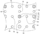
本発明の第1実施形態について図面を参照しつつ説明する。図1〜図3に示されるように、本実施形態の熱電変換装置1は、絶縁基材10、表面保護部材20、裏面保護部材30が一体化され、この一体化されたものの内部で異種金属である第1、第2層間接続部材40、50が交互に直列に接続されて構成されている。
(First embodiment)
A first embodiment of the present invention will be described with reference to the drawings. As shown in FIGS. 1 to 3, in the
なお、図1は、理解をし易くするために、表面保護部材20を省略して示してある。また、図1は、断面図ではないが、第1、第2層間接続部材40、50にハッチングを施してある。そして、本実施形態では、第1、第2層間接続部材40、50が本発明の熱電変換素子に相当している。
In FIG. 1, the
絶縁基材10は、本実施形態では、ポリエーテルエーテルケトン(PEEK)やポリエーテルイミド(PEI)を含む平面矩形状の熱可塑性樹脂フィルムによって構成されている。そして、この絶縁基材10には、厚さ方向に貫通する複数の第1、第2ビアホール11、12が互い違いになるように千鳥パターンに形成されている。
In this embodiment, the insulating
なお、本実施形態では、第1、第2ビアホール11、12が表面10aから裏面10bに向かって径が一定とされた円筒状とされているが、第1、第2ビアホール11、12は表面10aから裏面10bに向かって径が小さくなるテーパ状とされていてもよいし、角筒状とされていてもよい。
In the present embodiment, the first and second via
そして、第1ビアホール11には第1層間接続部材40が配置され、第2ビアホール12には第1層間接続部材40と異種金属となる第2層間接続部材50が配置されている。つまり、絶縁基材10には、第1、第2層間接続部材40、50が互い違いになるように配置されている。
A first
特に限定されるものではないが、例えば、第1層間接続部材40はP型を構成するBi−Sb−Te合金の粉末(金属粒子)を含む導電性ペーストから構成される。また、第2層間接続部材50はN型を構成するBi−Te合金の粉末(金属粒子)を含む導電性ペーストから構成される。
Although not particularly limited, for example, the first
絶縁基材10の表面10aには、ポリエーテルエーテルケトン(PEEK)やポリエーテルイミド(PEI)を含む平面矩形状の熱可塑性樹脂フィルムからなる表面保護部材20が配置されている。この表面保護部材20は、絶縁基材10と平面形状が同じ大きさとされており、絶縁基材10と対向する一面20a側に銅箔等がパターニングされた複数の表面パターン21が互いに離間するように形成されている。そして、各表面パターン21はそれぞれ第1、第2層間接続部材40、50と適宜電気的に接続されている。
On the
具体的には、隣接する1つの第1層間接続部材40と1つの第2層間接続部材50とを組60としたとき、各組60の第1、第2層間接続部材40、50は同じ表面パターン21と接続されている。つまり、各組60の第1、第2層間接続部材40、50は表面パターン21を介して電気的に接続されている。なお、本実施形態では、絶縁基材10の長辺方向(図1中紙面左右方向)に沿って隣接する1つの第1層間接続部材40と1つの第2層間接続部材50とが組60とされている。
Specifically, when one adjacent first
ここで、第1、第2層間接続部材40、50と表面パターン21との接続構造について説明する。図4に示されるように、第1、第2層間接続部材40、50と表面パターン21との界面(間)には、第1、第2層間接続部材40、50中の金属原子(Te)と表面パターン21中の金属原子(Cu)が拡散して構成されるCu−Te系の合金層71が形成されている。そして、第1、第2層間接続部材40、50と表面パターン21とは、合金層71を介して電気的、機械的に接続されている。
Here, a connection structure between the first and second
なお、ここでは、合金層71の構成をCu−Te系としたが、第1、第2層間接続部材40、50を構成する合金の粉末の配合比等により、例えば、合金層71の構成がCu−Biとされていてもよい。
Here, although the configuration of the
また、絶縁基材10の裏面10bには、ポリエーテルエーテルケトン(PEEK)やポリエーテルイミド(PEI)を含む熱可塑性樹脂フィルムからなる平面矩形状の裏面保護部材30が配置されている。この裏面保護部材30は、絶縁基材10と平面形状が同じ大きさとされており、絶縁基材10と対向する一面30a側に銅箔等がパターニングされた複数の裏面パターン31が互いに離間するように形成されている。そして、各裏面パターン31はそれぞれ第1、第2層間接続部材40、50と適宜電気的に接続されている。
In addition, on the
具体的には、隣接する組60において、一方の組60の第1層間接続部材40と、他方の組60の第2層間接続部材50とが同じ裏面パターン31と接続されている。つまり、組60を跨いで第1、第2層間接続部材40、50が裏面パターン31を介して電気的に接続されている。
Specifically, in the
本実施形態では、図2に示されるように、基本的には、絶縁基材10の長辺方向(図1中紙面左右方向)に沿って並んでいる2つの組60が隣接する組60とされている。また、図3に示されるように、絶縁基材10の外縁では、短辺方向(図1中紙面上下方向)に沿って並んでいる2つの組60が隣接する組60とされている。
In the present embodiment, as shown in FIG. 2, basically, two
したがって、第1、第2層間接続部材40、50は、絶縁基材10の長辺方向に交互に直列に接続されて折り返された後に再び長辺方向に交互に直列に接続される。つまり、第1、第2層間接続部材40、50は、折れ線状に交互に直列に接続されている。
Therefore, the first and second
ここで、第1、第2層間接続部材40、50と裏面パターン31との接続構造について説明する。図4に示されるように、第1、第2層間接続部材40、50と裏面パターン31との界面(間)には、第1、第2層間接続部材40、50と表面パターン21との間と同様に、第1、第2層間接続部材40、50中の金属原子(Te)と裏面パターン31中の金属原子(Cu)が拡散して構成されるCu−Te系の合金層72が形成されている。そして、第1、第2層間接続部材40、50と裏面パターン31とは、合金層72を介して電気的、機械的に接続されている。
Here, a connection structure between the first and second
なお、ここでは、合金層72の構成をCu−Te系としたが、第1、第2層間接続部材40、50を構成する合金の粉末の配合比等により、例えば、合金層72の構成がCu−Biとされていてもよい。
Here, although the configuration of the
また、図2、図3とは別断面において、裏面保護部材30には、裏面パターン31と電気的に接続されると共に、裏面保護部材30のうち絶縁基材10側と反対側の一面から露出する層間接続部材が形成されている。そして、裏面パターン31は、この層間接続部材を介して外部との電気的な接続が図れるようになっている。
2 and 3, the back
以上が本実施形態における熱電変換装置1の基本的な構成である。次に、上記熱電変換装置1の製造方法について図5を参照しつつ説明する。なお、図5は、図1中のII−II線に沿った断面図である。
The above is the basic configuration of the
まず、図5(a)に示されるように、絶縁基材10を用意し、複数の第1ビアホール11をドリル等によって形成する。
First, as shown in FIG. 5A, an insulating
次に、図5(b)に示されるように、各第1ビアホール11に第1導電性ペースト41を充填する。
Next, as shown in FIG. 5B, each first via
第1ビアホール11に第1導電性ペースト41を充填する方法(装置)としては、本出願人による特願2010−50356号に記載の方法(装置)を採用すると良い。
As a method (apparatus) for filling the first via
簡単に説明すると、吸着紙80を介して図示しない保持台上に、裏面10bが吸着紙80と対向するように絶縁基材10を配置する。なお、吸着紙80は、第1導電性ペースト41の有機溶剤を吸収できる材質のものであれば良く、一般的な上質紙等が用いられる。そして、第1導電性ペースト41を溶融させつつ、第1ビアホール11内に第1導電性ペースト41を充填する。これにより、第1導電性ペースト41の有機溶剤の大部分が吸着紙80に吸着され、第1ビアホール11に合金の粉末が密接して配置される。
Briefly, the insulating
第1導電性ペースト41としては、本実施形態では、金属原子が所定の結晶構造を維持している合金の粉末を融点が43℃であるパラフィン等の有機溶剤を加えてペースト化したものが用いられる。このため、第1導電性ペースト41を充填する際には、絶縁基材10の表面10aが約43℃に加熱された状態で行われる。なお、第1導電性ペースト41を構成する合金の粉末としては、例えば、メカニカルアロイにて形成されたBi−Sb−Te等が用いられる。
In the present embodiment, the first
続いて、図5(c)に示されるように、絶縁基材10に複数の第2ビアホール12をドリル等によって形成する。この第2ビアホール12は、上記のように、第1ビアホール11と互い違いとなり、第1ビアホール11と共に千鳥パターンを構成するように形成される。
Subsequently, as shown in FIG. 5C, a plurality of second via
次に、図5(d)に示されるように、再び、吸着紙80を介して図示しない保持台上に、裏面10bが吸着紙80と対向するように絶縁基材10を配置する。そして、第1導電性ペースト41を充填したときと同様に、第2ビアホール12内に第2導電性ペースト51を充填する。これにより、第2導電性ペースト51の有機溶剤の大部分が吸着紙80に吸着され、第2ビアホール12に合金の粉末が密接して配置される。
Next, as shown in FIG. 5D, the insulating
第2導電性ペースト51としては、本実施形態では、第1導電性ペースト41を構成する金属原子と異なる金属原子が所定の結晶構造を維持している合金の粉末を融点が常温であるテレピネ等の有機溶剤を加えてペースト化したものが用いられる。つまり、第2導電性ペースト51を構成する有機溶剤として、第1導電性ペースト41を構成する有機溶剤より融点が低いものが用いられる。そして、第2導電性ペースト51を充填する際には、絶縁基材10の表面10aが常温に保持された状態で行われる。言い換えると、第1導電性ペースト41に含まれる有機溶剤が固化された状態で、第2導電性ペースト51の充填が行われる。これにより、第1ビアホール11に第2導電性ペースト51が混入することが抑制される。
As the second
なお、第2導電性ペースト51を構成する合金の粉末としては、例えば、メカニカルアロイにて形成されたBi−Te等が用いられる。
In addition, as a powder of the alloy which comprises the 2nd
以上のようにして、第1、第2導電性ペースト41、51が充填された絶縁基材10を用意する。
As described above, the insulating
また、上記各工程とは別工程において、図5(e)および図5(f)に示されるように、表面保護部材20および裏面保護部材30のうち絶縁基材10と対向する一面20a、30aに銅箔等を形成する。そして、この銅箔を適宜パターニングすることにより、互いに離間している複数の表面パターン21が形成された表面保護部材20、互いに離間している複数の裏面パターン31が形成された裏面保護部材30を用意する。
Further, in steps different from the above steps, as shown in FIG. 5E and FIG. 5F, one
その後、図5(g)に示されるように、裏面保護部材30、絶縁基材10、表面保護部材20を順に積層して積層体90を構成する。具体的には、隣接する1つの第1ビアホール11に充填された第1導電性ペースト41と1つの第2ビアホール12に充填された第2導電性ペースト51とを組60としたとき、絶縁基材10の表面10a側に、組60毎の第1、第2導電性ペースト41、51が同じ表面パターン21に接触する状態で表面保護部材20を配置する。なお、本実施形態では、上記のように、絶縁基材10の長辺方向(図1紙面左右方向)に沿って隣接する1つの第1ビアホール11に充填された第1導電性ペースト41と1つの第2ビアホール12に充填された第2導電性ペースト51とが組60とされている。
Thereafter, as shown in FIG. 5G, the back
また、絶縁基材10の裏面10b側に、隣接する組60における一方の組60の第1導電性ペースト41および他方の組60の第2導電性ペースト51が同じ裏面パターン31に接触する状態で裏面保護部材30を配置する。なお、本実施形態では、上記のように、絶縁基材10の長辺方向(図1中紙面左右方向)に沿って並んでいる2つの組60が隣接する組60とされている。また、絶縁基材10の外縁では、短辺方向に沿って並んでいる2つの組60が隣接する組60とされている。
In the state where the first
続いて、図5(h)に示されるように、この積層体90を図示しない一対のプレス板の間に配置し、積層方向の上下両面から真空状態で加熱しながら加圧して積層体90を一体化する。なお、特に限定されるものではないが、積層体90を一体化する際には、積層体90とプレス板との間にロックウールペーパー等の緩衝材を配置してもよい。以下に、本実施形態の一体化工程について図6を参照しつつ具体的に説明する。
Subsequently, as shown in FIG. 5 (h), the
一体化工程は、図6に示されるように、まず、積層体90を約320℃まで加熱しながら時点T1まで0.1Mpaで加圧し、第1、第2導電性ペースト41、51に含まれる有機溶剤を蒸発させる。
In the integration step, as shown in FIG. 6, first, the laminate 90 is heated to about 320 ° C. and pressurized to 0.1 Mpa until time T1, and is included in the first and second
なお、T0〜T1間は約10分間である。また、第1、第2導電性ペースト41、51に含まれる有機溶剤とは、図5(b)および図5(d)の工程において、吸着紙80に吸着されずに残存した有機溶剤のことである。
Note that the interval between T0 and T1 is about 10 minutes. In addition, the organic solvent contained in the first and second
次に、積層体90を熱可塑性樹脂の軟化点以上の温度である約320℃に保持しつつ時点T2まで10MPaで加圧する。このとき、絶縁基材10を構成する熱可塑性樹脂が流動して第1、第2導電性ペースト41、51(合金の粉末)が加圧される。そして、合金の粉末同士が圧接されて固相焼結されることで第1、第2層間接続部材40、50が構成される。言い換えると、第1、第2層間接続部材40、50は、複数の金属原子(合金の粉末)が当該金属原子の結晶構造を維持した状態で焼結された焼結合金で構成される。また、合金の粉末と表面パターン21および裏面パターン31とも圧接され、第1、第2層間接続部材40、50と表面パターン21および裏面パターン31との界面に、第1、第2層間接続部材40、50を構成する金属原子と表面パターン21または裏面パターン31を構成する金属原子が拡散して合金層71、72が形成される。これにより、第1、第2層間接続部材40、50と表面パターン21および裏面パターン31とが合金層71、72を介して電気的、機械的に接続される。
Next, the laminate 90 is pressurized at 10 MPa until time T2 while maintaining the temperature of about 320 ° C., which is equal to or higher than the softening point of the thermoplastic resin. At this time, the thermoplastic resin constituting the insulating
なお、T1〜T2間は約10分間である。また、本実施形態では、第1導電性ペースト41に含まれる合金の粉末としてBi−Sb−Teが用いられ、第2導電性ペースト51に含まれる合金の粉末としてBi−Teが用いられる。これらの合金の融点は、320℃より高いため、この工程において、第1、第2導電性ペースト41、51に含まれる合金の粉末が溶融することはない。
The interval between T1 and T2 is about 10 minutes. In the present embodiment, Bi—Sb—Te is used as the alloy powder contained in the first
その後、10MPaの加圧を保持したまま時点T3まで冷却することにより積層体90が一体化され、図1に示す熱電変換装置1が製造される。
Then, the
なお、T2〜T3間は約8分間である。また、表面パターン21、裏面パターン31、第1、第2層間接続部材40、50、合金層71、72を構成する各金属材料は、絶縁基材10、表面保護部材20、裏面保護部材30を構成する熱可塑性樹脂より線膨張係数が小さい。このため、表面パターン21、裏面パターン31、第1、第2層間接続部材40、50、合金層71、72を構成する各金属材料の膨張、収縮は、絶縁基材10、表面保護部材20、裏面保護部材30を構成する熱可塑性樹脂の膨張、収縮より小さい。したがって、上記のように熱電変換装置1を製造することにより、表面パターン21、裏面パターン31、第1、第2層間接続部材40、50、合金層71、72に、絶縁基材10、表面保護部材20、裏面保護部材30を構成する熱可塑性樹脂から応力が印加された状態で熱電変換装置1が製造される。言い換えると、上記のように熱電変換装置1を製造することにより、第1、第2層間接続部材40、50と合金層71、72との接続、表面パターン21および裏面パターン31と合金層71、72との接続が強固に維持された熱電変換装置1が製造される。
In addition, it is about 8 minutes between T2-T3. Further, each metal material constituting the
以上説明したように、本実施形態の熱電変換装置1は、第1、第2層間接続部材40、50と表面パターン21および裏面パターン31とが合金層71、72を介して電気的、機械的に接続されている。このため、はんだを用いる必要がなく、またはんだを用いるために必要な積層膜を形成する必要がない。また、第1、第2層間接続部材40、50と表面パターン21および裏面パターン31との界面に形成される合金層71、72は、第1、第2層間接続部材40、50と表面パターン21および裏面パターン31を構成する金属原子にて構成されている。つまり、第1、第2層間接続部材40、50と表面パターン21および裏面パターン31との界面に別の部材を配置する必要がない。したがって、部品点数を削減することによって構成を簡素化でき、ひいてはコストの低減を図ることができる。
As described above, in the
また、第1、第2導電性ペースト41、51を加熱しながら加圧することにより、第1、第2層間接続部材40、50を形成しつつ、第1、第2層間接続部材40、50と表面パターン21および裏面パターン31との界面に合金層71、72を形成している。このため、加圧した際に第1、第2層間接続部材40、50が割れることを抑制できる。
Further, by applying pressure while heating the first and second
そして、合金層71、72は、第1、第2導電性ペースト41、51から第1、第2層間接続部材40、50を形成する際に同時に形成されるため、合金層71、72のみを形成するための製造工程も必要なく、製造工程が増加することもない。
Since the alloy layers 71 and 72 are formed simultaneously with the formation of the first and second
また、本実施形態では、第1導電性ペースト41としてBi−Sb−Te系の合金の粉末を用い、第2導電性ペースト51としてBi−Te系の合金の粉末を用いる例について説明したが、合金の粉末はこれらに限定されるものではない。例えば、第1、第2導電性ペースト41、51を構成する合金の粉末として、銅、コンスタンタン、クロメル、アルメル等が鉄、ニッケル、クロム、銅、シリコン等と合金化されたものから適宜選択してもよい。また、テルル、ビスマス、アンチモン、セレンの合金や、シリコン、鉄、アルミニウムの合金等から適宜選択してもよい。
In the present embodiment, an example in which Bi—Sb—Te alloy powder is used as the first
(第2実施形態)
本発明の第2実施形態について説明する。本実施形態は、第1実施形態に対して表面パターン21および裏面パターン31にメッキ膜を形成してものであり、その他に関しては第1実施形態と同様であるため、ここでは説明を省略する。
(Second Embodiment)
A second embodiment of the present invention will be described. In the present embodiment, a plating film is formed on the
本実施形態では、図7に示されるように、表面パターン21が下地配線21aと、下地配線21a上に形成されたメッキ膜21bによって構成されている。また、裏面パターン31が下地配線31aと、下地配線31a上に形成されたメッキ膜31bによって構成されている。なお、本実施形態では、メッキ膜21b、31bは、Niによって構成されている。
In the present embodiment, as shown in FIG. 7, the
また、第1、第2層間接続部材40、50とメッキ膜21b、31bとの界面には、第1、第2層間接続部材40、50中の金属原子(Te)とメッキ膜21b、31b中の金属原子(Ni)が拡散して構成されるNi−Te系の合金層71、72が形成されている。そして、第1、第2層間接続部材40、50と表面パターン21または裏面パターン31とは、合金層71、72を介して電気的、機械的に接続されている。
Further, the metal atoms (Te) in the first and second
なお、図7は、図2中の領域Aの拡大図に相当している。また、ここでは、合金層71、72の構成をNi−Te系としたが、第1、第2層間接続部材40、50を構成する合金の粉末の配合比等により、例えば、合金層71、72の構成がNi−Biとされていてもよい。
FIG. 7 corresponds to an enlarged view of region A in FIG. Further, here, the configuration of the alloy layers 71 and 72 is Ni-Te, but depending on the mixing ratio of the powder of the alloy constituting the first and second
これによれば、メッキ膜31bによって合金層71、72の構造を決定できる。このため、例えば、下地配線21a、31aとして第1、第2層間接続部材40、50との間で拡散し難い材料や、拡散し過ぎる材料等も用いることができ、設計の自由度を向上させることができる。
According to this, the structure of the alloy layers 71 and 72 can be determined by the
(第3実施形態)
本発明の第3実施形態について説明する。本実施形態は、第1実施形態に対して絶縁基材10に空隙を形成した後に積層体90を一体化するものであり、その他に関しては第1実施形態と同様であるため、ここでは説明を省略する。
(Third embodiment)
A third embodiment of the present invention will be described. In the present embodiment, the
図8および図9に示されるように、本実施形態では、図5(d)の工程の後、絶縁基材10に対して、本発明の空隙に相当する貫通孔13をドリルやレーザ等によって形成する。本実施形態では、各第1、第2ビアホール11、12のそれぞれを中心とし、同心円上であって周方向に等間隔に離間する円筒状の貫通孔13を複数形成する。
As shown in FIGS. 8 and 9, in this embodiment, after the step of FIG. 5D, the through
なお、ここでは、貫通孔13が円筒状とされているものを説明するが、貫通孔13は、表面10aから裏面10bに向かって径が小さくなるテーパ状とされていてもよいし、角筒状とされていてもよい。
Here, a case where the through
その後、図5(h)の工程を行って第1、第2層間接続部材40、50を形成する。具体的には、まず、図10(a)に示されるように、積層体90を構成する。次に、図10(b)に示されるように、絶縁基材10の表面10aおよび裏面10bから加圧する。このとき、絶縁基材10を構成する熱可塑性樹脂が流動し、流動する熱可塑性樹脂が第1、第2導電性ペースト41、51(合金の粉末)を加圧すると共に貫通孔13に流れ込む。そして、図10(c)に示されるように、熱可塑性樹脂が貫通孔13に流れ込む(流動する)ためにこの部分(第1、第2ビアホール11、12の周囲)に印加される加圧力は小さくなり、本来この部分に印加されるべき加圧力が第1、第2導電性ペースト41、51に印加される。つまり、プレス板から第1、第2導電性ペースト41、51に印加される加圧力を大きくできる。そして、図10(d)に示されるように、第1、第2層間接続部材40、50が構成されると共に、第1、第2層間接続部材40、50と表面パターン21および裏面パターン31との間に合金層71、72が形成される。
Thereafter, the first and second
以上説明したように、本実施形態では、絶縁基材10に貫通孔13を形成し、貫通孔13に熱可塑性樹脂を流動させつつ第1、第2層間接続部材40、50を形成している。このため、第1、第2導電性ペースト41、51に印加される加圧力を大きくでき、第1、第2導電性ペースト41、51が固相焼結されないことを抑制できる。また、第1、第2導電性ペースト41、51に印加される加圧力を大きくできるため、第1、第2層間接続部材40、50と表面パターン21および裏面パターン31との間に合金層71、72を形成し易くできる。
As described above, in the present embodiment, the through
さらに、本実施形態では、貫通孔13を、第1、第2ビアホール11、12のそれぞれを中心とし、同心円上であって周方向に等間隔に離間するように形成している。このため、第1、第2層間接続部材40、50を形成する際、第1、第2ビアホール11、12の周囲の熱可塑性樹脂が等方的に貫通孔13に流れ込みやすくなり、第1、第2ビアホール11、12が絶縁基材10の平面方向に変位することを抑制できる。
Further, in the present embodiment, the through
(第4実施形態)
本発明の第4実施形態について説明する。本実施形態は、第3実施形態に対して、積層体90とプレス板との間に空隙を形成するものであり、その他に関しては第3実施形態と同様であるため、ここでは説明を省略する。
(Fourth embodiment)
A fourth embodiment of the present invention will be described. In the present embodiment, a gap is formed between the laminate 90 and the press plate with respect to the third embodiment, and the other aspects are the same as those in the third embodiment. .
図11(a)に示されるように、本実施形態では、絶縁基材10に貫通孔13は形成されていない。そして、表面パターン21および裏面パターン31と対向する部分と異なる部分に窪み部100aが形成されている一対のプレス板100を用いて積層体90を加圧する。
As shown in FIG. 11A, in this embodiment, the through
これにより、図11(b)に示されるように、一対のプレス板100の各窪み部100aに表面保護部材20および裏面保護部材30を構成する熱可塑性樹脂が流動すると共に、この熱可塑性樹脂が流動した部分に絶縁基材10の熱可塑性樹脂が流動する。このため、プレス板100から第1、第2導電性ペースト41、51に印加される加圧力が大きくなる。
As a result, as shown in FIG. 11B, the thermoplastic resin constituting the
そして、図11(c)に示されるように、第1、第2導電性ペースト41、51から第1、第2層間接続部材40、50が構成されると共に、第1、第2層間接続部材40、50と表面パターン21および裏面パターン31との間に合金層71、72が形成される。
11C, the first and second
このように、窪み部100aが形成された一対のプレス板100を用いて積層体90を一体化するようにしても、絶縁基材10を構成する熱可塑性樹脂が流動するため、第1、第2導電性ペースト41、51に印加される加圧力を大きくすることができる。このため、上記第3実施形態と同様の効果を得ることができる。
Thus, even if the
なお、本実施形態で製造された熱電変換装置1は、窪み部100a内に流れ込んだ熱可塑性樹脂にて凸部が形成される。このため、積層体90を一体化した後、凸部を切削等によって除去するようにしてもよいし、凸部を覆うように熱伝導性を有するシート等を配置して熱電変換装置1の上下両面を平坦化するようにしてもよい。
In addition, the
また、ここでは、一対のプレス板100のそれぞれに窪み部100aが形成されている例について説明したが、一対のプレス板100のうちのいずれか一方のみに窪み部100aが形成されたプレス板100を用いてもよい。
In addition, here, an example in which the
さらに、本実施形態では、表面パターン21および裏面パターン31と対向する部分と異なる部分に窪み部100aが形成されている一対のプレス板100を用いる例について説明した。しかしながら、表面パターン21および裏面パターン31と対向する部分を含む部分に窪み部100aが形成されている一対のプレス板100を用いてもよい。このようなプレス板100を用いても、絶縁基材10、表面保護部材20、裏面保護部材30を構成する各熱可塑性樹脂が流動するため、同様の効果を得ることができる。
Furthermore, in this embodiment, the example using a pair of
(第5実施形態)
本発明の第5実施形態について説明する。本実施形態は、第1実施形態に対して製造方法を変更したものであり、その他に関しては第1実施形態と同様であるため、ここでは説明を省略する。
(Fifth embodiment)
A fifth embodiment of the present invention will be described. In the present embodiment, the manufacturing method is changed with respect to the first embodiment, and the other aspects are the same as those in the first embodiment, and thus the description thereof is omitted here.
本実施形態では、図12(a)に示されるように、まず、絶縁基材10に第1、第2ビアホール11、12を形成する。そして、図12(b)に示されるように、第1、第2ビアホール11、12に第1、第2層間接続部材40、50を埋め込む。
In the present embodiment, first and second via
なお、第1、第2層間接続部材40、50は、Bi−Sb−Te合金の粉末(金属粒子)やBi−Te合金の粉末(金属粒子)を固相焼結した後に適宜切断等されることによって構成されたものである。
The first and second
また、図12(c)および図12(d)に示されるように、図5(e)および図5(f)と同様に、複数の表面パターン21が形成された表面保護部材20および複数の裏面パターン31が形成された裏面保護部材30を用意する。
Further, as shown in FIGS. 12C and 12D, similarly to FIGS. 5E and 5F, the
そして、図12(e)に示されるように、裏面保護部材30、絶縁基材10、表面保護部材20を順に積層して積層体90を構成する。
Then, as shown in FIG. 12 (e), the back
続いて、図12(f)に示されるように、この積層体90を図示しない一対のプレス板の間に配置し、積層方向の上下両面から真空状態で加熱しながら加圧して積層体90を一体化する。
Subsequently, as shown in FIG. 12 (f), this
なお、この一体化工程では、絶縁基材10に第1、第2層間接続部材40、50が配置されているため、合金層71、72が形成される条件で行えばよく、図5(h)の工程と比較して、低圧で行うことができる。
In this integration step, since the first and second
具体的には、図13に示されるように、積層体90を約320℃まで加熱しながら時点T1まで5Mpaで加圧する。このとき、絶縁基材10、表面保護部材20、裏面保護部材30を構成する熱可塑性樹脂が流動するが、第1、第2ビアホール11、12に埋め込まれている第1、第2層間接続部材40、50は既に固体であるために流動しない。このため、第1、第2ビアホール11、12の周囲に印加される加圧力が小さくなり、本来この部分に印加されるべき加圧力が第1、第2層間接続部材40、50(第1、第2層間接続部材40、50と表面パターン21および裏面パターン31との間)に印加される。したがって、上記第1実施形態と比較して、プレス板から第1、第2層間接続部材40、50と表面パターン21および裏面パターン31との間に印加される加圧力が大きくなり、上記第1実施形態よりプレス板から積層体90に印加する加圧力を低くして合金層71、72を形成することができる。
Specifically, as shown in FIG. 13, the
その後、5MPaの加圧を保持したまま時点T2まで冷却することにより積層体90が一体化されて熱電変換装置1が製造される。
Then, the
なお、本実施形態では、図12(b)の工程において、第1、第2ビアホール11、12に第1、第2層間接続部材40、50を埋め込むため、上記第1実施形態のように、有機溶剤を蒸発させる工程(図6中のT0〜T1の期間)は必要ない。
In this embodiment, since the first and second
このように、第1、第2ビアホール11、12に第1、第2層間接続部材40、50を埋め込んで熱電変換装置1を製造するようにしても、合金層71、72を形成することによって上記第1実施形態と同様の効果を得ることができる。
Thus, even if the
また、第1、第2層間接続部材40、50は絶縁基材10に形成されたビアホール11、12に埋め込まれているため、一体化工程では、第1、第2層間接続部材40、50に生じる応力のうち積層方向と垂直方向の成分を絶縁基材10によって相殺できる。このため、第1、第2層間接続部材40、50が積層方向と垂直方向に割れることを抑制できる。
In addition, since the first and second
(他の実施形態)
本発明は上記した実施形態に限定されるものではなく、特許請求の範囲に記載した範囲内において適宜変更が可能である。
(Other embodiments)
The present invention is not limited to the embodiment described above, and can be appropriately changed within the scope described in the claims.
例えば、上記第1〜第4実施形態において、第1、第2導電性ペースト41、51が充填された絶縁基材10を用意する工程では、絶縁基材10に第1、第2ビアホール11、12を同時に形成してもよい。この場合、絶縁基材10の表面10a上に第1ビアホール11と対応する領域が開口されたマスクを配置して第1ビアホール11のみに第1導電性ペースト41を充填した後、常温で第2導電性ペースト51を充填すればよい。
For example, in the first to fourth embodiments, in the step of preparing the insulating
また、第1ビアホール11に第1導電性ペースト41を充填した後、絶縁基材10の表面10a上に第2ビアホール12と対応する領域が開口されたマスクを配置するようにしてもよい。この場合は、第2ビアホール12に第2導電性ペースト51を充填する際に、マスクによって第1ビアホール11に第2導電性ペースト51が混入することが抑制される。したがって、第2導電性ペースト51を構成する有機溶剤として、第2導電性ペースト51を充填する際に第1導電性ペースト41が溶融してしまうものも用いることができ、例えば、第1導電性ペースト41の有機溶剤と同様にパラフィンを用いることができる。この場合、もちろん、第1、第2導電性ペースト41、51の有機溶剤としてテレピネを用いることもできる。
In addition, after the first via
さらに、上記第1実施形態において、図5(d)の工程を行った後、予め第1、第2導電性ペースト41、51を焼結させて第1、第2層間接続部材40、50を形成してもよい。そして、このように絶縁基材10に第1、第2層間接続部材40、50が配置されたものを用いて、上記第5実施形態のように、熱電変換装置1を構成してもよい。
Further, in the first embodiment, after the step of FIG. 5D is performed, the first and second
また、上記各実施形態において、第2層間接続部材50をAg−Sn系等の金属粒子にて構成してもよい。つまり、第2層間接続部材50として、主として熱電効果を発揮させるためのものではなく、導通を図るためのものを形成してもよい。この場合、第1、第2ビアホール11、12を形成する場所を適宜変更すると共に表面パターン21および裏面パターン31の形状を適宜変更し、例えば、絶縁基材10の長辺方向に沿って配置された第1層間接続部材40を第2層間接続部材50を介してそれぞれ並列接続するようにしてもよい。
Moreover, in each said embodiment, you may comprise the 2nd
さらに、上記各実施形態において、図5(h)または図12(f)の工程を行う際の加熱温度、加圧力、処理時間は1例であり、これらの条件を適宜変更することによって合金層71、72の厚さを変更できる。このため、用途に応じて適切な合金層71、72の厚さとなるように各条件を適宜変更することが好ましい。
Further, in each of the above embodiments, the heating temperature, the applied pressure, and the processing time when performing the process of FIG. 5H or FIG. 12F are only one example, and the alloy layer can be changed by appropriately changing these conditions. The
また、上記各実施形態を適宜組み合わせることもできる。例えば、上記第2実施形態を上記第3〜第5実施形態に組み合わせ、表面パターン21にメッキ膜21bを備えると共に裏面パターン31にメッキ膜31bを備えてもよい。そして、上記第3実施形態を上記第4、第5実施形態に組み合わせ、熱電変換装置1を製造する際、絶縁基材10に貫通孔13を形成してもよい。また、上記第4実施形態を上記第5実施形態に組み合わせ、窪み部100aが形成された一対のプレス板100を用いて積層体90を一体化してもよい。さらに、各実施形態同士を組み合わせたものに、他の実施形態を適宜組み合わせてもよい。
Further, the above embodiments can be appropriately combined. For example, the second embodiment may be combined with the third to fifth embodiments, and the
そして、上記第3実施形態において、空隙は貫通孔13でなくてもよい。例えば、空隙として、絶縁基材10の表面10aおよび裏面10bの少なくとも一方に第1、第2ビアホール11、12を囲む枠状の溝部を形成してもよい。また、絶縁基材10として、内部に空隙としての空洞を有するガラスクロスを含むものを用いてもよいし、内部に空隙としての複数の穴が形成された多孔質性のものを用いてもよい。
In the third embodiment, the gap may not be the through
また、熱電効果は、異なる2種類の金属が接続されていれば発生するため、上記各実施形態において、絶縁基材10に第1ビアホール11のみを形成すると共に第1ビアホール11に第1層間接続部材40のみが配置されていてもよい。つまり、絶縁基材10に1種類の層間接続部材のみが配置された熱電変換装置に本発明を適用することもできる。
In addition, since the thermoelectric effect occurs when two different types of metals are connected, in each of the above embodiments, only the first via
10 絶縁基材
11 第1ビアホール
12 第2ビアホール
21 表面パターン
31 裏面パターン
40 第1層間接続部材(熱電変換素子)
50 第2層間接続部材(熱電変換素子)
71 合金層
72 合金層
DESCRIPTION OF
50 Second interlayer connection member (thermoelectric conversion element)
71
Claims (12)
前記絶縁基材の表面(10a)に所定の前記導電性ペーストと接触する表面パターン(21)を有する表面保護部材(20)を配置すると共に、前記絶縁基材の裏面(10b)に所定の前記導電性ペーストと接触する裏面パターン(31)を有する裏面保護部材(30)を配置して積層体(90)を形成する工程と、
前記積層体を加熱しながら積層方向から加圧し、前記導電性ペーストから熱電変換素子(40、50)を形成しつつ、前記熱電変換素子を構成する金属原子および前記表面パターンを構成する金属原子が拡散して構成される合金層(71)を形成すると共に前記熱電変換素子を構成する金属原子および前記裏面パターンを構成する金属原子が拡散して構成される合金層(72)を形成し、前記熱電変換素子と、前記表面パターンおよび前記裏面パターンとを前記合金層を介して電気的、機械的に接続する一体化工程と、を行うものであり、
前記一体化工程では、前記積層体を加熱して前記導電性ペーストに含まれる前記有機溶剤を蒸発させる工程と、前記絶縁基材を構成する熱可塑性樹脂の軟化点以上の温度に前記積層体を加熱しながら前記積層方向から加圧し、前記熱電変換素子と、前記表面パターンおよび前記裏面パターンとを前記合金層を介して電気的、機械的に接続する工程と、前記積層方向からの加圧を保持しつつ、前記積層体を冷却して前記積層体を一体化する工程と、を行うことを特徴とする熱電変換装置の製造方法。 An alloy powder comprising a thermoplastic resin, in which a plurality of via holes (11, 12) penetrating in the thickness direction are formed, and a plurality of metal atoms maintain a predetermined crystal structure in the via holes. Preparing an insulating base material (10) filled with a conductive paste (41, 51) made into a paste by adding an organic solvent;
A surface protection member (20) having a surface pattern (21) that comes into contact with the predetermined conductive paste is disposed on the surface (10a) of the insulating base material, and the predetermined surface on the back surface (10b) of the insulating base material. Arranging a back surface protection member (30) having a back surface pattern (31) in contact with the conductive paste to form a laminate (90);
While the laminated body is heated and pressed from the laminating direction to form the thermoelectric conversion elements (40, 50) from the conductive paste, the metal atoms constituting the thermoelectric conversion elements and the metal atoms constituting the surface pattern are Forming an alloy layer (71) constituted by diffusion and forming an alloy layer (72) constituted by diffusion of metal atoms constituting the thermoelectric conversion element and metal atoms constituting the back surface pattern; An integration step of electrically and mechanically connecting the thermoelectric conversion element and the front surface pattern and the back surface pattern through the alloy layer,
In the integration step, the step of heating the laminate to evaporate the organic solvent contained in the conductive paste, and the laminate to a temperature equal to or higher than the softening point of the thermoplastic resin constituting the insulating substrate. Pressurizing from the laminating direction while heating, electrically and mechanically connecting the thermoelectric conversion element, the front surface pattern and the back surface pattern through the alloy layer, and pressurizing from the laminating direction And a step of cooling the laminated body and integrating the laminated body while holding.
前記絶縁基材の表面(10a)に所定の前記熱電変換素子と接触する表面パターン(21)を有する表面保護部材(20)を配置すると共に、前記絶縁基材の裏面(10b)に所定の前記熱電変換素子と接触する裏面パターン(31)を有する裏面保護部材(30)を配置して積層体(90)を形成する工程と、
前記積層体を加熱しながら積層方向から加圧し、前記熱電変換素子を構成する金属原子および前記表面パターンを構成する金属原子が拡散して構成される合金層(71)を形成すると共に前記熱電変換素子を構成する金属原子および前記裏面パターンを構成する金属原子が拡散して構成される合金層(72)を形成し、前記熱電変換素子と、前記表面パターンおよび前記裏面パターンとを前記合金層を介して電気的、機械的に接続する一体化工程と、を行うものであり、
前記一体化工程では、前記絶縁基材を構成する熱可塑性樹脂の軟化点以上の温度に前記積層体を加熱しながら前記積層方向から加圧し、前記熱電変換素子と、前記表面パターンおよび前記裏面パターンとを前記合金層を介して電気的、機械的に接続する工程と、前記積層方向からの加圧を保持しつつ、前記積層体を冷却して前記積層体を一体化する工程と、を行うことを特徴とする熱電変換装置の製造方法。 Insulating base material (10) comprising a thermoplastic resin, having a plurality of via holes (11, 12) penetrating in the thickness direction, and thermoelectric conversion elements (40, 50) embedded in the via holes A process of preparing
A surface protection member (20) having a surface pattern (21) in contact with the predetermined thermoelectric conversion element is disposed on the surface (10a) of the insulating base material, and the predetermined surface of the insulating base material is provided on the back surface (10b). A step of disposing a back surface protection member (30) having a back surface pattern (31) in contact with the thermoelectric conversion element to form a laminate (90);
While heating the laminated body from the laminating direction, an alloy layer (71) constituted by diffusion of metal atoms constituting the thermoelectric conversion element and metal atoms constituting the surface pattern is formed and the thermoelectric conversion is performed. An alloy layer (72) formed by diffusing metal atoms constituting the element and metal atoms constituting the back surface pattern is formed, and the thermoelectric conversion element, the front surface pattern and the back surface pattern are combined with the alloy layer. And an integration step of electrical and mechanical connection through
In the integration step, the thermoelectric conversion element, the front surface pattern, and the back surface pattern are pressed while pressing the laminated body while heating the laminated body to a temperature equal to or higher than the softening point of the thermoplastic resin constituting the insulating base material. Are electrically and mechanically connected to each other through the alloy layer, and the step of cooling the laminate and integrating the laminate while maintaining the pressurization from the stacking direction is performed. The manufacturing method of the thermoelectric conversion apparatus characterized by the above-mentioned.
前記絶縁基材の表面(10a)に所定の前記導電性ペーストと接触する表面パターン(21)を有する表面保護部材(20)を配置すると共に、前記絶縁基材の裏面(10b)に所定の前記導電性ペーストと接触する裏面パターン(31)を有する裏面保護部材(30)を配置して積層体(90)を形成する工程と、
前記積層体を加熱しながら積層方向から加圧し、前記導電性ペーストから熱電変換素子(40、50)を形成しつつ、前記熱電変換素子を構成する金属原子および前記表面パターンを構成する金属原子が拡散して構成される合金層(71)を形成すると共に前記熱電変換素子を構成する金属原子および前記裏面パターンを構成する金属原子が拡散して構成される合金層(72)を形成し、前記熱電変換素子と、前記表面パターンおよび前記裏面パターンとを前記合金層を介して電気的、機械的に接続する一体化工程と、を行うものであり、
前記積層体を形成する工程の前には、前記絶縁基材に空隙(13)が形成されており、
前記一体化工程では、前記熱可塑性樹脂を前記空隙に流動させつつ、前記熱電変換素子および前記合金層を形成することを特徴とする熱電変換装置の製造方法。 An alloy powder comprising a thermoplastic resin, in which a plurality of via holes (11, 12) penetrating in the thickness direction are formed, and a plurality of metal atoms maintain a predetermined crystal structure in the via holes. Preparing an insulating base material (10) filled with a conductive paste (41, 51) made into a paste by adding an organic solvent;
A surface protection member (20) having a surface pattern (21) that comes into contact with the predetermined conductive paste is disposed on the surface (10a) of the insulating base material, and the predetermined surface on the back surface (10b) of the insulating base material. Arranging a back surface protection member (30) having a back surface pattern (31) in contact with the conductive paste to form a laminate (90);
While the laminated body is heated and pressed from the laminating direction to form the thermoelectric conversion elements (40, 50) from the conductive paste, the metal atoms constituting the thermoelectric conversion elements and the metal atoms constituting the surface pattern are Forming an alloy layer (71) constituted by diffusion and forming an alloy layer (72) constituted by diffusion of metal atoms constituting the thermoelectric conversion element and metal atoms constituting the back surface pattern; An integration step of electrically and mechanically connecting the thermoelectric conversion element and the front surface pattern and the back surface pattern through the alloy layer,
Prior to the step of forming the laminate, a gap (13) is formed in the insulating base material,
In the integration step, the thermoelectric conversion element and the alloy layer are formed while allowing the thermoplastic resin to flow into the gap.
前記絶縁基材の表面(10a)に所定の前記導電性ペーストと接触する表面パターン(21)を有する表面保護部材(20)を配置すると共に、前記絶縁基材の裏面(10b)に所定の前記導電性ペーストと接触する裏面パターン(31)を有する裏面保護部材(30)を配置して積層体(90)を形成する工程と、
前記積層体を加熱しながら積層方向から加圧し、前記導電性ペーストから熱電変換素子(40、50)を形成しつつ、前記熱電変換素子を構成する金属原子および前記表面パターンを構成する金属原子が拡散して構成される合金層(71)を形成すると共に前記熱電変換素子を構成する金属原子および前記裏面パターンを構成する金属原子が拡散して構成される合金層(72)を形成し、前記熱電変換素子と、前記表面パターンおよび前記裏面パターンとを前記合金層を介して電気的、機械的に接続する一体化工程と、を行うものであり、
前記積層体を形成する工程では、前記表面保護部材および前記裏面保護部材として熱可塑性樹脂を含むものを用い、
前記一体化工程では、前記絶縁基材の表面と対向する部分および前記絶縁基材の裏面と対向する部分の少なくとも一方に窪み部(100a)が形成された一対のプレス板(100)を用いて前記積層体を加圧し、前記表面保護部材および前記裏面保護部材を構成する熱可塑性樹脂の少なくとも一方を前記窪み部に流動させると共に前記絶縁基材を構成する熱可塑性樹脂を流動させつつ、前記熱電変換素子および前記合金層を形成することを特徴とする熱電変換装置の製造方法。 An alloy powder comprising a thermoplastic resin, in which a plurality of via holes (11, 12) penetrating in the thickness direction are formed, and a plurality of metal atoms maintain a predetermined crystal structure in the via holes. Preparing an insulating base material (10) filled with a conductive paste (41, 51) made into a paste by adding an organic solvent;
A surface protection member (20) having a surface pattern (21) that comes into contact with the predetermined conductive paste is disposed on the surface (10a) of the insulating base material, and the predetermined surface on the back surface (10b) of the insulating base material. Arranging a back surface protection member (30) having a back surface pattern (31) in contact with the conductive paste to form a laminate (90);
While the laminated body is heated and pressed from the laminating direction to form the thermoelectric conversion elements (40, 50) from the conductive paste, the metal atoms constituting the thermoelectric conversion elements and the metal atoms constituting the surface pattern are Forming an alloy layer (71) constituted by diffusion and forming an alloy layer (72) constituted by diffusion of metal atoms constituting the thermoelectric conversion element and metal atoms constituting the back surface pattern; An integration step of electrically and mechanically connecting the thermoelectric conversion element and the front surface pattern and the back surface pattern through the alloy layer,
In the step of forming the laminate, a material containing a thermoplastic resin is used as the surface protection member and the back surface protection member,
In the integration step, a pair of press plates (100) in which a recess (100a) is formed in at least one of a portion facing the surface of the insulating base and a portion facing the back of the insulating base is used. Pressurizing the laminate, causing at least one of the thermoplastic resin constituting the surface protection member and the back surface protection member to flow into the recess and flowing the thermoplastic resin constituting the insulating base material, A method of manufacturing a thermoelectric conversion device, comprising forming a conversion element and the alloy layer.
前記絶縁基材の表面(10a)に所定の前記熱電変換素子と接触する表面パターン(21)を有する表面保護部材(20)を配置すると共に、前記絶縁基材の裏面(10b)に所定の前記熱電変換素子と接触する裏面パターン(31)を有する裏面保護部材(30)を配置して積層体(90)を形成する工程と、
前記積層体を加熱しながら積層方向から加圧し、前記熱電変換素子を構成する金属原子および前記表面パターンを構成する金属原子が拡散して構成される合金層(71)を形成すると共に前記熱電変換素子を構成する金属原子および前記裏面パターンを構成する金属原子が拡散して構成される合金層(72)を形成し、前記熱電変換素子と、前記表面パターンおよび前記裏面パターンとを前記合金層を介して電気的、機械的に接続する一体化工程と、を行うものであり、
前記積層体を形成する工程の前には、前記絶縁基材に空隙(13)が形成されており、
前記一体化工程では、前記熱可塑性樹脂を前記空隙に流動させつつ、前記熱電変換素子および前記合金層を形成することを特徴とする熱電変換装置の製造方法。 Insulating base material (10) comprising a thermoplastic resin, having a plurality of via holes (11, 12) penetrating in the thickness direction, and thermoelectric conversion elements (40, 50) embedded in the via holes A process of preparing
A surface protection member (20) having a surface pattern (21) in contact with the predetermined thermoelectric conversion element is disposed on the surface (10a) of the insulating base material, and the predetermined surface of the insulating base material is provided on the back surface (10b). A step of disposing a back surface protection member (30) having a back surface pattern (31) in contact with the thermoelectric conversion element to form a laminate (90);
While heating the laminated body from the laminating direction, an alloy layer (71) constituted by diffusion of metal atoms constituting the thermoelectric conversion element and metal atoms constituting the surface pattern is formed and the thermoelectric conversion is performed. An alloy layer (72) formed by diffusing metal atoms constituting the element and metal atoms constituting the back surface pattern is formed, and the thermoelectric conversion element, the front surface pattern and the back surface pattern are combined with the alloy layer. And an integration step of electrical and mechanical connection through
Prior to the step of forming the laminate, a gap (13) is formed in the insulating base material,
In the integration step, the thermoelectric conversion element and the alloy layer are formed while allowing the thermoplastic resin to flow into the gap.
前記絶縁基材の表面(10a)に所定の前記熱電変換素子と接触する表面パターン(21)を有する表面保護部材(20)を配置すると共に、前記絶縁基材の裏面(10b)に所定の前記熱電変換素子と接触する裏面パターン(31)を有する裏面保護部材(30)
を配置して積層体(90)を形成する工程と、
前記積層体を加熱しながら積層方向から加圧し、前記熱電変換素子を構成する金属原子および前記表面パターンを構成する金属原子が拡散して構成される合金層(71)を形成すると共に前記熱電変換素子を構成する金属原子および前記裏面パターンを構成する金属原子が拡散して構成される合金層(72)を形成し、前記熱電変換素子と、前記表面パターンおよび前記裏面パターンとを前記合金層を介して電気的、機械的に接続する一体化工程と、を行うものであり、
前記積層体を形成する工程では、前記表面保護部材および前記裏面保護部材として熱可塑性樹脂を含むものを用い、
前記一体化工程では、前記絶縁基材の表面と対向する部分および前記絶縁基材の裏面と対向する部分の少なくとも一方に窪み部(100a)が形成された一対のプレス板(100)を用いて前記積層体を加圧し、前記表面保護部材および前記裏面保護部材を構成する熱可塑性樹脂の少なくとも一方を前記窪み部に流動させると共に前記絶縁基材を構成する熱可塑性樹脂を流動させつつ、前記熱電変換素子および前記合金層を形成することを特徴とする熱電変換装置の製造方法。 Insulating base material (10) comprising a thermoplastic resin, having a plurality of via holes (11, 12) penetrating in the thickness direction, and thermoelectric conversion elements (40, 50) embedded in the via holes A process of preparing
A surface protection member (20) having a surface pattern (21) in contact with the predetermined thermoelectric conversion element is disposed on the surface (10a) of the insulating base material, and the predetermined surface of the insulating base material is provided on the back surface (10b). Back surface protection member (30) having a back surface pattern (31) in contact with the thermoelectric conversion element
Forming a laminate (90) by arranging
While heating the laminated body from the laminating direction, an alloy layer (71) constituted by diffusion of metal atoms constituting the thermoelectric conversion element and metal atoms constituting the surface pattern is formed and the thermoelectric conversion is performed. An alloy layer (72) formed by diffusing metal atoms constituting the element and metal atoms constituting the back surface pattern is formed, and the thermoelectric conversion element, the front surface pattern and the back surface pattern are combined with the alloy layer. And an integration step of electrical and mechanical connection through
In the step of forming the laminate, a material containing a thermoplastic resin is used as the surface protection member and the back surface protection member,
In the integration step, a pair of press plates (100) in which a recess (100a) is formed in at least one of a portion facing the surface of the insulating base and a portion facing the back of the insulating base is used. Pressurizing the laminate, causing at least one of the thermoplastic resin constituting the surface protection member and the back surface protection member to flow into the recess and flowing the thermoplastic resin constituting the insulating base material, A method of manufacturing a thermoelectric conversion device, comprising forming a conversion element and the alloy layer.
Priority Applications (7)
| Application Number | Priority Date | Filing Date | Title |
|---|---|---|---|
| JP2013212413A JP6064861B2 (en) | 2013-03-05 | 2013-10-10 | Method for manufacturing thermoelectric conversion device |
| CN201480011304.6A CN105027307B (en) | 2013-03-05 | 2014-03-05 | Thermoelectric conversion arrangement and its manufacture method |
| PCT/JP2014/055635 WO2014136841A1 (en) | 2013-03-05 | 2014-03-05 | Thermoelectric converter and method for manufacturing same |
| US14/773,186 US20160027984A1 (en) | 2013-03-05 | 2014-03-05 | Thermoelectric converter and method for producing the same |
| TW103107426A TWI535079B (en) | 2013-03-05 | 2014-03-05 | The thermoelectric conversion device and manufacturing method |
| KR1020157023626A KR101887975B1 (en) | 2013-03-05 | 2014-03-05 | Thermoelectric converter and method for manufacturing same |
| EP14761087.7A EP2966699A4 (en) | 2013-03-05 | 2014-03-05 | Thermoelectric converter and method for manufacturing same |
Applications Claiming Priority (3)
| Application Number | Priority Date | Filing Date | Title |
|---|---|---|---|
| JP2013043089 | 2013-03-05 | ||
| JP2013043089 | 2013-03-05 | ||
| JP2013212413A JP6064861B2 (en) | 2013-03-05 | 2013-10-10 | Method for manufacturing thermoelectric conversion device |
Publications (3)
| Publication Number | Publication Date |
|---|---|
| JP2014197660A JP2014197660A (en) | 2014-10-16 |
| JP2014197660A5 JP2014197660A5 (en) | 2014-11-27 |
| JP6064861B2 true JP6064861B2 (en) | 2017-01-25 |
Family
ID=51491350
Family Applications (1)
| Application Number | Title | Priority Date | Filing Date |
|---|---|---|---|
| JP2013212413A Active JP6064861B2 (en) | 2013-03-05 | 2013-10-10 | Method for manufacturing thermoelectric conversion device |
Country Status (7)
| Country | Link |
|---|---|
| US (1) | US20160027984A1 (en) |
| EP (1) | EP2966699A4 (en) |
| JP (1) | JP6064861B2 (en) |
| KR (1) | KR101887975B1 (en) |
| CN (1) | CN105027307B (en) |
| TW (1) | TWI535079B (en) |
| WO (1) | WO2014136841A1 (en) |
Families Citing this family (11)
| Publication number | Priority date | Publication date | Assignee | Title |
|---|---|---|---|---|
| JP2014007376A (en) | 2012-05-30 | 2014-01-16 | Denso Corp | Thermoelectric conversion device |
| JP6183327B2 (en) * | 2014-09-30 | 2017-08-23 | 株式会社デンソー | Thermoelectric converter |
| WO2017168969A1 (en) * | 2016-03-31 | 2017-10-05 | 株式会社村田製作所 | Thermoelectric conversion module, and method for producing thermoelectric conversion module |
| CN105870314B (en) * | 2016-04-26 | 2018-08-07 | 桂林电子科技大学 | A kind of flexible silicon based nano film thermo-electric device |
| US11233187B2 (en) * | 2016-06-01 | 2022-01-25 | Lg Innotek Co., Ltd. | Thermoelectric leg and thermoelectric element comprising same |
| DE102016209683A1 (en) * | 2016-06-02 | 2017-12-07 | Mahle International Gmbh | Thermoelectric module |
| US10833237B2 (en) * | 2016-11-29 | 2020-11-10 | Kyocera Corporation | Thermoelectric module |
| CN110462855A (en) | 2017-03-31 | 2019-11-15 | 3M创新有限公司 | Electronic device including solid semiconductor tube core |
| AR113022A1 (en) | 2017-09-29 | 2020-01-15 | Lilly Co Eli | ANTI-PACAP ANTIBODY |
| JP6988630B2 (en) * | 2018-03-26 | 2022-01-05 | 株式会社デンソー | Manufacturing method of heat flux sensor |
| JP7315377B2 (en) | 2018-10-05 | 2023-07-26 | 株式会社Kelk | thermoelectric module |
Family Cites Families (16)
| Publication number | Priority date | Publication date | Assignee | Title |
|---|---|---|---|---|
| JPH01179375A (en) * | 1988-01-05 | 1989-07-17 | Agency Of Ind Science & Technol | Thermoelectric module |
| DE69130654T2 (en) * | 1990-04-20 | 1999-08-12 | Matsushita Electric Ind Co Ltd | Vacuum-insulated thermoelectric semiconductor consisting of a porous structure and thermoelectric component |
| US6127619A (en) * | 1998-06-08 | 2000-10-03 | Ormet Corporation | Process for producing high performance thermoelectric modules |
| JP2003309294A (en) * | 2002-02-12 | 2003-10-31 | Komatsu Ltd | Thermoelectric module |
| JP2003282974A (en) | 2002-03-26 | 2003-10-03 | Yamaha Corp | Thermoelectric conversion module |
| JP2004087913A (en) * | 2002-08-28 | 2004-03-18 | Yamaha Corp | Copper-plated ceramic substrate, its manufacturing method, and thermoelectric module equipped with copper-plated ceramic substrate |
| JP2005217353A (en) * | 2004-02-02 | 2005-08-11 | Yokohama Teikoki Kk | Thermoelectric semiconductor element, thermoelectric transformation module, and method of manufacturing the same |
| JP2005223140A (en) * | 2004-02-05 | 2005-08-18 | Toshiba Corp | Thermoelectric conversion module and system |
| JP2006294931A (en) * | 2005-04-12 | 2006-10-26 | Toyota Industries Corp | Thermoelectric module and manufacturing method thereof |
| DE102006055120B4 (en) * | 2006-11-21 | 2015-10-01 | Evonik Degussa Gmbh | Thermoelectric elements, process for their preparation and their use |
| US20080289677A1 (en) * | 2007-05-25 | 2008-11-27 | Bsst Llc | Composite thermoelectric materials and method of manufacture |
| JP2009170438A (en) * | 2007-10-23 | 2009-07-30 | Ibiden Co Ltd | Manufacturing method of thermoelectric conversion unit |
| JP2009111137A (en) * | 2007-10-30 | 2009-05-21 | Toyota Motor Corp | Method of arranging electrothermal conversion member |
| JP2010050356A (en) | 2008-08-22 | 2010-03-04 | Shin-Etsu Chemical Co Ltd | Process for manufacturing heterojunction solar cell and heterojunction solar cell |
| JP2010157645A (en) * | 2008-12-29 | 2010-07-15 | National Institute Of Advanced Industrial Science & Technology | Thermoelectric power generation unit |
| JP5733678B2 (en) * | 2010-12-24 | 2015-06-10 | 日立化成株式会社 | Thermoelectric conversion module and manufacturing method thereof |
-
2013
- 2013-10-10 JP JP2013212413A patent/JP6064861B2/en active Active
-
2014
- 2014-03-05 WO PCT/JP2014/055635 patent/WO2014136841A1/en active Application Filing
- 2014-03-05 KR KR1020157023626A patent/KR101887975B1/en active IP Right Grant
- 2014-03-05 EP EP14761087.7A patent/EP2966699A4/en not_active Withdrawn
- 2014-03-05 US US14/773,186 patent/US20160027984A1/en not_active Abandoned
- 2014-03-05 TW TW103107426A patent/TWI535079B/en not_active IP Right Cessation
- 2014-03-05 CN CN201480011304.6A patent/CN105027307B/en not_active Expired - Fee Related
Also Published As
| Publication number | Publication date |
|---|---|
| WO2014136841A1 (en) | 2014-09-12 |
| JP2014197660A (en) | 2014-10-16 |
| EP2966699A4 (en) | 2017-02-01 |
| KR20150113155A (en) | 2015-10-07 |
| EP2966699A8 (en) | 2016-03-23 |
| EP2966699A1 (en) | 2016-01-13 |
| CN105027307A (en) | 2015-11-04 |
| KR101887975B1 (en) | 2018-08-14 |
| TWI535079B (en) | 2016-05-21 |
| TW201501377A (en) | 2015-01-01 |
| US20160027984A1 (en) | 2016-01-28 |
| CN105027307B (en) | 2017-12-26 |
Similar Documents
| Publication | Publication Date | Title |
|---|---|---|
| JP6583461B2 (en) | Method for manufacturing thermoelectric conversion device | |
| JP6064861B2 (en) | Method for manufacturing thermoelectric conversion device | |
| KR101716559B1 (en) | Thermoelectric converter manufacturing method, manufacturing method of electronic device provided with thermoelectric converter, and thermoelectric converter | |
| JP5831468B2 (en) | Method for manufacturing thermoelectric conversion device | |
| KR101888113B1 (en) | Method for manufacturing thermoelectric conversion device | |
| TWI559582B (en) | Method for manufacturing thermoelectric conversion device, manufacturing method of electronic device with thermoelectric conversion device | |
| JP6183327B2 (en) | Thermoelectric converter | |
| JP6988630B2 (en) | Manufacturing method of heat flux sensor |
Legal Events
| Date | Code | Title | Description |
|---|---|---|---|
| A521 | Request for written amendment filed |
Free format text: JAPANESE INTERMEDIATE CODE: A523 Effective date: 20140917 |
|
| A621 | Written request for application examination |
Free format text: JAPANESE INTERMEDIATE CODE: A621 Effective date: 20140917 |
|
| A131 | Notification of reasons for refusal |
Free format text: JAPANESE INTERMEDIATE CODE: A131 Effective date: 20150818 |
|
| A521 | Request for written amendment filed |
Free format text: JAPANESE INTERMEDIATE CODE: A523 Effective date: 20151009 |
|
| A131 | Notification of reasons for refusal |
Free format text: JAPANESE INTERMEDIATE CODE: A131 Effective date: 20160517 |
|
| A521 | Request for written amendment filed |
Free format text: JAPANESE INTERMEDIATE CODE: A523 Effective date: 20160629 |
|
| TRDD | Decision of grant or rejection written | ||
| A01 | Written decision to grant a patent or to grant a registration (utility model) |
Free format text: JAPANESE INTERMEDIATE CODE: A01 Effective date: 20161122 |
|
| A61 | First payment of annual fees (during grant procedure) |
Free format text: JAPANESE INTERMEDIATE CODE: A61 Effective date: 20161205 |
|
| R151 | Written notification of patent or utility model registration |
Ref document number: 6064861 Country of ref document: JP Free format text: JAPANESE INTERMEDIATE CODE: R151 |
|
| R250 | Receipt of annual fees |
Free format text: JAPANESE INTERMEDIATE CODE: R250 |
|
| S111 | Request for change of ownership or part of ownership |
Free format text: JAPANESE INTERMEDIATE CODE: R313114 |
|
| R350 | Written notification of registration of transfer |
Free format text: JAPANESE INTERMEDIATE CODE: R350 |