JP6061920B2 - Surface plasmon resonance sensor element and sensor including the same - Google Patents
Surface plasmon resonance sensor element and sensor including the same Download PDFInfo
- Publication number
- JP6061920B2 JP6061920B2 JP2014515957A JP2014515957A JP6061920B2 JP 6061920 B2 JP6061920 B2 JP 6061920B2 JP 2014515957 A JP2014515957 A JP 2014515957A JP 2014515957 A JP2014515957 A JP 2014515957A JP 6061920 B2 JP6061920 B2 JP 6061920B2
- Authority
- JP
- Japan
- Prior art keywords
- metal layer
- thin metal
- surface plasmon
- plasmon resonance
- sensor element
- Prior art date
- Legal status (The legal status is an assumption and is not a legal conclusion. Google has not performed a legal analysis and makes no representation as to the accuracy of the status listed.)
- Expired - Fee Related
Links
Images


Classifications
-
- G—PHYSICS
- G01—MEASURING; TESTING
- G01N—INVESTIGATING OR ANALYSING MATERIALS BY DETERMINING THEIR CHEMICAL OR PHYSICAL PROPERTIES
- G01N21/00—Investigating or analysing materials by the use of optical means, i.e. using sub-millimetre waves, infrared, visible or ultraviolet light
- G01N21/17—Systems in which incident light is modified in accordance with the properties of the material investigated
- G01N21/47—Scattering, i.e. diffuse reflection
-
- G—PHYSICS
- G01—MEASURING; TESTING
- G01N—INVESTIGATING OR ANALYSING MATERIALS BY DETERMINING THEIR CHEMICAL OR PHYSICAL PROPERTIES
- G01N21/00—Investigating or analysing materials by the use of optical means, i.e. using sub-millimetre waves, infrared, visible or ultraviolet light
- G01N21/17—Systems in which incident light is modified in accordance with the properties of the material investigated
- G01N21/55—Specular reflectivity
- G01N21/552—Attenuated total reflection
- G01N21/553—Attenuated total reflection and using surface plasmons
Description
[分野]
本開示は、広くはセンサーに関し、より詳細には、表面プラズモン共鳴センサー並びにその製造方法及び使用方法に関する。
[Field]
The present disclosure relates generally to sensors, and more particularly to surface plasmon resonance sensors and methods for making and using the same.
[背景]
異なる屈折率の2種類の透明媒質(例えば、ガラス及び水)間の境界面では、高い屈折率を有する側から出る光は、部分的に反射され、部分的に屈折される。特定の入射臨界角を超えると、境界面全域で光は屈折せず、全反射がみられる。入射光が全て反射される一方で、電磁場成分は低屈折率媒質内に短距離(数十ナノメートル(nm))浸透し、指数関数的に減衰するエバネッセント波が発生する。媒質間の境界面が金属薄層(例えば、金)でコーティングされ、光が単色性かつp偏光である(すなわち、光が入射する面に対して平行に偏光する)場合、エバネッセント波と表面プラズモンとの間の共鳴エネルギー伝達により、特定の入射角において反射光の強度が急激に低下する(表面プラズモン共鳴(SPR)と呼ばれる)。共鳴条件は、金属薄膜上に吸着される物質に影響される。
[background]
At the interface between two transparent media of different refractive indices (eg glass and water), light exiting from the side with the higher refractive index is partially reflected and partially refracted. When a certain critical angle of incidence is exceeded, light is not refracted across the entire boundary surface, and total reflection is observed. While all incident light is reflected, the electromagnetic field component penetrates into the low refractive index medium for a short distance (several tens of nanometers (nm)), and an evanescent wave that decays exponentially is generated. If the interface between the media is coated with a thin metal layer (eg, gold) and the light is monochromatic and p-polarized (ie, polarized parallel to the plane of incidence), then evanescent waves and surface plasmons Resonance energy transfer between and the intensity of the reflected light sharply decreases at a specific incident angle (referred to as surface plasmon resonance (SPR)). The resonance condition is affected by the substance adsorbed on the metal thin film.
表面プラズモンは、「表面プラズモンポラリトン」とも称され、金属/誘電体(又は金属/真空)境界面に平行方向に伝搬する表面電磁波である。この波は、金属と誘電体の境界上にあるため、これらの振動は、金属表面への分子の吸着など、この境界のいかなる変化にも強く影響を受ける。クレッチマン配置と称される、ある共通配置では、金属薄層が透明基材(例えば、ガラス)上に配置される。光は、透明基材を通過して金属薄層を照射し、エバネッセント波が金属薄層を通過して浸透する。フィルムの金属薄層の反対側で、プラズモンが励起される。 Surface plasmons are also called “surface plasmon polaritons” and are surface electromagnetic waves that propagate in a direction parallel to a metal / dielectric (or metal / vacuum) interface. Since this wave is on the boundary between metal and dielectric, these vibrations are strongly affected by any change in this boundary, such as the adsorption of molecules onto the metal surface. In one common arrangement, referred to as the Kretschmann arrangement, a thin metal layer is placed on a transparent substrate (eg, glass). The light passes through the transparent substrate and irradiates the thin metal layer, and evanescent waves penetrate through the thin metal layer. Plasmons are excited on the opposite side of the thin metal layer of the film.
表面プラズモン共鳴分光法は、様々な生物学的応用での分析法として用いられており、ここでは金属層に付着された受容体に分子が結合される。表面プラズモン共鳴分光法は、有機蒸気の検出にも用いられている。例えば、SPRの利用においてBayer MaterialScience AG(Leverkusen,Germany)のMAKROLON M2400ポリカーボネートを誘電体層として用いることは、Kieserらによって、Analytical Chemistry,2002,vol.74,pp.4781〜4787で報告されている。その中で、MAKROLONポリカーボネートは、微多孔性ガラス状ポリマーであり、0.1nm3の平均孔径を有するものとして報告される。 Surface plasmon resonance spectroscopy is used as an analytical method in various biological applications where molecules are bound to receptors attached to a metal layer. Surface plasmon resonance spectroscopy is also used to detect organic vapors. For example, the use of MAKROLON M2400 polycarbonate from Bayer MaterialScience AG (Leverkusen, Germany) as a dielectric layer in the use of SPR is described by Kieser et al. In Analytical Chemistry, 2002, vol. 74, pp. 4781-4787. Among them, MAKROLON polycarbonate is a microporous glassy polymer and is reported as having an average pore size of 0.1 nm 3 .
[概要]
第1の態様では、本開示は、
金属薄層と、
光を金属薄層の方へ、及び金属薄層から離れる方へ方向付けるための、金属薄層上に配置される光学構造物と、
金属薄層上に光学構造物とは反対側に配置される吸収層であって、少なくとも0.4立法ナノメートル(nm3)である平均細孔容積を有する固有ミクロ孔質のポリマーを含む吸収層と、を備える、表面プラズモン共鳴センサー素子を提供する。
[Overview]
In a first aspect, the present disclosure provides:
A thin metal layer,
An optical structure disposed on the thin metal layer for directing light toward the thin metal layer and away from the thin metal layer;
An absorption layer disposed on a thin metal layer opposite the optical structure, comprising an intrinsic microporous polymer having an average pore volume that is at least 0.4 cubic nanometers (nm 3 ) And a surface plasmon resonance sensor element.
第2の態様では、本開示は、
平面偏光源と、
本開示による表面プラズモン共鳴センサー素子と、
吸気口と、排気口と、サンプリング口と、を備え、サンプリング口及び吸収層の少なくとも一部が共に密封されている蒸気送達チャンバと、
金属薄層から反射される光の最低強度に対応する像を検出し、それによって共鳴角を測定するための検出器と、を備える、表面プラズモン共鳴センサーを提供する。
In a second aspect, the present disclosure provides:
A plane polarized light source;
A surface plasmon resonance sensor element according to the present disclosure;
A vapor delivery chamber comprising an inlet, an exhaust, and a sampling port, wherein the sampling port and at least a portion of the absorbent layer are sealed together;
A surface plasmon resonance sensor comprising: a detector for detecting an image corresponding to a minimum intensity of light reflected from a thin metal layer, and thereby measuring a resonance angle.
有利には、本開示によるSPRセンサー素子、及びそれを備えるSPRセンサーは、従来のSPRセンサー(例えば、MAKROLONタイプのポリカーボネートを用いるもの)と比較して、被検蒸気に対する感度が高まっている。 Advantageously, the SPR sensor element according to the present disclosure and the SPR sensor comprising the same are more sensitive to the subject vapor compared to conventional SPR sensors (e.g. using MAKROLON type polycarbonate).
本明細書において使用するところの、
吸収層に関する用語「吸収性」及び「吸収」は、吸収及び吸着の両方を含み、
用語「モノマー単位」は、ポリマー主鎖を含むポリマー構造中に存在し、単一のモノマー分子(実在又は理論上)に対応する、反復する原子群を指す。ポリマー(末端基を除く)は、1つ以上の異なるモノマー単位からなる場合がある。
As used herein,
The terms “absorbent” and “absorbent” with respect to the absorbent layer include both absorption and adsorption,
The term “monomer unit” refers to a repeating group of atoms present in a polymer structure comprising a polymer backbone and corresponding to a single monomer molecule (real or theoretical). A polymer (excluding end groups) may consist of one or more different monomer units.
本開示の特徴及び利点は、発明を実施するための形態、及び添付の特許請求の範囲を考慮することで更に深い理解が得られるであろう。 The features and advantages of the present disclosure will become better understood when considering the form for carrying out the invention and the appended claims.
いかなる場合も、本開示は代表して提示されるものであって、限定するものではない。本開示の原理の範囲及び趣旨の範囲内に含まれる他の多くの改変例及び実施形態が当業者によって考案されうる点は理解されるはずである。図は、縮尺どおりに描かれていない場合もある。同様の参照番号が、同様の部分を示すために複数の図を通じて使用されている場合がある。 In all cases, this disclosure is presented by way of representation and not limitation. It should be understood that many other modifications and embodiments within the scope and spirit of the present disclosure can be devised by those skilled in the art. The figures may not be drawn to scale. Like reference numbers may be used throughout the figures to indicate like parts.
[詳細な説明]
ここで図1を参照すると、代表的なSPRセンサー素子100は、金属薄層110と、光学構造物120と、吸収層130と、を備える。光学構造物120は、金属薄層110上に配置され、金属薄層110の方へ、及び金属薄層から離れる方へ光を方向付ける働きをする。光学構造物120は、光学プリズム122と、透明プレート126と、それらの間に挟まれる透明流体124と、を備える。光学プリズム122、透明プレート126、及び透明流体124は、実質的に同一(すなわち、一致した)屈折率を有する。吸収層130は、金属薄層110上の光学構造物120と反対側に配置される。吸収層130は、少なくとも0.4nm3である平均細孔容積を有する固有ミクロ孔質のポリマーを含む。
[Detailed description]
Referring now to FIG. 1, a typical
金属薄層は、典型的には、例えば、金、銀、アルミニウム、又は銅などの金属を含むが、所望される場合、他の金属(例えば、チタン又はクロム)を用いてもよい。金属の組み合わせを使用してもよい。いくつかの実施形態では、金属の組み合わせは、光学構造物から一番遠い金属層が、例えば、金、銅、又は銀などの金属を含み、例えば、チタン、クロム、ニッケル、銅、コバルト、モリブデン、窒化タンタル、若しくはこれらの合金などの金属又は金属含有化合物を含む、結合層(光学構造物と接触する)と接する、二層構造を含む。金属薄層の厚さは、エバネッセント波の有効長を下回る、十分に薄いものでなくてはならない。典型的には、約10nm〜約100nmの範囲の金属薄層の厚さが有効であり得るが、他の厚さも使用してもよい。例えば、熱蒸着及びスパッタリング法などの任意の好適な手法によって、金属層を付着させてもよい。 The thin metal layer typically includes a metal such as, for example, gold, silver, aluminum, or copper, although other metals (eg, titanium or chrome) may be used if desired. A combination of metals may be used. In some embodiments, the combination of metals is such that the metal layer furthest from the optical structure includes a metal such as, for example, gold, copper, or silver, such as titanium, chromium, nickel, copper, cobalt, molybdenum. A bilayer structure in contact with a bonding layer (in contact with the optical structure) comprising a metal or a metal-containing compound such as tantalum nitride, or alloys thereof. The thickness of the thin metal layer must be sufficiently thin that is below the effective length of the evanescent wave. Typically, thin metal layer thicknesses in the range of about 10 nm to about 100 nm can be effective, but other thicknesses may be used. For example, the metal layer may be deposited by any suitable technique such as thermal evaporation and sputtering.
光学構造物は、金属薄層の方へ、及び金属薄層から離れる方へ光を方向付ける。光学構造物は、一体型であっても、構成部品の組立体であってもよい。例えば、光学構造物は光学プリズム(例えば、三角プリズム又は円柱レンズ)であってよく、又は、光学素子の組み合わせであってもよい(例えば、図1に示す)。 The optical structure directs light towards the thin metal layer and away from the thin metal layer. The optical structure may be an integral type or an assembly of components. For example, the optical structure may be an optical prism (eg, a triangular prism or a cylindrical lens), or a combination of optical elements (eg, as shown in FIG. 1).
吸収層は、少なくとも0.4nm3である平均細孔容積を有する固有ミクロ孔質のポリマー(PIM)を備える。いくつかの実施形態では、PIMは、少なくとも0.45nm3である平均細孔容積を有する。細孔容積は、例えば、de Mirandaらによって、Physical Status Solidi RRL,2007,vol.1,No.5,pp.190〜192に記載されるように、陽電子消滅寿命法(PALS)で測定できる。 The absorbent layer comprises an intrinsic microporous polymer (PIM) having an average pore volume that is at least 0.4 nm 3 . In some embodiments, the PIM has an average pore volume that is at least 0.45 nm 3 . The pore volume is determined, for example, by de Mirada et al., Physical Status Solidi RRL, 2007, vol. 1, No. 1 5, pp. It can be measured by the positron annihilation lifetime method (PALS) as described in 190-192.
PIMは、充填される傾向に乏しいため、排除できない2nm以下程度の本質的多孔性(空隙)がもたらされる。このようなポリマーは、BuddらによってChemical Communications,2004,(2),pp.230〜231に報告される手順に従って、スキーム1(下記)に示されるように、塩基性条件下で少なくとも1種のビスカテコール(A)を、少なくとも1種のフッ素化アレーン(B)と反応させる、逐次重合によって調製できる。 PIM has a poor tendency to fill, resulting in an inherent porosity (void) of about 2 nm or less that cannot be excluded. Such polymers are described by Budd et al. In Chemical Communications, 2004, (2), pp. According to the procedure reported in 230-231, as shown in Scheme 1 (below), at least one biscatechol (A) is reacted with at least one fluorinated arene (B) under basic conditions. Can be prepared by sequential polymerization.

得られるポリマー主鎖の剛直性及びねじれ状態によって、これらのポリマーを固体状態で密に充填できず、そのため、少なくとも10パーセントである自由体積を有し、固有ミクロ孔質である。 Due to the rigidity and torsional state of the resulting polymer backbone, these polymers cannot be tightly packed in the solid state, and thus have a free volume that is at least 10 percent and are inherently microporous.
いくつかの実施形態では、PIMは、以下からなる群から選択されるモノマー単位を有するホモポリマーであってもよい。 In some embodiments, the PIM may be a homopolymer having monomer units selected from the group consisting of:
これらのホモポリマーは、de Mirandaら、Physical Status Solidi RRL,2007,vol.1,No.5,pp.190〜192中のPIM−1及びPIM−7にそれぞれ相当し、ここでは、室温においてPIM−1及びPIM−7は、平均半径(すなわち、平均孔半径)が0.48nmであり、陽電子消滅寿命法(PALS)で測定するとき、平均体積(すなわち、平均細孔容積)が0.47nm3であると報告されている。 These homopolymers are described in de Mirada et al., Physical Status Solidi RRL, 2007, vol. 1, No. 1 5, pp. Corresponding to PIM-1 and PIM-7 in 190-192, respectively, where, at room temperature, PIM-1 and PIM-7 have an average radius (ie average pore radius) of 0.48 nm and a positron annihilation lifetime. When measured by the method (PALS), the average volume (ie, average pore volume) is reported to be 0.47 nm 3 .
モノマー単位Aを有するPIMホモポリマーは、BuddらによってAdvanced Materials,2004,vol.16,No.5,pp.456〜459に記載されるように、逐次重合によって形成できる。モノマー単位Bを有するPIMホモポリマーは、BuddらによってJournal of Membrane Science,2005,vol.251,pp.263〜269に記載される方法によって形成できる。 PIM homopolymers having monomeric unit A are described by Budd et al. In Advanced Materials, 2004, vol. 16, no. 5, pp. 456-459, can be formed by sequential polymerization. PIM homopolymers having monomeric unit B are described by Budd et al. In Journal of Membrane Science, 2005, vol. 251 pp. 263 to 269.
吸収層は、任意の好適な手法によって付着できる。1つの有用な手法として、例えば、以下の実施例に示すような好適な溶媒中のPIM材溶液をスピンコーティングすることが含まれる。吸収層は、例えば、酸化防止剤、充填剤、残留溶媒、湿潤助剤、レベリング剤などの1つ以上の追加成分を含んでもよい。吸収層の厚さは、典型的には、0.1マイクロメートル〜10マイクロメートルの範囲であるが、他の厚さも用いてもよい。 The absorbent layer can be attached by any suitable technique. One useful approach includes, for example, spin coating a PIM material solution in a suitable solvent as shown in the examples below. The absorbent layer may contain one or more additional components such as, for example, antioxidants, fillers, residual solvents, wetting aids, leveling agents and the like. The thickness of the absorbent layer typically ranges from 0.1 micrometers to 10 micrometers, but other thicknesses may be used.
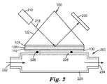
本開示によるSPRセンサー素子は、SPRセンサーにおいて有用である。ここで図2を参照すると、代表的なSPRセンサー200は、p偏光源210と、SPRセンサー素子100と、蒸気送達チャンバ220と、検出器230と、を備える。SPRセンサー素子100は、任意に、光の入射角を調節するために、回転台(図示せず)上に設置してもよい。
The SPR sensor element according to the present disclosure is useful in an SPR sensor. Referring now to FIG. 2, an
p偏光源210は、p偏光(すなわち、電場成分が入射光線及び金属薄層の面法線と同一平面で偏光する)である光を提供する。これは、レーザー又はコリメート白色光源などの光源を、偏光子及び任意の集光光学素子と組み合わせて用いることにより達成できる。結果として生じるSPR像に干渉縞を生じ得るため、一般的にレーザーよりもコリメート白色光源の使用が望ましい。偏光子は、p偏光を選択するために用いられ、任意の集光光学素子(白色光源と共に用いられる)は狭帯域フィルターからなり、典型的には、実験用の励起波長の選択に用いられる近赤外領域が中心にある。SPRセンサー素子100は、金属薄層上にp偏光が入射するように配置される。
The p-polarized
蒸気送達チャンバ220は、吸気口222と、排気口224と、サンプリング口226と、を備える。サンプリング口226及び吸収層130の少なくとも一部は、Oリング228を用いて共に密封されている。典型的な使用法では、分析される被検蒸気は、吸気口222を通って蒸気送達チャンバ220に導入される。蒸気送達チャンバ220は、例えば、金属、ガラス、又はプラスチックなどの任意の気体不透過性材料で作製されてもよい。
The
典型的には、被検蒸気は揮発性有機化合物を含むが、これは必須ではない。好適な被検蒸気の例として、脂肪族炭化水素(例えば、n−オクタン又はシクロヘキサン)、ケトン(例えば、アセトン又はメチルエチルケトン)、芳香族炭化水素(ベンゼン、トルエン、クロロベンゼン、又はナフタレン)、ニトリル(例えば、アセトニトリル又はベンゾニトリル)、塩素化脂肪族炭化水素(例えば、クロロホルム、ジクロロエタン、塩化メチレン、四塩化炭素、又はテトラクロロエチレン)、エステル5(esters 5)(例えば、酢酸ビニル、酢酸エチル、酢酸ブチル、又は安息香酸メチル)、硫化物(例えば、フェニルメルカプタン)、エーテル(例えば、メチルイソブチルエーテル又はジエチルエーテル)、アルデヒド(例えば、ホルムアルデヒド、ベンズアルデヒド、又はアセトアルデヒド)、アルコール(例えば、メタノール又はエタノール)、アミン(例えば、2−アミノピリジン)、有機酸(例えば、酢酸酸、プロパン酸)、イソシアネート(例えば、メチルイソシアネート又はトルエン−2,4−ジイソシアネート)、及びニトロ置換有機(例えば、ニトロメタン又はニトロベンゼン)が挙げられる。 Typically, the test vapor comprises a volatile organic compound, but this is not essential. Examples of suitable test vapors include aliphatic hydrocarbons (eg n-octane or cyclohexane), ketones (eg acetone or methyl ethyl ketone), aromatic hydrocarbons (benzene, toluene, chlorobenzene or naphthalene), nitriles (eg , Acetonitrile or benzonitrile), chlorinated aliphatic hydrocarbons (eg, chloroform, dichloroethane, methylene chloride, carbon tetrachloride, or tetrachloroethylene), esters 5 (eg, vinyl acetate, ethyl acetate, butyl acetate, or Methyl benzoate), sulfides (eg phenyl mercaptan), ethers (eg methyl isobutyl ether or diethyl ether), aldehydes (eg formaldehyde, benzaldehyde or acetaldehyde), alcohols (eg Ethanol or ethanol), amines (eg 2-aminopyridine), organic acids (eg acetic acid, propanoic acid), isocyanates (eg methyl isocyanate or toluene-2,4-diisocyanate), and nitro-substituted organics (eg Nitromethane or nitrobenzene).
検出器230は、金属薄層から反射される光の最低強度に対応する像を検出し、それによって共鳴角を測定する。吸収層に吸収される被検蒸気量に応じてその誘電率が変化し、その結果に対応して反射光の角度が変化する。検出器の応答は、蒸気送達チャンバ中の被検蒸気濃度に相関し得る。好適な検出器として、例えば、光電子増倍管、フォトダイオード、光導電体、フォトトランジスター、及び電荷結合検出器(CCD)が挙げられる。例えば、線状CCDアレイを使用してもよい。
The
所望の場合、センサー素子を高温(例えば、50℃〜70℃の範囲)に加熱してもよい。これにより、センサー素子の応答における湿度の影響を小さくできる。 If desired, the sensor element may be heated to an elevated temperature (eg, in the range of 50 ° C to 70 ° C). Thereby, the influence of humidity on the response of the sensor element can be reduced.
以下の非限定的な実施例によって本開示の目的及び利点を更に例示するが、これらの実施例に記載する特定の材料及びその量、並びに他の条件及び詳細は、本開示を不当に限定するものとして解釈されるべきではない。 The following non-limiting examples further illustrate the objects and advantages of the present disclosure, but the specific materials and amounts thereof described in these examples, as well as other conditions and details, unduly limit the present disclosure. It should not be interpreted as a thing.
特に断らないかぎり、実施例及び本明細書の残りの部分における全ての部、比率(%)及び比等は、重量基準である。 Unless otherwise noted, all parts, ratios (%), ratios, etc. in the examples and the rest of the specification are by weight.
PIM材料(PIM−1)の調製
モノマーである、5,5’,6,6’−テトラヒドロキシ−3,3,3’,3’−テトラメチル−1,1’−スピロビスインダン及びテトラフルオロテレフタロニトリルから、BuddらによってAdvanced Materials,2004,Vol.16,No.5,pp.456〜459に報告されている手順に概ね従って、PIM−1(固有ミクロ孔質のポリマー)を調製した。5,5’,6,6’−テトラヒドロキシ−3,3,3’,3’−テトラメチル−1,1’−スピロビスインダン(40.000グラム(g))を、23.724gのテトラフルオロテレフタロニトリル、97.373gの炭酸カリウム、及び1016.8gのN,N−ジメチルホルムアミドと混合し、この混合物を68℃で72時間加熱した。結果として生じる混合物を水中に注ぎ、沈殿を真空濾過により単離した。得られた材料をテトラヒドロフランに2回溶解し、メタノールから沈殿させ、室温で風乾した。乾燥したPIM−1ポリマーは、光散乱検出を利用するゲルろ過クロマトグラフィー分析によって測定するとき、約41,900グラム/モルの数平均分子量を有して得られた、固体の黄色生成物であった。
Preparation of PIM Material (PIM-1)
センサー素子用ガラススライドの作製
ガラススライド(Precision Glass & Optics(Santa Ana,California)のガラス番号0050−0050−0010−GF−CA、50mm×50mm、1.1mm厚、材料C−263、表面80/50)を、Alconox,Inc.(White Plains,New York)のALCONOX LIQUI−NOX洗剤溶液に30〜60分間浸漬して洗浄し、続いて毛ブラシでスライドの両面をこすり、温かい水道水ですすいだ後に、最後に脱イオン水ですすいだ。スライドは、表面への粉塵の堆積を防止するために風乾で遮蔽された。Entegris(Chaska,Minnesota)の3インチ(7.6cm)のウエファーキャリアに、乾燥した清潔なスライドを保管した。
Preparation of glass slide for sensor element Glass slide (Precision Glass & Optics (Santa Ana, California) glass number 0050-0050-0010-GF-CA, 50 mm × 50 mm, 1.1 mm thickness, material C-263,
表面プラズモン共鳴センサー
図2に概略が示されるように、表面プラズモン共鳴センサーを組み立てた。屈折率一致油(Cargille−Sacher Laboratories,Inc.(Cedar Grove,New Jersey)のシリーズA、25℃におけるnD=1.560±0.0002)を一滴用いて、プリズム(Edmund Optics(Barrington,New Jersey)のN−BK7未コーティングプリズム、在庫番号NT32−549)上にセンサー素子を装着した。SPRセンサー搭載プリズムを、Oリング、センサーホルダー、及びネジを用いて、VOC送達チャンバに装着した。単色放射源は、レーザー電源(Uniphaseのモデル1201−1)を備えたp偏光He−Neレーザー(632.8nm、Uniphase(Milpitas,California)から入手)とした。高輝度レーザー源が検出信号の飽和の原因となるため、フィルター(FSR−OD 300吸収性NDフィルター、直径25.4mm、546.1nmにおける3.0 OD、Newport Corp.(Irvine,California)から入手)をレーザーの前に設置した。センサーホルダーを回転せずに広範な角度で反射を得るために、レーザーとセンサー素子ホルダーとの間にレンズ(DIN 60、開口数=0.85、Edmund optics(Barrington,New Jersey)から入手)を置いた。最小反射位置を特定するために、電源(モデル6212A、Hewett Packard(Palo Alto,California)から入手)を備えた線状の128ピクセルCCDアレイ(モデルTSL1401R、TAOS(Plano,Texas)から入手)を用いた。このピクセルは、63.5マイクロメートル(高さ)×55.5マイクロメートル(幅)、中心間隔63.5マイクロメートル、ピクセル間隔8マイクロメートルである。CCDアレイの全長は、128ピクセルで0.813センチメートルであった。このCCDアレイを評価モジュール(モデルPC404A、TAOS(Plano,Texas)から入手)上に装着し、このモジュールを3方向移行台(Line Tool(Allentown,Pennsylvania)から入手)に取り付けた。金/ポリマー検知層とCCDアレイとの間の距離は2.25センチメートルであり、CCDアレイは反射された放射線に対して垂直の方向とした。ディジタルカメラを用いて装置構成の画像を撮影し、ディジタルカメラ像を解析することによって、入射光角を測定した。評価モジュールからの信号は、オシロスコープ(モデルTDS 3024B、Tektronix(Beaverton,Oregon)から入手)によって取得した。カスタマイズしたLabviewプログラムを用いて、データ収集用にTektronixオシロスコープに接続した。Labview(National Instruments(Austin,Texas)から入手可能なソフトウェア)プログラムに組み込まれた山/谷ファインダーアルゴリズムを用いて、最小反射位置を算出した。
Surface Plasmon Resonance Sensor A surface plasmon resonance sensor was assembled as outlined in FIG. Using a drop of refractive index matching oil (Cargille-Sacher Laboratories, Inc. (Cedar Grove, New Jersey), Series A, n D = 1.560 ± 0.0002 at 25 ° C.), a prism (Edmund Optics (Barrington, New York)). The sensor element was mounted on an N-BK7 uncoated prism from Jersey), stock number NT32-549). The SPR sensor mounted prism was attached to the VOC delivery chamber using an O-ring, sensor holder, and screws. The monochromatic radiation source was a p-polarized He-Ne laser (632.8 nm, obtained from Uniphase (Milpitas, Calif.)) Equipped with a laser power source (Uniphase model 1201-1). Obtained from filters (FSR-OD 300 absorbing ND filter, diameter 25.4 mm, 3.0 OD at 546.1 nm, Newport Corp. (Irvine, Calif.) As high-intensity laser sources cause detection signal saturation. ) Was installed in front of the laser. To obtain reflection at a wide range of angles without rotating the sensor holder, a lens (
全ての試験は、DRIERITE乾燥剤(W.A.Hammond Drierite Co.Ltd.(Xenia,Ohio))を通して水分を除去し、活性炭を通していかなる有機汚染物を除いた、空気中で行った。蒸気試験は、システムを通過する10L/分の乾燥空気流を用いて実施した。VOCレベルは、1ミリリットルのガスタイトシリンジ(Hamilton Company(Reno,Nevada)から入手)を装着したKD Scientificシリンジポンプ(KD Scientific Inc.(Holliston,Massachusetts)から入手可能)を用いて生成した。シリンジポンプによって、500mL容の三口フラスコに吊り下げた1片の濾紙上にVOC溶媒を送達した。乾燥空気流を濾紙に通し、溶媒を気化した。シリンジポンプを制御することによって様々な速度で溶媒を供給すると、様々な濃度の蒸気が発生した。シリンジポンプは、試験中にVOC特性の発生を可能にするLABVIEWプログラムによって制御した。MIRAN IR分析器(Thermo Fischer Scientific,Inc.(Waltham,Massachusetts))を用いて、設定濃度を確認した。全ての測定を室温で実施した。 All tests were performed in air, with moisture removed through a DRIERITE desiccant (WA Hammond Drierite Co. Ltd., Xenia, Ohio) and any organic contaminants removed through activated carbon. The steam test was performed using a 10 L / min dry air flow through the system. VOC levels were generated using a KD Scientific syringe pump (available from KD Scientific Inc., available from Holliston, Massachusetts) fitted with a 1 milliliter gas tight syringe (obtained from Hamilton Company (Reno, Nevada)). The VOC solvent was delivered by a syringe pump onto a piece of filter paper suspended in a 500 mL three-necked flask. A stream of dry air was passed through the filter paper to evaporate the solvent. When the solvent was supplied at different rates by controlling the syringe pump, different concentrations of vapor were generated. The syringe pump was controlled by a LABVIEW program that allowed generation of VOC characteristics during the test. The set concentration was confirmed using a MIRAN IR analyzer (Thermo Fischer Scientific, Inc. (Waltham, Massachusetts)). All measurements were performed at room temperature.
全てSigma−Aldrich(Milwaukee,Wisconsin)から入手した3種類の異なる溶媒、トルエン、エタノール及びメチルエチルケトン(MEK)を評価した。 All three different solvents, toluene, ethanol and methyl ethyl ketone (MEK), all obtained from Sigma-Aldrich (Milwaukee, Wisconsin) were evaluated.
(実施例1)
0.1nm/秒(nm/sec)の速度で金を熱蒸着することにより、30.0nm厚の金層を、清浄なガラススライド上にコーティングした。蒸着プロセスは、Inficon(East Syracuse,New York)のInficon XTC/2薄膜蒸着制御装置を用いて制御した。
Example 1
A 30.0 nm thick gold layer was coated on a clean glass slide by thermally depositing gold at a rate of 0.1 nm / second (nm / sec). The deposition process was controlled using an Inficon XTC / 2 thin film deposition controller from Inficon (East Syracuse, New York).
小容器中でPIM−1ポリマーをクロロベンゼンと合わせ、ローラーミル(Wheaton Science Products(Millville,New Jersey)のMini Bottle Roller番号348920)上で約4時間混合することにより、5.5重量パーセントのPIM溶液を調製した。次にこの溶液を、1マイクロメートルのフィルター(Pall Corp.(Port Washington,New York)の、1マイクロメートルのガラス繊維膜を付けたACRODISC 25mmシリンジフィルター)を通して濾過し、一晩放置して気泡を抜いた。 5.5 weight percent PIM solution by combining PIM-1 polymer with chlorobenzene in a small container and mixing on a roller mill (Mini Bottle Roller # 348892 from Wheaton Science Products (Millville, New Jersey)) for about 4 hours. Was prepared. The solution is then filtered through a 1 micrometer filter (Pall Corp. (Port Washington, New York) ACRODISC 25 mm syringe filter with 1 micrometer glass fiber membrane) and allowed to stand overnight for air bubbles. I pulled it out.
Laurell Technologies Corporation(North Wales,Pennsylvania)のModel WS 400B−8NPP/LITEスピンコーターを用いて、スライドの金面にPIM−1溶液をスピンコーティングした。PIM溶液を、300rpmで15秒間スライドに分注し、その後2000rpmで45秒間コーティングした。PIM層の厚さは620nmであった。アセトンに浸した綿棒でコーティングを少し除去し、Ambios Technology(Santa Cruz,California)のModel XP−1 Profilometerで計測することによって、厚さを測定した。測定で用いたパラメーターは、スキャン速度0.1mm/秒、スキャン長さ5mm、範囲10マイクロメートル、針圧0.20mg、及びフィルターレベル4であった。測定後、コーティングされたスライドを、100℃で1時間加熱乾燥した。 The gold surface of the slide was spin coated with a PIM-1 solution using a Model WS 400B-8NPP / LITE spin coater from Laurell Technologies Corporation (North Wales, Pennsylvania). The PIM solution was dispensed onto slides at 300 rpm for 15 seconds and then coated at 2000 rpm for 45 seconds. The thickness of the PIM layer was 620 nm. The coating was slightly removed with a cotton swab soaked in acetone, and the thickness was measured by measuring with a Model XP-1 Profilometer from Ambios Technology (Santa Cruz, California). The parameters used in the measurement were a scan speed of 0.1 mm / second, a scan length of 5 mm, a range of 10 micrometers, a needle pressure of 0.20 mg, and a filter level of 4. After the measurement, the coated slide was heat-dried at 100 ° C. for 1 hour.
標準的ガラス用カッターを用いて、コーティングされたスライドを4枚の25mm×25mmの素子に切り分けることによって、個々のセンサー素子を作製した。前側(使用する)表面を支持して損傷を防ぎながら、スライドの後側(使用しない面)を切断した。個々のセンサー素子に切り分けた後、Entegris(Chaska,Minnesota)の1.5インチ(3.8cm)のウエファーホルダーに、センサー素子を保管した。 Individual sensor elements were made by cutting the coated slides into four 25 mm x 25 mm elements using a standard glass cutter. The back side (the unused surface) of the slide was cut while supporting the front (used) surface to prevent damage. After being cut into individual sensor elements, the sensor elements were stored in a 1.5 inch (3.8 cm) wafer holder of Entegris (Chashka, Minnesota).
上記のように、センサー素子をSPRセンサー装置に装着した。乾燥空気下の入射光角は63.5度であった。一連のトルエン濃度(すなわち、乾燥空気中3、6、9、12ppmのトルエン)に、センサーを曝した。
As described above, the sensor element was attached to the SPR sensor device. The incident light angle under dry air was 63.5 degrees. The sensor was exposed to a series of toluene concentrations (
図3は、CCDアレイから得られた信号を報告している。大きいピクセル位置は、大きい角度で反射された放射線を示す。トルエン曝露がない場合(0ppmトルエン)、はっきりした最小反射(谷)が観察された。トルエンに曝露すると、最小反射の位置はより大きいピクセル位置にシフトした。 FIG. 3 reports the signal obtained from the CCD array. Large pixel locations indicate radiation reflected at large angles. In the absence of toluene exposure (0 ppm toluene), a clear minimum reflection (valley) was observed. Upon exposure to toluene, the position of minimum reflection shifted to a larger pixel position.
図4は、一連のトルエン曝露後の谷位置変化を、時間に対して記録している。各段階の濃度において、はっきりした谷位置変化段階が見られる。信号がある程度変動するのは、シリンジポンプに起因するトルエン蒸気の送達の変動による。変動によって、SPRセンサーの応答時間の見通しが与えられる。SPRセンサーは、自然発生的に変動するVOC濃度に対し、数秒で自然に応答できる。 FIG. 4 records the valley position change after a series of toluene exposures versus time. There is a clear valley position change step at each step concentration. Some variation in the signal is due to variations in toluene vapor delivery due to the syringe pump. The variation gives an overview of the response time of the SPR sensor. The SPR sensor can naturally respond to spontaneously changing VOC concentrations in seconds.
(実施例2)
スライド上に2種類の金属層をコーティングし、3.6固体重量パーセントのPIM−1溶液を用いた以外は、実施例1に記載する手順に従ってセンサー素子を作製した。5.0nm厚のチタン層を、0.1nm/秒の速度でPGOスライド上に堆積し、その後30.0nmの金層を0.5nm/秒の速度でチタン層上に堆積した。
(Example 2)
A sensor element was prepared according to the procedure described in Example 1 except that two metal layers were coated on the slide and a 3.6 solid weight percent PIM-1 solution was used. A 5.0 nm thick titanium layer was deposited on the PGO slide at a rate of 0.1 nm / sec, followed by a 30.0 nm gold layer deposited on the titanium layer at a rate of 0.5 nm / sec.
3.6重量パーセントのクロロベンゼン中PIM−1溶液(実施例1に概説されるように調製した)を、300rpmで15秒間センサーに分注し、続いて4000rpmで45秒間コーティングした。PIM−1層の厚さは203nmであった。乾燥空気下の放射角は51.5度であった。 A 3.6 weight percent PIM-1 solution in chlorobenzene (prepared as outlined in Example 1) was dispensed onto the sensor at 300 rpm for 15 seconds, followed by coating at 4000 rpm for 45 seconds. The thickness of the PIM-1 layer was 203 nm. The radiation angle under dry air was 51.5 degrees.
上記のように、センサー素子をSPRセンサー装置にそれぞれ装着した。エタノール、メチルエチルケトン(MEK)、又はトルエンを用いて、各センサー素子を試験した。結果を下記の表1、2及び3に示す。 As described above, each sensor element was attached to the SPR sensor device. Each sensor element was tested using ethanol, methyl ethyl ketone (MEK), or toluene. The results are shown in Tables 1, 2 and 3 below.
(比較例C1)
1.7パーセントのクロロホルム中ポリカーボネート(MAKROLONポリカーボネートに相当するSigma Aldrich(Milwaukee,Wisconsin)のポリ(ビスフェノールAカーボネート)ポリカーボネート、更なる精製は行わずに使用した)溶液を、300rpmで5秒間スライドに分注し、その後3000rpmで40秒間コーティングした以外は、実施例2の手順に従ってセンサーを作製した。ポリカーボネート層の厚さは221nmであった。実施例2に記載のように、エタノール、MEK、及びトルエンを用いてセンサー素子を試験した。乾燥空気下の放射角は61.5度であった。結果を下記の表1、2及び3に報告される。
(Comparative Example C1)
A solution of 1.7 percent polycarbonate in chloroform (Sigma Aldrich (Milwaukee, Wisconsin) poly (bisphenol A carbonate) polycarbonate equivalent to MAKROLON polycarbonate, used without further purification) was dispensed on a slide at 300 rpm for 5 seconds. A sensor was made according to the procedure of Example 2 except that it was then coated at 3000 rpm for 40 seconds. The thickness of the polycarbonate layer was 221 nm. The sensor element was tested using ethanol, MEK, and toluene as described in Example 2. The radiation angle under dry air was 61.5 degrees. The results are reported in Tables 1, 2 and 3 below.
[本開示の選択された実施形態]
第1の実施形態では、本開示は、
金属薄層と、
光を金属薄層の方へ、及び金属薄層から離れる方へ方向付けるための、金属薄層上に配置される光学構造物と、
金属薄層上に光学構造物とは反対側に配置される吸収層であって、少なくとも0.4立法ナノメートルである平均細孔容積を有する固有ミクロ孔質のポリマーを含む吸収層と、を備える、表面プラズモン共鳴センサー素子を提供する。
[Selected Embodiments of the Present Disclosure]
In the first embodiment, the present disclosure provides:
A thin metal layer,
An optical structure disposed on the thin metal layer for directing light toward the thin metal layer and away from the thin metal layer;
An absorbing layer disposed on a thin metal layer opposite the optical structure, the absorbing layer comprising an intrinsic microporous polymer having an average pore volume that is at least 0.4 cubic nanometers; A surface plasmon resonance sensor element is provided.
第2の実施形態では、本開示は、光学構造物がプリズムからなる、第1の実施形態に記載の表面プラズモン共鳴センサー素子を提供する。 In a second embodiment, the present disclosure provides the surface plasmon resonance sensor element according to the first embodiment, wherein the optical structure is a prism.
第3の実施形態では、本開示は、光学構造物が、プリズムと、透明プレートと、それらの間に挟まれる流体と、を含み、プリズム、透明プレート、及び流体が一致した屈折率を有する、第1又は第2の実施形態に記載の表面プラズモン共鳴センサー素子を提供する。 In a third embodiment, the present disclosure provides that the optical structure includes a prism, a transparent plate, and a fluid sandwiched therebetween, and the prism, the transparent plate, and the fluid have a matching refractive index. The surface plasmon resonance sensor element described in the first or second embodiment is provided.
第4の実施形態では、本開示は、固有ミクロ孔質のポリマーが、少なくとも0.45立法ナノメートルである平均細孔容積を有する、第1〜第3の実施形態のいずれか1つに記載の表面プラズモン共鳴センサー素子を提供する。 In a fourth embodiment, the present disclosure describes in any one of the first to third embodiments, wherein the intrinsic microporous polymer has an average pore volume that is at least 0.45 cubic nanometers. A surface plasmon resonance sensor element is provided.
第5の実施形態では、本開示は、固有ミクロ孔質のポリマーが、以下からなる群から選択されるモノマー単位を有するホモポリマーである、第1〜第4の実施形態のいずれか1つに記載の表面プラズモン共鳴センサー素子を提供する。 In a fifth embodiment, the disclosure relates to any one of the first to fourth embodiments, wherein the intrinsic microporous polymer is a homopolymer having monomer units selected from the group consisting of: A surface plasmon resonance sensor element as described is provided.
第6の実施形態では、本開示は、金属薄層が、金、銀、アルミニウム、又は銅のうち少なくとも1つを含む、第1〜第5の実施形態のいずれか1つに記載の表面プラズモン共鳴センサー素子を提供する。 In a sixth embodiment, the present disclosure provides the surface plasmon according to any one of the first to fifth embodiments, wherein the thin metal layer includes at least one of gold, silver, aluminum, or copper. A resonant sensor element is provided.
第7の実施形態では、本開示は、
p偏光源と、
第1〜第7の実施形態のいずれか1つに記載の表面プラズモン共鳴センサー素子と、
金属薄層から反射される光の最低強度に対応する像を検出し、それによって共鳴角を測定するための検出器と、を備える、表面プラズモン共鳴センサーを提供する。
In the seventh embodiment, the present disclosure provides:
a p-polarization source;
The surface plasmon resonance sensor element according to any one of the first to seventh embodiments;
A surface plasmon resonance sensor comprising: a detector for detecting an image corresponding to a minimum intensity of light reflected from a thin metal layer, and thereby measuring a resonance angle.
第8の実施形態では、本開示は、p偏光源がレーザーを含む、第7の実施形態に記載の表面プラズモン共鳴センサーを提供する。 In an eighth embodiment, the present disclosure provides the surface plasmon resonance sensor according to the seventh embodiment, wherein the p-polarized source includes a laser.
第9の実施形態では、本開示は、検出器がフォトダイオードアレイを備える、第7又は第8の実施形態に記載の表面プラズモン共鳴センサーを提供する。 In a ninth embodiment, the present disclosure provides the surface plasmon resonance sensor according to the seventh or eighth embodiment, wherein the detector comprises a photodiode array.
第10の実施形態では、本開示は、光学構造物がプリズムからなる、第7〜第9の実施形態のいずれか1つに記載の表面プラズモン共鳴センサーを提供する。 In the tenth embodiment, the present disclosure provides the surface plasmon resonance sensor according to any one of the seventh to ninth embodiments, in which the optical structure includes a prism.
第11の実施形態では、本開示は、光学構造物が、プリズムと、透明プレートと、それらの間に挟まれる流体と、を含み、プリズム、透明プレート、及び流体が一致した屈折率を有する、第7〜第9の実施形態のいずれか1つに記載の表面プラズモン共鳴センサーを提供する。 In an eleventh embodiment, the present disclosure provides that the optical structure includes a prism, a transparent plate, and a fluid sandwiched therebetween, and the prism, the transparent plate, and the fluid have a matching refractive index. A surface plasmon resonance sensor according to any one of the seventh to ninth embodiments is provided.
当業者であれば、本開示の範囲及び趣旨から逸脱することなく本開示の様々な改変及び変更を行うことが可能であり、また、本開示は上記に記載した例示的な実施形態に不要に限定されるべきではない点は理解されるべきである。 Those skilled in the art can make various modifications and changes to the present disclosure without departing from the scope and spirit of the present disclosure, and the present disclosure is unnecessary for the exemplary embodiments described above. It should be understood that it should not be limited.
Claims (2)
光を前記金属薄層の方へ、及び前記金属薄層から離れる方へ方向付けるための、前記金属薄層上に配置される光学構造物と、
前記金属薄層上に前記光学構造物とは反対側に配置される吸収層であって、少なくとも0.4立方ナノメートルである平均細孔容積を有する固有ミクロ孔質のポリマーを備える吸収層と、を備える、表面プラズモン共鳴センサー素子。 A thin metal layer,
An optical structure disposed on the thin metal layer for directing light toward the thin metal layer and away from the thin metal layer;
An absorbent layer disposed on the thin metal layer opposite the optical structure, the absorbent layer comprising an intrinsic microporous polymer having an average pore volume of at least 0.4 cubic nanometers; A surface plasmon resonance sensor element.
請求項1に記載の表面プラズモン共鳴センサー素子と、
金属薄層から反射される光の最低強度に対応する像を検出し、それによって共鳴角を測定するための検出器と、を備える、表面プラズモン共鳴センサー。 a p-polarization source;
A surface plasmon resonance sensor element according to claim 1;
A surface plasmon resonance sensor comprising: a detector for detecting an image corresponding to a minimum intensity of light reflected from the thin metal layer and thereby measuring a resonance angle.
Applications Claiming Priority (3)
| Application Number | Priority Date | Filing Date | Title |
|---|---|---|---|
| US201161497632P | 2011-06-16 | 2011-06-16 | |
| US61/497,632 | 2011-06-16 | ||
| PCT/US2012/042233 WO2012174099A1 (en) | 2011-06-16 | 2012-06-13 | Surface plasmon resonance sensor element and sensor including the same |
Publications (3)
| Publication Number | Publication Date |
|---|---|
| JP2014517321A JP2014517321A (en) | 2014-07-17 |
| JP2014517321A5 JP2014517321A5 (en) | 2015-07-30 |
| JP6061920B2 true JP6061920B2 (en) | 2017-01-18 |
Family
ID=46354481
Family Applications (1)
| Application Number | Title | Priority Date | Filing Date |
|---|---|---|---|
| JP2014515957A Expired - Fee Related JP6061920B2 (en) | 2011-06-16 | 2012-06-13 | Surface plasmon resonance sensor element and sensor including the same |
Country Status (6)
| Country | Link |
|---|---|
| US (1) | US9244008B2 (en) |
| EP (1) | EP2721393B1 (en) |
| JP (1) | JP6061920B2 (en) |
| KR (1) | KR101875174B1 (en) |
| CN (1) | CN103620387B (en) |
| WO (1) | WO2012174099A1 (en) |
Families Citing this family (12)
| Publication number | Priority date | Publication date | Assignee | Title |
|---|---|---|---|---|
| EP2697637B1 (en) | 2011-04-13 | 2021-01-13 | 3M Innovative Properties Company | Vapor sensor including sensor element with integral heating |
| CN103492872B (en) | 2011-04-13 | 2016-04-06 | 3M创新有限公司 | Use the method for absorbability sensor element |
| JP5955379B2 (en) | 2011-04-13 | 2016-07-20 | スリーエム イノベイティブ プロパティズ カンパニー | Method for detecting volatile organic compounds |
| CN104024848B (en) | 2011-12-13 | 2016-01-20 | 3M创新有限公司 | For identifying the method with the unknown organic compound in quantitative measurement gas medium |
| JP6483668B2 (en) | 2013-09-26 | 2019-03-13 | スリーエム イノベイティブ プロパティズ カンパニー | Vapor sensor suitable for detecting residual alcohol in skin areas |
| US10281397B2 (en) * | 2015-11-10 | 2019-05-07 | Schlumberger Technology Corporation | Optical sensors using surface plasmon resonance to determine at least one property relating to phase change of a hydrocarbon-based analyte |
| US10254216B2 (en) * | 2016-06-30 | 2019-04-09 | Schlumberger Technology Corporation | Systems, methods and apparatus for analysis of reservoir fluids using surface plasmon resonance |
| SG11202008686TA (en) | 2018-03-08 | 2020-10-29 | Exxonmobil Res & Eng Co | Spirocentric compounds and polymers thereof |
| WO2019231869A1 (en) * | 2018-05-27 | 2019-12-05 | Biosensing Instrument Inc. | Surface plasmon resonance imaging system and method for measuring molecular interactions |
| US11231365B2 (en) * | 2019-07-08 | 2022-01-25 | Hanwha Systems Co., Ltd. | Apparatus and method for infrared imaging |
| WO2021124046A1 (en) * | 2019-12-20 | 2021-06-24 | 3M Innovative Properties Company | Nanohole array sensor elements and sensors including the same |
| WO2022234533A1 (en) * | 2021-05-06 | 2022-11-10 | 3M Innovative Properties Company | Metallic nanohole array on nanowell sensing element |
Family Cites Families (23)
| Publication number | Priority date | Publication date | Assignee | Title |
|---|---|---|---|---|
| JPH06281610A (en) | 1993-01-29 | 1994-10-07 | Nok Corp | Humidity sensor, alcohol sensor or ketone sensor |
| JPH08193948A (en) | 1995-01-18 | 1996-07-30 | Toto Ltd | Exciting structure for surface plasmon resonance phenomenon and biosensor |
| ATE466275T1 (en) * | 2000-03-14 | 2010-05-15 | Spring Systems Ab | SPR DEVICE WITH IMPROVED IMAGE |
| US7193711B2 (en) * | 2000-07-11 | 2007-03-20 | Maven Technologies, Llc | Imaging method and apparatus |
| US6778316B2 (en) * | 2001-10-24 | 2004-08-17 | William Marsh Rice University | Nanoparticle-based all-optical sensors |
| US7449146B2 (en) | 2002-09-30 | 2008-11-11 | 3M Innovative Properties Company | Colorimetric sensor |
| GB0317557D0 (en) | 2003-07-26 | 2003-08-27 | Univ Manchester | Microporous polymer material |
| US20050265648A1 (en) * | 2004-06-01 | 2005-12-01 | Daniel Roitman | Evanescent wave sensor containing nanostructures and methods of using the same |
| KR100723401B1 (en) * | 2005-01-29 | 2007-05-30 | 삼성전자주식회사 | Long-range SPR device having nanoporous material and method for fabricating the same |
| FR2890745B1 (en) * | 2005-09-15 | 2007-11-30 | Commissariat Energie Atomique | NANOPOROUS MATERIAL OF ALDEHYDES WITH DIRECT OPTICAL TRANSDUCTION |
| US7556774B2 (en) | 2005-12-21 | 2009-07-07 | 3M Innovative Properties Company | Optochemical sensor and method of making the same |
| US7767143B2 (en) | 2006-06-27 | 2010-08-03 | 3M Innovative Properties Company | Colorimetric sensors |
| US7715002B2 (en) * | 2007-01-23 | 2010-05-11 | Bionorica Ag | Method for classifying scientific materials such as silicate materials, polymer materials and/or nanomaterials |
| JP5266326B2 (en) | 2007-10-05 | 2013-08-21 | スリーエム イノベイティブ プロパティズ カンパニー | Organic chemical sensors including plasma deposited microporous layers, and methods of making and using the same |
| CN101815936B (en) * | 2007-10-05 | 2017-03-22 | 3M创新有限公司 | Organic chemical sensor comprising microporous polymer, and method of use |
| KR101702560B1 (en) | 2008-12-18 | 2017-02-13 | 삼성전자 주식회사 | Apparatus and method of detecting surface plasmon resonance |
| BRPI0918200A2 (en) | 2008-12-23 | 2015-12-08 | 3M Innovative Properties Co | detection element and method of detection of organic chemical analytes |
| KR200474377Y1 (en) | 2009-01-29 | 2014-09-12 | 쓰리엠 이노베이티브 프로퍼티즈 컴파니 | Monitor for Optical Detection of Organic Analytes |
| JP5369755B2 (en) * | 2009-02-25 | 2013-12-18 | 株式会社豊田中央研究所 | Gas sensor |
| CN102439422B (en) | 2009-03-30 | 2016-05-18 | 3M创新有限公司 | For detection of photoelectric method and the device of analyte |
| JP5460113B2 (en) * | 2009-04-23 | 2014-04-02 | 地方独立行政法人東京都立産業技術研究センター | Localized surface plasmon resonance measurement substrate and localized surface plasmon resonance sensor |
| GB0919742D0 (en) * | 2009-11-11 | 2009-12-30 | Millipore Corp | Optical sensor |
| JP5932806B2 (en) | 2010-09-30 | 2016-06-08 | スリーエム イノベイティブ プロパティズ カンパニー | SENSOR ELEMENT, MANUFACTURING METHOD THEREOF, AND SENSOR DEVICE INCLUDING THE SAME |
-
2012
- 2012-06-13 WO PCT/US2012/042233 patent/WO2012174099A1/en active Application Filing
- 2012-06-13 US US14/124,835 patent/US9244008B2/en active Active
- 2012-06-13 KR KR1020147000831A patent/KR101875174B1/en active IP Right Grant
- 2012-06-13 EP EP12729782.8A patent/EP2721393B1/en not_active Not-in-force
- 2012-06-13 CN CN201280029296.9A patent/CN103620387B/en not_active Expired - Fee Related
- 2012-06-13 JP JP2014515957A patent/JP6061920B2/en not_active Expired - Fee Related
Also Published As
| Publication number | Publication date |
|---|---|
| US20140111809A1 (en) | 2014-04-24 |
| WO2012174099A1 (en) | 2012-12-20 |
| CN103620387B (en) | 2017-02-15 |
| EP2721393A1 (en) | 2014-04-23 |
| EP2721393B1 (en) | 2018-02-28 |
| JP2014517321A (en) | 2014-07-17 |
| US9244008B2 (en) | 2016-01-26 |
| KR101875174B1 (en) | 2018-07-06 |
| CN103620387A (en) | 2014-03-05 |
| KR20140040220A (en) | 2014-04-02 |
Similar Documents
| Publication | Publication Date | Title |
|---|---|---|
| JP6061920B2 (en) | Surface plasmon resonance sensor element and sensor including the same | |
| JP6038950B2 (en) | Method for identification and quantitative measurement of unknown organic compounds in gaseous media | |
| US9429537B2 (en) | Method of detecting volatile organic compounds | |
| JP5968421B2 (en) | Usage of Absorbent Sensor Element | |
| EP2423668B1 (en) | System and method for detection of an analyte in a gaseous sample | |
| Nguyen et al. | A spectroscopic technique for in situ measurement of water at the coating/metal interface | |
| US20140302612A1 (en) | Nematic liquid crystal thin films for chemical vapor sensing | |
| US20150355156A1 (en) | Methods and apparatus for detecting metals in liquids | |
| JP5369755B2 (en) | Gas sensor | |
| Şen et al. | A macrocyclic tetra-undecyl calix [4] resorcinarene thin film receptor for chemical vapour sensor applications | |
| US8932880B2 (en) | Method for the direct measure of molecular interactions by detection of light reflected from multilayered functionalized dielectrics | |
| Martínez-Pérez et al. | Commercial polycarbonate track-etched membranes as substrates for low-cost optical sensors | |
| JPH05332937A (en) | Optical ion sensor | |
| Mutschler et al. | Characterization of thin polymer and biopolymer layers by ellipsometry and evanescent field technology | |
| Mehan et al. | Surface plasmon resonance based refractive index sensor for liquids | |
| US20230026261A1 (en) | Nanohole array sensor elements and sensors including the same | |
| FR2993987A1 (en) | OPTICAL METHODS FOR OBSERVING SAMPLES AND DETECTION OR DETERMINATION OF CHEMICAL OR BIOLOGICAL SPECIES. | |
| JP2011106928A (en) | Sensor and apparatus for detecting hydrogen adsorption | |
| JPS63281029A (en) | Detector | |
| US20110064616A1 (en) | Transport detector for liquid chromatography | |
| UA123357C2 (en) | APPARATUS FOR ANALYSIS OF LIQUID AND GAS MEDIUM MEDIA | |
| UA115610C2 (en) | A TENSION DEVICE FOR ANALYSIS OF BIOCCHEMICAL ENVIRONMENTS | |
| JP2007327833A (en) | Instrument for measuring surface plasmon resonance, and surface plasmon resonance measuring method | |
| UA76774U (en) | Device for analysis of biochemical media | |
| UA46512A (en) | SURFACE PLASMON RESONANCE DETECTOR |
Legal Events
| Date | Code | Title | Description |
|---|---|---|---|
| A521 | Request for written amendment filed |
Free format text: JAPANESE INTERMEDIATE CODE: A523 Effective date: 20150612 |
|
| A621 | Written request for application examination |
Free format text: JAPANESE INTERMEDIATE CODE: A621 Effective date: 20150612 |
|
| A131 | Notification of reasons for refusal |
Free format text: JAPANESE INTERMEDIATE CODE: A131 Effective date: 20160315 |
|
| A977 | Report on retrieval |
Free format text: JAPANESE INTERMEDIATE CODE: A971007 Effective date: 20160316 |
|
| A521 | Request for written amendment filed |
Free format text: JAPANESE INTERMEDIATE CODE: A523 Effective date: 20160615 |
|
| TRDD | Decision of grant or rejection written | ||
| A01 | Written decision to grant a patent or to grant a registration (utility model) |
Free format text: JAPANESE INTERMEDIATE CODE: A01 Effective date: 20161115 |
|
| A61 | First payment of annual fees (during grant procedure) |
Free format text: JAPANESE INTERMEDIATE CODE: A61 Effective date: 20161213 |
|
| R150 | Certificate of patent or registration of utility model |
Ref document number: 6061920 Country of ref document: JP Free format text: JAPANESE INTERMEDIATE CODE: R150 |
|
| LAPS | Cancellation because of no payment of annual fees |