JP6061505B2 - Optical scanning apparatus and image forming apparatus having the same - Google Patents
Optical scanning apparatus and image forming apparatus having the same Download PDFInfo
- Publication number
- JP6061505B2 JP6061505B2 JP2012131291A JP2012131291A JP6061505B2 JP 6061505 B2 JP6061505 B2 JP 6061505B2 JP 2012131291 A JP2012131291 A JP 2012131291A JP 2012131291 A JP2012131291 A JP 2012131291A JP 6061505 B2 JP6061505 B2 JP 6061505B2
- Authority
- JP
- Japan
- Prior art keywords
- light
- emitting element
- light emission
- light emitting
- emission intensity
- Prior art date
- Legal status (The legal status is an assumption and is not a legal conclusion. Google has not performed a legal analysis and makes no representation as to the accuracy of the status listed.)
- Active
Links
Images


Classifications
-
- G—PHYSICS
- G03—PHOTOGRAPHY; CINEMATOGRAPHY; ANALOGOUS TECHNIQUES USING WAVES OTHER THAN OPTICAL WAVES; ELECTROGRAPHY; HOLOGRAPHY
- G03G—ELECTROGRAPHY; ELECTROPHOTOGRAPHY; MAGNETOGRAPHY
- G03G15/00—Apparatus for electrographic processes using a charge pattern
- G03G15/04—Apparatus for electrographic processes using a charge pattern for exposing, i.e. imagewise exposure by optically projecting the original image on a photoconductive recording material
- G03G15/043—Apparatus for electrographic processes using a charge pattern for exposing, i.e. imagewise exposure by optically projecting the original image on a photoconductive recording material with means for controlling illumination or exposure
-
- G—PHYSICS
- G02—OPTICS
- G02B—OPTICAL ELEMENTS, SYSTEMS OR APPARATUS
- G02B26/00—Optical devices or arrangements for the control of light using movable or deformable optical elements
- G02B26/08—Optical devices or arrangements for the control of light using movable or deformable optical elements for controlling the direction of light
- G02B26/10—Scanning systems
- G02B26/12—Scanning systems using multifaceted mirrors
- G02B26/127—Adaptive control of the scanning light beam, e.g. using the feedback from one or more detectors
-
- G—PHYSICS
- G03—PHOTOGRAPHY; CINEMATOGRAPHY; ANALOGOUS TECHNIQUES USING WAVES OTHER THAN OPTICAL WAVES; ELECTROGRAPHY; HOLOGRAPHY
- G03G—ELECTROGRAPHY; ELECTROPHOTOGRAPHY; MAGNETOGRAPHY
- G03G15/00—Apparatus for electrographic processes using a charge pattern
- G03G15/04—Apparatus for electrographic processes using a charge pattern for exposing, i.e. imagewise exposure by optically projecting the original image on a photoconductive recording material
- G03G15/04036—Details of illuminating systems, e.g. lamps, reflectors
- G03G15/04045—Details of illuminating systems, e.g. lamps, reflectors for exposing image information provided otherwise than by directly projecting the original image onto the photoconductive recording material, e.g. digital copiers
- G03G15/04072—Details of illuminating systems, e.g. lamps, reflectors for exposing image information provided otherwise than by directly projecting the original image onto the photoconductive recording material, e.g. digital copiers by laser
Description
本発明は、光学走査装置、及び、それを有するレーザープリンタ、複写機、ファクシミリ等の電子写真記録方式を利用する画像形成装置に関するものである。 The present invention relates to an optical scanning apparatus and an image forming apparatus using an electrophotographic recording system such as a laser printer, a copying machine, and a facsimile machine having the optical scanning apparatus.
従来から、カラー画像形成装置において、異なる色で隣接して形成された画像の間に、本来あるべきでない白い隙間が空いてしまう、所謂ホワイトギャップという現象が知られている。この現象は、感光ドラム上に、ドラム表面電位が急峻に変化する静電潜像、例えば画像エッジ部が形成され、この部位を現像装置で現像した際、本来よりも顕画像が細く形成されることから発生する。例えばシアン色の帯とブラック色の帯を隣接させた画像において、本来であればシアン色の帯とブラック色の帯が隣接するはずが、夫々の顕画像が夫々細く形成されてしまい、記録材上の最終画像においてシアン色とブラック色との間に隙間ができてしまう。 2. Description of the Related Art Conventionally, in a color image forming apparatus, a so-called white gap phenomenon is known in which a white gap that should not originally exist is formed between images formed adjacent to each other in different colors. This phenomenon is that an electrostatic latent image, for example, an image edge portion, in which the drum surface potential changes sharply is formed on the photosensitive drum, and when this portion is developed by the developing device, a visible image is formed thinner than the original. It arises from that. For example, in an image in which a cyan band and a black band are adjacent to each other, a cyan band and a black band are supposed to be adjacent to each other. In the final image above, there will be a gap between cyan and black.
図17は、従来技術に係るホワイトギャップの詳細を説明する図であり、現像ローラと感光ドラムとの間の電界の様子を示す。ホワイトギャップの原因となる顕画部の顕画像の細りは、感光ドラム上に形成された静電部の静電潜像のエッジ部にて電界が巻き込んでしまうことに起因する。 FIG. 17 is a diagram for explaining the details of the white gap according to the prior art, and shows the state of the electric field between the developing roller and the photosensitive drum. The thinning of the visible image in the visible image area that causes the white gap is caused by the electric field being caught at the edge of the electrostatic latent image of the electrostatic area formed on the photosensitive drum.
この課題に対しては、印字可能領域全面における非画像部(非トナー像形成部)に、レーザースキャナの発光素子をトナー付着を起こさない程度に微少発光して、画像の細りを防止する方法が知られている。以下、この方法のことをバックグランド露光、或いは非画像部微少発光等と称する。 To solve this problem, there is a method for preventing the image from being thinned by causing the light emitting element of the laser scanner to emit a small amount of light to the non-image portion (non-toner image forming portion) in the entire printable area so as not to cause toner adhesion. Are known. Hereinafter, this method is referred to as background exposure or non-image portion minute light emission.
尚、非画像部微少発光を行う目的としては、ホワイトギャップの防止に限定されることはない。例えば、特許文献1に開示されるよう、転写電位コントラストを小さくし、転写ニップ部で発生する気中放電に伴う画像乱れの防止対策としても実施される。すなわち、非画像部微少発光は、特定の用途に限定されるものではない。
It should be noted that the purpose of performing non-image portion minute light emission is not limited to prevention of white gap. For example, as disclosed in
ここで非画像部微少発光の具体的手法として、例えばPWM(Pulse WidthModulation)方式と呼ばれる、パルス波のデューティー比を変化させる方法が特許文献1において提案されている。これは、固定周波数である画像用クロックに同期して、微少発光量に相当するパルス幅で非画像部においてレーザースキャナの発光素子を発光するものである。
Here, as a specific method of non-image portion minute light emission, for example, a method of changing a duty ratio of a pulse wave called a PWM (Pulse Width Modulation) method is proposed in
近年、カラー画像形成装置においては、益々の高画質化が要望されている。そのような中、発光素子に関して、画像部に対応する発光の発光強度の調整に加え、上で説明した非画像部の微少発光の発光強度を適切に調整することが課題となってくる。つまり、1つの発光素子が2つの発光強度で発光できるよう適切に調整することが課題となってくる。 In recent years, there has been a demand for higher image quality in color image forming apparatuses. Under such circumstances, regarding the light emitting element, in addition to the adjustment of the light emission intensity corresponding to the image portion, it is necessary to appropriately adjust the light emission intensity of the minute light emission of the non-image portion described above. That is, it is a problem to appropriately adjust so that one light emitting element can emit light with two light emission intensities.
本発明は、上記要望を鑑みてなされたものであり、1つの発光素子が2つの発光強度で発光するよう適切に調整することを目的とする。 The present invention has been made in view of the above-described demand, and an object thereof is to appropriately adjust so that one light emitting element emits light with two light emission intensities.
上記目的を達成するため、本発明は、レーザー光を発する発光素子と、駆動電流によって前記発光素子を駆動させる駆動手段と、所定速度で回転することで前記レーザー光を被走査面上で走査させる回転多面鏡と、前記発光素子から発せられ、前記回転多面鏡で反射したレーザー光を受光する受光手段と、前記回転多面鏡を駆動する回転多面鏡駆動手段と、前記回転多面鏡駆動手段の回転速度を制御する制御手段と、を有し、前記駆動手段は、第1発光強度及び前記第1発光強度よりも低い第2発光強度で前記発光素子を発光させることが可能な光学走査装置であって、前記駆動手段は、第1駆動電流に第2駆動電流を加えた駆動電流によって前記発光素子を感光体のトナーが付着する画像部に向かって前記第1発光強度で発光させ、且つ、前記第2駆動電流によって前記発光素子を感光体のトナーが付着しない非画像部に向かって前記第2発光強度で発光させ、前記駆動手段は、前記発光素子を前記第1発光強度で発光させて前記第1駆動電流を調整する第1調整工程と、前記発光素子を前記第2発光強度で発光させて前記第2駆動電流を調整する第2調整工程を実行可能で、前記駆動手段は、前記回転多面鏡が回転を開始してから前記所定速度となるまでの間で、前記第1調整工程及び前記第2調整工程を行い、前記回転多面鏡が回転を開始した後で且つ前記第1調整工程を行う前に、前記第2調整工程を行い、前記制御手段は、前記第2調整工程が行われている場合は、前記受光手段によるレーザー光の受光が行われているか否かに関わらず前記回転多面鏡駆動手段の回転速度を制御し、前記第1調整工程が行われている場合は、前記受光手段による受光結果に応じて前記回転多面鏡駆動手段の回転速度を制御することを特徴とする。 In order to achieve the above object, the present invention scans a laser beam on a surface to be scanned by rotating a light emitting element that emits laser light, a driving unit that drives the light emitting element by a driving current, and a predetermined speed. Rotating polygon mirror, light receiving means for receiving laser light emitted from the light emitting element and reflected by the rotating polygon mirror, rotating polygon mirror driving means for driving the rotating polygon mirror, and rotation of the rotating polygon mirror driving means Control means for controlling the speed, and the driving means is an optical scanning device capable of causing the light emitting element to emit light with a first light emission intensity and a second light emission intensity lower than the first light emission intensity. The driving means causes the light emitting element to emit light at the first light emission intensity toward the image portion on which the toner of the photoconductor adheres by a driving current obtained by adding the second driving current to the first driving current, and The second driving current causes the light emitting element to emit light at the second light emission intensity toward the non-image portion where the toner of the photoreceptor does not adhere, and the driving unit causes the light emitting element to emit light at the first light emission intensity. A first adjustment step of adjusting the first drive current; and a second adjustment step of adjusting the second drive current by causing the light emitting element to emit light at the second emission intensity. The first adjustment step and the second adjustment step are performed during the period from when the rotary polygon mirror starts to rotate until the predetermined speed is reached, and after the rotary polygon mirror starts rotating and the first adjustment before performing the process, have the rows of the second adjustment step, wherein, when the second adjusting process is being performed, whether or receiving the laser beam is being performed by said light receiving means The rotational speed of the rotary polygon mirror drive means Controls, when the first adjustment step is being performed, and controlling the rotational speed of the rotary polygon mirror drive unit according to the light receiving result by the light receiving means.
本発明によれば、1つの発光素子が2つの発光強度で発光するよう適切に調整することが可能となる。 According to the present invention, it is possible to appropriately adjust so that one light emitting element emits light with two light emission intensities.
<実施例1>
以下に、図面を参照して、この発明の好適な実施の形態を例示的に詳しく説明する。ただし、この実施の形態に記載されている構成要素はあくまで例示であり、この発明の範囲をそれらのみに限定する趣旨のものではない。
<Example 1>
Hereinafter, exemplary embodiments of the present invention will be described in detail with reference to the drawings. However, the constituent elements described in this embodiment are merely examples, and are not intended to limit the scope of the present invention only to them.
[画像形成装置]
図1は、カラー画像形成装置の概略断面図である。尚、以下の説明においては、カラー画像形成装置を用いて説明を行うが、それに限定されるものではない。後述にて詳しく説明する非画像部の微少発光については、例えば、単色の画像形成装置にも適用することが出来る。また、以下においては、インライン方式のカラー画像形成装置を例に説明を行うが、例えばロータリー方式のカラー画像形成装置でも良い。以下、インライン方式のカラー画像形成装置を例に詳述する。
[Image forming apparatus]
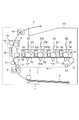
FIG. 1 is a schematic sectional view of a color image forming apparatus. In the following description, a color image forming apparatus is used for description, but the present invention is not limited to this. The minute light emission of the non-image portion, which will be described in detail later, can be applied to, for example, a monochrome image forming apparatus. In the following description, an inline type color image forming apparatus will be described as an example. However, for example, a rotary type color image forming apparatus may be used. Hereinafter, an inline type color image forming apparatus will be described in detail as an example.
図1に示す如く、カラーレーザープリンタ50は、複数の第1の像担持体である感光ドラム5(5Y,5M,5C,5K)を有し、順次、第2の像担持体である中間転写ベルト3に連続的に多重転写し、フルカラープリント画像を得るプリンタである。この方式をインライン方式或いは4連ドラム方式という。
As shown in FIG. 1, the
光学走査装置(レーザースキャナ)9(9Y,9M,9C,9K)はそれぞれ対応する感光ドラム5に光を照射して、感光ドラム5を露光する。
Optical scanning devices (laser scanners) 9 (9Y, 9M, 9C, 9K) irradiate the corresponding
中間転写ベルト3は、無端状のエンドレスベルトであり、駆動ローラ12、テンションローラ13、アイドラローラ17、および二次転写対向ローラ18に懸架され、図中矢印の方向にプロセススピード115mm/secで回転している。駆動ローラ12、テンションローラ13、および二次転写対向ローラ18は、中間転写ベルト3を支持する支持ローラであり、駆動ローラ12、二次転写対向ローラ18はφ24、テンションローラ13はφ16の構成となっている。
The
感光ドラム5(5Y,5M,5C,5K)は、中間転写ベルト3の移動方向に、直列に4本配置されている。イエロー現像器を有する感光ドラム5Yは、回転過程で一次帯電ローラ7Yにより、所定の極性・電位に一様に帯電処理され、次いで光学走査手段9Yにから光を照射される画像露光4Yを受ける。これにより、目的のカラー画像の第1の色(イエロー)成分像に対応した静電潜像が形成される。次いでその静電潜像に第1現像器(イエロー現像器)8Yにより第1色であるイエロートナーが付着し現像される。これにより画像の可視化が行われる。このように、画像露光によって静電潜像が形成された部分にトナーが現像される方式のことを「反転現像方式」と称する。
Four photosensitive drums 5 (5Y, 5M, 5C, 5K) are arranged in series in the moving direction of the
感光ドラム5Y上に形成されたイエロー画像は、中間転写ベルト3との一次転写ニップ部へ進入する。一次転写ニップ部では、中間転写ベルト3の裏側に電圧印加部材(一次転写ローラ)10Yを接触当接させている。電圧印加部材10Yにはバイアス印加可能とする為の不図示の一次転写バイアス電源が接続されている。中間転写ベルト3は、1色目のポートでまずイエローを転写し、次いで先述した工程を経た各色に対応する感光ドラム5M、5C、5Kより、順次マゼンタ、シアン、ブラックの各色を多重転写する。中間転写ベルト3上に転写された4色のトナー像は、中間転写ベルト3に伴って同図矢印(時計回り)方向に回転移動する。
The yellow image formed on the
一方、給紙カセット1内に積載収納された記録材Pは、給紙ローラ2により給送され、レジストローラ対6のニップ部へ搬送されて、一旦停止される。一旦停止された記録材Pは、中間転写ベルト3上に形成された4色のトナー像が二次転写ニップに到達するタイミングに同期してレジストローラ対6によって二次転写ニップに供給される。そして、二次転写ローラ11と二次転写対向ローラ18との間の電圧印加(+1.5kV程度)によって中間転写ベルト3上のトナー像が記録材P上に転写される。
On the other hand, the recording material P stacked and stored in the
トナー像が転写された記録材Pは、中間転写ベルト3から分離されて搬送ガイド19を経由し、定着装置14に送られ、ここで定着ローラ15、加圧ローラ16による加熱、加圧を受けて表面にトナー像が溶融固着される。これにより、4色フルカラーの画像が得られる。その後、記録材Pは排紙ローラ対20から機外へと排出され、プリントの1サイクルが終了する。一方、二次転写部において記録材Pに転写されずに中間転写ベルト3上に残ったトナーは、二次転写部より下流側に配置されたクリーニングユニット21によって除去される。
The recording material P onto which the toner image has been transferred is separated from the
以上が、画像形成装置の概略断面図の説明である。次に、以下においては、レーザー駆動システムに関連して、まず、光学走査装置(レーザースキャナ)9(9Y,9M,9C,9K)に相当)について説明を行い、その後にレーザー駆動システムの回路構成について詳細に説明をしていく。 The above is the description of the schematic cross-sectional view of the image forming apparatus. Next, in the following, in relation to the laser drive system, first, an optical scanning device (laser scanner) 9 (corresponding to 9Y, 9M, 9C, 9K) will be described, and then the circuit configuration of the laser drive system I will explain in detail.
[光学走査装置]
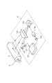
図2は、光学走査装置9の概略図を示す。この光学走査装置9は1つの感光ドラム5を露光するものであり、光学走査装置9は各感光ドラム5Y,5M,5C,5Kに対応して同様の光学走査装置9Y,9M,9C,9Kがそれぞれ設けられている。これら光学走査装置9Y,9M,9C,9Kは同様の構成であるので、以下では、その1つを光学走査装置9として代表として説明する。
[Optical scanning device]
FIG. 2 shows a schematic diagram of the
発光素子であるレーザーダイオード107(以下LD107と称する)には、レーザー駆動システム回路130の動作に基づく駆動電流が流れる。LD107は、駆動電流に応じた光量レベルでレーザー光を発光する。尚、レーザー駆動システム回路130は、後述のエンジンコントローラ122、ビデオコントローラ123に対して、電気的に接続されているLD107を駆動する為の回路である。
A driving current based on the operation of the laser
そして、LD107により発光されたレーザー光は、コリメータレンズ134によりビーム形状が整形され、かつ平行ビームとされたうえでポリゴンミラー(回転多面鏡)133により感光ドラム5の回転軸Xの方向に走査される(連続的に反射方向が変わる)。そして走査されたレーザー光は、fθレンズ132により、回転軸Xまわりに回転する被走査面としての感光ドラム9の表面上にドット状のスポットとして結像され、そのスポットがポリゴンミラー133の回転によって感光ドラム5の回転軸Xの方向に移動する(主走査)。このように、感光ドラム5上で光を走査することにより光学走査装置9は感光ドラム9を露光する。
The laser light emitted from the
一方、感光ドラム5の一端側の走査位置に対応して反射ミラー131が設けられ、走査開始位置に投射されるレーザー光を受光部である同期検出信号素子(BD検出素子)121に向けて反射させている。そして、このBD検出素子121の出力により、レーザー光の走査の開始タイミングを決定する。ここで、このレーザー光の検出における強制発光の際に、レーザー光量の自動光量調整であるところの、APC(Auto Power Control)が行われ、レーザーの発光レベルが調整される。
[レーザー駆動システム]
図3は、非画像部において、感光ドラム上にトナー付着をさせないようにし、且つかぶりや反転かぶりを発生させないように、微少発光するうえでのLD107の適切な光量レベルを自動調整するレーザー駆動システム回路(駆動手段)である。
On the other hand, a
[Laser drive system]
FIG. 3 shows a laser drive system that automatically adjusts an appropriate light amount level of the
同図において、図2で示したレーザー駆動システム回路130は、点線枠内で囲まれた回路に相当する。101、111はコンパレータ回路であり、102、112はサンプル/ホールド回路であり、103、113はホールドコンデンサである。104、114は電流増幅回路であり、105、115は基準電流源(定電流回路)であり、106、116はスイッチング回路である。107はレーザーダイオードであり、108はフォトダイオードであり、109は電流電圧変換回路であり、120はポリゴンミラー133を回転駆動するスキャナモータであり、121はBD検出素子である。尚、以下においては、フォトダイオード108をPD108と称する。また、後述にて詳しく説明するが111乃至116の部分が第1光量調整手段に相当し、101乃至106の部分が第2光量調整手段に相当する。
In FIG. 2, the laser
122はエンジンコントローラであり、プリンタの画像形成動作を統括して制御する。また、エンジンコントローラ122は、ASIC1221、CPU1222、RAM1223、及びEEPROM1224を内蔵している。ASIC1221は、後述するレーザー駆動システム回路130のAPC動作やスキャナモータ120の回転駆動の制御を行い、また、ビデオコントローラ123との通信制御なども行う。CPU1222は、ASIC1221に対して制御開始や停止等を指示する。RAM1223、EEPROM1224はCPU1222により実行されるプログラムや処理結果、ASIC1221への設定値を記憶する。
An
124はOR回路であり、エンジンコントローラ122のLdrv信号とビデオコントローラ123からのVIDEO信号が入力に接続されており、出力信号Dataは後述のスイッチング回路106へ接続されている。尚、VIDEO信号は、外部に接続されたリーダースキャナや、ホストコンピュータ等の外部機器から送られてくるプリントデータに基づき生成される。
An OR
ビデオコントローラ123から出力されるVIDEO信号は、125のイネーブル端子付きバッファに入力され、バッファの出力は前述のOR回路124に接続されている。このときイネーブル端子は、エンジンコントローラ122からのVenb信号と接続されている。また、エンジンコントローラ122は、後述のSH1信号、SH2信号、Base信号およびLdrv信号、Venb信号を出力するように接続されている。
コンパレータ回路111、101の正極端子には、それぞれ第1の基準電圧Vref11、第2の基準電圧Vref21が入力されており、出力はそれぞれサンプル/ホールド回路112、102に入力されている。サンプル/ホールド回路112、102にはそれぞれホールドコンデンサ113、103が接続されている。この基準電圧Vref11は、微少発光用の発光レベル(第1発光強度)の目標電圧として設定されている。また、基準電圧Vref21は、通常の印字用の発光レベル(第2発光強度)の目標電圧として設定されている。
The VIDEO signal output from the
The first reference voltage Vref11 and the second reference voltage Vref21 are input to the positive terminals of the
ホールドコンデンサ113、103の出力は、それぞれ電流増幅回路114、104の正極端子に入力されている。電流増幅回路114、104にはそれぞれ基準電流源115、105が接続されており、その出力はスイッチング回路116、106に入力されている。他方、電流増幅回路114、104の負極端子には、それぞれ第3の基準電圧Vref12、第4の基準電圧Vref22が入力されている。ここで先に説明したサンプル/ホールド回路112、102の出力電圧と、基準電圧Vref12、基準電圧Vref22との差分に応じて電流Io1、Io2が決定される。即ち、Vref12、22は、電流を決定する為の電圧設定である。
The outputs of the
スイッチング回路116は、入力信号BaseによりON/OFF動作する。スイッチング回路106は、パルス変調データ信号DataによりON/OFF動作する。
スイッチング回路116、106の出力端は、LD107のカソードに接続されており、駆動電流Ib、Idrvを供給している。LD107のアノードは、電源Vccに接続されている。LD107の光量をモニターするPD108のカソードは、電源Vccに接続されており、PD108のアノードは電流電圧変換回路109に接続されてモニター電流Imを電流電圧変換回路109に流すことにより、モニター電圧Vmを発生させている。このモニター電圧はコンパレータ111、101の負極端子に負帰還入力されている。
The
The output terminals of the switching
尚、図3では、エンジンコントローラ122とビデオコントローラとを別々に示しているが、その形態に限定されるわけではない。例えば、エンジンコントローラ122とビデオコントローラとの一部或いは全部を同じコントローラで構築しても良い。また、図中点線枠で囲まれたレーザー駆動回路についても、例えば、エンジンコントローラ122に一部或いは全てを内蔵させても良い。
In FIG. 3, the
[APC動作]
以下、レーザー駆動システム回路130において実行される、発光素子の2水準発光レベルに関する微少発光用APC及び印字発光用APCの動作について説明する。
[APC operation]
Hereinafter, operations of the micro light emission APC and the print light emission APC relating to the two-level light emission level of the light emitting element, which are executed in the laser
微少発光用APCでは、微少発光用の発光レベル(第1発光強度)でレーザーダイオード107が発光するよう、駆動電流Ibを調整する。また、印字発光用APCでは、通常の印字用の発光レベル(第2発光強度)でレーザーダイオード107が発光するよう、駆動電流Idrvを調整する。
In the minute emission APC, the drive current Ib is adjusted so that the
まず微少発光用APC(第2調整工程)の動作について説明する。微少発光用APCの動作では、CPU1222の指示によりASIC1221は、SH1信号を介してサンプル/ホールド回路102をホールド状態(非サンプリング期間中)に設定するとともに、入力信号Dataを介してスイッチング回路106をOFF動作状態に設定する。この入力信号Dataに関し、イネーブル端子付きバッファ125のイネーブル端子に接続されているVenb信号をディセーブル状態にし、Ldrv信号を制御し、入力信号DataをOFF状態にする。更に、ASIC1221は、SH2信号を介してサンプル/ホールド回路112をサンプリング状態に設定し、入力信号Baseを介してスイッチング回路116をON動作状態に設定する。このサンプル/ホールド回路112がサンプリング状態にある期間が、微少発光用の発光レベルを自動調整する期間に相当する。この期間、LD107には駆動電流Ibが供給される。この状態でLD107が発光すると、PD108は、LD107の発光量(発光強度)をモニターし、その発光量(発光強度)に比例したモニター電流Im1を発生させる。モニター電流Im1を電流電圧変換回路109に流すことにより、モニター電圧Vm1を発生させる。また、このモニター電圧Vm1が、目標値である第1の基準電圧Vref11と一致するように、電流増幅回路114が基準電流源115に流れるIo1をもとに駆動電流(第2駆動電流)Ibを調整する。
First, the operation of the minute emission APC (second adjustment step) will be described. In the operation of the APC for minute light emission, the
そして、印字発光用APCの実行時および通常の画像形成時(画像信号が送られている時間)には、サンプル/ホールド回路112がホールド状態にある期間であり、微少発光用の発光レベルが維持される。
During execution of printing light emission APC and during normal image formation (time during which an image signal is sent), the sample /
尚、トナーのかぶり/反転かぶり等を発生しないようにするために、画像形成中において、常にPbの光量を安定させる必要がある。 In order to prevent the occurrence of toner fog / reversal fog or the like, it is necessary to always stabilize the light quantity of Pb during image formation.
次に、印字発光用APC(第1調整工程)の動作について説明する。印字発光用APCの動作では、ASIC1221は、SH2信号を介してサンプル/ホールド回路112をホールド状態(非サンプリング期間中)に設定するとともに、入力信号Baseを介してスイッチング回路116をON動作状態に設定する。これにより、LD107には駆動電流Ibが供給された状態になる。更に、ASIC1221は、SH1信号を介してサンプル/ホールド回路102をサンプリング状態に設定し、入力信号Dataを介してスイッチング回路106をON動作状態とする。より詳細には、このとき、Ldrv信号を制御し、入力信号DataをLD107の発光状態になるように設定している。このサンプル/ホールド回路102がサンプリング状態にある期間が、印字発光用の発光レベルを自動調整する期間に相当する。この期間、LD107にはIbに対して駆動電流Idrvが重畳されたIb+Idrvが供給される。この状態でLD107が発光すると、PD108は、LD107の発光量をモニターし、その発光量に比例したモニター電流Im2(Im2>Im1)を発生させる。モニター電流Im2を電流電圧変換回路109に流すことにより、モニター電圧Vm2を発生させる。また、このモニター電圧Vm2が、目標値である第2の基準電圧Vref21と一致するように、電流増幅回路104が基準電流源105に流れるIo2をもとに駆動電流(第1駆動電流)Idrvを調整する。
Next, the operation of the printing light emission APC (first adjustment step) will be described. In the operation of the printing light emission APC, the
そして、通常の画像形成時には、サンプル/ホールド回路102がホールド状態にある期間であり、入力信号データDataに応じてスイッチング回路106がON/OFF動作し、駆動電流Idrvにパルス幅変調を与える。
During normal image formation, the sample /
図4は、LD107に流れる電流と光量の関係を示す図である。
非画像部微少発光は、駆動電流Ibを、LD107の閾値電流Ithを超え、微少発光レベルPbとなるように設定する。尚、微少発光レベル(第2発光強度)とは、そのレベルのレーザー照射によっても感光ドラムにトナー等の現像剤が実質的に帯電付着しない(顕像化されない)光量レベルで、且つトナーかぶり状態が良好な光量レベルを意味する。また微少発光レベルPbはIthを超える領域(図中A)とする。仮に、このときの微少発光レベルPbがIthに満たない領域であった場合、スペクトルの波長分布が拡がり、レーザーの定格の波長に対して広い波長分布になる。この為、感光ドラムの感度が乱れ、表面電位が不安定になってしまう。従って、微少発光レベルPbはIthを超える領域に設定することが好ましい。
FIG. 4 is a diagram showing the relationship between the current flowing through the
In the non-image area minute light emission, the drive current Ib is set so as to exceed the threshold current Ith of the
一方、通常の画像形成時は、駆動電流Ib+Idrvを、印字発光レベルPdrvの光量となる発光レベルになるように設定する。尚、印字発光レベル(第1発光強度)とは、感光ドラムへの現像剤(トナー)の帯電付着(顕像化)が飽和状態となる光量レベルを意味する。 On the other hand, during normal image formation, the drive current Ib + Idrv is set so that the light emission level becomes the light amount of the print light emission level Pdrv. Note that the print light emission level (first light emission intensity) means a light amount level at which charging (development) of developer (toner) to the photosensitive drum is saturated.
図5は、前述の微少発光レベルについて、更に詳しく説明するための図である。感光ドラム5に一次帯電ローラ7を介して帯電高圧電源(不図示)より印加された帯電電圧Vcdcは、感光ドラム5表面で帯電電位Vdとなってあらわれる。このとき、Vdは、トナー現像時の非画像部の帯電電位よりも高い電位に設定されている。そして、微少発光レベルEbg1のレーザー発光により、帯電電位Vdを、帯電電位Vd_bgに減衰させる。これは帯電電圧Vcdcを印加した後において、収束電位より高い電位が感光体表面上の所々に発生してしまう場合があり、これが現像電位Vdcと帯電電位VdのコントラストであるバックコントラストVbackを大きくし反転かぶりを誘発してしまう。
FIG. 5 is a diagram for explaining the above-mentioned minute light emission level in more detail. A charging voltage Vcdc applied to the
これに対して、上記微少発光レベルEbg1のレーザー発光により、帯電電位Vdを、帯電電位Vd_bgに減衰させると、そのような収束電位より高い電位が残存することを少なくし、少なくとも反転かぶりを抑制する。また、転写メモリがVdに現れることも良く知られている。これに対して、上記微少発光レベルEbg1のレーザー発光により、転写メモリを小さくでき、転写メモリに起因するゴースト画像の発生を少なくとも抑制できる。 On the other hand, when the charging potential Vd is attenuated to the charging potential Vd_bg by the laser light emission at the minute light emission level Ebg1, the potential higher than the convergence potential is reduced and at least the reversal fog is suppressed. . It is also well known that the transfer memory appears at Vd. On the other hand, the laser light emission with the minute light emission level Ebg1 can reduce the transfer memory, and at least suppress the generation of a ghost image due to the transfer memory.
また、上記微少発光レベルEbg1のレーザー発光は、バックコントラストVbackを適正にする機能も担っている。この観点からも、トナーの正かぶり、反転かぶりの発生を抑制できる。また、現像電位Vdcと露光電位Vlの差分値である現像コントラストVcont(=Vdc−Vl)も同時に適正にできる。これにより、現像効率を悪くしてしまったり、或いは掃き寄せの発生を抑えたり、転写・再転写のマージンを確保することができる。 Further, the laser emission of the minute emission level Ebg1 has a function of making the back contrast Vback appropriate. From this point of view as well, it is possible to suppress the occurrence of toner positive fog and reverse fog. Further, the development contrast Vcont (= Vdc−Vl), which is the difference value between the development potential Vdc and the exposure potential Vl, can be made appropriate at the same time. As a result, it is possible to deteriorate the development efficiency, suppress the occurrence of sweeping, and secure a transfer / retransfer margin.
また、帯電電圧Vcdcは、環境や感光ドラムの劣化(使用状況)等によって可変に設定される。そして、目標とする微少発光レベルの光量もそれに応じて可変に設定される。例えばVcdcの値が大きくなったら、微少発光レベルEbg1の光量も大きくなり、他方、Vcdcの値が小さくなったら微少発光レベルEbg1の光量も小さくなる。 The charging voltage Vcdc is variably set according to the environment, deterioration of the photosensitive drum (usage status), and the like. Then, the light amount of the target minute light emission level is also variably set accordingly. For example, if the value of Vcdc increases, the light amount of the minute light emission level Ebg1 also increases. On the other hand, if the value of Vcdc decreases, the light amount of the minute light emission level Ebg1 decreases.
なお、具体的に帯電電位Vdは−700V〜−600V、帯電電位Vd_bgは−550V〜−400V、現像電位Vdcは−350V、露光電位Vlは−150Vに設定するのが好ましい。 Specifically, it is preferable to set the charging potential Vd to −700 V to −600 V, the charging potential Vd_bg to −550 V to −400 V, the development potential Vdc to −350 V, and the exposure potential Vl to −150 V.
そして、通常のプリント用の印字発光レベルPdrvでLD107を発光させるときには、以下のように図3の回路を動作させる。即ち、サンプル/ホールド回路112をホールド期間に設定し、スイッチング回路116をON動作させると共に、サンプル/ホールド回路102をホールド期間に設定し、スイッチング回路106をON動作させる。これにより、LD107に駆動電流Ib+Idrvが供給される。また、スイッチング回路106のオフ状態で駆動電流Ibの微少発光レベルPbとすることが出来る。
When the
印字発光レベルPdrvは、微少発光レベルPbに相当する駆動電流Ib対して、パルス幅変調によるPWM発光レベルに相当する駆動電流Idrvを重畳した発光量となる。より具体的には、SH2、SH1、Base信号が上述の設定状態で、且つエンジンコントローラ122は、Venb信号をイネーブル状態にし、VIDEO信号によるData信号によりスイッチング回路106のON/OFFを動作させる。これにより駆動電流でIb〜Ib+Idrv間、即ち光量レベルPb〜Pdrv間の2水準の発光状態での発光が可能となる。更にPdrvの光量においては、パルスデューティーに従う時間での発光が、Pbをベースに行われている。
The print light emission level Pdrv is a light emission amount in which the drive current Idrv corresponding to the PWM light emission level by pulse width modulation is superimposed on the drive current Ib corresponding to the minute light emission level Pb. More specifically, the SH2, SH1, and Base signals are in the above-described setting state, and the
このようにレーザー駆動システム回路130を動作させることで、LD107を微少発光レベルでAPCを行い、また、レーザー発光領域における第1の発光レベルである微少発光レベルPbで発光させることが可能となる。また、ビデオコントローラ123より送出されるVIDEO信号によるData信号により、レーザー発光領域における第2のレベルである印字発光レベルPdrvの発光を行うことが可能となり、2水準の発光レベルを有することが可能となる。
By operating the laser
[光学走査装置9の起動に関する課題]
次に光学走査装置(レーザースキャナ)9の起動に関する課題について説明する。レーザースキャナ起動時には、スキャナモータを加速し、スキャナモータの回転速度が画像形成を行う為の速度(目標速度Vtg)となるように制御する(スキャナモータを立ち上げる)。この時、スキャナモータの回転速度を検知すべく、レーザーダイオード107を強制発光させ、BD検出素子121でレーザー光を検出し、BD信号を生成し、生成されたBD信号に基づいて算出されるBD周期をモニターする。即ち、スキャナモータの回転速度が速い程BD周期が短くなるという相関関係があるので、このBD周期からスキャナモータの回転速度に関連する値を得ることができ、スキャナモータの回転速度が目標速度Vtgに収束したかを判断できる。そして、スキャナモータの回転速度が目標速度Vtgに収束した(スキャナモータが立ち上がった)と判断した後、画像形成装置は画像形成動作を開始する。
[Problems related to activation of optical scanning device 9]
Next, problems relating to the activation of the optical scanning device (laser scanner) 9 will be described. When the laser scanner is activated, the scanner motor is accelerated and controlled so that the rotation speed of the scanner motor becomes the speed for forming an image (target speed Vtg) (the scanner motor is started up). At this time, in order to detect the rotation speed of the scanner motor, the
ここで、スキャナモータを立ち上げる際にBD周期をモニターする為、レーザーダイオード107を強制発光させるが、微小発光レベルPbで発光させると光量が低い為、BD検出素子121でレーザー光を検出することが難しい。この為、BD周期をモニターする際は、通常発光レベルPdrvでレーザー発光させることが好ましい。つまり、スキャナモータの立ち上げ時は印字発光用APCの動作を行いつつBD周期をモニターし、スキャナモータの回転速度が目標速度Vtgに収束した後、画像形成の為に、微少発光用APCを行い、更に2回目の印字発光用APCの動作を行う。
Here, in order to monitor the BD cycle when starting the scanner motor, the
これについて詳しく説明する。図18は、レーザースキャナ起動時におけるAPC実行によるレーザー光量、駆動電流、動作モードの時間変化を示す図である。同図において、(a)は動作モード、(b)は発光素子に供給する駆動電流、(c)は発光素子の光量を示している。 This will be described in detail. FIG. 18 is a diagram showing temporal changes in the amount of laser light, drive current, and operation mode due to APC execution when the laser scanner is activated. In FIG. 5, (a) shows the operation mode, (b) shows the drive current supplied to the light emitting element, and (c) shows the light quantity of the light emitting element.
まず、最初にスキャナモータを立ち上げの為、印字発光用APCの実行により、印字発光レベルPdrvでレーザー発光するように駆動電流Idrvを調整する。 First, in order to start up the scanner motor, the drive current Idrv is adjusted so that laser light emission is performed at the print light emission level Pdrv by executing the print light emission APC.
ここで、印字発光用APCは、本来、Ibをベースとして発光素子に供給している状態で、その光量レベルがPdrvと等しくなるように重畳分のIdrvを調整するものとして設定されている。しかし、この時点では微少発光用APCは未実行のため、Ibを発光素子に供給していない状態(Ib=0)で、Idrvを調整することになる。このようにIbを素子に供給していない状態で、発光素子(LD107)の光量レベルがPdrvとなるようにIdrvを調整すると、Idrvの値はIdrv2となる。このため、この時点ではIdrvの値の調整は完了していない。 Here, the printing light emission APC is originally set to adjust the overlap Idrv so that the light amount level becomes equal to Pdrv in a state where the light emission element is supplied based on Ib. However, at this point in time, the APC for minute light emission is not executed, so Idrv is adjusted in a state where Ib is not supplied to the light emitting element (Ib = 0). When Idrv is adjusted so that the light amount level of the light emitting element (LD 107) becomes Pdrv in a state where Ib is not supplied to the element in this way, the value of Idrv becomes Idrv2. For this reason, the adjustment of the value of Idrv is not completed at this time.
次に、スキャナモータの回転速度が目標速度Vtgに収束した後、微少発光用APCの実行により、微少発光レベルPbでレーザー発光するように駆動電流Ibを調整する。微少発光用APCは、Ibのみを発光素子に供給している状態で、その光量レベルがPbと等しくなるようにIbを調整する。従って調整されるIbの値はIb1となる。 Next, after the rotation speed of the scanner motor has converged to the target speed Vtg, the drive current Ib is adjusted so that laser emission is performed at the minute light emission level Pb by executing the minute light emission APC. The minute light emission APC adjusts Ib so that the light amount level becomes equal to Pb in a state where only Ib is supplied to the light emitting element. Therefore, the value of Ib to be adjusted is Ib1.
この後、Idrvの値の調整は完了すべく、2回目の印字発光用APCを実行すると、実行直後は、Ib1をベースとして重畳分のIdrv2が加わったIb1+Idrv2を発光素子(LD107)に供給している状態になる。このときのIb1+Idrv2は所望の値よりも大きく、その光量レベルもPdrvよりも高く、オーバーシュートした状態になる。そのため、Idrvの値は、発光素子(LD107)の光量レベルがPdrvと等しくなるようなIdrv1にまで減少するように調整される。こうして、Ib及びIdrvがそれぞれ所望の値に調整され、2水準の光量を得ることができる。なお、当然ながらIdrv1+Ib=Idrv2という関係が成り立っている。 Thereafter, when the second printing light emission APC is executed to complete the adjustment of the value of Idrv, immediately after the execution, Ib1 + Idrv2 to which the overlapped Idrv2 is added based on Ib1 is supplied to the light emitting element (LD107). It will be in a state. At this time, Ib1 + Idrv2 is larger than a desired value, and the light amount level is higher than Pdrv, resulting in an overshoot state. Therefore, the value of Idrv is adjusted so as to decrease to Idrv1 so that the light amount level of the light emitting element (LD107) becomes equal to Pdrv. Thus, Ib and Idrv are adjusted to desired values, respectively, and two levels of light intensity can be obtained. Of course, the relationship of Idrv1 + Ib = Idrv2 is established.
このように最初に印字発光用APCから実行すると、2回目の印字発光用APCを実行が必要になる場合があり、この場合、2回目の印字発光用APCの際に駆動電流のオーバーシュートが発生してしまう。しかしながら、このオーバーシュートはレーザーダイオードの定格の観点から可能な限り低減したい。 As described above, when the print light emission APC is executed first, it may be necessary to execute the second print light emission APC. In this case, the drive current overshoot occurs during the second print light emission APC. Resulting in. However, this overshoot should be reduced as much as possible from the viewpoint of the rating of the laser diode.
また、スキャナモータの回転速度が目標速度Vtgに収束した後に、微少発光用APC、及び、2回目の印字発光用APCを行わねばならず、その分だけ画像形成動作の開始を遅らせねばならない。 Further, after the rotational speed of the scanner motor has converged to the target speed Vtg, the minute light emission APC and the second print light emission APC must be performed, and the start of the image forming operation must be delayed accordingly.
また、スキャナモータの回転速度が目標速度Vtgに収束した後に2回目の印字発光用APCを行うことで、その分レーザーダイオード107の発光時間が増え、レーザーダイオード107の寿命という観点でも効率的ではない。
Further, by performing the second printing light emission APC after the rotation speed of the scanner motor has converged to the target speed Vtg, the light emission time of the
以上説明したように、レーザースキャナ起動時(スキャナモータの立上げ時)に印字発光用APCのみを行う構成だと、駆動電流がオーバーシュートするといった課題が発生する。 As described above, when only the APC for printing light emission is performed when the laser scanner is activated (when the scanner motor is started up), there arises a problem that the drive current is overshooted.
[レーザースキャナの起動シーケンス]
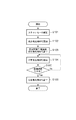
そこで、本実施例では、レーザースキャナ起動時のAPC動作を工夫している。以下、レーザースキャナ起動時(レーザー駆動システム回路130の起動時)の動作について説明する。
[Laser scanner startup sequence]
Therefore, in this embodiment, the APC operation at the time of starting the laser scanner is devised. The operation when the laser scanner is activated (when the laser
本実施例では、最初に微少発光用APCを実行し、次に印字発光用APCを実行する場合について説明する。図6は、レーザースキャナの起動シーケンスを示すフローチャートである。この処理は、CPU1222によって実行される。まず、CPU1222は、ASIC1221と通信し、S101においてスキャナモータ120の起動(回転開始及び加速)を指示する。このため、スキャナモータ120は回転を開始して加速していく。S102において微少発光APCの開始を指示する。次に、CPU1222は、S103において所定時間T1が経過するまで微少発光APCを継続し、所定時間T1経過後、サンプル/ホールド回路112をホールド状態として、微少発光用APCを終了する。ここで、所定時間T1とは、スキャナモータ120の回転速度Vが目標速度Vtgt以上となると予測される時間よりも短い時間であり、かつ、微少発光APCによる微少発光レベルの光量調整が完了するのに十分な時間で設定する。具体的には、プリンタの動作環境や寿命から推測されるレーザーの特性を考慮した上で、駆動電流Ibに調整を完了するのに必要な時間よりも長い時間となるように設定すればよい。例えば、レーザーは温度の上昇や劣化によって閾値電流Ith(図4参照)が大きくなる特性をもつため、微少発光レベルPbに相当する駆動電流Ibの値も大きくなることなどを考慮すればよい。
In the present embodiment, a case will be described in which a minute light emission APC is executed first and then a printing light emission APC is executed. FIG. 6 is a flowchart showing a startup sequence of the laser scanner. This process is executed by the
なお、本実施例では、目標速度Vtgtの80%の速度以上となると予測される時間をT1と設定している。本実施例においてはこのような設定であれば、環境によらず、微少発光APCによる微少発光レベルの光量調整が完了するのに十分な時間をとることができることがわかっている。 In the present embodiment, the time predicted to be 80% or more of the target speed Vtgt is set as T1. In this embodiment, it is known that such a setting can take a sufficient time to complete the light amount adjustment of the minute light emission level by the minute light emission APC regardless of the environment.
次のS104において、CPU1222は、印字発光用APCの開始を指示する。印字発光用APC実行中はBD周期を検出可能となる。このため、印字発光用APCの開始と同時に、ASIC1221は、スキャナモータ120の回転速度Vが目標速度Vtgtに収束するよう、検出されたBD周期に基づいて、スキャナモータ120へ加速信号(ACC)、及び又は、減速信号(DEC)を送る制御(収束制御)を行う。一方、CPU1222は、S105において、ラウンドロビン方式等の一定時間毎に、ASIC1221が算出するスキャナモータ120の回転速度Vをモニターし、目標速度Vtgtに収束したかを判別する。目標速度Vtgtに収束したかどうかの判別は、例えば、スキャナモータ120の回転速度Vが目標速度Vtgのプラスマイナス数パーセント以内に所定時間以上収まっているかどうかで等の周知の方法を用いて判別すればよい。目標速度Vtgtに収束していないと判別した場合は、モニターを継続する。一方、目標速度Vtgtに収束したと判別した場合は、S106において、CPU1222が、印字発光用APCの終了を指示し、起動シーケンスを終了する。起動シーケンスが終了すると、画像形成動作を実行する。つまり、エンジンコントローラ122は、ビデオコントローラ123からの画像データを受けてLD107により感光ドラム5へ露光動作を行う。
In the next S104, the
図7は、図6の起動シーケンスの処理における、(a)動作モード、(b)レーザー駆動電流、(c)レーザー光量、(d)BD信号、(e)スキャナモータ回転速度の時間変化を示す図である。同図(a)、(b)、(c)においては、微少発光用APCの実行により、微少発光レベルPbに相当する駆動電流Ibが調整され、次の印字発光用APCの実行により、印字発光レベル(通常発光レベル)Pdrvに相当する駆動電流Ib+Idrvが調整される。このように、スキャナモータの立上げる間に、微少発光用APC、印字発光用APCの順でAPCを実行することにより、1回目の印字発光用APCでIdrvを所望の値に調整し、オーバーシュートの発生を抑えることができ、効率的にIb、Idrvを調整することが可能となる。 FIG. 7 shows temporal changes in (a) operation mode, (b) laser drive current, (c) laser light quantity, (d) BD signal, and (e) scanner motor rotation speed in the processing of the startup sequence of FIG. FIG. In (a), (b), and (c), the driving current Ib corresponding to the minute light emission level Pb is adjusted by executing the minute light emission APC, and the printing light emission is performed by executing the next printing light emission APC. The drive current Ib + Idrv corresponding to the level (normal light emission level) Pdrv is adjusted. In this way, by executing APC in the order of micro light emission APC and print light emission APC during the startup of the scanner motor, the first print light emission APC adjusts Idrv to a desired value, and overshoots. Can be suppressed, and Ib and Idrv can be adjusted efficiently.
また、同図(a)、(d)、(e)においては、スキャナモータ起動に伴いASIC1221が出力する加速指示によりポリゴンミラー133が回転し始める。これと同時に微少発光用APCの実行により、LD107は発光を開始し、ポリゴンミラー133に反射されたレーザー光がBD検出素子121へ入力されるものの、LD107は光量の弱い状態での微少発光レベルPbで発光しているため、BD検出素子121はレーザー光を検出しない。よって、BD信号は生成されず、ASIC1221は加速指示を出力し、スキャナモータの回転速度を上昇させる。次の印字発光用APCの実行により、LD107は通常発光レベルで発光しているため、BD検出素子121はレーザー光を検出し、BD信号を生成する。ASIC1221は、生成されたBD信号を入力し、BD信号に基づいてBD周期を算出する。このBD周期をスキャナモータの回転速度として、CPU1222がモニターし、目標速度Vtgtに到達しているかを判断する。
In FIGS. 9A, 9D, and 9E, the
以上、説明したように、本実施例では、最初に微少発光用APCを実行し、次に印字発光用APCを実行するようにレーザースキャナを起動させた。つまり、レーザースキャナは、スキャナモータ120が回転を開始した後で且つ印字発光用APCを行う前に微小発光用APCを実行した。このようにすることで、LD107を微少発光レベルPb、および印字発光レベルPdrvの2水準の発光状態で発光させる上で、スキャナモータを立ち上げの為に通常発光レベルPdrvで発光しつつも、2回目の印字発光用APCの際に駆動電流がオーバーシュートすることを抑えることができる。従って、効率的にIb、Idrvを調整することが可能となる。つまり、1つの発光素子が2つの発光強度で発光するよう適切に調整することが可能となる。
As described above, in the present embodiment, the laser scanner is activated so that the minute light emission APC is executed first and then the print light emission APC is executed. That is, the laser scanner executed the minute light emission APC after the
<実施例2>
次に実施例2について説明する。実施例2は、実施例1に対し、レーザースキャナの起動シーケンスの一部が異なる。即ち、実施例2では、第1微少発光用APCと印字発光用APCを複数回繰り返し行う起動シーケンスについて説明する。その他の画像形成装置の構成、及び、光学走査装置9の構成、レーザー駆動システム回路130等の構成は実施例1と同様であるため説明を省略し、実施例1と異なる点についてのみ説明を行う。
<Example 2>
Next, Example 2 will be described. The second embodiment is different from the first embodiment in a part of the startup sequence of the laser scanner. That is, in the second embodiment, a startup sequence in which the first micro light emission APC and the print light emission APC are repeated a plurality of times will be described. Other configurations of the image forming apparatus, the configuration of the
実施例1では、レーザースキャナ起動時において、スキャナモータの回転速度が目標速度に到達するまでに微少発光用APCと印字発光用APCを1回ずつ行う起動シーケンスについて説明した。ここで、レーザー駆動システム回路130はアナログ回路で構成されるため、印字発光用APCの実行中にホールド状態にある駆動電流Ibは、リーク電流により徐々に減少する。そこで、本実施例ではより精度良く駆動電流Ibを調整可能な起動シーケンスについて説明する。
In the first embodiment, when the laser scanner is activated, the activation sequence in which the minute light emission APC and the print light emission APC are performed once until the rotation speed of the scanner motor reaches the target speed has been described. Here, since the laser
図8は、本実施例に係るレーザースキャナの起動シーケンスを示すフローチャートである。この処理は、CPU1222によって実行される。
S201〜S204においては実施例1で説明したS101〜S104と同様の処理を行う。つまり、先ず微小発光用APCを実行する。尚、S203の所定時間T2は、S103の所定時間T1としても良い。S205において、CPU1222は、所定時間T3が経過するまで印字発光用APCを継続する。ここで、所定時間T3とは、ASIC1221がBD周期を算出するのに十分な時間である。つまり、印字発光用APCの実行期間中に少なくとも連続2回以上のBD信号を検出できる時間である。
FIG. 8 is a flowchart showing a startup sequence of the laser scanner according to the present embodiment. This process is executed by the
In S201 to S204, the same processing as S101 to S104 described in the first embodiment is performed. That is, first, micro-light emission APC is executed. Note that the predetermined time T2 in S203 may be the predetermined time T1 in S103. In S205, the
次のS206において、CPU1222は、ASIC1221により算出されたスキャナモータの回転速度に対応する値(BD周期)に基づいて、スキャナモータの回転速度が所定速度Vint以上かを判別する。所定速度Vintより遅い場合はS202に戻り、再度微少発光用APCの開始を指示する。一方、所定速度Vint以上の場合はS207へ進み、印字発光用APCを継続する。また、同時に、実施例1と同様に、ASIC1221がスキャナモータ120の回転速度Vを目標速度Vtgtへ収束させる収束制御を実行する。一方でCPU1222は、S208、S209で、実施例1のS105、S106と同様の処理を行ったのち、起動シーケンスを終了する。ここで、所定速度Vintとは、スキャナモータの目標速度Vtgtよりも低い速度である。また、所定速度Vintは、なるべく目標速度Vtgtに近い速度がよく、目標速度Vtgtの80〜90%の速度に設定するのが望ましい。その理由は、微少発光用APCと印字発光用APCの実行の繰り返し期間をなるべく長くとるためである。しかしながら、あまりに目標速度Vtgtに近い速度で設定しまうと、微少発光用APCを実行中はBD信号の生成が難しいので、微少発光用APCの実行中に目標速度Vtgtを大きく超えてしまい、スキャナモータの速度を目標速度Vtgtに収束させるのに時間がかかってしまう場合がある。よって、これらを考慮して、所定速度Vintは、目標速度Vtgtに対して所定の割合を持たせた速度に設定している。
In the next S206, the
図9は、図8の起動シーケンスの処理における、(a)動作モード、(b)レーザー駆動電流、(c)レーザー光量、(d)BD信号、(e)スキャナモータ回転速度の時間変化を示す図である。 9 shows (A) operation mode, (b) laser drive current, (c) laser light quantity, (d) BD signal, and (e) scanner motor rotation speed over time in the startup sequence process of FIG. FIG.
同図(a)、(b)、(c)においては、微少発光用APCと印字発光用APCの実行を繰り返し行いながらIbおよびIdrvが調整される。更に、微少発光用APCと印字発光用APCの実行を繰り返し行うことで、リーク電流による駆動電流の減少を抑えながら所望の光量に調整された状態で起動シーケンスを終えることができる。 In (a), (b), and (c) of the figure, Ib and Idrv are adjusted while repeatedly executing the APC for minute emission and the APC for printing emission. Furthermore, by repeating the execution of the minute light emission APC and the printing light emission APC, the start-up sequence can be completed in a state where the light intensity is adjusted to a desired light amount while suppressing a decrease in the drive current due to the leakage current.
また、同図(a)、(d)、(e)においては、CPU1222は、微少発光用APCと印字発光用APCが実行される毎に、ASIC1221が算出するスキャナモータ120の回転速度Vが所定速度Vint以上かを判別する。所定速度Vintに到達するまでの期間、印字発光用APCの実行中はBD検出素子121よりBD信号が生成されるものの、所定速度Vint以下のため加速状態は維持される。所定速度Vint以上と判別した場合の動作については実施例1と同様である。
In FIGS. 9A, 9D, and 9E, the
以上、説明したように、本実施例では、最初に微少発光用APCを実行し、次に印字発光用APCを実行するようにレーザースキャナを起動させた。つまり、レーザースキャナは、スキャナモータ120が回転を開始した後で且つ印字発光用APCを行う前に微小発光用APCを実行した。このようにすることで、LD107を微少発光レベルPb、および印字発光レベルPdrvの2水準の発光状態で発光させる上でスキャナモータを立ち上げの為に通常発光レベルPdrvで発光しつつも、2回目の印字発光用APCの際に駆動電流がオーバーシュートすることを抑えることができる。従って、効率的にIb、Idrvを調整することができる。つまり、1つの発光素子が2つの発光強度で発光するよう適切に調整することが可能となる。
As described above, in the present embodiment, the laser scanner is activated so that the minute light emission APC is executed first and then the print light emission APC is executed. That is, the laser scanner executed the minute light emission APC after the
また、本実施例では、レーザースキャナの起動時に、微少発光用APCと印字発光用APCの実行をそれぞれ交互に複数回繰り返すことで、実施例1に比べてより安定して精度良く通常発光レベル及び微小発光レベルの光量調整を行うことが可能となる。 Further, in this embodiment, when the laser scanner is started, the execution of the micro light emission APC and the printing light emission APC is alternately repeated a plurality of times, so that the normal light emission level and the stable light emission level can be improved more stably than in the first embodiment. It is possible to adjust the light amount at a minute light emission level.
<実施例3>
次に実施例3について説明する。実施例3は、実施例1に対し、レーザースキャナの起動シーケンスの一部が異なる。即ち、微少発光用APCと印字発光用APCの実行に加えレーザー消灯期間を加え、これを複数回繰り返し行う起動シーケンスについて説明する。その他の、本実施例に係る画像形成装置の構成、および光学走査装置9の構成、レーザー駆動システム回路130等の構成は実施例1と同様であるため説明を省略し、実施例1と異なる点についてのみ説明する。
<Example 3>
Next, Example 3 will be described. The third embodiment is different from the first embodiment in part of the startup sequence of the laser scanner. That is, a start sequence in which a laser extinction period is added in addition to the execution of the minute light emission APC and the print light emission APC and this is repeated a plurality of times will be described. Other configurations of the image forming apparatus according to the present embodiment, the configuration of the
ここで、実施例2では、レーザースキャナ起動時に、微少発光用APCと印字発光用APCを複数回繰り返し実行する起動シーケンスについて説明した。このような起動シーケンスでは、起動シーケンスの処理中においてレーザーは常時発光している状態となる。一方で、感光ドラム上にレーザー照射を繰り返すことによって、ドラム面の露光感度は劣化していく、またレーザーダイオードも劣化していく。そのため、起動シーケンス中、常時発光していると、感光ドラム上にレーザー照射する頻度が増え、感光ドラム及び又はレーザーダイオードの寿命を早める。そこで、本実施例では、安定して精度良く通常発光レベル及び微小発光レベルの光量調整を行いつつも、感光ドラム上にレーザー照射する頻度を減らす起動シーケンスについて説明する。 Here, in the second embodiment, the activation sequence in which the minute emission APC and the printing emission APC are repeatedly executed a plurality of times when the laser scanner is activated has been described. In such an activation sequence, the laser is always on during the activation sequence. On the other hand, by repeating laser irradiation on the photosensitive drum, the exposure sensitivity of the drum surface deteriorates and the laser diode also deteriorates. Therefore, if the light is constantly emitted during the start-up sequence, the frequency of laser irradiation on the photosensitive drum increases, and the life of the photosensitive drum and / or laser diode is shortened. Therefore, in this embodiment, a startup sequence for reducing the frequency of laser irradiation on the photosensitive drum while adjusting the light amount of the normal light emission level and the minute light emission level stably and accurately will be described.
図10は、本実施例に係るレーザースキャナの起動シーケンスを示すフローチャートである。この処理は、CPU1222によって実行される。まず、CPU1222は、ASIC1221と通信し、S301においてスキャナモータを起動し、S302において所定時間T4待つ。このときレーザー駆動システム回路130は動作しておらず、LD107は消灯状態である。ここで、所定時間T4とは、スキャナモータが目標速度に到達するまでの期間のうち、微少発光用APCおよび印字発光用APCを実行する期間と、スキャナモータの回転速度をモニターする期間を除いた期間であれば任意の時間で設定すればよい。例えば、目標速度の1/3の速度に到達すると予測される時間等に設定すればよい。
FIG. 10 is a flowchart showing a startup sequence of the laser scanner according to the present embodiment. This process is executed by the
次のS303〜S306の処理においては実施例2で説明したS202〜S205と同様の処理を行う。ここで、S304の所定時間T5およびS306の所定時間T6は、S203の所定時間T2およびS205の所定時間T3としてもよいし、それよりも短く設定してもよい。次のS307において、スキャナモータの回転速度が所定の速度Vintに以上となっているかを判別する。スキャナモータの回転速度が所定の速度によりも遅いと判別した場合、S309へ進み、印字発光用APCを終了し、LD107を消灯する。つまり、図3に示したレーザー駆動システム回路130において、CPU1222は、サンプル/ホールド回路112、102をホールド状態にし、更にスイッチング回路116、106をOFF状態にする。そして、次のS311において、CPU1222は、所定時間T7が経過するまで待つ。ここで、所定時間T7とはS304およびS306の処理と同様の時間としても良い。所定時間T7が経過すると、S303に戻る。一方、S307において、スキャナモータの回転速度が所定の速度Vint以上であると判別した場合、印字発光用APCを継続する。また、同時に、実施例1と同様に、ASIC1221がスキャナモータ120の回転速度Vを目標速度Vtgtへ収束させる収束制御を実行する。一方でCPU1222は、S308、S309、S312の処理を行う。なお、この処理はS207〜S209と同様の処理であるので説明は省略する。
In the next processing of S303 to S306, the same processing as S202 to S205 described in the second embodiment is performed. Here, the predetermined time T5 of S304 and the predetermined time T6 of S306 may be the predetermined time T2 of S203 and the predetermined time T3 of S205, or may be set shorter than that. In next step S307, it is determined whether the rotation speed of the scanner motor is equal to or higher than a predetermined speed Vint. When it is determined that the rotation speed of the scanner motor is slower than the predetermined speed, the process proceeds to S309, the printing light emission APC is terminated, and the
図11は、図10の起動シーケンスの処理における、(a)動作モード、(b)レーザー駆動電流、(c)レーザー光量、(d)BD信号、(e)スキャナモータ回転速度の時間変化を示す図である。同図(a)、(b)、(c)においては、スキャナモータを起動すると、S302の所定時間T4経過した後、微少発光用APCの実行を開始する。その後、微少発光用APCと印字発光用APC、レーザー消灯の実行を繰り返し行いながらIbおよびIdrvが調整される。 FIG. 11 shows temporal changes in (a) operation mode, (b) laser drive current, (c) laser light quantity, (d) BD signal, and (e) scanner motor rotation speed in the processing of the startup sequence of FIG. FIG. In (a), (b), and (c) of the figure, when the scanner motor is started, the execution of the minute light emission APC is started after a predetermined time T4 in S302. Thereafter, Ib and Idrv are adjusted while repeatedly performing the micro emission APC, the printing emission APC, and the laser extinction.
また、同図(a)、(d)、(e)においては、実施例2と同様に、CPU1222は、微少発光用APCと印字発光用APCが実行される(2回目以降はレーザー消灯含む)毎に、ASIC1221が算出するスキャナモータ120の回転速度Vが所定速度Vintに以上かを判別する。Vintに到達するまでの期間、レーザー消灯する期間が存在するものの、ASIC1221は、スキャナモータの回転速度を十分に算出できるだけの印字発光用APCの期間が設定されている。スキャナモータ120の回転速度VがVintに以上となった後の動作には実施例2と同様であるため説明を省略する。
In FIGS. 9A, 9D, and 9E, as in the second embodiment, the
以上、説明したように、本実施例では、最初に微少発光用APCを実行し、次に印字発光用APCを実行するようにレーザースキャナを起動させた。つまり、レーザースキャナは、スキャナモータ120が回転を開始した後で且つ印字発光用APCを行う前に微小発光用APCを実行した。このようにすることで、LD107を微少発光レベルPb、および印字発光レベルPdrvの2水準の発光状態で発光させる上で、スキャナモータを立ち上げの為に通常発光レベルPdrvで発光しつつも、2回目の印字発光用APCの際に駆動電流がオーバーシュートすることを抑えることができる。従って、効率的にIb、Idrvを調整することができる。つまり、1つの発光素子が2つの発光強度で発光するよう適切に調整することが可能となる。
As described above, in the present embodiment, the laser scanner is activated so that the minute light emission APC is executed first and then the print light emission APC is executed. That is, the laser scanner executed the minute light emission APC after the
また、本実施例では、レーザースキャナの起動時に、微少発光用APCと印字発光用APCの実行をそれぞれ交互に複数回繰り返すことで、実施例1に比べてより安定して精度良く通常発光レベル及び微小発光レベルの光量調整を行うことが可能となる。また、スキャナモータが目標速度に収束するまでにレーザーを消灯する期間を設けることで、安定して精度良く通常発光レベル及び微小発光レベルの光量調整を行いつつも、感光ドラム上にレーザー照射する頻度を減らすことができる。これにより、実施例2よりも感光ドラムやレーザーダイオードの寿命を延ばすことが可能となる。なお、上記の説明では、微小発光用APCの前にS302でレーザーが消灯している期間(所定時間T4)を設けた。しかし、S302でレーザーを消灯している期間(所定時間T4)を設けず、S310、S311でレーザーが消灯している期間(所定時間T7)だけを設けてもよい。その逆に、S302でレーザーを消灯している期間(所定時間T4)を設ければ、S310、S311でレーザーが消灯している期間(所定時間T7)を設けなくてもよい。また、S310、S311でレーザーが消灯している期間(所定時間T7)は、2回のうち1回だけ設けるようにしてもよい。 Further, in this embodiment, when the laser scanner is started, the execution of the micro light emission APC and the printing light emission APC is alternately repeated a plurality of times, so that the normal light emission level and the stable light emission level can be improved more stably than in the first embodiment. It is possible to adjust the light amount at a minute light emission level. In addition, by providing a period during which the laser is turned off before the scanner motor converges to the target speed, the frequency of laser irradiation on the photosensitive drum while adjusting the light amount of the normal light emission level and minute light emission level stably and accurately. Can be reduced. Thereby, it is possible to extend the life of the photosensitive drum and the laser diode as compared with the second embodiment. In the above description, a period (predetermined time T4) in which the laser is extinguished in S302 is provided before the micro-emission APC. However, the period during which the laser is turned off in S302 (predetermined time T4) may not be provided, and the period during which the laser is turned off in S310 and S311 (predetermined time T7) may be provided. On the contrary, if the period during which the laser is turned off in S302 (predetermined time T4) is provided, the period during which the laser is turned off in S310 and S311 (predetermined time T7) may not be provided. In addition, the period during which the laser is turned off in S310 and S311 (predetermined time T7) may be provided only once out of the two times.
いずれにしても、S307でスキャナモータ120の回転を開始してから回転速度がVintになるまでにレーザー消灯している期間(所定時間T4、所定時間T7)を少なくとも1回設ければよい。このようにしても、上記と同様の効果を得ることができる。
In any case, the laser extinguishment period (predetermined time T4, predetermined time T7) may be provided at least once after the rotation of the
また、上記の説明では、レーザーを消灯する期間を微小発光用APCの前に設けたが、これに限られない。つまり、微小発光用APCと印字発光用APCの間にレーザーを消灯する期間を設けることや、微小発光用APC及び印字発光用APCを複数回実行する構成であれば、印字発光用APCの後で微小発光用APCの前にレーザーを消灯する期間を設けてもよい。このようにしても上記と同様の効果を得ることができる。 In the above description, the period during which the laser is turned off is provided in front of the micro-emission APC. However, the present invention is not limited to this. In other words, if there is a period during which the laser is extinguished between the micro light emission APC and the print light emission APC, or if the micro light emission APC and the print light emission APC are executed a plurality of times, the print light emission APC is followed. A period during which the laser is turned off may be provided before the minute emission APC. Even if it does in this way, the effect similar to the above can be acquired.
<実施例4>
次に実施例4について説明する。上述の実施例1〜3では、最初に微小発光用APCを行うレーザースキャナの起動シーケンスについて説明したが、実施例4は、最初に印字発光用APCを行うレーザースキャナの起動シーケンスについて説明する。尚、本実施例に係る画像形成装置の構成、および光学走査装置8の構成、レーザー駆動システム回路130の構成は実施例1と同様であるため説明を省略し、実施例1と異なる点についてのみ説明する。
<Example 4>
Next, Example 4 will be described. In the above-described first to third embodiments, the startup sequence of the laser scanner that performs APC for minute emission is described first, but in the fourth embodiment, the startup sequence of the laser scanner that performs APC for printing emission first is described. The configuration of the image forming apparatus according to the present embodiment, the configuration of the optical scanning device 8, and the configuration of the laser
図12は、本実施例に係るレーザースキャナの起動シーケンスを示すフローチャートである。この処理は、CPU1222によって実行される。まず、CPU1222は、S401においてスキャナモータの起動を指示し、S402において印字発光用APCの開始をレーザー駆動システム回路130へ指示する。次のS403においてCPU1222は、印字発光用APCが所定時間T8の期間実行されたら、印字発光用APCを終了する。尚、所定時間T8については後述する。その後、S404において微小発光用APCを開始する。その後のS405〜S407においては、実施例1で説明したS103〜S106と同様の処理を行う。なお、S406へ進んだ場合、印字発光用APCを継続すると、同時に、実施例1と同様に、ASIC1221がスキャナモータ120の回転速度Vを目標速度Vtgtへ収束させる収束制御を実行する。
FIG. 12 is a flowchart showing a startup sequence of the laser scanner according to the present embodiment. This process is executed by the
[所定時間T8の説明]
図13は、前述のS403の処理における所定時間T8を説明するためのLD107に流れる電流と光量の関係示す図である。同図実線で表わされる特性において、上記の[レーザースキャナの起動に関する課題]で説明した様に、印字発光用APCの実行から最初に実行した場合、2回目の印字発光用APCの実行直後のLD107に供給される駆動電流は、I1に対してI2が重畳されたI1+I2となる。これがオーバーシュートとなって現れる。その後、I1+Idrv=I2となるように駆動電流Idrv(=I2−I1)を減少させるように調整する。この駆動電流I1+I2に相当する光量レベルが定格レベルPlimitを超えてしまう恐れがある。このPlimitを超えないようにするためには、最初の印字発光用APCの実行により、調整期間中のIdrvの値が所定の電流値に達する前に微少発光用APCへ切り替えれば良い。ここで、所定の電流値とは、Plimitに相当する駆動電流をIlimitとすると、Ilimit−I1としても良いし、これ以下の値としても良い。
[Explanation of predetermined time T8]
FIG. 13 is a diagram showing the relationship between the current flowing through the
また、同図破線で表わされる特性のように、レーザーは温度上昇や劣化によって閾値電流Ithが大きくなる特性をもつため、微少発光レベルPbに相当する駆動電流IbおよびIlimitの値も大きくなる(図中のI1’、Ilimit’)。但し、閾値電流Ithを超える領域の特性の傾きは、Ithの変化によらずほぼ一定である。よって、IbおよびIlimitが、Ithを超える領域に位置していれば、Ilimit−Ibの値はIthの値によらずほぼ一定である。 Further, as shown by the broken line in the figure, since the laser has a characteristic that the threshold current Ith increases due to temperature rise or deterioration, the values of the drive currents Ib and Ilimit corresponding to the minute light emission level Pb also increase (FIG. I1 ′, Ilimit ′). However, the slope of the characteristic in the region exceeding the threshold current Ith is substantially constant regardless of the change in Ith. Therefore, if Ib and Ilimit are located in a region exceeding Ith, the value of Ilimit−Ib is substantially constant regardless of the value of Ith.
ここで、最初に印字発光用APCをする場合、レーザー駆動電流Idrvは0から徐々に大きくなっていく。従って、所定時間T8は、印字発光用APCの実行した際に、駆動電流Idrvの値がIlimit−Ibとなる期間、又は、Ilimit−Ibとなる期間よりも短い期間として設定されている。つまり、所定時間T8は、Idrvが、Idrv≦Ilimit−Ibをみたす範囲にある時間であれば任意の値で良い。なお、この時間は予め測定した結果に基づいた設計値として算出すれば良い。印字発光用APCをこのように設定された所定時間T8だけやることにより、Idrvは、Idrv_ini(Idrv_ini≦Ilimit−Ib)となるよう調整されることになる。つまり、所定時間T8だけ印字発光用APCを行うことは、駆動電流Idrv_iniによって、通常の印字用の発光レベル(第2発光強度)よりも低い発光レベル(第3発光強度)で発光するよう、駆動電中Idrvを調整するAPC(第3調整工程)であるといえる。 Here, when the APC for printing light emission is first performed, the laser drive current Idrv gradually increases from zero. Therefore, the predetermined time T8 is set as a period in which the value of the drive current Idrv becomes Ilimit-Ib or a period shorter than the period in which Ilimit-Ib is obtained when the printing light emission APC is executed. That is, the predetermined time T8 may be any value as long as Idrv is in a range satisfying Idrv ≦ Ilimit−Ib. In addition, what is necessary is just to calculate this time as a design value based on the result measured beforehand. By performing the printing light emission APC for the predetermined time T8 set in this way, Idrv is adjusted to be Idrv_ini (Idrv_ini ≦ Ilimit−Ib). That is, the printing light emission APC for the predetermined time T8 is driven so as to emit light at a light emission level (third light emission intensity) lower than the normal printing light emission level (second light emission intensity) by the drive current Idrv_ini. It can be said that this is an APC (third adjustment step) for adjusting the electric power Idrv.
図14は、図12の起動シーケンスの処理における、(a)動作モード、(b)レーザー駆動電流、(c)レーザー光量、(d)BD信号、(e)スキャナモータの回転速度の時間変化を示す図である。同図(a)、(b)、(c)においては、スキャナモータ120を起動すると、印字発光用APCの実行を開始し、所定時間T8が経過すると微少発光用APCに切り替える。駆動電流Idrvは、Idrv_iniとなる。その後、微少発光用APCの実行を開始し、駆動電流Ibは、微少発光レベルPbに相当するIb1に調整される。次に、2回目の印字発光用APCの実行により、駆動電流Idrvは、Ib1に対して調整途中のIdrv_iniが重畳された駆動電流から調整を開始する。この時点での駆動電流に相当する光量レベルは、定格レベルPlimit以下の値であるため、オーバーシュートによる定格超えは発生しない。その後、駆動電流Idrvは、印字発光レベルPdrvに相当する駆動電流Ib1+Idrv1となるようにIdrv=Idrv1に調整される。
FIG. 14 shows changes over time in (a) operation mode, (b) laser drive current, (c) laser light quantity, (d) BD signal, and (e) scanner motor rotation speed in the processing of the startup sequence of FIG. FIG. In (a), (b), and (c) of the figure, when the
また、同図(a)、(d)、(e)においては、スキャナモータ120を起動し、加速状態で回転駆動するとともに印字発光用APCを実行し、所定時間T8後に微少発光用APCを実行する。このT8の期間、LD107に調整途中のIdrvが供給された状態の発光レベルであるものの、スキャナモータ120の回転速度Vは目標速度Vtgt以下のため、スキャナモータ120の加速状態を維持させる。以降は実施例1と同様であるため説明を省略する。
Also, in FIGS. 4A, 4D, and 4E, the
以上、説明したように、本実施例では、最初に印字発光用APCを実行しても、駆動電流Idrvの調整が完了する前に印字発光用APCを終了し、微少発光用APCを実行するようにレーザースキャナを起動させた。これにより、LD107を微少発光レベルPb、および印字発光レベルPdrvの2水準の発光状態で発光させる上で、印字発光用APCを最初に行った場合でも、2回目の印字発光用APCの際に駆動電流がオーバーシュートすることを抑えることができる。従って、効率的にIb、Idrvを調整することが可能となる。つまり、1つの発光素子が2つの発光強度で発光するよう適切に調整することが可能となる。
As described above, in this embodiment, even if the printing light emission APC is executed first, the printing light emission APC is terminated before the adjustment of the drive current Idrv is completed, and the minute light emission APC is executed. The laser scanner was activated. Thus, the
尚、本実施例の起動シーケンスは、実施例2のように印字発光用APCと微少発光用APCを複数回繰り返し行うようにしてもよい。また、実施例3のように微少発光用APC、及び、印字発光用APC、及び、レーザー消灯の実行を複数回繰り返し実行するようにしてもよい。 Note that the activation sequence of the present embodiment may be performed by repeating the printing light emission APC and the minute light emission APC a plurality of times as in the second embodiment. In addition, as in the third embodiment, the execution of the micro light emission APC, the print light emission APC, and the laser extinction may be repeated a plurality of times.
また、S403の処理は、環境や感光ドラムの劣化等によって可変に設定される微少発光レベルの光量に応じて、所定時間T8も可変に設定してもよい。具体的には、所定時間T3の値を感光ドラムの劣化状況や環境に応じて複数用意しておき、感光ドラムの劣化状況や環境を検知あるいは予測して定期的に所定時間T8を再設定すればよい。また、所定時間T8を再設定するタイミングは、微少発光レベルの光量を再設定した際などがよい。また、微小発光レベルの光量は、感光ドラムの劣化状況や環境に応じて再設定する構成となっている。このため、所定時間T8を複数用意しなくても、微少発光レベルの光量を再設定したときの光量の変化率に基づく演算によって所定時間T8を算出する構成であってもよい。 In the process of S403, the predetermined time T8 may be variably set according to the light amount of the minute light emission level that is variably set according to the environment, deterioration of the photosensitive drum, or the like. Specifically, a plurality of values of the predetermined time T3 are prepared according to the deterioration state and environment of the photosensitive drum, and the predetermined time T8 is periodically reset by detecting or predicting the deterioration state and environment of the photosensitive drum. That's fine. Further, the timing for resetting the predetermined time T8 is preferably when the light amount of the minute light emission level is reset. Further, the light amount at the minute light emission level is reset according to the deterioration state and environment of the photosensitive drum. For this reason, the configuration may be such that the predetermined time T8 is calculated by calculation based on the change rate of the light amount when the light amount of the minute light emission level is reset, without preparing a plurality of the predetermined time T8.
<実施例5>
本発明の第5の実施形態では、印字発光用APCから最初に実行した場合でも、駆動電流Ibを予め所定の値に設定しておくことのできるレーザー駆動システム回路について説明する。尚、本実施例に係る画像形成装置の構成、および光学走査装置9等の構成は第1実施例と同様であるため説明を省略する。
<Example 5>
In the fifth embodiment of the present invention, a laser drive system circuit in which the drive current Ib can be set to a predetermined value even when it is first executed from the print light emission APC will be described. Note that the configuration of the image forming apparatus according to the present embodiment and the configuration of the
図15は、図3のレーザー駆動システム回路に対して、コンデンサ119と、スイッチ118と、スイッチ118を制御するBase2信号を追加した点が異なる。スイッチ118の一端には、コンデンサ119が接続され、他端にはサンプル/ホールド回路112が接続されている。
FIG. 15 is different from the laser drive system circuit of FIG. 3 in that a
Base2信号により、スイッチ118がサンプル/ホールド回路112と電流増幅回路114を接続する場合、実施例1と同様にサンプル/ホールド回路112の状態に応じたAPC動作を行う。一方、コンデンサ119と電流増幅回路114を接続する場合、電源投入とともにコンデンサ119に蓄えられた所定電圧Vini1と基準電圧Vref12との差分に応じた所定電流Iini1が決定され、これを駆動電流IbとしてLD107へ供給する。尚、所定電流Iini1は、後述するが、Iini1がIb〜Ib+Idrv間の値をとるように、電源投入後コンデンサ119に蓄えられる所定電圧Vini1を設定している。
When the
以下、図15のレーザー駆動システム回路の動作について、図12の起動シーケンスフローチャートの処理内容を一部変更し、その変更点を中心に説明する。
S402においてCPU1222は、印字発光用APCの実行を指示するとともに、Base2信号を介してコンデンサ119と電流増幅回路114を接続状態に制御する。つまり、所定の値のIbとしてIini1(所定の値の第2駆動電流)がLD107に供給されることになる。これにより、LD107にはIini1+Idrvの駆動電流が供給される。次のS403においてCPU1222は、所定時間経過するまで待つ。尚、所定時間T8は実施例1と同様にIdrvの調整が十分に完了する時間であればよい。これにより、駆動電流Idrvは、Iini1+Idrvに相当するLD107の光量が印字発光レベルPdrvとなるIdrv_iniとなるように調整される。
Hereinafter, the operation of the laser drive system circuit of FIG. 15 will be described with a part of the processing content of the startup sequence flowchart of FIG.
In S402, the
ここで、Vini1は、Iini1が、光量レベルがPbとなるIb1以上、且つ、光量レベルがPdrvとなるIb1+Idrv1未満の値をとるように設定するのが望ましい。そうすると、Idrvは必ずIdrv1以下の値に調整されるため、2回目に印字発光用APCを実行した際にオーバーシュートを発生させないようにすることが可能になる。 Here, Vini1 is desirably set so that Iini1 takes a value not less than Ib1 at which the light amount level becomes Pb and less than Ib1 + Idrv1 at which the light amount level becomes Pdrv. Then, since Idrv is always adjusted to a value equal to or less than Idrv1, it is possible to prevent an overshoot from occurring when the print light emission APC is executed for the second time.
次のS404においてCPU1222は、微少発光用APCの実行を指示するとともに、Base2信号をサンプル/ホールド回路112と電流増幅回路114と接続状態に制御する。以降の処理(S405〜S408)ではこの接続状態を継続しながら行う。なお、S405〜S408は実施例4と同様の処理であるので説明は省略する。
In the next step S404, the
図16は、本実施例に係る図12の起動シーケンスの処理における、(a)動作モード、(b)レーザー駆動電流、(c)レーザー光量、(d)BD信号、(e)スキャナモータ回転速度の時間変化を示す図である。同図(a)、(b)、(c)においては、スキャナモータを起動すると、印字発光用APCの実行を開始する。このとき、コンデンサ119に蓄えられたVini1により供給されるIini1をベースとした状態からIdrvの調整を開始し、Idrvの値はIdrv_iniとなる。その後、微少発光用APCの実行により、IbはIb1に調整される。次に、2回目の印字発光用APCの実行により、Ib1+Idrv_iniの状態からIdrvの調整を開始し、Idrvの値はIdrv1となる。
FIG. 16 shows (a) operation mode, (b) laser drive current, (c) laser light quantity, (d) BD signal, and (e) scanner motor rotation speed in the processing of the activation sequence of FIG. 12 according to the present embodiment. It is a figure which shows the time change of. In (a), (b), and (c) of the figure, when the scanner motor is activated, execution of APC for printing light emission is started. At this time, adjustment of Idrv is started from a state based on Iini1 supplied by Vini1 stored in the
また、同図(a)、(d)、(e)においては、最初の印字発光用APCの実行中はBD検出素子121よりBD信号が生成されるものの、Vtgt未到達のため加速状態は維持される。以降は実施例1と同様であるため説明を省略する。
Further, in FIGS. 9A, 9D, and 9E, the BD signal is generated from the
以上、説明したように、本実施例では、予め設定した駆動電流Iini1を流しながら印字発光用APCを最初に実行し、その後、微小発光用APCを行った後、微少発光用APCで調整した駆動電流Ibを流しながら2回目の印字発光用APCを行うようにレーザースキャナを起動させた。これにより、LD107を微少発光レベルPb、および印字発光レベルPdrvの2水準の発光状態で発光させる上で、印字発光用APCを最初に行った場合でも、2回目の印字発光用APCの際に駆動電流がオーバーシュートすることを抑えることができる。従って、効率的にIb、Idrvを調整することが可能となる。つまり、1つの発光素子が2つの発光強度で発光するよう適切に調整することが可能となる。
As described above, in this embodiment, the print light emission APC is first executed while the preset drive current Iini1 is supplied, and then the fine light emission APC is performed, and then the drive adjusted by the micro light emission APC is performed. The laser scanner was activated to perform the second printing light emission APC while the current Ib was applied. Thus, the
尚、本実施例の起動シーケンスは、実施例2のように印字発光用APCと微少発光用APCを複数回繰り返し行うようにしてもよい。また、実施例3のように微少発光用APC、及び、印字発光用APC、及び、レーザー消灯の実行を複数回繰り返し実行するようにしてもよい。 Note that the activation sequence of the present embodiment may be performed by repeating the printing light emission APC and the minute light emission APC a plurality of times as in the second embodiment. In addition, as in the third embodiment, the execution of the micro light emission APC, the print light emission APC, and the laser extinction may be repeated a plurality of times.
5(5Y,5M,5C,5K) 感光ドラム
9(9Y,9M,9C,9K) 光学走査装置
107 レーザーダイオード
108 フォトダイオード
120 スキャナモータ
121 BD検出素子
122 エンジンコントローラ
123 ビデオコントローラ
130 レーザー駆動システム回路
5 (5Y, 5M, 5C, 5K) Photosensitive drum 9 (9Y, 9M, 9C, 9K)
Claims (12)
前記駆動手段は、第1駆動電流に第2駆動電流を加えた駆動電流によって前記発光素子を感光体のトナーが付着する画像部に向かって前記第1発光強度で発光させ、且つ、前記第2駆動電流によって前記発光素子を感光体のトナーが付着しない非画像部に向かって前記第2発光強度で発光させ、
前記駆動手段は、前記発光素子を前記第1発光強度で発光させて前記第1駆動電流を調整する第1調整工程と、前記発光素子を前記第2発光強度で発光させて前記第2駆動電流を調整する第2調整工程を実行可能で、
前記駆動手段は、前記回転多面鏡が回転を開始してから前記所定速度となるまでの間で、前記第1調整工程及び前記第2調整工程を行い、前記回転多面鏡が回転を開始した後で且つ前記第1調整工程を行う前に、前記第2調整工程を行い、
前記制御手段は、前記第2調整工程が行われている場合は、前記受光手段によるレーザー光の受光が行われているか否かに関わらず前記回転多面鏡駆動手段の回転速度を制御し、前記第1調整工程が行われている場合は、前記受光手段による受光結果に応じて前記回転多面鏡駆動手段の回転速度を制御することを特徴とする光学走査装置。 A light emitting element that emits laser light, a driving unit that drives the light emitting element by a driving current, a rotating polygon mirror that scans the laser light on a surface to be scanned by rotating at a predetermined speed, and a light emitting element that emits the light. A light receiving means for receiving the laser beam reflected by the rotating polygon mirror, a rotating polygon mirror driving means for driving the rotating polygon mirror, and a control means for controlling the rotation speed of the rotating polygon mirror driving means. The driving means is an optical scanning device capable of causing the light emitting element to emit light with a first emission intensity and a second emission intensity lower than the first emission intensity,
The driving means causes the light emitting element to emit light at the first light emission intensity toward the image portion on which the toner of the photoconductor adheres by a driving current obtained by adding the second driving current to the first driving current, and the second driving current. Causing the light emitting element to emit light at the second light emission intensity toward the non-image portion where the toner of the photosensitive member does not adhere to the driving current;
A first adjusting step of adjusting the first driving current by causing the light emitting element to emit light at the first emission intensity; and causing the light emitting element to emit light at the second emission intensity. A second adjustment step of adjusting
The drive means performs the first adjustment step and the second adjustment step after the rotary polygon mirror starts to rotate until the predetermined speed is reached, and after the rotary polygon mirror starts rotating. in and before performing said first adjusting step, have rows the second adjusting step,
When the second adjustment step is performed, the control unit controls the rotational speed of the rotary polygon mirror driving unit regardless of whether the laser beam is received by the light receiving unit, An optical scanning device characterized in that, when the first adjustment step is performed, the rotational speed of the rotary polygon mirror driving means is controlled in accordance with a light reception result by the light receiving means .
前記駆動手段は、第1駆動電流に第2駆動電流を加えた駆動電流によって前記発光素子を感光体のトナーが付着する画像部に向かって前記第1発光強度で発光させ、且つ、前記第2駆動電流によって前記発光素子を感光体のトナーが付着しない非画像部に向かって前記第2発光強度で発光させ、
前記駆動手段は、前記発光素子を前記第1発光強度で発光させて前記第1駆動電流を調整する第1調整工程と、前記発光素子を前記第2発光強度で発光させて前記第2駆動電流を調整する第2調整工程を実行可能で、
前記駆動手段は、前記回転多面鏡が回転を開始してから前記所定速度となるまでの間で、前記第1調整工程及び前記第2調整工程を行い、前記回転多面鏡が回転を開始した後で且つ前記第1調整工程及び第2調整工程を行う前に、前記発光素子を前記第1発光強度よりも低い第3発光強度で発光させて前記第1駆動電流を調整する第3調整工程を行うことを特徴とする光学走査装置。 A light emitting element that emits laser light; drive means for driving the light emitting element by a drive current; and a rotary polygon mirror that scans the laser light on a surface to be scanned by rotating at a predetermined speed. The means is an optical scanning device capable of causing the light emitting element to emit light with a first emission intensity and a second emission intensity lower than the first emission intensity,
The driving means causes the light emitting element to emit light at the first light emission intensity toward the image portion on which the toner of the photoconductor adheres by a driving current obtained by adding the second driving current to the first driving current, and the second driving current. Causing the light emitting element to emit light at the second light emission intensity toward the non-image portion where the toner of the photosensitive member does not adhere to the driving current;
A first adjusting step of adjusting the first driving current by causing the light emitting element to emit light at the first emission intensity; and causing the light emitting element to emit light at the second emission intensity. A second adjustment step of adjusting
The drive means performs the first adjustment step and the second adjustment step after the rotary polygon mirror starts to rotate until the predetermined speed is reached, and after the rotary polygon mirror starts rotating. And before performing the first adjustment step and the second adjustment step, a third adjustment step of adjusting the first drive current by causing the light emitting element to emit light at a third emission intensity lower than the first emission intensity. An optical scanning device characterized in that it performs.
前記駆動手段は、第1駆動電流に第2駆動電流を加えた駆動電流によって前記発光素子を感光体のトナーが付着する画像部に向かって前記第1発光強度で発光させ、且つ、前記第2駆動電流によって前記発光素子を感光体のトナーが付着しない非画像部に向かって前記第2発光強度で発光させ、
前記駆動手段は、前記発光素子を前記第1発光強度で発光させて前記第1駆動電流を調整する第1調整工程と、前記発光素子を前記第2発光強度で発光させて前記第2駆動電流を調整する第2調整工程を実行可能で、
前記駆動手段は、前記回転多面鏡が回転を開始してから前記所定速度となるまでの間で、前記第1調整工程及び前記第2調整工程を行い、前記回転多面鏡が回転を開始した後で且つ前記第2調整工程を行う前に、前記第1駆動電流に所定の値の前記第2駆動電流を加えた駆動電流によって前記発光素子を前記第1発光強度で発光させて前記第1駆動電流を調整する前記第1調整工程を行うことを特徴とする光学走査装置。 A light emitting element that emits laser light; drive means for driving the light emitting element by a drive current; and a rotary polygon mirror that scans the laser light on a surface to be scanned by rotating at a predetermined speed. The means is an optical scanning device capable of causing the light emitting element to emit light with a first emission intensity and a second emission intensity lower than the first emission intensity,
The driving means causes the light emitting element to emit light at the first light emission intensity toward the image portion on which the toner of the photoconductor adheres by a driving current obtained by adding the second driving current to the first driving current, and the second driving current. Causing the light emitting element to emit light at the second light emission intensity toward the non-image portion where the toner of the photosensitive member does not adhere to the driving current;
A first adjusting step of adjusting the first driving current by causing the light emitting element to emit light at the first emission intensity; and causing the light emitting element to emit light at the second emission intensity. A second adjustment step of adjusting
The drive means performs the first adjustment step and the second adjustment step after the rotary polygon mirror starts to rotate until the predetermined speed is reached, and after the rotary polygon mirror starts rotating. In addition, before performing the second adjustment step, the first drive is performed by causing the light emitting element to emit light at the first emission intensity by a drive current obtained by adding the second drive current having a predetermined value to the first drive current. An optical scanning device that performs the first adjustment step of adjusting an electric current.
前記駆動手段は、第1駆動電流に第2駆動電流を加えた駆動電流によって前記発光素子を感光体のトナーが付着する画像部に向かって前記第1発光強度で発光させ、且つ、前記第2駆動電流によって前記発光素子を感光体のトナーが付着しない非画像部に向かって前記第2発光強度で発光させ、The driving means causes the light emitting element to emit light at the first light emission intensity toward the image portion on which the toner of the photoconductor adheres by a driving current obtained by adding the second driving current to the first driving current, and the second driving current. Causing the light emitting element to emit light at the second light emission intensity toward the non-image portion where the toner of the photosensitive member does not adhere to the driving current;
前記駆動手段は、前記発光素子を前記第1発光強度で発光させて前記第1駆動電流を調整する第1調整工程と、前記発光素子を前記第2発光強度で発光させて前記第2駆動電流を調整する第2調整工程を実行可能で、A first adjusting step of adjusting the first driving current by causing the light emitting element to emit light at the first emission intensity; and causing the light emitting element to emit light at the second emission intensity. A second adjustment step of adjusting
前記駆動手段は、前記回転多面鏡が回転を開始してから前記所定速度となるまでの間で、前記第1調整工程及び前記第2調整工程を行い、前記回転多面鏡が回転を開始した後で且つ前記第1調整工程を行う前に、前記第2調整工程を行い、The drive means performs the first adjustment step and the second adjustment step after the rotary polygon mirror starts to rotate until the predetermined speed is reached, and after the rotary polygon mirror starts rotating. And before performing the first adjustment step, performing the second adjustment step,
前記駆動手段は、前記回転多面鏡が回転を開始してから前記所定の速度となるまでの間で、前記第1調整工程及び前記第2調整工程を交互にそれぞれ複数回実行することを特徴とする光学走査装置。The drive means alternately executes the first adjustment step and the second adjustment step a plurality of times during a period from when the rotary polygon mirror starts to rotate until the predetermined speed is reached. Optical scanning device.
前記駆動手段は、前記感光体上のトナーを付着させる画像部に対して、トナーを付着させるための前記第1発光強度で前記発光素子を発光させ、且つ、前記感光体上のトナーを付着させない非画像部に対して、トナーを付着させないための前記第2発光強度で前記発光素子を発光させることを特徴とする画像形成装置。 An optical scanning apparatus according to any one of claims 1 to 10, wherein the photosensitive member as a surface to be scanned, have, a developing unit for attaching toner to the photosensitive member is scanned by the laser beam An image forming apparatus for forming an image by causing the developing means to attach toner to the photoconductor,
The driving unit causes the light emitting element to emit light at the first light emission intensity for attaching the toner to an image portion to which the toner on the photosensitive member is attached, and does not attach the toner on the photosensitive member. An image forming apparatus, wherein the light emitting element emits light at the second light emission intensity for preventing toner from adhering to a non-image portion.
Priority Applications (3)
| Application Number | Priority Date | Filing Date | Title |
|---|---|---|---|
| JP2012131291A JP6061505B2 (en) | 2012-06-08 | 2012-06-08 | Optical scanning apparatus and image forming apparatus having the same |
| US13/909,877 US9250557B2 (en) | 2012-06-08 | 2013-06-04 | Optical scanning device and image forming apparatus provided with same |
| US14/976,654 US9632450B2 (en) | 2012-06-08 | 2015-12-21 | Image forming apparatus controlling driving current for adjusting light emission intensity of light-emitting element |
Applications Claiming Priority (1)
| Application Number | Priority Date | Filing Date | Title |
|---|---|---|---|
| JP2012131291A JP6061505B2 (en) | 2012-06-08 | 2012-06-08 | Optical scanning apparatus and image forming apparatus having the same |
Publications (3)
| Publication Number | Publication Date |
|---|---|
| JP2013254173A JP2013254173A (en) | 2013-12-19 |
| JP2013254173A5 JP2013254173A5 (en) | 2015-07-23 |
| JP6061505B2 true JP6061505B2 (en) | 2017-01-18 |
Family
ID=49714975
Family Applications (1)
| Application Number | Title | Priority Date | Filing Date |
|---|---|---|---|
| JP2012131291A Active JP6061505B2 (en) | 2012-06-08 | 2012-06-08 | Optical scanning apparatus and image forming apparatus having the same |
Country Status (2)
| Country | Link |
|---|---|
| US (2) | US9250557B2 (en) |
| JP (1) | JP6061505B2 (en) |
Families Citing this family (8)
| Publication number | Priority date | Publication date | Assignee | Title |
|---|---|---|---|---|
| JP2016051047A (en) * | 2014-08-29 | 2016-04-11 | ブラザー工業株式会社 | Image formation system, integrated circuit chip and image formation device |
| JP6409420B2 (en) | 2014-08-29 | 2018-10-24 | ブラザー工業株式会社 | Image forming apparatus |
| JP6463112B2 (en) | 2014-12-10 | 2019-01-30 | キヤノン株式会社 | Image forming apparatus |
| JP6886235B2 (en) * | 2015-09-24 | 2021-06-16 | キヤノン株式会社 | Recording device and light emitting element drive substrate |
| JP6681270B2 (en) * | 2016-05-19 | 2020-04-15 | キヤノン株式会社 | Image forming apparatus and scanning apparatus |
| JP6942450B2 (en) | 2016-08-30 | 2021-09-29 | キヤノン株式会社 | Image forming device |
| US10520848B2 (en) | 2017-11-28 | 2019-12-31 | Canon Kabushiki Kaisha | Image forming apparatus with variable light emission amounts |
| JP2019148643A (en) * | 2018-02-26 | 2019-09-05 | キヤノン株式会社 | Image formation apparatus |
Family Cites Families (13)
| Publication number | Priority date | Publication date | Assignee | Title |
|---|---|---|---|---|
| US4853710A (en) * | 1985-11-29 | 1989-08-01 | Ricoh Co., Ltd. | Imaging by laser beam scanning |
| US4890288A (en) * | 1986-08-27 | 1989-12-26 | Canon Kabushiki Kaisha | Light quantity control device |
| JPH0969662A (en) * | 1995-08-31 | 1997-03-11 | Asahi Optical Co Ltd | Light intensity modulator circuit for optical scanner |
| JP2001158130A (en) | 1999-12-03 | 2001-06-12 | Hitachi Koki Co Ltd | Method for controlling laser of electrophotographic apparatus |
| JP2003312050A (en) * | 2002-04-23 | 2003-11-06 | Canon Inc | Imaging apparatus |
| JP2004122442A (en) | 2002-09-30 | 2004-04-22 | Canon Inc | Image forming apparatus, image forming method, program for controlling image forming apparatus, and record medium |
| JP2005153451A (en) | 2003-11-28 | 2005-06-16 | Fuji Photo Film Co Ltd | Method and apparatus for adjusting light quantity and imaging apparatus |
| US7158163B2 (en) * | 2004-03-22 | 2007-01-02 | Kabushiki Kaisha Toshiba | Light beam scanning apparatus capable of shortening the standby time and image forming apparatus capable of shortening the standby time |
| JP4687962B2 (en) * | 2005-07-27 | 2011-05-25 | ブラザー工業株式会社 | Image forming apparatus |
| JP2007192967A (en) | 2006-01-18 | 2007-08-02 | Pentax Corp | Optical scanner |
| JP2007253386A (en) * | 2006-03-22 | 2007-10-04 | Brother Ind Ltd | Image forming apparatus |
| JP5864863B2 (en) * | 2010-03-09 | 2016-02-17 | キヤノン株式会社 | Image forming apparatus |
| JP5885472B2 (en) | 2010-12-10 | 2016-03-15 | キヤノン株式会社 | Color image forming apparatus |
-
2012
- 2012-06-08 JP JP2012131291A patent/JP6061505B2/en active Active
-
2013
- 2013-06-04 US US13/909,877 patent/US9250557B2/en active Active
-
2015
- 2015-12-21 US US14/976,654 patent/US9632450B2/en active Active
Also Published As
| Publication number | Publication date |
|---|---|
| US9250557B2 (en) | 2016-02-02 |
| US9632450B2 (en) | 2017-04-25 |
| JP2013254173A (en) | 2013-12-19 |
| US20160103400A1 (en) | 2016-04-14 |
| US20130328986A1 (en) | 2013-12-12 |
Similar Documents
| Publication | Publication Date | Title |
|---|---|---|
| JP6061505B2 (en) | Optical scanning apparatus and image forming apparatus having the same | |
| US10948844B2 (en) | Color image forming apparatus | |
| US9465312B2 (en) | Image forming apparatus and method for adjustment of light amount during weak light emission | |
| JP6238560B2 (en) | Image forming apparatus | |
| US10520848B2 (en) | Image forming apparatus with variable light emission amounts | |
| JP2014228656A (en) | Image forming apparatus | |
| US10788769B2 (en) | Image forming apparatus | |
| US9341976B2 (en) | Multi-station image forming apparatus with start-up control | |
| US9632449B2 (en) | Image forming apparatus having controlled light emission using current adjustment | |
| JP6091668B2 (en) | Image forming apparatus | |
| JP2021074957A (en) | Image formation apparatus | |
| JP2016141099A (en) | Optical scanning device and image forming device | |
| JP7039217B2 (en) | Image forming device | |
| JP6191276B2 (en) | WRITE DRIVE CONTROL DEVICE, WRITE DRIVE CONTROL METHOD, OPTICAL WRITE DEVICE, AND IMAGE FORMING DEVICE | |
| JP2020109433A (en) | Image forming apparatus | |
| JP2019098527A (en) | Image forming apparatus | |
| JP2019070702A (en) | Scanner and image forming apparatus | |
| JP2013226664A (en) | Light emission apparatus, optical scanning apparatus having the same, and image forming apparatus |
Legal Events
| Date | Code | Title | Description |
|---|---|---|---|
| A521 | Written amendment |
Free format text: JAPANESE INTERMEDIATE CODE: A523 Effective date: 20150608 |
|
| A621 | Written request for application examination |
Free format text: JAPANESE INTERMEDIATE CODE: A621 Effective date: 20150608 |
|
| A977 | Report on retrieval |
Free format text: JAPANESE INTERMEDIATE CODE: A971007 Effective date: 20160323 |
|
| A131 | Notification of reasons for refusal |
Free format text: JAPANESE INTERMEDIATE CODE: A131 Effective date: 20160426 |
|
| A521 | Written amendment |
Free format text: JAPANESE INTERMEDIATE CODE: A523 Effective date: 20160622 |
|
| TRDD | Decision of grant or rejection written | ||
| A01 | Written decision to grant a patent or to grant a registration (utility model) |
Free format text: JAPANESE INTERMEDIATE CODE: A01 Effective date: 20161115 |
|
| A61 | First payment of annual fees (during grant procedure) |
Free format text: JAPANESE INTERMEDIATE CODE: A61 Effective date: 20161213 |
|
| R151 | Written notification of patent or utility model registration |
Ref document number: 6061505 Country of ref document: JP Free format text: JAPANESE INTERMEDIATE CODE: R151 |