JP6886235B2 - Recording device and light emitting element drive substrate - Google Patents
Recording device and light emitting element drive substrate Download PDFInfo
- Publication number
- JP6886235B2 JP6886235B2 JP2015187439A JP2015187439A JP6886235B2 JP 6886235 B2 JP6886235 B2 JP 6886235B2 JP 2015187439 A JP2015187439 A JP 2015187439A JP 2015187439 A JP2015187439 A JP 2015187439A JP 6886235 B2 JP6886235 B2 JP 6886235B2
- Authority
- JP
- Japan
- Prior art keywords
- current
- input terminal
- light emitting
- emitting element
- unit
- Prior art date
- Legal status (The legal status is an assumption and is not a legal conclusion. Google has not performed a legal analysis and makes no representation as to the accuracy of the status listed.)
- Active
Links
Images


Classifications
-
- G—PHYSICS
- G03—PHOTOGRAPHY; CINEMATOGRAPHY; ANALOGOUS TECHNIQUES USING WAVES OTHER THAN OPTICAL WAVES; ELECTROGRAPHY; HOLOGRAPHY
- G03G—ELECTROGRAPHY; ELECTROPHOTOGRAPHY; MAGNETOGRAPHY
- G03G15/00—Apparatus for electrographic processes using a charge pattern
- G03G15/04—Apparatus for electrographic processes using a charge pattern for exposing, i.e. imagewise exposure by optically projecting the original image on a photoconductive recording material
- G03G15/043—Apparatus for electrographic processes using a charge pattern for exposing, i.e. imagewise exposure by optically projecting the original image on a photoconductive recording material with means for controlling illumination or exposure
-
- H—ELECTRICITY
- H05—ELECTRIC TECHNIQUES NOT OTHERWISE PROVIDED FOR
- H05B—ELECTRIC HEATING; ELECTRIC LIGHT SOURCES NOT OTHERWISE PROVIDED FOR; CIRCUIT ARRANGEMENTS FOR ELECTRIC LIGHT SOURCES, IN GENERAL
- H05B47/00—Circuit arrangements for operating light sources in general, i.e. where the type of light source is not relevant
- H05B47/10—Controlling the light source
- H05B47/105—Controlling the light source in response to determined parameters
- H05B47/14—Controlling the light source in response to determined parameters by determining electrical parameters of the light source
Description
本発明は、記録装置および発光素子駆動用基板に関する。 The present invention relates to a recording device and a substrate for driving a light emitting element.
電子写真方式の記録装置(レーザープリンタ等)は、例えば、感光ドラムにレーザー光を照射するための発光素子を備える。まず、帯電させた感光ドラムに対して、記録データに基づいて発光素子によりレーザー光を照射する。これにより、感光ドラムにおけるレーザー光が照射された部分の電位が下がり、感光ドラム上に記録データに基づく電位分布が形成される(潜像)。次に、この感光ドラムに着色粉末であるトナーを付着させる。感光ドラムに付着するトナーは、感光ドラム上の電位分布にしたがう(現像)。その後、感光ドラムに付着したトナーを紙等の記録媒体に転写することにより、記録データにしたがう画像が記録媒体上に形成される。 An electrophotographic recording device (laser printer or the like) includes, for example, a light emitting element for irradiating a photosensitive drum with laser light. First, the charged photosensitive drum is irradiated with laser light by a light emitting element based on the recorded data. As a result, the potential of the portion of the photosensitive drum irradiated with the laser beam is lowered, and a potential distribution based on the recorded data is formed on the photosensitive drum (latent image). Next, toner, which is a colored powder, is attached to the photosensitive drum. The toner adhering to the photosensitive drum follows the potential distribution on the photosensitive drum (development). Then, by transferring the toner adhering to the photosensitive drum to a recording medium such as paper, an image according to the recording data is formed on the recording medium.
記録装置のなかには、レーザー光が適切な光量(目標値)に維持されるように発光素子の駆動を制御するものがある。このような制御は、自動光量制御(Aout Power Control(APC))とも称される。APC機能を有する記録装置は、例えば、発光素子と、発光素子からの光を受ける受光素子と、受光素子からの電流を受けるモニタと、発光素子を駆動する駆動部とを備える。該駆動部は、APCの際に、モニタからのモニタ結果を保持し、その後の記録の際に、該保持されたモニタ結果に基づく駆動力で発光素子を駆動する。 Some recording devices control the drive of the light emitting element so that the laser light is maintained at an appropriate amount of light (target value). Such control is also referred to as automatic light amount control (Aout Power Control (APC)). A recording device having an APC function includes, for example, a light emitting element, a light receiving element that receives light from the light emitting element, a monitor that receives current from the light receiving element, and a drive unit that drives the light emitting element. The drive unit holds the monitor result from the monitor at the time of APC, and drives the light emitting element with the driving force based on the held monitor result at the time of the subsequent recording.
特許文献1の図1には、上述のモニタに対応する比較器と、受光素子との間に電流‐電流変換器が配されたフィードバック系の回路構成が開示されている。具体的には、APCにおいて、受光素子からの電流(モニタ電流)を電流‐電流変換器で変換した結果が比較器にフィードバックされる。しかしながら、この構成によると、上記フィードバック系に、モニタ電流を電流‐電流変換器で変換することによる遅延が生じる。 FIG. 1 of Patent Document 1 discloses a circuit configuration of a feedback system in which a current-current converter is arranged between a comparator corresponding to the above-mentioned monitor and a light receiving element. Specifically, in the APC, the result of converting the current (monitor current) from the light receiving element by the current-current converter is fed back to the comparator. However, according to this configuration, there is a delay in the feedback system due to the conversion of the monitor current by the current-current converter.
本発明の目的は、APC機能を有する記録装置におけるフィードバック系の遅延を低減するのに有利な技術を提供することにある。 An object of the present invention is to provide an advantageous technique for reducing the delay of the feedback system in a recording device having an APC function.
本発明の1つの側面は、記録装置に係り、前記記録装置は、発光素子と、前記発光素子の発光量に応じた値を有するモニタ電流を出力する出力端子を有する受光素子と、第1入力端子および第2入力端子を有し、前記モニタ電流と参照電流とを比較する比較部と、前記比較部による比較結果に基づいて前記発光素子を駆動する駆動部と、第1電流値を有する第1電流を生成する電流生成部と、前記第1電流を受ける入力端子、制御信号を受ける入力端子、および、前記参照電流として第2電流値を有する第2電流を出力する出力端子を有する変換部と、を備え、前記第1電流値に対する前記第2電流値の比率は、前記制御信号に応じて設定され、前記受光素子の前記出力端子、前記変換部の前記出力端子、および、前記比較部の前記第1入力端子は、相互に接続され、前記第2入力端子は、参照電圧を受ける。 One aspect of the present invention relates to a recording device, wherein the recording device includes a light emitting element, a light receiving element having an output terminal for outputting a monitor current having a value corresponding to the amount of light emitted from the light emitting element, and a first input. A second unit having a terminal and a second input terminal, a comparison unit for comparing the monitor current and the reference current, a drive unit for driving the light emitting element based on the comparison result by the comparison unit, and a first current value. A conversion unit having a current generator that generates one current, an input terminal that receives the first current, an input terminal that receives a control signal, and an output terminal that outputs a second current having a second current value as the reference current. The ratio of the second current value to the first current value is set according to the control signal, and the output terminal of the light receiving element, the output terminal of the conversion unit, and the comparison unit. The first input terminal of the above is connected to each other, and the second input terminal receives a reference voltage.
本発明によれば、APC機能を有する記録装置におけるフィードバック系の遅延を低減するのに有利である。 According to the present invention, it is advantageous to reduce the delay of the feedback system in the recording device having the APC function.
(第1実施形態)
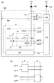
図1は、第1実施形態に係る記録装置100の全体構成例を示している。記録装置100は、電子写真方式の記録装置(例えばレーザープリンタ)である。記録装置100は、例えば、発光素子110、受光素子120、発光素子駆動用基板200および感光ドラム300を備える。基板200は、例えば、判定部130、駆動部140、電流生成部150、電流‐電流変換部160および制御部170を含む。
(First Embodiment)
FIG. 1 shows an overall configuration example of the
発光素子110は、アノードが、電源電圧VCCが伝搬する電源ノードnVCCに接続され、且つ、カソードが、駆動部140に接続されるように配される。発光素子110は、例えばレーザーダイオードであり、駆動部140により駆動されることにより発光し、その発光光(レーザー光)を感光ドラム300に照射する。
The
受光素子120は、カソードが電源ノードnVCCに接続され、且つ、アノードが判定部130に接続されるように配される。受光素子120は、フォトダイオード等の光電変換素子であり、発光素子110の発光光を受けて、その光量に応じた値の電流Imをモニタ電流として出力する。具体的には、受光素子120は、APCを含む動作時において逆バイアス状態となっており、発光素子110の発光光により受光素子120で発生した電荷は、その量に応じた値のモニタ電流Imを形成する。
The light receiving
制御部170は、例えば、記録動作を制御するためのCPU、プロセッサ等であり、電流生成部150および電流‐電流変換部160を制御信号sig1及びsig2によりそれぞれ制御する。例えば、電流生成部150は、定電流である基準電流I1(第1電流)を生成し、制御部170からの制御信号sig1に応答して該生成された基準電流I1を電流‐電流変換部160に出力する。他の例では、電流生成部150は、制御信号sig1に応答して基準電流I1を生成し、該生成された基準電流I1を電流‐電流変換部160に出力してもよい。
The
電流‐電流変換部160は、電流生成部150と判定部130との間の経路に配され、電流生成部150から基準電流I1を受ける。そして、電流‐電流変換部160は、制御部170からの制御信号sig2に応じた比率を基準電流I1の値に乗じて得られた値の電流I2を参照電流(第2電流)として出力する。電流‐電流変換部160は、単に「変換部」と称されてもよい。また、参照電流I2は、発光素子110の発光量の目標値に対応し、「ターゲット電流」と称されてもよい。なお、詳細は後述するが、制御信号sig2は複数の信号を含みうる。
The current-
判定部130は、受光素子120および電流‐電流変換部160に接続されており、モニタ電流Imと参照電流I2とに基づいて、発光素子110の発光量が目標値に達したか否かを判定する。詳細は後述とするが、判定部130は、例えば比較器を含み、該比較器によりモニタ電流Imと参照電流I2との比較を行い、その比較結果に基づいて、発光素子110の発光量が目標値に達したか否かを判定する。
The
駆動部140は、上記比較結果に基づいて発光素子110を駆動する。具体的には、駆動部140は、例えば、情報保持部(例えばサンプリング回路)とドライバとを含む(ともに不図示)。そして、駆動部140は、APC完了時の判定部130からの出力を、発光素子110の発光量を目標値にするため情報として情報保持部に保持する。ドライバは、その後の記録の際に、情報保持部に保持された情報に応じた駆動信号を用いて発光素子110を駆動する。
The
即ち、発光素子110、受光素子120、判定部130、駆動部140、電流生成部150および電流‐電流変換部160は、発光素子110の発光量を目標値に近付けるためのフィードバック系を形成しており、このような構成によりAPCが実現される。なお、ここではアノード駆動型のレーザーの構成例を示したが、カソード駆動型の構成にしてもよい。
That is, the
図2(a)は、記録装置100の構成例をより具体的に示している。基板200は、端子T1〜T3(電極パッド)を備える。第1端子T1は、発光素子110に接続され、駆動部140は、端子T1を介して発光素子110を駆動する。第2端子T2は、受光素子120に接続され、基板200は、端子T2を介してモニタ電流Imを受ける。第3端子T3は、定電圧である参照電圧Vrefを受ける。
FIG. 2A shows more concretely a configuration example of the
電流‐電流変換部160は、例えば、トランジスタM10〜13及びM20〜23により形成されるカレントミラー回路を含み、制御信号sig2(具体的には、制御信号sig21A、21B、22A及び22B)により制御される。これらトランジスタM10等には、例えばNMOSトランジスタが用いられうる。トランジスタM10〜13は、第1のカレントミラー回路161を形成しており、また、トランジスタM20〜23は、第2のカレントミラー回路162を形成している。
The current-
ここで、電流生成部150からの基準電流I1が流れるノードをノードn1とする。接地ノードをノードn2とする。ノードn1とノードn2との間に位置するノードをノードn3とする。ノードn1とノードn2との間に位置するノードであってノードn3とは異なる他のノードをノードn4とする。また、参照電流I2が流れるノードであって電流‐電流変換部160の出力端子に対応するノードをノードn5とする。
Here, the node through which the reference current I1 from the
カレントミラー回路161について、トランジスタM10は、ドレインがノードn1に接続され、ソースがノードn3に接続され、ゲートで制御信号sig21Aを受けるように配される。トランジスタM11は、ドレインおよびゲートがノードn3に接続され、ソースがノードn2に接続されるように配される。トランジスタM12は、ドレインがノードn5に接続され、ソースがノードn2に接続され、ゲートがノードn3に接続されるように配される。トランジスタM12は、トランジスタM11に流れる基準電流I1の値に、トランジスタM11とトランジスタM12とのサイズ比を乗じた値(第1の電流値)の参照電流I2を流す。以下では、区別のため、この参照電流I2を「参照電流I21」と記載する場合がある。トランジスタM13は、カレントミラー回路161がノンアクティブのときのノードn3の電位をLに固定するためのトランジスタであり、ドレインがノードn3に接続され、ソースがノードn2に接続され、ゲートで制御信号sig21Bを受けるように配される。 For the current mirror circuit 161 the transistor M10 is arranged such that the drain is connected to the node n1, the source is connected to the node n3, and the gate receives the control signal sig21A. The transistor M11 is arranged so that the drain and the gate are connected to the node n3 and the source is connected to the node n2. The transistor M12 is arranged such that the drain is connected to the node n5, the source is connected to the node n2, and the gate is connected to the node n3. The transistor M12 passes a reference current I2 having a value (first current value) obtained by multiplying the value of the reference current I1 flowing through the transistor M11 by the size ratio of the transistor M11 and the transistor M12. In the following, for the sake of distinction, this reference current I2 may be referred to as "reference current I21". The transistor M13 is a transistor for fixing the potential of the node n3 to L when the current mirror circuit 161 is inactive, the drain is connected to the node n3, the source is connected to the node n2, and the control signal sig21B is connected at the gate. Arranged to receive.
カレントミラー回路162について、トランジスタM20は、ドレインがノードn1に接続され、ソースがノードn4に接続され、ゲートで制御信号sig22Aを受けるように配される。トランジスタM21は、ドレインおよびゲートがノードn4に接続され、ソースがノードn2に接続されるように配される。トランジスタM22は、ドレインがノードn5に接続され、ソースがノードn2に接続され、ゲートがノードn4に接続されるように配される。トランジスタM22は、トランジスタM21に流れる基準電流I1の値に、トランジスタM21とトランジスタM22とのサイズ比を乗じた値(第2の電流値)の参照電流I2を流す。以下では、区別のため、この参照電流I2を「参照電流I22」と記載する場合がある。トランジスタM23は、カレントミラー回路162がノンアクティブのときのノードn4の電位をLに固定するためのトランジスタであり、ドレインがノードn4に接続され、ソースがノードn2に接続され、ゲートで制御信号sig22Bを受けるように配される。 For the current mirror circuit 162, the transistor M20 is arranged so that the drain is connected to the node n1, the source is connected to the node n4, and the control signal sig22A is received at the gate. The transistor M21 is arranged so that the drain and the gate are connected to the node n4 and the source is connected to the node n2. The transistor M22 is arranged such that the drain is connected to the node n5, the source is connected to the node n2, and the gate is connected to the node n4. The transistor M22 passes a reference current I2 having a value (second current value) obtained by multiplying the value of the reference current I1 flowing through the transistor M21 by the size ratio of the transistor M21 and the transistor M22. In the following, for the sake of distinction, this reference current I2 may be referred to as "reference current I22". The transistor M23 is a transistor for fixing the potential of the node n4 to L when the current mirror circuit 162 is inactive, the drain is connected to the node n4, the source is connected to the node n2, and the control signal sig22B is connected at the gate. Arranged to receive.
トランジスタM11とトランジスタM12とのサイズ比は、電流‐電流変換部160の電流変換率に対応し、カレントミラー回路161の「ミラー比」とも表現されうる。トランジスタM21とトランジスタM22とのサイズ比についても同様である。
The size ratio of the transistor M11 and the transistor M12 corresponds to the current conversion rate of the current-
図2(b)は、電流‐電流変換部160の動作タイミングチャートを示している。本構成例によると、電流‐電流変換部160は、制御信号sig21A、21B、22A及び22Bに応じた比率を基準電流I1の値に乗じて得られた値の参照電流I21又はI22を出力する。例えば、制御信号sig21A及びsig22BがH(ハイレベル)、且つ、制御信号sig21B及びsig22AがL(ローレベル)の期間P1では、カレントミラー回路161はアクティブとなり、カレントミラー回路162はノンアクティブとなる。期間P1では、ノードn5には、第1の電流値の参照電流I21が流れる。一方、制御信号sig21A及びsig22BがL、且つ、制御信号sig21B及びsig22AがHの期間P2では、カレントミラー回路161はノンアクティブとなり、カレントミラー回路162はアクティブとなる。期間P2では、ノードn5には、第2の電流値の参照電流I22が流れる。
FIG. 2B shows an operation timing chart of the current-
即ち、電流‐電流変換部160は、制御信号sig2に基づいて、カレントミラー回路161及び162の一方がアクティブになることにより、参照電流I2(参照電流I21及びI22の一方)を出力することができる。1回のAPCを行っている間(即ち、APCを開始してから発光素子110の発光量が目標値になるまでの間)、制御信号sig1及びsig2の論理レベルは固定され、参照電流I2の値は固定される。
That is, the current-
再び、図2(a)を参照すると、判定部130は、例えば、反転入力端子INN(図中において「−」で示された第1入力端子)および非反転入力端子INP(図中において「+」で示された第2入力端子)を有する比較器を含む。反転入力端子INNと、受光素子120のアノードと、ノードn5とは、互いに接続されており(例えば、配線パターン、コンタクトプラグ等の導電部材により互いに接続されており)、実質的に互いに同電位である。非反転入力端子INPは、端子T3を介して参照電圧Vrefを受ける。
With reference to FIG. 2A again, the
参照電圧Vrefは、例えば、電源電圧VCCと、接地用の電圧(ノードn2の電圧)VSSとの間の電圧であって、カレントミラー回路161(又は162)が参照電流I21(又はI22)を適切に出力することが可能となる範囲内の電圧であればよい。具体的には、参照電圧Vrefは、カレントミラー回路161及び162を構成するトランジスタM11等がソースフォロワ動作を行うことが可能な範囲内の電圧であればよい。 The reference voltage Vref is, for example, a voltage between the power supply voltage VCS and the grounding voltage (voltage of node n2) VSS, and the current mirror circuit 161 (or 162) appropriately adjusts the reference current I21 (or I22). The voltage may be within the range that can be output to. Specifically, the reference voltage Vref may be a voltage within a range in which the transistors M11 and the like constituting the current mirror circuits 161 and 162 can perform the source follower operation.
例えば、受光素子120のモニタ電流Imの電流値が、参照電流I2(I21又はI22)の電流値よりも大きいとき(即ち、発光素子110の発光量が目標値より大きいとき)、反転入力端子INNの電位は上がって参照電圧Vrefより高くなる。このことは、モニタ電流Imと参照電流I2(<Im)との差分(Im−I2)により、反転入力端子INNの入力容量が充電されると考えればよい。他の観点では、受光素子120で生じる単位時間あたりの電荷量が参照電流I2よりも大きいことによって受光素子120では電荷が増加し、該増加する電荷が反転入力端子INNの電位を上げる、と考えてもよい。そして、駆動部140は、このときの判定部130の比較器の出力を受けて、発光素子110を駆動するための駆動力を下げる。
For example, when the current value of the monitor current Im of the
一方、モニタ電流Imの電流値が参照電流I2の電流値よりも小さいとき(即ち、発光素子110の発光量が目標値より小さいとき)、反転入力端子INNの電位は下がって参照電圧Vrefより低くなる。このことは、モニタ電流Imと参照電流I2(>Im)との差分(I2−Im)により、反転入力端子INNの入力容量からの放電が生じると考えればよい。他の観点では、受光素子120で生じる単位時間あたりの電荷量が参照電流I2よりも小さいことによって受光素子120では電荷が減少し、該減少する電荷が反転入力端子INNの電位を下げる、と考えてもよい。そして、駆動部140は、このときの判定部130の比較器の出力を受けて、発光素子110を駆動するための駆動力を上げる。
On the other hand, when the current value of the monitor current Im is smaller than the current value of the reference current I2 (that is, when the amount of light emitted by the
本実施形態では、判定部130は、このような構成によりモニタ電流Imと参照電流I2との比較を行い、その比較結果に基づいて、発光素子110の発光量を目標値にするためのフィードバック制御が為される。このフィードバック制御によりAPCが実現される。モニタ電流Imの電流値と参照電流I2の電流値とが互いに等しくなったとき、反転入力端子INNの電位は、参照電圧Vrefと同電位になる。このような状態になったときに、発光素子110の発光量が目標値になったと判定されてもよい。なお、フィードバック制御においては、必ずしも反転入力端子INNの電位と参照電圧Vrefとを同電位にする必要はなく、モニタ電流Imと参照電流I2との比較結果に応じて発光素子110の発行量を変化させればよい。
In the present embodiment, the
制御部170は電流‐電流変換部160を制御する。具体的には、制御部170は、カレントミラー回路161及び162の一方をアクティブにして電流‐電流変換部160の電流変換比率(「ゲイン」と称されてもよい。)を制御し、参照電流I2(I21又はI22)を出力させる。例えば、制御部170は、不図示の計測部を含み、該計測部によって感光ドラム300の使用量(回転回数、劣化の程度等)を計測し、その計測結果に基づく制御信号sig2を用いて電流‐電流変換部160を制御してもよい。
The
以上、本構成例によると、電流‐電流変換部160は、電流生成部150と判定部130との間の経路に配され、電流生成部150からの基準電流I1を制御信号sig2に基づいて変換(又は変調)し、参照電流I21及びI22の一方を出力する。電流‐電流変換部160の電流変換率は、制御信号sig2によって定まり、例えばAPCのたびに適切に調整されてもよい(例えば、感光ドラム300の使用量に応じてAPCが為されてもよい。)。これにより、対応する目標値に発光素子110の発光量を近付けることができる。本構成例によると、処理対象がモニタ電流Imではなく基準電流I1であり、受光素子120と判定部130との間の経路に他の電流‐電流変換器が配置する必要がない。よって、本構成例によると、モニタ電流Imの判定部130へのフィードバック遅延を防ぐのに有利である。
As described above, according to this configuration example, the current-
特に、本構成例によると、電流‐電流変換部160の電流変換率が変更された場合のフィードバック遅延の変動量が、電流変換率の変更が可能な他の電流‐電流変換器が受光素子120と判定部130との間に配置された場合に比べて抑制されうる。このことは、動作周波数帯域が変わることによるフィードバック系の発振等を防ぎ、APCを安定化させるのに有利である。なお、他の例では、受光素子120と判定部130との間に他の電流‐電流変換器が配されてもよい(即ち、モニタ電流Imに対して変換処理が為されてもよい)が、この場合、モニタ電流Imおよび基準電流I1の双方についての電流変換率を調整することにより、APCを安定化させるとよい。
In particular, according to this configuration example, the fluctuation amount of the feedback delay when the current conversion rate of the current-
また、ここでは電流‐電流変換部160が2つの参照電流I21及びI22の一方を出力する態様を例示したが、電流‐電流変換部160は、互いに電流値が異なる3以上の参照電流の1つを出力してもよい。この場合、電流‐電流変換部160は、3以上のカレントミラー回路を含み、それらの1つをアクティブにすることによって上記3以上の参照電流の1つを出力するように構成されてもよい。他の例では、電流‐電流変換部160は、複数のカレントミラー回路の少なくとも1つ(2以上でも可)をアクティブにすることによって互いに電流値が異なる複数の参照電流の1つを出力するように構成されてもよい。
Further, although the mode in which the current-
(第2実施形態)
図3を参照しながら第2実施形態を述べる。本実施形態は、発光素子110と判定部130と駆動部140とが単位グループGを形成しており、基板200がグループGを複数有する、という点で前述の第1実施形態と異なる。ここでは説明を容易にするため、グループの数を2とし、また、区別のため、該2つのグループGをそれぞれ「グループGa」、「グループGb」とする。図3に例示されるように、基準電流生成部150および電流‐電流変換部160は、グループGa及びGbのそれぞれに対応して配されうる。
(Second Embodiment)
The second embodiment will be described with reference to FIG. This embodiment is different from the above-described first embodiment in that the
なお、図中において、上記発光素子110等の各素子ないし各ユニットがグループGa及びGbのいずれのものであるか区別するため、各素子ないし各ユニットの符号を「a」又は「b」を付して示す。例えば、グループGaの発光素子110を「発光素子110a」と示す(他の素子ないしユニットについても同様である。)。
In the figure, in order to distinguish whether each element or unit such as the
また、グループGa及びGbは、例えば、カラー印刷対応の記録装置100において、互いに異なるカラーに対応する。そのため、グループの数は、カラーの数に対応する。例えば、Y(イエロー)、M(マゼンダ)、C(シアン)、K(ブラック)の4色対応の場合、グループGの数を4にしてもよいし、他の例では、2つのグループGを有する基板200を2つ準備してもよい。
Further, the groups Ga and Gb correspond to different colors from each other in, for example, the
図3によると、比較部130a及び130bの双方と受光素子120との間の経路には、スイッチ部USWが配されており、スイッチ部USWは、受光素子120を、比較部130a及び130bの一方に接続する。このような構成によると、スイッチ部USWを制御することにより、グループGaについてのAPCと、グループGbについてのAPCとを順に行うことができる。具体的には、例えば、スイッチ部USWは、受光素子120と比較部130aとを電気的に接続し、グループGaについてのAPCにより発光素子110aの発光量が調節された後、受光素子120と比較部130bとを電気的に接続する。
According to FIG. 3, a switch unit USW is arranged in the path between both the
本実施形態によると、発光素子110と判定部130と駆動部140とにより形成されるグループGを複数有する記録装置100(例えばカラー印刷対応の記録装置100)においても、第1実施形態と同様の効果が得られる。
According to the present embodiment, the recording device 100 (for example, the
(その他)
以上、いくつかの好適な実施形態を例示したが、本発明はこれらに限られるものではなく、本発明の趣旨を逸脱しない範囲で、その一部が変更されてもよい。
(Other)
Although some preferred embodiments have been illustrated above, the present invention is not limited to these, and some of them may be modified without departing from the spirit of the present invention.
100:記録装置、110:発光素子、120:受光素子、130:判定部、140:駆動部、150:電流生成部、160:電流‐電流変換部、170:制御部。 100: Recording device, 110: Light emitting element, 120: Light receiving element, 130: Judgment unit, 140: Drive unit, 150: Current generation unit, 160: Current-current conversion unit, 170: Control unit.
Claims (17)
前記発光素子の発光量に応じた値を有するモニタ電流を出力する出力端子を有する受光素子と、
第1入力端子および第2入力端子を有し、前記第1入力端子の電圧と前記第2入力端子の電圧とを比較する比較部と、
前記比較部による比較結果に基づいて前記発光素子を駆動する駆動部と、
第1電流値を有する第1電流を生成する電流生成部と、
前記第1電流を受ける入力端子、制御信号を受ける入力端子、および、参照電流として第2電流値を有する第2電流を出力する出力端子を有する変換部と、を備え、
前記第1電流値に対する前記第2電流値の比率は、前記制御信号に応じて設定され、
前記受光素子の前記出力端子、前記変換部の前記出力端子、および、前記比較部の前記第1入力端子は、相互に接続され、前記第2入力端子は、参照電圧を受け、
前記駆動部は前記第1入力端子の電圧と前記第2入力端子の電圧とが同電位になるように前記発光素子を駆動する、
ことを特徴とする記録装置。 Light emitting element and
A light receiving element having an output terminal for outputting a monitor current having a value corresponding to the amount of light emitted from the light emitting element, and a light receiving element.
A comparison unit having a first input terminal and a second input terminal and comparing the voltage of the first input terminal with the voltage of the second input terminal.
A drive unit that drives the light emitting element based on the comparison result by the comparison unit,
A current generator that generates a first current having a first current value,
Input terminal for receiving the first current input terminal for receiving a control signal, and, and a conversion unit having an output terminal for outputting a second current having a second current value as referenced current,
The ratio of the second current value to the first current value is set according to the control signal.
Said output terminal of said light receiving element, the output terminal of the conversion unit, and the first input terminal of the comparison unit is connected to each other, said second input terminal, receiving the reference voltage,
The drive unit drives the light emitting element so that the voltage of the first input terminal and the voltage of the second input terminal have the same potential.
A recording device characterized by that.
前記発光素子の発光量に応じた値を有するモニタ電流を出力する受光素子と、
前記受光素子に接続され、前記モニタ電流と参照電流との大小関係に応じた電圧と参照電圧とを比較する比較部と、
前記比較部による比較結果に基づいて前記発光素子を駆動する駆動部と、
第1電流値を有する第1電流を生成する電流生成部と、
前記電流生成部と前記比較部との間の経路に配され、制御信号を受けて、前記参照電流として第2電流値を有する第2電流を出力する変換部と、を備え、
前記第1電流値に対する前記第2電流値の比率は、前記制御信号に応じて設定され、
前記変換部は、それぞれが前記第1電流を受ける少なくとも2つのカレントミラー回路を含み、
前記比較部は、第1入力端子および第2入力端子を含み、
前記受光素子の前記モニタ電流を出力する出力端子、前記変換部の前記参照電流を出力する出力端子、および、前記第1入力端子は、相互に接続され、
前記第2入力端子は、前記参照電圧を受け、
前記駆動部は前記モニタ電流と参照電流との大小関係に応じた電圧と前記参照電圧とが同電位になるように前記発光素子を駆動する、
ことを特徴とする記録装置。 Light emitting element and
A light receiving element that outputs a monitor current having a value corresponding to the amount of light emitted from the light emitting element, and a light receiving element.
A comparison unit connected to the light receiving element and comparing a voltage and a reference voltage according to the magnitude relationship between the monitor current and the reference current.
A drive unit that drives the light emitting element based on the comparison result by the comparison unit,
A current generator that generates a first current having a first current value,
It is provided with a conversion unit which is arranged in a path between the current generation unit and the comparison unit, receives a control signal, and outputs a second current having a second current value as the reference current.
The ratio of the second current value to the first current value is set according to the control signal.
The converter includes at least two current mirror circuits, each of which receives the first current.
The comparison unit includes a first input terminal and a second input terminal.
The output terminal that outputs the monitor current of the light receiving element, the output terminal that outputs the reference current of the conversion unit, and the first input terminal are connected to each other.
It said second input terminal, receiving the reference voltage,
The drive unit drives the light emitting element so that the voltage corresponding to the magnitude relationship between the monitor current and the reference current and the reference voltage have the same potential.
A recording device characterized by that.
ことを特徴とする請求項2に記載の記録装置。 Each of the at least two current mirror circuits becomes active based on the control signal.
2. The recording device according to claim 2.
前記制御信号は、前記スイッチをオンまたはオフする、
ことを特徴とする請求項3に記載の記録装置。 The conversion unit includes a switch that connects the current generation unit and one of the at least two current mirror circuits.
The control signal turns the switch on or off.
The recording device according to claim 3, wherein the recording device is characterized by the above.
ことを特徴とする請求項4に記載の記録装置。 The comparison unit includes a first input terminal, and each of the output terminals of the at least two current mirror circuits is connected to the first input terminal.
The recording device according to claim 4.
ことを特徴とする請求項5に記載の記録装置。 At least two of the at least two current mirror circuits have different mirror ratios from each other.
The recording device according to claim 5.
前記複数のグループの1つの前記比較部を前記受光素子に選択的に接続する選択スイッチと、
を更に備える、
ことを特徴とする請求項1乃至6のいずれか1項に記載の記録装置。 A plurality of groups, each of which includes the light emitting element, the comparison unit, and the drive unit,
A selection switch that selectively connects one of the plurality of groups to the light receiving element,
Further prepare
The recording device according to any one of claims 1 to 6, wherein the recording device is characterized by the above.
前記感光ドラムの使用量に応じた信号を前記制御信号として用いて前記変換部を制御する制御部と、をさらに備える
ことを特徴とする請求項1乃至7のいずれか1項に記載の記録装置。 A photosensitive drum that receives light from the light emitting element and
The recording device according to any one of claims 1 to 7, further comprising a control unit that controls the conversion unit by using a signal corresponding to the amount of the photosensitive drum used as the control signal. ..
前記発光素子の発光量に応じた値を有するモニタ電流を出力する出力端子を有する受光素子と、
第1電流値を有する第1電流を生成する電流生成部と、
制御信号および前記第1電流を受けて、参照電流として第2電流値を有する第2電流を出力する出力端子を有する変換部と、
前記受光素子の前記出力端子および前記変換部の前記出力端子の双方に接続された第1入力端子、および、参照電圧を受ける第2入力端子を有する比較部と、
前記比較部からの出力に基づいて前記発光素子を駆動する駆動部と、を備え、
前記第1電流値に対する前記第2電流値の比率は、前記制御信号に応じて設定されており、
前記駆動部は前記第1入力端子の電圧と前記第2入力端子の電圧とが同電位になるように前記発光素子を駆動する、
ことを特徴とする記録装置。 Light emitting element and
A light receiving element having an output terminal for outputting a monitor current having a value corresponding to the amount of light emitted from the light emitting element, and a light receiving element.
A current generator that generates a first current having a first current value,
A conversion unit having an output terminal that receives a control signal and the first current and outputs a second current having a second current value as a reference current.
A comparison unit having a first input terminal connected to both the output terminal of the light receiving element and the output terminal of the conversion unit, and a second input terminal that receives a reference voltage.
A drive unit that drives the light emitting element based on the output from the comparison unit is provided.
The ratio of the second current value to the first current value is set in response to the control signal,
The drive unit drives the light emitting element so that the voltage of the first input terminal and the voltage of the second input terminal have the same potential.
A recording device characterized by that.
受光素子からのモニタ電流を受けるための第2端子と、
第1入力端子および第2入力端子を有し、前記第1入力端子の電圧と前記第2入力端子の電圧とを比較する比較部と、
前記比較部による比較結果に基づいて前記第1端子へ前記駆動信号を出力する駆動部と、
第1電流値を有する第1電流を生成する電流生成部と、
前記第1電流を受ける入力端子、制御信号を受ける入力端子、および、参照電流として第2電流値を有する第2電流を出力する出力端子を有する変換部と、を備え、
前記第1電流値に対する前記第2電流値の比率は、前記制御信号に応じて設定され、
前記受光素子の前記出力端子、前記変換部の前記出力端子、および、前記比較部の前記第1入力端子は、相互に接続され、前記第2入力端子は、参照電圧を受け、
前記駆動部は前記第1入力端子の電圧と前記第2入力端子の電圧とが同電位になるように前記発光素子を駆動する、
ことを特徴とする発光素子駆動用基板。 The first terminal for outputting the drive signal for driving the light emitting element, and
The second terminal for receiving the monitor current from the light receiving element,
A comparison unit having a first input terminal and a second input terminal and comparing the voltage of the first input terminal with the voltage of the second input terminal.
A drive unit that outputs the drive signal to the first terminal based on the comparison result by the comparison unit, and a drive unit.
A current generator that generates a first current having a first current value,
Input terminal for receiving the first current input terminal for receiving a control signal, and, and a conversion unit having an output terminal for outputting a second current having a second current value as referenced current,
The ratio of the second current value to the first current value is set according to the control signal.
Said output terminal of said light receiving element, the output terminal of the conversion unit, and the first input terminal of the comparison unit is connected to each other, said second input terminal, receiving the reference voltage,
The drive unit drives the light emitting element so that the voltage of the first input terminal and the voltage of the second input terminal have the same potential.
A substrate for driving a light emitting element.
前記発光素子の発光量に応じた値を有するモニタ電流を出力する受光素子と、
第1電流値を有する第1電流を生成する電流生成部と、
制御信号および前記第1電流を受けて、参照電流として第2電流値を有する第2電流を出力する変換部と、
前記受光素子の前記モニタ電流を出力する出力端子、および、前記変換部の前記参照電流を出力する出力端子の双方に接続された第1入力端子、および、参照電圧を受ける第2入力端子を有する比較部と、
前記比較部による比較結果に基づいて前記発光素子を駆動する駆動部と、を備え、
前記第1電流値に対する前記第2電流値の比率は、前記制御信号に応じて設定され、
前記変換部は、それぞれが前記第1電流を受ける少なくとも2つのカレントミラー回路を含み、
前記駆動部は前記第1入力端子の電圧と前記第2入力端子の電圧とが同電位になるように前記発光素子を駆動する、
ことを特徴とする記録装置。 Light emitting element and
A light receiving element that outputs a monitor current having a value corresponding to the amount of light emitted from the light emitting element, and a light receiving element.
A current generator that generates a first current having a first current value,
A conversion unit that receives a control signal and the first current and outputs a second current having a second current value as a reference current.
It has a first input terminal connected to both an output terminal that outputs the monitor current of the light receiving element and an output terminal that outputs the reference current of the conversion unit, and a second input terminal that receives a reference voltage. Comparison part and
A drive unit that drives the light emitting element based on the comparison result by the comparison unit is provided.
The ratio of the second current value to the first current value is set according to the control signal.
The converting unit, viewed contains at least two current mirror circuits, respectively receiving the first current,
The drive unit drives the light emitting element so that the voltage of the first input terminal and the voltage of the second input terminal have the same potential.
A recording device characterized by that.
ことを特徴とする請求項11に記載の記録装置。 Each of the at least two current mirror circuits becomes active based on the control signal.
The recording device according to claim 11.
前記制御信号は、前記スイッチをオンまたはオフする、
ことを特徴とする請求項12に記載の記録装置。 The conversion unit includes a switch that connects the current generation unit and one of the at least two current mirror circuits.
The control signal turns the switch on or off.
The recording device according to claim 12.
ことを特徴とする請求項13に記載の記録装置。 The comparison unit includes a first input terminal, and each of the output terminals of the at least two current mirror circuits is connected to the first input terminal.
13. The recording device according to claim 13.
ことを特徴とする請求項14に記載の記録装置。 At least two of the at least two current mirror circuits have different mirror ratios from each other.
14. The recording device according to claim 14.
前記受光素子の前記モニタ電流を出力する前記出力端子、前記変換部の前記参照電流を出力する前記出力端子、および、前記第1入力端子は、相互に接続され、
前記第2入力端子は、参照電圧を受ける、
ことを特徴とする請求項15に記載の記録装置。 The comparison unit includes a first input terminal and a second input terminal.
The output terminal that outputs the monitor current of the light receiving element, the output terminal that outputs the reference current of the conversion unit, and the first input terminal are connected to each other.
The second input terminal receives a reference voltage.
The recording device according to claim 15.
前記複数のグループの1つの前記比較部を前記受光素子に選択的に接続する選択スイッチと、
を更に備える、
ことを特徴とする請求項10に記載の発光素子駆動用基板。 A plurality of groups, each of which includes the light emitting element, the comparison unit, and the drive unit,
A selection switch that selectively connects one of the plurality of groups to the light receiving element,
Further prepare
The light emitting element driving substrate according to claim 10.
Priority Applications (2)
| Application Number | Priority Date | Filing Date | Title |
|---|---|---|---|
| JP2015187439A JP6886235B2 (en) | 2015-09-24 | 2015-09-24 | Recording device and light emitting element drive substrate |
| US15/254,851 US10025219B2 (en) | 2015-09-24 | 2016-09-01 | Printing apparatus and substrate for driving light-emitting element |
Applications Claiming Priority (1)
| Application Number | Priority Date | Filing Date | Title |
|---|---|---|---|
| JP2015187439A JP6886235B2 (en) | 2015-09-24 | 2015-09-24 | Recording device and light emitting element drive substrate |
Publications (3)
| Publication Number | Publication Date |
|---|---|
| JP2017063110A JP2017063110A (en) | 2017-03-30 |
| JP2017063110A5 JP2017063110A5 (en) | 2018-10-04 |
| JP6886235B2 true JP6886235B2 (en) | 2021-06-16 |
Family
ID=58409074
Family Applications (1)
| Application Number | Title | Priority Date | Filing Date |
|---|---|---|---|
| JP2015187439A Active JP6886235B2 (en) | 2015-09-24 | 2015-09-24 | Recording device and light emitting element drive substrate |
Country Status (2)
| Country | Link |
|---|---|
| US (1) | US10025219B2 (en) |
| JP (1) | JP6886235B2 (en) |
Families Citing this family (1)
| Publication number | Priority date | Publication date | Assignee | Title |
|---|---|---|---|---|
| JP7154079B2 (en) | 2018-09-14 | 2022-10-17 | キヤノン株式会社 | Substrate for driving recording device and light-emitting element |
Family Cites Families (19)
| Publication number | Priority date | Publication date | Assignee | Title |
|---|---|---|---|---|
| JPS6376493A (en) * | 1986-09-19 | 1988-04-06 | Toshiba Corp | Laser diode drive circuit |
| JP2840275B2 (en) * | 1989-02-03 | 1998-12-24 | 株式会社リコー | Semiconductor laser controller |
| DE69132464T2 (en) | 1990-07-05 | 2001-05-10 | Canon Kk | Imaging device and associated switching device for constant current switching |
| JPH11348344A (en) * | 1998-06-04 | 1999-12-21 | Hitachi Koki Co Ltd | Semiconductor laser control apparatus of electrophotographic apparatus |
| US6392215B1 (en) * | 1999-09-20 | 2002-05-21 | International Business Machines Corporation | Laser diode driving circuit |
| JP3785020B2 (en) * | 2000-03-24 | 2006-06-14 | 株式会社東芝 | Semiconductor laser drive circuit |
| JP4283454B2 (en) * | 2001-03-09 | 2009-06-24 | 株式会社リコー | Semiconductor laser control apparatus and method |
| JP2002337385A (en) * | 2001-05-16 | 2002-11-27 | Ricoh Co Ltd | Laser diode controller |
| JP4572503B2 (en) * | 2003-03-20 | 2010-11-04 | 富士ゼロックス株式会社 | Light emitting element driving device and light emitting system |
| JP2006060751A (en) * | 2004-08-24 | 2006-03-02 | Ricoh Co Ltd | Output device, differential output device, semiconductor laser modulation driving apparatus, image forming apparatus and electronic equipment |
| KR100790134B1 (en) * | 2006-04-26 | 2008-01-02 | 삼성전자주식회사 | Structure of Driving for a Sequential RGB Display |
| JP2011187494A (en) * | 2010-03-04 | 2011-09-22 | Ricoh Co Ltd | Semiconductor laser-driving device and image forming device equipped with the same |
| JP5357118B2 (en) | 2010-08-09 | 2013-12-04 | 旭化成エレクトロニクス株式会社 | Semiconductor laser drive control circuit |
| CN101924324B (en) * | 2010-09-07 | 2012-05-23 | 凯钰科技股份有限公司 | Automatic power control circuit for controlling bias current of laser diode |
| JP2013156520A (en) * | 2012-01-31 | 2013-08-15 | Konica Minolta Inc | Image formation device |
| JP6238560B2 (en) * | 2012-06-08 | 2017-11-29 | キヤノン株式会社 | Image forming apparatus |
| JP6061505B2 (en) * | 2012-06-08 | 2017-01-18 | キヤノン株式会社 | Optical scanning apparatus and image forming apparatus having the same |
| JP6003431B2 (en) * | 2012-09-12 | 2016-10-05 | 富士ゼロックス株式会社 | Light amount control apparatus, exposure apparatus, and image forming apparatus |
| JP6442318B2 (en) | 2015-02-12 | 2018-12-19 | キヤノン株式会社 | DRIVE CIRCUIT FOR RECORDING DEVICE, LIGHT EMITTING ELEMENT UNIT, AND RECORDING DEVICE |
-
2015
- 2015-09-24 JP JP2015187439A patent/JP6886235B2/en active Active
-
2016
- 2016-09-01 US US15/254,851 patent/US10025219B2/en active Active
Also Published As
| Publication number | Publication date |
|---|---|
| US10025219B2 (en) | 2018-07-17 |
| JP2017063110A (en) | 2017-03-30 |
| US20170090336A1 (en) | 2017-03-30 |
Similar Documents
| Publication | Publication Date | Title |
|---|---|---|
| US8957934B2 (en) | Light source drive circuit, optical scanning apparatus, semiconductor drive circuit, and image forming apparatus | |
| US8896648B2 (en) | Laser driving unit and image forming apparatus | |
| JP5471569B2 (en) | Laser driving device, optical scanning device, image forming apparatus, and laser driving method | |
| JP2011066089A (en) | Semiconductor laser control device, and image formation device | |
| US8059146B2 (en) | Exposure device, image forming apparatus, and computer-readable medium | |
| JP6886235B2 (en) | Recording device and light emitting element drive substrate | |
| US10462862B2 (en) | Light source control device and image forming apparatus | |
| US9575432B2 (en) | Image forming apparatus | |
| JP2014107461A (en) | Semiconductor laser driving circuit and image forming apparatus | |
| JP6442318B2 (en) | DRIVE CIRCUIT FOR RECORDING DEVICE, LIGHT EMITTING ELEMENT UNIT, AND RECORDING DEVICE | |
| US8259770B2 (en) | Laser array | |
| JP2008233115A (en) | Light quantity controller, optical scanner, and image forming apparatus | |
| JP2002321402A (en) | Imaging apparatus | |
| JP5717402B2 (en) | Image forming apparatus | |
| JP7154079B2 (en) | Substrate for driving recording device and light-emitting element | |
| JP2000208864A (en) | Semiconductor laser drive device | |
| JP6602123B2 (en) | Image forming apparatus | |
| JP6741460B2 (en) | Laser drive device and laser printer | |
| JP2000187374A (en) | Image forming device | |
| JP2008227129A (en) | Semiconductor laser controller, optical scanner, and image forming device | |
| JP2000307356A (en) | Negative feedback control circuit, light emitting means driving circuit, semiconductor laser driving circuit and electronic photographic device | |
| JP2017039281A (en) | Image forming apparatus | |
| JPH04356986A (en) | Laser recorder | |
| JP2007079501A (en) | Light emission control circuit, image formation featured value detection circuit utilizing the circuit and image forming apparatus provided with the circuit | |
| JP2002270950A (en) | Semiconductor laser driving method |
Legal Events
| Date | Code | Title | Description |
|---|---|---|---|
| A521 | Written amendment |
Free format text: JAPANESE INTERMEDIATE CODE: A523 Effective date: 20180822 |
|
| A621 | Written request for application examination |
Free format text: JAPANESE INTERMEDIATE CODE: A621 Effective date: 20180822 |
|
| A977 | Report on retrieval |
Free format text: JAPANESE INTERMEDIATE CODE: A971007 Effective date: 20190627 |
|
| A131 | Notification of reasons for refusal |
Free format text: JAPANESE INTERMEDIATE CODE: A131 Effective date: 20190716 |
|
| A521 | Written amendment |
Free format text: JAPANESE INTERMEDIATE CODE: A523 Effective date: 20190913 |
|
| A131 | Notification of reasons for refusal |
Free format text: JAPANESE INTERMEDIATE CODE: A131 Effective date: 20200217 |
|
| A521 | Written amendment |
Free format text: JAPANESE INTERMEDIATE CODE: A523 Effective date: 20200402 |
|
| A131 | Notification of reasons for refusal |
Free format text: JAPANESE INTERMEDIATE CODE: A131 Effective date: 20200911 |
|
| A521 | Written amendment |
Free format text: JAPANESE INTERMEDIATE CODE: A523 Effective date: 20201110 |
|
| RD01 | Notification of change of attorney |
Free format text: JAPANESE INTERMEDIATE CODE: A7421 Effective date: 20210103 |
|
| A521 | Written amendment |
Free format text: JAPANESE INTERMEDIATE CODE: A523 Effective date: 20210113 |
|
| TRDD | Decision of grant or rejection written | ||
| A01 | Written decision to grant a patent or to grant a registration (utility model) |
Free format text: JAPANESE INTERMEDIATE CODE: A01 Effective date: 20210416 |
|
| A61 | First payment of annual fees (during grant procedure) |
Free format text: JAPANESE INTERMEDIATE CODE: A61 Effective date: 20210514 |
|
| R151 | Written notification of patent or utility model registration |
Ref document number: 6886235 Country of ref document: JP Free format text: JAPANESE INTERMEDIATE CODE: R151 |