JP6060308B2 - インシトゥプロファイル制御(ispc)を用いた残留物クリアリングの動的制御 - Google Patents
インシトゥプロファイル制御(ispc)を用いた残留物クリアリングの動的制御 Download PDFInfo
- Publication number
- JP6060308B2 JP6060308B2 JP2016500309A JP2016500309A JP6060308B2 JP 6060308 B2 JP6060308 B2 JP 6060308B2 JP 2016500309 A JP2016500309 A JP 2016500309A JP 2016500309 A JP2016500309 A JP 2016500309A JP 6060308 B2 JP6060308 B2 JP 6060308B2
- Authority
- JP
- Japan
- Prior art keywords
- polishing
- substrate
- zone
- zones
- time
- Prior art date
- Legal status (The legal status is an assumption and is not a legal conclusion. Google has not performed a legal analysis and makes no representation as to the accuracy of the status listed.)
- Active
Links
- 238000011065 in-situ storage Methods 0.000 title claims description 13
- 239000000758 substrate Substances 0.000 claims description 355
- 238000005498 polishing Methods 0.000 claims description 348
- 238000001228 spectrum Methods 0.000 claims description 180
- 238000000034 method Methods 0.000 claims description 116
- 238000012886 linear function Methods 0.000 claims description 70
- 238000012544 monitoring process Methods 0.000 claims description 53
- 230000003287 optical effect Effects 0.000 claims description 44
- 239000000463 material Substances 0.000 claims description 36
- 238000004364 calculation method Methods 0.000 claims description 18
- 239000013590 bulk material Substances 0.000 claims description 15
- 238000012937 correction Methods 0.000 claims description 7
- 239000010410 layer Substances 0.000 description 56
- 230000008569 process Effects 0.000 description 46
- 238000007517 polishing process Methods 0.000 description 45
- 238000005259 measurement Methods 0.000 description 22
- 235000012431 wafers Nutrition 0.000 description 13
- 238000010586 diagram Methods 0.000 description 10
- 230000003595 spectral effect Effects 0.000 description 10
- 238000001514 detection method Methods 0.000 description 9
- 239000000126 substance Substances 0.000 description 9
- 238000012545 processing Methods 0.000 description 8
- 230000006870 function Effects 0.000 description 7
- 239000002002 slurry Substances 0.000 description 7
- 238000004590 computer program Methods 0.000 description 6
- 239000000203 mixture Substances 0.000 description 6
- RYGMFSIKBFXOCR-UHFFFAOYSA-N Copper Chemical compound [Cu] RYGMFSIKBFXOCR-UHFFFAOYSA-N 0.000 description 5
- 239000003989 dielectric material Substances 0.000 description 5
- 238000005070 sampling Methods 0.000 description 5
- 238000012360 testing method Methods 0.000 description 5
- 230000008859 change Effects 0.000 description 4
- 229910052802 copper Inorganic materials 0.000 description 4
- 239000010949 copper Substances 0.000 description 4
- 230000007423 decrease Effects 0.000 description 4
- 238000000151 deposition Methods 0.000 description 4
- 239000000945 filler Substances 0.000 description 4
- 239000007787 solid Substances 0.000 description 4
- 229910052581 Si3N4 Inorganic materials 0.000 description 3
- VYPSYNLAJGMNEJ-UHFFFAOYSA-N Silicium dioxide Chemical compound O=[Si]=O VYPSYNLAJGMNEJ-UHFFFAOYSA-N 0.000 description 3
- 230000004888 barrier function Effects 0.000 description 3
- 238000004422 calculation algorithm Methods 0.000 description 3
- 238000012625 in-situ measurement Methods 0.000 description 3
- 239000012528 membrane Substances 0.000 description 3
- 239000013307 optical fiber Substances 0.000 description 3
- HQVNEWCFYHHQES-UHFFFAOYSA-N silicon nitride Chemical compound N12[Si]34N5[Si]62N3[Si]51N64 HQVNEWCFYHHQES-UHFFFAOYSA-N 0.000 description 3
- 229910052814 silicon oxide Inorganic materials 0.000 description 3
- 101100119135 Mus musculus Esrrb gene Proteins 0.000 description 2
- 101150107278 POLD1 gene Proteins 0.000 description 2
- 101150043219 POLD2 gene Proteins 0.000 description 2
- 230000007547 defect Effects 0.000 description 2
- 230000008021 deposition Effects 0.000 description 2
- 239000007788 liquid Substances 0.000 description 2
- 239000002184 metal Substances 0.000 description 2
- 229910052751 metal Inorganic materials 0.000 description 2
- 229910021420 polycrystalline silicon Inorganic materials 0.000 description 2
- 229920005591 polysilicon Polymers 0.000 description 2
- 238000004886 process control Methods 0.000 description 2
- 230000009467 reduction Effects 0.000 description 2
- 238000003860 storage Methods 0.000 description 2
- 230000008685 targeting Effects 0.000 description 2
- 238000012935 Averaging Methods 0.000 description 1
- 229910004298 SiO 2 Inorganic materials 0.000 description 1
- XUIMIQQOPSSXEZ-UHFFFAOYSA-N Silicon Chemical compound [Si] XUIMIQQOPSSXEZ-UHFFFAOYSA-N 0.000 description 1
- 239000003082 abrasive agent Substances 0.000 description 1
- 230000004913 activation Effects 0.000 description 1
- 239000000853 adhesive Substances 0.000 description 1
- 230000001070 adhesive effect Effects 0.000 description 1
- 239000012790 adhesive layer Substances 0.000 description 1
- 238000003491 array Methods 0.000 description 1
- 230000000712 assembly Effects 0.000 description 1
- 238000000429 assembly Methods 0.000 description 1
- 230000008901 benefit Effects 0.000 description 1
- 238000004140 cleaning Methods 0.000 description 1
- 238000004891 communication Methods 0.000 description 1
- 239000002131 composite material Substances 0.000 description 1
- 239000004020 conductor Substances 0.000 description 1
- 230000003247 decreasing effect Effects 0.000 description 1
- 230000000694 effects Effects 0.000 description 1
- 238000013401 experimental design Methods 0.000 description 1
- 230000008713 feedback mechanism Effects 0.000 description 1
- 239000000835 fiber Substances 0.000 description 1
- 239000012212 insulator Substances 0.000 description 1
- 239000011229 interlayer Substances 0.000 description 1
- 238000002955 isolation Methods 0.000 description 1
- 238000004519 manufacturing process Methods 0.000 description 1
- 239000011159 matrix material Substances 0.000 description 1
- 230000007246 mechanism Effects 0.000 description 1
- VSQYNPJPULBZKU-UHFFFAOYSA-N mercury xenon Chemical compound [Xe].[Hg] VSQYNPJPULBZKU-UHFFFAOYSA-N 0.000 description 1
- 239000002245 particle Substances 0.000 description 1
- 238000000206 photolithography Methods 0.000 description 1
- 239000004814 polyurethane Substances 0.000 description 1
- 229920002635 polyurethane Polymers 0.000 description 1
- 239000010909 process residue Substances 0.000 description 1
- 230000004044 response Effects 0.000 description 1
- 239000004065 semiconductor Substances 0.000 description 1
- 229910052710 silicon Inorganic materials 0.000 description 1
- 239000010703 silicon Substances 0.000 description 1
- 239000007779 soft material Substances 0.000 description 1
- 239000010409 thin film Substances 0.000 description 1
- 238000012876 topography Methods 0.000 description 1
- 229910052724 xenon Inorganic materials 0.000 description 1
- FHNFHKCVQCLJFQ-UHFFFAOYSA-N xenon atom Chemical compound [Xe] FHNFHKCVQCLJFQ-UHFFFAOYSA-N 0.000 description 1
Images


Classifications
-
- B—PERFORMING OPERATIONS; TRANSPORTING
- B24—GRINDING; POLISHING
- B24B—MACHINES, DEVICES, OR PROCESSES FOR GRINDING OR POLISHING; DRESSING OR CONDITIONING OF ABRADING SURFACES; FEEDING OF GRINDING, POLISHING, OR LAPPING AGENTS
- B24B35/00—Machines or devices designed for superfinishing surfaces on work, i.e. by means of abrading blocks reciprocating with high frequency
- B24B35/005—Machines or devices designed for superfinishing surfaces on work, i.e. by means of abrading blocks reciprocating with high frequency for making three-dimensional objects
-
- B—PERFORMING OPERATIONS; TRANSPORTING
- B24—GRINDING; POLISHING
- B24B—MACHINES, DEVICES, OR PROCESSES FOR GRINDING OR POLISHING; DRESSING OR CONDITIONING OF ABRADING SURFACES; FEEDING OF GRINDING, POLISHING, OR LAPPING AGENTS
- B24B37/00—Lapping machines or devices; Accessories
- B24B37/005—Control means for lapping machines or devices
Description
スペクトルと1つまたは複数のライブラリ、例えば正確に1つのライブラリの基準スペクトルとの間のベストマッチを決定することができる。いくつかの実施態様では、選択されたそれぞれの現在のスペクトルを、選択された1つまたは複数のライブラリのそれぞれの基準スペクトルと比較する。例えば現在のスペクトルe、fおよびgならびに基準スペクトルE、FおよびGがある場合、現在のスペクトルと基準スペクトルの以下のそれぞれの組合せについて一致係数(matching coefficient)を計算することができる:eとE、eとF、eとG、fとE、fとF、fとG、gとE、gとFおよびgとG。一致係数がベストマッチを示すもの、例えば一致係数が最も小さいものが、最も良く一致する基準スペクトル、したがって指標値を決定する。あるいは、いくつかの実施態様では、これらの現在のスペクトルを結合、例えば平均し、その結果得られた結合されたスペクトルを基準スペクトルと比較して、ベストマッチ、したがって指標値を決定することができる。
Padj=(Pnew−Pold)×err+Pnew
に従って計算される。上式で、Poldは、時刻T0の前にゾーンに加えられる圧力であり、Pnewは、Pnew=Pold×(SD/S)として計算され、errは、1つまたは複数の前の基板のゾーンの実際の研磨速度の、それらの前の基板のゾーンの所望の研磨速度からの変動に基づいて計算された誤差値である。
適用されたerrX+1=スケーリングされたerrorX+totalerrorX−1
スケーリングされたerrorX=k1×errX
全体のerrorX−1=k2×(a1×適用されたerrX−2+a2×適用されたerrX−3...aN×適用されたerr(X−(N+1))
上式で、k1およびk2は定数、a1、a2、aNは加重平均のための定数であり、すなわちa1+a2+...+aN=1である。定数k1は約0.7、定数k2は1とすることができる。errXは、上記の方法のうちの1つの方法に従って直前の基板に対して計算された誤差であり、例えば、図14A〜図14Dの実施態様についてはerrX=[(SD−S’)/SD]またはerrX=[(S’−SD)/SD]、図15の実施態様についてはerrX=[(IT−AI)/(IT−SI)]である。用語「適用されたerrX」は、直前の基板に対して適用された誤差であり、例えば、現在の基板が基板X+1であると仮定すると、適用されたerrX−2は3つの前の基板に対して適用された誤差、適用されたerrX−2は4つの前の基板に対して適用された誤差であり、以下同様である。式1または式2に対しては、err=適用されたerrX+1である。
Claims (20)
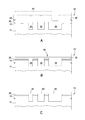
- 基板を研磨する方法であって、
回転可能なプラテンを有する研磨装置内で、複数のゾーンを有する基板を研磨してバルク材料層を除去すること
を含み、前記複数のゾーンのうちのそれぞれのゾーンの研磨速度が、独立に変更可能な研磨パラメータによって独立に制御可能であり、
前記方法がさらに、
バルクターゲット指標値を記憶すること、
研磨中に、前記複数のゾーンのうちのそれぞれのゾーンからの値の第1のシーケンスを、インシトゥモニタリングシステムを用いて測定すること、
前記複数のゾーンのうちのそれぞれのゾーンについて、前記値の第1のシーケンスに第1の線形関数を当てはめること、
前記複数のゾーンのうちの基準ゾーンについて、前記基準ゾーンが前記バルクターゲット指標値に到達する予測バルク終点時刻を、前記基準ゾーンの前記第1の線形関数に基づいて決定すること、ならびに
前記複数のゾーンのうちの少なくとも1つの調整可能ゾーンについて、前記調整可能ゾーンに対する前記研磨パラメータの第1の調整を計算して、前記調整可能ゾーンの研磨速度を調整すること
を含み、前記調整可能ゾーンの研磨速度の前記調整が、このような調整がなされない場合よりも、前記調整可能ゾーンが、前記予測バルク終点時刻において、前記バルクターゲット指標値により近くなるように実施され、前記計算が、以前の基板に対して計算された誤差値に基づいて前記第1の調整を計算することを含み、
前記方法がさらに、
前記研磨パラメータを調整した後に、それぞれのゾーンについて、研磨中に、前記研磨パラメータの前記第1の調整の後に得られた値の第2のシーケンスを測定すること、
それぞれの基板の前記少なくとも1つの調整可能ゾーンについて、前記値の第2のシーケンスに第2の線形関数を当てはめること、
後続の基板の前記少なくとも1つの調整可能ゾーンに対する誤差値を、前記第2の線形関数および所望の傾きに基づいて計算すること、
前記基準ゾーンの前記第1の線形関数または前記第2の線形関数がクリアリングターゲット指標値に到達する、残留材料除去の予測クリアリング終点時刻を決定すること、ならびに
少なくとも1つの調整可能ゾーンについて、前記調整可能ゾーンに対する前記研磨パラメータの第2の調整を計算して、前記調整可能ゾーンの研磨速度を調整すること
を含み、前記調整可能ゾーンの研磨速度の前記調整が、このような調整がなされない場合よりも、前記調整可能ゾーンが、前記予測クリアリング終点時刻において、前記クリアリングターゲット指標値により近くなるように実施され、前記計算が、以前の基板に対して計算された誤差値に基づいて前記調整を計算することを含み、
前記方法がさらに、
前記複数のゾーンの研磨を継続して、前記予測バルク終点時刻が過ぎるまで前記バルク材料層を除去すること、ならびに
前記調整可能ゾーンが、前記予測クリアリング終点時刻において、前記クリアリングターゲット指標値により近くなるように、前記第2の調整がなされた研磨パラメータを使用して前記複数のゾーンを研磨して、前記残留材料の層を除去すること
を含む方法。 - 前記基板が所定の時間、研磨され、前記バルクターゲット指標値が、前記所定の時間におけるプラテン回転数である、請求項1に記載の方法。
- 前記独立に変更可能な研磨パラメータが、前記研磨装置のキャリアヘッドによって前記基板の前記複数のゾーンのうち特定のゾーンの上に加えられる圧力である、請求項1に記載の方法。
- 前の基板に対して計算された前記誤差値が、前の1つまたは複数の基板の前記ゾーンの実際の研磨速度の、それらの前の基板の前記ゾーンに対する所望の研磨速度からの変動に基づく、請求項1に記載の方法。
- 前の基板に対して計算された前記誤差値が、前記調整可能ゾーン上の圧力に対する修正を調整するスケーリング因子として使用される、請求項4に記載の方法。
- 前記インシトゥモニタリングシステムが分光写真モニタリングシステムである、請求項1に記載の方法。
- 前記予測バルク終点時刻が、モータトルクモニタリングシステム、渦電流モニタリングシステム、摩擦モニタリングシステムまたは単色光学システムのうちの少なくとも1つのシステムを使用して検出される、請求項1に記載の方法。
- 前記予測バルク終点時刻が、多数のゾーンの予測終点時刻の結合として予め決定されまたは計算される、請求項1に記載の方法。
- 前記予測バルク終点時刻が、以前に研磨された基板のバルク終点時刻に基づいて決定される、請求項1に記載の方法。
- 前の基板に対して計算された前記誤差値が、前の1つまたは複数の基板の前記ゾーンの実際の研磨速度の、それらの前の基板の前記ゾーンに対する所望の研磨速度からの変動に基づく、請求項1に記載の方法。
- 前の基板に対して計算された前記誤差値が、前記調整可能ゾーン上の圧力に対する修正を調整するスケーリング因子として使用される、請求項10に記載の方法。
- 基板を研磨する方法であって、
回転可能なプラテンを有する研磨装置内で、複数のゾーンを有する基板を研磨してバルク材料層を除去すること
を含み、前記複数のゾーンのうちのそれぞれのゾーンの研磨速度が、独立に変更可能な研磨パラメータによって独立に制御可能であり、
前記方法がさらに、
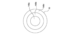
前記複数のゾーンのうちのそれぞれのゾーンについて、現在のプラテン回転に対する測定スペクトルを得ること、
前記複数のゾーンのうちのそれぞれのゾーンについて、前記測定スペクトルに対するベストマッチである基準スペクトルを決定すること、
ベストフィットであるそれぞれの基準スペクトルの指標値を決定することによって指標値のシーケンスを生成すること、
前記複数のゾーンのうちのそれぞれのゾーンについて、前記指標値のシーケンスに第1の線形関数を当てはめること、
前記複数のゾーンのうちの基準ゾーンの前記第1の線形関数がバルクターゲット指標値に到達する予測バルク終点時刻を決定すること、
前の任意の基板からの誤差値を使用することを含む、前記複数のゾーンのうちのそれぞれのゾーンの研磨パラメータを、前記複数のゾーンが前記予測バルク終点時刻にほぼ同じ指標値を有するように調整すること、
研磨を継続し、スペクトルを測定し、誤差値および指標値の第2のシーケンスを決定し、前記指標値の第2のシーケンスに第2の線形関数を当てはめること、
前記基準ゾーンの前記第1の線形関数または前記第2の線形関数がクリアリングターゲット指標値に到達する予測クリアリング終点時刻を決定すること、
前記複数のゾーンの研磨を継続して、前記予測バルク終点時刻が過ぎるまで前記バルク材料層を除去すること、ならびに
前の任意の基板からの誤差値を使用することを含む、前記予測バルク終点時刻が過ぎた後に、研磨パラメータを調整して、前記複数のゾーンを研磨し、それによって残留材料層を除去すること
を含む方法。 - 前記予測バルク終点時刻が過ぎた後に残留材料層を除去することが、
前記複数のゾーンのうちのそれぞれのゾーンについて、前記測定スペクトルに対するベストマッチである基準スペクトルを決定すること、
ベストフィットであるそれぞれの基準スペクトルの指標値を決定することによって指標値のシーケンスを生成すること、
前記複数のゾーンのうちのそれぞれのゾーンについて、前記指標値のシーケンスに第1の線形関数を当てはめること、
前記基準ゾーンの前記第1の線形関数がクリアリングターゲット指標値に到達する予測クリアリング終点時刻を調整すること、および
前記基準ゾーンが調整された前記予測クリアリング終点時刻に到達するまで研磨すること
をさらに含む、請求項12に記載の方法。 - 前記予測バルク終点時刻が過ぎた後に残留材料層を除去することが、
指標値の新しいシーケンスを決定し、前記指標値の新しいシーケンスに第2の線形関数を当てはめること、および
後続の基板の研磨にフィードバックする誤差値を決定すること
をさらに含む、請求項13に記載の方法。 - 1つまたは複数の新たな基板を研磨パッド上に装填すること、
調整された前記研磨パラメータに基づいて前記1つまたは複数の新たな基板を研磨すること
をさらに含む、請求項14に記載の方法。 - 前記1つまたは複数の新たな基板の前記複数のゾーンのうちのそれぞれのゾーンについて、現在のプラテン回転に対する測定スペクトルを得ること、
前記1つまたは複数の新たな基板の前記複数のゾーンのうちのそれぞれのゾーンについて、前記測定スペクトルに対するベストマッチである基準スペクトルを決定すること、および
前記1つまたは複数の新たな基板について、ベストフィットであるそれぞれの基準スペクトルの指標値を決定することによって指標値のシーケンスを生成すること、
をさらに含む、請求項15に記載の方法。 - 前記独立に変更可能な研磨パラメータが、前記研磨装置のキャリアヘッドの圧力である、請求項12に記載の方法。
- 前記基板が所定の時間、研磨され、前記バルクターゲット指標値が、前記所定の時間におけるプラテン回転数である、請求項12に記載の方法。
- 前記測定スペクトルが、インシトゥ分光写真モニタリングシステムを使用して得られる、請求項12に記載の方法。
- 前記予測バルク終点時刻が、モータトルクモニタリングシステム、渦電流モニタリングシステム、摩擦モニタリングシステムまたは単色光学システムのうちの少なくとも1つのシステムを使用して検出される、請求項12に記載の方法。
Applications Claiming Priority (3)
| Application Number | Priority Date | Filing Date | Title |
|---|---|---|---|
| US201361787221P | 2013-03-15 | 2013-03-15 | |
| US61/787,221 | 2013-03-15 | ||
| PCT/US2014/017277 WO2014149330A1 (en) | 2013-03-15 | 2014-02-20 | Dynamic residue clearing control with in-situ profile control (ispc) |
Publications (3)
| Publication Number | Publication Date |
|---|---|
| JP2016510953A JP2016510953A (ja) | 2016-04-11 |
| JP2016510953A5 JP2016510953A5 (ja) | 2016-11-04 |
| JP6060308B2 true JP6060308B2 (ja) | 2017-01-11 |
Family
ID=51529181
Family Applications (1)
| Application Number | Title | Priority Date | Filing Date |
|---|---|---|---|
| JP2016500309A Active JP6060308B2 (ja) | 2013-03-15 | 2014-02-20 | インシトゥプロファイル制御(ispc)を用いた残留物クリアリングの動的制御 |
Country Status (5)
| Country | Link |
|---|---|
| US (1) | US9242337B2 (ja) |
| JP (1) | JP6060308B2 (ja) |
| KR (1) | KR101699197B1 (ja) |
| TW (1) | TWI564946B (ja) |
| WO (1) | WO2014149330A1 (ja) |
Families Citing this family (11)
| Publication number | Priority date | Publication date | Assignee | Title |
|---|---|---|---|---|
| US9248544B2 (en) * | 2012-07-18 | 2016-02-02 | Applied Materials, Inc. | Endpoint detection during polishing using integrated differential intensity |
| JP6447472B2 (ja) | 2015-11-26 | 2019-01-09 | 株式会社Sumco | ウェーハ研磨方法 |
| JP6406238B2 (ja) * | 2015-12-18 | 2018-10-17 | 株式会社Sumco | ウェーハ研磨方法および研磨装置 |
| WO2018071302A1 (en) * | 2016-10-10 | 2018-04-19 | Applied Materials, Inc. | Real time profile control for chemical mechanical polishing |
| WO2018075260A1 (en) | 2016-10-21 | 2018-04-26 | Applied Materials, Inc. | Core configuration for in-situ electromagnetic induction monitoring system |
| KR102525737B1 (ko) * | 2016-11-16 | 2023-04-26 | 주식회사 케이씨텍 | 화학 기계적 연마장치 및 그 제어방법 |
| US20200210547A1 (en) * | 2018-12-26 | 2020-07-02 | Applied Materials, Inc. | Preston Matrix Generator |
| EP3917721A4 (en) * | 2019-01-31 | 2022-10-26 | The Hillman Group, Inc. | AUTOMATIC KNIFE SHARPENING MACHINE WITH EDGE DETECTION |
| JP7446714B2 (ja) * | 2019-02-01 | 2024-03-11 | 株式会社荏原製作所 | 基板処理装置、および基板処理方法 |
| TWI809389B (zh) * | 2020-06-08 | 2023-07-21 | 美商應用材料股份有限公司 | 用於在拋光相鄰導電層的堆疊期間的輪廓控制的系統、方法及電腦程式產品 |
| US20220283554A1 (en) * | 2021-03-05 | 2022-09-08 | Applied Materials, Inc. | Control of processing parameters for substrate polishing with substrate precession |
Family Cites Families (22)
| Publication number | Priority date | Publication date | Assignee | Title |
|---|---|---|---|---|
| EP1322940A4 (en) | 2000-07-31 | 2006-03-15 | Asml Us Inc | METHOD AND IN SITU DEVICE FOR DETECTING THE TURN POINT FOR CHEMICAL MECHANICAL POLISHING |
| US6929531B2 (en) * | 2002-09-19 | 2005-08-16 | Lam Research Corporation | System and method for metal residue detection and mapping within a multi-step sequence |
| US7063597B2 (en) | 2002-10-25 | 2006-06-20 | Applied Materials | Polishing processes for shallow trench isolation substrates |
| JP4994227B2 (ja) * | 2004-06-21 | 2012-08-08 | 株式会社荏原製作所 | 研磨装置および研磨方法 |
| US7084064B2 (en) | 2004-09-14 | 2006-08-01 | Applied Materials, Inc. | Full sequence metal and barrier layer electrochemical mechanical processing |
| JP5534672B2 (ja) * | 2005-08-22 | 2014-07-02 | アプライド マテリアルズ インコーポレイテッド | 化学機械的研磨のスペクトルに基づく監視のための装置および方法 |
| US8392012B2 (en) | 2008-10-27 | 2013-03-05 | Applied Materials, Inc. | Multiple libraries for spectrographic monitoring of zones of a substrate during processing |
| US20070108066A1 (en) * | 2005-10-28 | 2007-05-17 | Applied Materials, Inc. | Voltage mode current control |
| US20070158201A1 (en) | 2006-01-06 | 2007-07-12 | Applied Materials, Inc. | Electrochemical processing with dynamic process control |
| TWI286094B (en) * | 2006-05-18 | 2007-09-01 | United Microelectronics Corp | Method for in-line controlling hybrid chemical mechanical polishing process |
| US8246417B2 (en) * | 2006-09-12 | 2012-08-21 | Ebara Corporation | Polishing apparatus and polishing method |
| KR101834944B1 (ko) * | 2008-09-04 | 2018-03-06 | 어플라이드 머티어리얼스, 인코포레이티드 | 프로세싱 동안 기판의 분광 모니터링의 이용에 의한 연마 속도들의 조정 |
| US8039397B2 (en) | 2008-11-26 | 2011-10-18 | Applied Materials, Inc. | Using optical metrology for within wafer feed forward process control |
| US9579767B2 (en) | 2010-04-28 | 2017-02-28 | Applied Materials, Inc. | Automatic generation of reference spectra for optical monitoring of substrates |
| US8190285B2 (en) | 2010-05-17 | 2012-05-29 | Applied Materials, Inc. | Feedback for polishing rate correction in chemical mechanical polishing |
| US8616935B2 (en) * | 2010-06-02 | 2013-12-31 | Applied Materials, Inc. | Control of overpolishing of multiple substrates on the same platen in chemical mechanical polishing |
| US20120034844A1 (en) | 2010-08-05 | 2012-02-09 | Applied Materials, Inc. | Spectrographic monitoring using index tracking after detection of layer clearing |
| TW201223702A (en) * | 2010-08-06 | 2012-06-16 | Applied Materials Inc | Techniques for matching measured spectra to reference spectra for in-situ optical monitoring |
| TW201223703A (en) * | 2010-09-01 | 2012-06-16 | Applied Materials Inc | Feedback control of polishing using optical detection of clearance |
| US20120276817A1 (en) * | 2011-04-27 | 2012-11-01 | Iravani Hassan G | Eddy current monitoring of metal residue or metal pillars |
| JP6050571B2 (ja) | 2011-08-09 | 2016-12-21 | 株式会社荏原製作所 | 研磨監視方法および研磨装置 |
| US9095952B2 (en) * | 2013-01-23 | 2015-08-04 | Applied Materials, Inc. | Reflectivity measurements during polishing using a camera |
-
2014
- 2014-02-20 WO PCT/US2014/017277 patent/WO2014149330A1/en active Application Filing
- 2014-02-20 US US14/185,185 patent/US9242337B2/en active Active
- 2014-02-20 KR KR1020157029826A patent/KR101699197B1/ko active IP Right Grant
- 2014-02-20 JP JP2016500309A patent/JP6060308B2/ja active Active
- 2014-03-07 TW TW103107921A patent/TWI564946B/zh active
Also Published As
| Publication number | Publication date |
|---|---|
| WO2014149330A1 (en) | 2014-09-25 |
| JP2016510953A (ja) | 2016-04-11 |
| TW201503244A (zh) | 2015-01-16 |
| TWI564946B (zh) | 2017-01-01 |
| US9242337B2 (en) | 2016-01-26 |
| KR101699197B1 (ko) | 2017-01-23 |
| US20140273749A1 (en) | 2014-09-18 |
| KR20150132524A (ko) | 2015-11-25 |
Similar Documents
| Publication | Publication Date | Title |
|---|---|---|
| JP6060308B2 (ja) | インシトゥプロファイル制御(ispc)を用いた残留物クリアリングの動的制御 | |
| US8755927B2 (en) | Feedback for polishing rate correction in chemical mechanical polishing | |
| US10589397B2 (en) | Endpoint control of multiple substrate zones of varying thickness in chemical mechanical polishing | |
| US8874250B2 (en) | Spectrographic monitoring of a substrate during processing using index values | |
| US8751033B2 (en) | Adaptive tracking spectrum features for endpoint detection | |
| US9372116B2 (en) | Automatic initiation of reference spectra library generation for optical monitoring | |
| US20120034845A1 (en) | Techniques for matching measured spectra to reference spectra for in-situ optical monitoring | |
| US20170100814A1 (en) | Polishing apparatus having optical monitoring of substrates for uniformity control and separate endpoint system | |
| US20110300775A1 (en) | Control of Overpolishing of Multiple Substrates on the Same Platen in Chemical Mechanical Polishing | |
| US20120034844A1 (en) | Spectrographic monitoring using index tracking after detection of layer clearing | |
| US20110282477A1 (en) | Endpoint control of multiple substrates with multiple zones on the same platen in chemical mechanical polishing | |
| US20120100781A1 (en) | Multiple matching reference spectra for in-situ optical monitoring | |
| TWI496661B (zh) | 用於光學監測之參考光譜的自動產生 | |
| JP2013532912A (ja) | 基板上の複数のゾーンを監視するための基準ライブラリの選択 |
Legal Events
| Date | Code | Title | Description |
|---|---|---|---|
| A521 | Request for written amendment filed |
Free format text: JAPANESE INTERMEDIATE CODE: A523 Effective date: 20160909 |
|
| A621 | Written request for application examination |
Free format text: JAPANESE INTERMEDIATE CODE: A621 Effective date: 20160909 |
|
| A871 | Explanation of circumstances concerning accelerated examination |
Free format text: JAPANESE INTERMEDIATE CODE: A871 Effective date: 20160909 |
|
| A975 | Report on accelerated examination |
Free format text: JAPANESE INTERMEDIATE CODE: A971005 Effective date: 20161028 |
|
| TRDD | Decision of grant or rejection written | ||
| A01 | Written decision to grant a patent or to grant a registration (utility model) |
Free format text: JAPANESE INTERMEDIATE CODE: A01 Effective date: 20161115 |
|
| A61 | First payment of annual fees (during grant procedure) |
Free format text: JAPANESE INTERMEDIATE CODE: A61 Effective date: 20161212 |
|
| R150 | Certificate of patent or registration of utility model |
Ref document number: 6060308 Country of ref document: JP Free format text: JAPANESE INTERMEDIATE CODE: R150 |
|
| R250 | Receipt of annual fees |
Free format text: JAPANESE INTERMEDIATE CODE: R250 |
|
| R250 | Receipt of annual fees |
Free format text: JAPANESE INTERMEDIATE CODE: R250 |
|
| R250 | Receipt of annual fees |
Free format text: JAPANESE INTERMEDIATE CODE: R250 |
|
| R250 | Receipt of annual fees |
Free format text: JAPANESE INTERMEDIATE CODE: R250 |
|
| R250 | Receipt of annual fees |
Free format text: JAPANESE INTERMEDIATE CODE: R250 |