JP6056403B2 - Deposition equipment - Google Patents
Deposition equipment Download PDFInfo
- Publication number
- JP6056403B2 JP6056403B2 JP2012251595A JP2012251595A JP6056403B2 JP 6056403 B2 JP6056403 B2 JP 6056403B2 JP 2012251595 A JP2012251595 A JP 2012251595A JP 2012251595 A JP2012251595 A JP 2012251595A JP 6056403 B2 JP6056403 B2 JP 6056403B2
- Authority
- JP
- Japan
- Prior art keywords
- mounting table
- clamp ring
- substrate
- surrounding member
- processing
- Prior art date
- Legal status (The legal status is an assumption and is not a legal conclusion. Google has not performed a legal analysis and makes no representation as to the accuracy of the status listed.)
- Active
Links
- 230000008021 deposition Effects 0.000 title description 6
- 238000012545 processing Methods 0.000 claims description 92
- 239000007789 gas Substances 0.000 claims description 83
- 239000012495 reaction gas Substances 0.000 claims description 41
- 239000000758 substrate Substances 0.000 claims description 39
- 238000010926 purge Methods 0.000 claims description 37
- 230000002093 peripheral effect Effects 0.000 claims description 35
- 238000000034 method Methods 0.000 claims description 28
- 238000012546 transfer Methods 0.000 claims description 22
- 229910052751 metal Inorganic materials 0.000 claims description 17
- 239000002184 metal Substances 0.000 claims description 16
- 230000008569 process Effects 0.000 claims description 15
- PXHVJJICTQNCMI-UHFFFAOYSA-N Nickel Chemical compound [Ni] PXHVJJICTQNCMI-UHFFFAOYSA-N 0.000 claims description 12
- 238000010438 heat treatment Methods 0.000 claims description 12
- 230000001590 oxidative effect Effects 0.000 claims description 10
- 229910052759 nickel Inorganic materials 0.000 claims description 5
- 239000002245 particle Substances 0.000 claims description 5
- 229910052707 ruthenium Inorganic materials 0.000 claims description 5
- KJTLSVCANCCWHF-UHFFFAOYSA-N Ruthenium Chemical compound [Ru] KJTLSVCANCCWHF-UHFFFAOYSA-N 0.000 claims description 3
- 239000010408 film Substances 0.000 description 80
- MYMOFIZGZYHOMD-UHFFFAOYSA-N Dioxygen Chemical compound O=O MYMOFIZGZYHOMD-UHFFFAOYSA-N 0.000 description 19
- 229910001882 dioxygen Inorganic materials 0.000 description 19
- 238000006243 chemical reaction Methods 0.000 description 11
- 230000000694 effects Effects 0.000 description 10
- 230000015572 biosynthetic process Effects 0.000 description 7
- 238000000231 atomic layer deposition Methods 0.000 description 6
- 238000000151 deposition Methods 0.000 description 6
- 230000003028 elevating effect Effects 0.000 description 6
- IJGRMHOSHXDMSA-UHFFFAOYSA-N Atomic nitrogen Chemical compound N#N IJGRMHOSHXDMSA-UHFFFAOYSA-N 0.000 description 5
- 229910052782 aluminium Inorganic materials 0.000 description 5
- 229910001873 dinitrogen Inorganic materials 0.000 description 5
- 230000007246 mechanism Effects 0.000 description 5
- 238000002161 passivation Methods 0.000 description 5
- 230000009471 action Effects 0.000 description 4
- XAGFODPZIPBFFR-UHFFFAOYSA-N aluminium Chemical compound [Al] XAGFODPZIPBFFR-UHFFFAOYSA-N 0.000 description 4
- 238000005229 chemical vapour deposition Methods 0.000 description 4
- 230000000737 periodic effect Effects 0.000 description 4
- 230000035699 permeability Effects 0.000 description 4
- 238000003860 storage Methods 0.000 description 4
- QVGXLLKOCUKJST-UHFFFAOYSA-N atomic oxygen Chemical compound [O] QVGXLLKOCUKJST-UHFFFAOYSA-N 0.000 description 3
- 230000000052 comparative effect Effects 0.000 description 3
- 238000010586 diagram Methods 0.000 description 3
- 239000007800 oxidant agent Substances 0.000 description 3
- 239000001301 oxygen Substances 0.000 description 3
- 229910052760 oxygen Inorganic materials 0.000 description 3
- 239000010453 quartz Substances 0.000 description 3
- VYPSYNLAJGMNEJ-UHFFFAOYSA-N silicon dioxide Inorganic materials O=[Si]=O VYPSYNLAJGMNEJ-UHFFFAOYSA-N 0.000 description 3
- UFHFLCQGNIYNRP-UHFFFAOYSA-N Hydrogen Chemical compound [H][H] UFHFLCQGNIYNRP-UHFFFAOYSA-N 0.000 description 2
- 239000007795 chemical reaction product Substances 0.000 description 2
- 238000011109 contamination Methods 0.000 description 2
- 150000002736 metal compounds Chemical class 0.000 description 2
- 239000002052 molecular layer Substances 0.000 description 2
- 238000005192 partition Methods 0.000 description 2
- 239000002994 raw material Substances 0.000 description 2
- 238000006722 reduction reaction Methods 0.000 description 2
- 239000004065 semiconductor Substances 0.000 description 2
- 238000011144 upstream manufacturing Methods 0.000 description 2
- -1 CH 3 OH Chemical class 0.000 description 1
- BDAGIHXWWSANSR-UHFFFAOYSA-N Formic acid Chemical compound OC=O BDAGIHXWWSANSR-UHFFFAOYSA-N 0.000 description 1
- 241001417935 Platycephalidae Species 0.000 description 1
- 150000001298 alcohols Chemical class 0.000 description 1
- PNEYBMLMFCGWSK-UHFFFAOYSA-N aluminium oxide Inorganic materials [O-2].[O-2].[O-2].[Al+3].[Al+3] PNEYBMLMFCGWSK-UHFFFAOYSA-N 0.000 description 1
- 239000006227 byproduct Substances 0.000 description 1
- 238000003763 carbonization Methods 0.000 description 1
- 239000000919 ceramic Substances 0.000 description 1
- 229910052804 chromium Inorganic materials 0.000 description 1
- 238000004891 communication Methods 0.000 description 1
- 238000007796 conventional method Methods 0.000 description 1
- 229910052802 copper Inorganic materials 0.000 description 1
- PMHQVHHXPFUNSP-UHFFFAOYSA-M copper(1+);methylsulfanylmethane;bromide Chemical compound Br[Cu].CSC PMHQVHHXPFUNSP-UHFFFAOYSA-M 0.000 description 1
- 238000005520 cutting process Methods 0.000 description 1
- 238000002474 experimental method Methods 0.000 description 1
- 235000019253 formic acid Nutrition 0.000 description 1
- 229910052732 germanium Inorganic materials 0.000 description 1
- 230000009545 invasion Effects 0.000 description 1
- 229910052742 iron Inorganic materials 0.000 description 1
- 238000005304 joining Methods 0.000 description 1
- 229910052748 manganese Inorganic materials 0.000 description 1
- 239000000463 material Substances 0.000 description 1
- 239000012528 membrane Substances 0.000 description 1
- 150000002739 metals Chemical class 0.000 description 1
- 238000012986 modification Methods 0.000 description 1
- 230000004048 modification Effects 0.000 description 1
- 229910052750 molybdenum Inorganic materials 0.000 description 1
- 125000000896 monocarboxylic acid group Chemical group 0.000 description 1
- 238000005121 nitriding Methods 0.000 description 1
- 230000003287 optical effect Effects 0.000 description 1
- 150000007524 organic acids Chemical class 0.000 description 1
- 235000005985 organic acids Nutrition 0.000 description 1
- 238000007254 oxidation reaction Methods 0.000 description 1
- 229910052763 palladium Inorganic materials 0.000 description 1
- 230000000149 penetrating effect Effects 0.000 description 1
- 230000035515 penetration Effects 0.000 description 1
- 238000005268 plasma chemical vapour deposition Methods 0.000 description 1
- 229910052697 platinum Inorganic materials 0.000 description 1
- 238000003825 pressing Methods 0.000 description 1
- 230000009467 reduction Effects 0.000 description 1
- 229910052702 rhenium Inorganic materials 0.000 description 1
- 229910052703 rhodium Inorganic materials 0.000 description 1
- WOCIAKWEIIZHES-UHFFFAOYSA-N ruthenium(iv) oxide Chemical compound O=[Ru]=O WOCIAKWEIIZHES-UHFFFAOYSA-N 0.000 description 1
- 229910052709 silver Inorganic materials 0.000 description 1
- 230000002195 synergetic effect Effects 0.000 description 1
- 229910052715 tantalum Inorganic materials 0.000 description 1
- 238000002230 thermal chemical vapour deposition Methods 0.000 description 1
- 239000010409 thin film Substances 0.000 description 1
- 229910052719 titanium Inorganic materials 0.000 description 1
- 229910052721 tungsten Inorganic materials 0.000 description 1
- 238000009834 vaporization Methods 0.000 description 1
- 230000008016 vaporization Effects 0.000 description 1
- 229910052725 zinc Inorganic materials 0.000 description 1
- 229910052726 zirconium Inorganic materials 0.000 description 1
Images


Classifications
-
- C—CHEMISTRY; METALLURGY
- C23—COATING METALLIC MATERIAL; COATING MATERIAL WITH METALLIC MATERIAL; CHEMICAL SURFACE TREATMENT; DIFFUSION TREATMENT OF METALLIC MATERIAL; COATING BY VACUUM EVAPORATION, BY SPUTTERING, BY ION IMPLANTATION OR BY CHEMICAL VAPOUR DEPOSITION, IN GENERAL; INHIBITING CORROSION OF METALLIC MATERIAL OR INCRUSTATION IN GENERAL
- C23C—COATING METALLIC MATERIAL; COATING MATERIAL WITH METALLIC MATERIAL; SURFACE TREATMENT OF METALLIC MATERIAL BY DIFFUSION INTO THE SURFACE, BY CHEMICAL CONVERSION OR SUBSTITUTION; COATING BY VACUUM EVAPORATION, BY SPUTTERING, BY ION IMPLANTATION OR BY CHEMICAL VAPOUR DEPOSITION, IN GENERAL
- C23C16/00—Chemical coating by decomposition of gaseous compounds, without leaving reaction products of surface material in the coating, i.e. chemical vapour deposition [CVD] processes
- C23C16/44—Chemical coating by decomposition of gaseous compounds, without leaving reaction products of surface material in the coating, i.e. chemical vapour deposition [CVD] processes characterised by the method of coating
- C23C16/455—Chemical coating by decomposition of gaseous compounds, without leaving reaction products of surface material in the coating, i.e. chemical vapour deposition [CVD] processes characterised by the method of coating characterised by the method used for introducing gases into reaction chamber or for modifying gas flows in reaction chamber
- C23C16/45523—Pulsed gas flow or change of composition over time
- C23C16/45525—Atomic layer deposition [ALD]
- C23C16/45544—Atomic layer deposition [ALD] characterized by the apparatus
-
- C—CHEMISTRY; METALLURGY
- C23—COATING METALLIC MATERIAL; COATING MATERIAL WITH METALLIC MATERIAL; CHEMICAL SURFACE TREATMENT; DIFFUSION TREATMENT OF METALLIC MATERIAL; COATING BY VACUUM EVAPORATION, BY SPUTTERING, BY ION IMPLANTATION OR BY CHEMICAL VAPOUR DEPOSITION, IN GENERAL; INHIBITING CORROSION OF METALLIC MATERIAL OR INCRUSTATION IN GENERAL
- C23C—COATING METALLIC MATERIAL; COATING MATERIAL WITH METALLIC MATERIAL; SURFACE TREATMENT OF METALLIC MATERIAL BY DIFFUSION INTO THE SURFACE, BY CHEMICAL CONVERSION OR SUBSTITUTION; COATING BY VACUUM EVAPORATION, BY SPUTTERING, BY ION IMPLANTATION OR BY CHEMICAL VAPOUR DEPOSITION, IN GENERAL
- C23C16/00—Chemical coating by decomposition of gaseous compounds, without leaving reaction products of surface material in the coating, i.e. chemical vapour deposition [CVD] processes
- C23C16/44—Chemical coating by decomposition of gaseous compounds, without leaving reaction products of surface material in the coating, i.e. chemical vapour deposition [CVD] processes characterised by the method of coating
- C23C16/4412—Details relating to the exhausts, e.g. pumps, filters, scrubbers, particle traps
-
- C—CHEMISTRY; METALLURGY
- C23—COATING METALLIC MATERIAL; COATING MATERIAL WITH METALLIC MATERIAL; CHEMICAL SURFACE TREATMENT; DIFFUSION TREATMENT OF METALLIC MATERIAL; COATING BY VACUUM EVAPORATION, BY SPUTTERING, BY ION IMPLANTATION OR BY CHEMICAL VAPOUR DEPOSITION, IN GENERAL; INHIBITING CORROSION OF METALLIC MATERIAL OR INCRUSTATION IN GENERAL
- C23C—COATING METALLIC MATERIAL; COATING MATERIAL WITH METALLIC MATERIAL; SURFACE TREATMENT OF METALLIC MATERIAL BY DIFFUSION INTO THE SURFACE, BY CHEMICAL CONVERSION OR SUBSTITUTION; COATING BY VACUUM EVAPORATION, BY SPUTTERING, BY ION IMPLANTATION OR BY CHEMICAL VAPOUR DEPOSITION, IN GENERAL
- C23C16/00—Chemical coating by decomposition of gaseous compounds, without leaving reaction products of surface material in the coating, i.e. chemical vapour deposition [CVD] processes
- C23C16/44—Chemical coating by decomposition of gaseous compounds, without leaving reaction products of surface material in the coating, i.e. chemical vapour deposition [CVD] processes characterised by the method of coating
- C23C16/455—Chemical coating by decomposition of gaseous compounds, without leaving reaction products of surface material in the coating, i.e. chemical vapour deposition [CVD] processes characterised by the method of coating characterised by the method used for introducing gases into reaction chamber or for modifying gas flows in reaction chamber
- C23C16/45563—Gas nozzles
- C23C16/45565—Shower nozzles
-
- C—CHEMISTRY; METALLURGY
- C23—COATING METALLIC MATERIAL; COATING MATERIAL WITH METALLIC MATERIAL; CHEMICAL SURFACE TREATMENT; DIFFUSION TREATMENT OF METALLIC MATERIAL; COATING BY VACUUM EVAPORATION, BY SPUTTERING, BY ION IMPLANTATION OR BY CHEMICAL VAPOUR DEPOSITION, IN GENERAL; INHIBITING CORROSION OF METALLIC MATERIAL OR INCRUSTATION IN GENERAL
- C23C—COATING METALLIC MATERIAL; COATING MATERIAL WITH METALLIC MATERIAL; SURFACE TREATMENT OF METALLIC MATERIAL BY DIFFUSION INTO THE SURFACE, BY CHEMICAL CONVERSION OR SUBSTITUTION; COATING BY VACUUM EVAPORATION, BY SPUTTERING, BY ION IMPLANTATION OR BY CHEMICAL VAPOUR DEPOSITION, IN GENERAL
- C23C16/00—Chemical coating by decomposition of gaseous compounds, without leaving reaction products of surface material in the coating, i.e. chemical vapour deposition [CVD] processes
- C23C16/44—Chemical coating by decomposition of gaseous compounds, without leaving reaction products of surface material in the coating, i.e. chemical vapour deposition [CVD] processes characterised by the method of coating
- C23C16/455—Chemical coating by decomposition of gaseous compounds, without leaving reaction products of surface material in the coating, i.e. chemical vapour deposition [CVD] processes characterised by the method of coating characterised by the method used for introducing gases into reaction chamber or for modifying gas flows in reaction chamber
- C23C16/45563—Gas nozzles
- C23C16/45574—Nozzles for more than one gas
-
- C—CHEMISTRY; METALLURGY
- C23—COATING METALLIC MATERIAL; COATING MATERIAL WITH METALLIC MATERIAL; CHEMICAL SURFACE TREATMENT; DIFFUSION TREATMENT OF METALLIC MATERIAL; COATING BY VACUUM EVAPORATION, BY SPUTTERING, BY ION IMPLANTATION OR BY CHEMICAL VAPOUR DEPOSITION, IN GENERAL; INHIBITING CORROSION OF METALLIC MATERIAL OR INCRUSTATION IN GENERAL
- C23C—COATING METALLIC MATERIAL; COATING MATERIAL WITH METALLIC MATERIAL; SURFACE TREATMENT OF METALLIC MATERIAL BY DIFFUSION INTO THE SURFACE, BY CHEMICAL CONVERSION OR SUBSTITUTION; COATING BY VACUUM EVAPORATION, BY SPUTTERING, BY ION IMPLANTATION OR BY CHEMICAL VAPOUR DEPOSITION, IN GENERAL
- C23C16/00—Chemical coating by decomposition of gaseous compounds, without leaving reaction products of surface material in the coating, i.e. chemical vapour deposition [CVD] processes
- C23C16/44—Chemical coating by decomposition of gaseous compounds, without leaving reaction products of surface material in the coating, i.e. chemical vapour deposition [CVD] processes characterised by the method of coating
- C23C16/458—Chemical coating by decomposition of gaseous compounds, without leaving reaction products of surface material in the coating, i.e. chemical vapour deposition [CVD] processes characterised by the method of coating characterised by the method used for supporting substrates in the reaction chamber
- C23C16/4582—Rigid and flat substrates, e.g. plates or discs
- C23C16/4583—Rigid and flat substrates, e.g. plates or discs the substrate being supported substantially horizontally
- C23C16/4585—Devices at or outside the perimeter of the substrate support, e.g. clamping rings, shrouds
-
- H—ELECTRICITY
- H01—ELECTRIC ELEMENTS
- H01L—SEMICONDUCTOR DEVICES NOT COVERED BY CLASS H10
- H01L21/00—Processes or apparatus adapted for the manufacture or treatment of semiconductor or solid state devices or of parts thereof
- H01L21/02—Manufacture or treatment of semiconductor devices or of parts thereof
- H01L21/02104—Forming layers
- H01L21/02107—Forming insulating materials on a substrate
- H01L21/02109—Forming insulating materials on a substrate characterised by the type of layer, e.g. type of material, porous/non-porous, pre-cursors, mixtures or laminates
- H01L21/02112—Forming insulating materials on a substrate characterised by the type of layer, e.g. type of material, porous/non-porous, pre-cursors, mixtures or laminates characterised by the material of the layer
- H01L21/02172—Forming insulating materials on a substrate characterised by the type of layer, e.g. type of material, porous/non-porous, pre-cursors, mixtures or laminates characterised by the material of the layer the material containing at least one metal element, e.g. metal oxides, metal nitrides, metal oxynitrides or metal carbides
- H01L21/02175—Forming insulating materials on a substrate characterised by the type of layer, e.g. type of material, porous/non-porous, pre-cursors, mixtures or laminates characterised by the material of the layer the material containing at least one metal element, e.g. metal oxides, metal nitrides, metal oxynitrides or metal carbides characterised by the metal
-
- H—ELECTRICITY
- H01—ELECTRIC ELEMENTS
- H01L—SEMICONDUCTOR DEVICES NOT COVERED BY CLASS H10
- H01L21/00—Processes or apparatus adapted for the manufacture or treatment of semiconductor or solid state devices or of parts thereof
- H01L21/67—Apparatus specially adapted for handling semiconductor or electric solid state devices during manufacture or treatment thereof; Apparatus specially adapted for handling wafers during manufacture or treatment of semiconductor or electric solid state devices or components ; Apparatus not specifically provided for elsewhere
- H01L21/683—Apparatus specially adapted for handling semiconductor or electric solid state devices during manufacture or treatment thereof; Apparatus specially adapted for handling wafers during manufacture or treatment of semiconductor or electric solid state devices or components ; Apparatus not specifically provided for elsewhere for supporting or gripping
- H01L21/687—Apparatus specially adapted for handling semiconductor or electric solid state devices during manufacture or treatment thereof; Apparatus specially adapted for handling wafers during manufacture or treatment of semiconductor or electric solid state devices or components ; Apparatus not specifically provided for elsewhere for supporting or gripping using mechanical means, e.g. chucks, clamps or pinches
- H01L21/68714—Apparatus specially adapted for handling semiconductor or electric solid state devices during manufacture or treatment thereof; Apparatus specially adapted for handling wafers during manufacture or treatment of semiconductor or electric solid state devices or components ; Apparatus not specifically provided for elsewhere for supporting or gripping using mechanical means, e.g. chucks, clamps or pinches the wafers being placed on a susceptor, stage or support
- H01L21/68721—Apparatus specially adapted for handling semiconductor or electric solid state devices during manufacture or treatment thereof; Apparatus specially adapted for handling wafers during manufacture or treatment of semiconductor or electric solid state devices or components ; Apparatus not specifically provided for elsewhere for supporting or gripping using mechanical means, e.g. chucks, clamps or pinches the wafers being placed on a susceptor, stage or support characterised by edge clamping, e.g. clamping ring
Landscapes
- Chemical & Material Sciences (AREA)
- Engineering & Computer Science (AREA)
- General Chemical & Material Sciences (AREA)
- Chemical Kinetics & Catalysis (AREA)
- Materials Engineering (AREA)
- Mechanical Engineering (AREA)
- Metallurgy (AREA)
- Organic Chemistry (AREA)
- Physics & Mathematics (AREA)
- Condensed Matter Physics & Semiconductors (AREA)
- General Physics & Mathematics (AREA)
- Manufacturing & Machinery (AREA)
- Computer Hardware Design (AREA)
- Microelectronics & Electronic Packaging (AREA)
- Power Engineering (AREA)
- Chemical Vapour Deposition (AREA)
- Electrodes Of Semiconductors (AREA)
Description
本発明は、処理容器内の基板に対して反応ガスを供給して成膜処理を行う成膜装置に関する。 The present invention relates to a film forming apparatus that performs a film forming process by supplying a reaction gas to a substrate in a processing container.
基板である例えば半導体ウエハ(以下「ウエハ」と言う)に膜を成膜する手法として、ウエハの表面で反応ガスを反応させて堆積物を堆積させるCVD(Chemical Vapor Deposition)法や、互いに反応する複数種類の反応ガスをウエハに対して順番に供給してこれらのガスをウエハの表面に吸着させながら堆積物を堆積させるALD(Atomic Layer Deposition)法やMLD(Multi Layer Deposition)法(以下、これらを総合してALD法と称する)などと呼ばれる方法が知られている。 As a method for forming a film on a substrate, for example, a semiconductor wafer (hereinafter referred to as “wafer”), a CVD (Chemical Vapor Deposition) method in which a reaction gas is reacted on the surface of the wafer to deposit a deposit, or a reaction with each other. ALD (Atomic Layer Deposition) method or MLD (Multi Layer Deposition) method (hereinafter referred to as these), in which a plurality of types of reaction gases are sequentially supplied to the wafer and these gases are adsorbed on the surface of the wafer. Are collectively referred to as the ALD method).
CVD法やALD法に利用される種々の反応ガスのなかには、部材間の隙間に進入しやすいものがありウエハとその載置台との隙間に入り込んで、ウエハの側面や裏面にまで成膜が行われてしまう場合がある。これらの領域に成膜が行われると、ウエハを搬送する搬送アームとの接触などによりパーティクルが発生し、ウエハの汚染源となってしまう場合がある。 Among the various reactive gases used in the CVD method and ALD method, there are those that can easily enter the gap between the members, and enter the gap between the wafer and its mounting table to form the film on the side and back of the wafer. It may be broken. When film formation is performed in these regions, particles may be generated due to contact with a transfer arm for transferring a wafer, which may become a contamination source of the wafer.
例えば引用文献1には、載置台上のウエハ周縁部を上面側から円環状のクランプリングで覆い、成膜処理が行われるエリアを制限する技術が記載されている。一方で本発明者は、部材の隙間に進入する能力(浸透性)が高く、クランプリングを接触させただけでは、ウエハの裏面への成膜を抑えることが困難な反応ガスが存在することを見出した。しかしながら引用文献1には、このような浸透性の高い反応ガスのウエハの裏面への回り込む手法は記載されていない。 For example, Patent Document 1 describes a technique for limiting the area where the film forming process is performed by covering the peripheral edge of the wafer on the mounting table with an annular clamp ring from the upper surface side. On the other hand, the inventor has a high ability (penetration) to enter the gap between the members, and there is a reactive gas that is difficult to suppress film formation on the back surface of the wafer only by contacting the clamp ring. I found it. However, the cited document 1 does not describe a method in which such a highly permeable reactive gas wraps around the back surface of the wafer.
本発明はこのような事情に鑑みてなされたものであり、その目的は、基板の裏面への反応ガスの回り込みを抑えることが可能な成膜装置を提供することにある。 The present invention has been made in view of such circumstances, and an object of the present invention is to provide a film forming apparatus capable of suppressing the flow of a reaction gas to the back surface of a substrate.
本発明に係る一の成膜装置は、真空雰囲気である処理容器内の基板に対して反応ガスを供給して成膜処理を行う成膜装置において、
基板を載置するために前記処理容器内に設けられ、成膜処理が行われる処理位置と、この処理位置の下方側であって、外部との間で基板の受け渡しが行われる受け渡し位置との間で昇降自在に構成された載置台と、
前記処理位置の載置台を囲み、前記処理容器の内部を、前記反応ガスが供給される上部側の処理空間と、下部側の空間とに分ける囲み部材と、
前記処理空間側から前記処理容器内の真空排気を行う排気部と、
前記載置台が受け渡し位置にあるときには前記囲み部材の上面に載置されると共に、当該載置台が処理位置に上昇したときにはその内縁部が前記載置台上の基板の周縁部に全周に亘って当接して前記囲み部材の上面から持ち上げられ、基板の裏面側への反応ガスの回り込みを防止するためのクランプリングと、
前記囲み部材の上面に載置される領域を含むクランプリングの下面から下方側に向けて伸び出すと共に、当該クランプリングの周方向に沿って筒状に形成され、前記載置台の外周面と、前記囲み部材の内周面との間に位置する筒状壁部と、を備え、
前記クランプリングの下面にて、前記筒状壁部は、当該クランプリングが囲み部材の上面から持ち上げられたとき、前記囲み部材の上面とクランプリングの下面との間に横向きの隙間が形成され、且つ、前記囲み部材の内周面と筒状壁部の外周面との間に、前記囲み部材−クランプリング間の横向きの隙間と連通する縦向きの隙間が形成されると共に、前記内縁部が基板の周縁部に当接する位置よりも外側のクランプリングの下面と、前記載置台の上面との間に横向きの隙間が形成され、且つ、前記載置台の外周面と筒状壁部の内周面との間に、前記クランプリング−載置台間の横向きの隙間と連通する縦向きの隙間が形成される位置に設けられていることを特徴とする。
前記一の成膜装置は、以下の特徴を備えていてもよい。
(a)前記囲み部材、クランプリング及び筒状壁部の間の隙間を介し、前記下部側の空間から処理空間へ向けて流れるパージガスの流れを形成するために、当該下部側の空間にパージガスを供給するパージガス供給部を備えること。
(b)前記クランプリングは、前記筒状壁部を外周側から周方向に囲むように筒状に形成された一または複数の外筒壁部を備え、前記囲み部材には、前記外筒壁部が挿入される溝部が形成されていること。
One film forming apparatus according to the present invention is a film forming apparatus that performs a film forming process by supplying a reactive gas to a substrate in a processing container that is in a vacuum atmosphere.
A processing position that is provided in the processing container for placing the substrate and a film forming process is performed, and a transfer position that is below the processing position and that transfers the substrate to and from the outside. A mounting table configured to freely move up and down,
A surrounding member that surrounds the mounting table at the processing position and divides the inside of the processing container into an upper processing space to which the reaction gas is supplied and a lower space;
An exhaust section for evacuating the processing container from the processing space side;
When the mounting table is at the transfer position, it is placed on the upper surface of the surrounding member, and when the mounting table is raised to the processing position, the inner edge of the mounting table extends to the peripheral edge of the substrate on the mounting table. A clamp ring that comes into contact with and is lifted from the upper surface of the surrounding member, and prevents the reaction gas from wrapping around the back surface of the substrate;
And extending downward from the lower surface of the clamp ring including the region placed on the upper surface of the surrounding member, and is formed in a cylindrical shape along the circumferential direction of the clamp ring, and the outer peripheral surface of the mounting table, A cylindrical wall portion located between the inner peripheral surface of the surrounding member,
At the lower surface of the clamp ring, when the clamp ring is lifted from the upper surface of the surrounding member, a lateral gap is formed between the upper surface of the surrounding member and the lower surface of the clamp ring. In addition, a vertical gap is formed between the inner peripheral surface of the surrounding member and the outer peripheral surface of the cylindrical wall portion so as to communicate with the lateral gap between the surrounding member and the clamp ring , and the inner edge portion is A lateral gap is formed between the lower surface of the clamp ring outside the position in contact with the peripheral edge of the substrate and the upper surface of the mounting table, and the outer peripheral surface of the mounting table and the inner periphery of the cylindrical wall portion A vertical gap that communicates with a lateral gap between the clamp ring and the mounting table is provided between the clamp ring and the mounting table .
The one film forming apparatus may have the following features.
(A) In order to form a flow of purge gas flowing from the space on the lower side toward the processing space via a gap between the surrounding member, the clamp ring, and the cylindrical wall portion, purge gas is supplied to the space on the lower side. A purge gas supply unit is provided.
(B) The clamp ring includes one or a plurality of outer cylindrical wall portions formed in a cylindrical shape so as to surround the cylindrical wall portion in the circumferential direction from the outer peripheral side, and the surrounding member includes the outer cylindrical wall The groove part into which the part is inserted is formed.
また、他の発明に係る成膜装置は、真空雰囲気である処理容器内の基板に対して反応ガスを供給して成膜処理を行う成膜装置において、
基板を載置するために前記処理容器内に設けられ、成膜処理が行われる処理位置と、この処理位置の下方側であって、外部との間で基板の受け渡しが行われる受け渡し位置との間で昇降自在に構成された載置台と、
前記処理位置の載置台を囲み、前記処理容器の内部を、前記反応ガスが供給される上部側の処理空間と、下部側の空間とに分ける囲み部材と、
前記処理空間側から前記処理容器内の真空排気を行う排気部と、
前記下部側の空間にパージガスを供給するパージガス供給部と、
前記載置台が受け渡し位置にあるときには前記囲み部材の上面に載置されると共に、当該載置台が処理位置に上昇したときにはその内縁部が前記載置台上の基板の周縁部に全周に亘って当接して前記囲み部材の上面から持ち上げられ、基板の裏面側への反応ガスの回り込みを防止するためのクランプリングと、
前記処理位置にある載置台の上面と前記クランプリングの下面との間に伸び出すように前記囲み部材に設けられ、前記パージガス供給部から供給されたパージガスが前記載置台上の基板の側方を通過して処理空間へと流れ込むように、パージガスの流れを案内する案内部と、を備えることを特徴とする。
Further, a film forming apparatus according to another invention is a film forming apparatus that performs a film forming process by supplying a reactive gas to a substrate in a processing container that is a vacuum atmosphere.
A processing position that is provided in the processing container for placing the substrate and a film forming process is performed, and a transfer position that is below the processing position and that transfers the substrate to and from the outside. A mounting table configured to freely move up and down,
A surrounding member that surrounds the mounting table at the processing position and divides the inside of the processing container into an upper processing space to which the reaction gas is supplied and a lower space;
An exhaust section for evacuating the processing container from the processing space side;
A purge gas supply section for supplying a purge gas to the lower space;
When the mounting table is at the transfer position, it is placed on the upper surface of the surrounding member, and when the mounting table is raised to the processing position, the inner edge of the mounting table extends to the peripheral edge of the substrate on the mounting table. A clamp ring that comes into contact with and is lifted from the upper surface of the surrounding member, and prevents the reaction gas from wrapping around the back surface of the substrate;
The enclosure member is provided so as to extend between the upper surface of the mounting table at the processing position and the lower surface of the clamp ring, and the purge gas supplied from the purge gas supply unit passes the side of the substrate on the mounting table. And a guide unit that guides the flow of the purge gas so as to flow into the processing space.
さらに上述の各成膜装置は以下の特徴を備えていてもよい。
(c)前記反応ガスにより成膜される膜は、ルテニウム若しくはニッケルの金属膜、またはRuO 2 、RuO 4 、NiO、Ni 2 O 3 、NiO 2 からなる群から選択される酸化物の酸化物膜であり、前記膜を酸化雰囲気に晒して少なくとも当該膜の表面に前記酸化物を形成し、その後、当該酸化物を還元する処理を含む後段の処理により粉化してパーティクルを発生する膜であること。
(d)前記載置台は、基板を加熱するための基板加熱部を備え、前記囲み部材は、前記載置台により持ち上げられたクランプリングの熱膨張を抑えるために、囲み部材の上面に載置されたクランプリングを予め加熱する予熱部を備えること。
Further, each of the film forming apparatuses described above may have the following features.
(C) The film formed by the reaction gas is a metal film of ruthenium or nickel, or an oxide film of an oxide selected from the group consisting of RuO 2 , RuO 4 , NiO, Ni 2 O 3 , and NiO 2 The film is exposed to an oxidizing atmosphere to form the oxide on at least the surface of the film, and then pulverized by subsequent processing including processing to reduce the oxide to generate particles. That .
(D) The mounting table includes a substrate heating unit for heating the substrate, and the surrounding member is mounted on the upper surface of the surrounding member in order to suppress thermal expansion of the clamp ring lifted by the mounting table. A preheating part for preheating the clamp ring.
本発明は、載置台上に載置された基板の周縁部の全周に亘って当接する内縁部を備えたクランプリングを用い、載置台によってこのクランプリングを持ち上げることによりクランプリングを基板に密着させるので、当該基板の裏面への反応ガスの回り込みが抑えられる。 The present invention uses a clamp ring having an inner edge part that contacts the entire circumference of the peripheral part of the substrate placed on the mounting table, and the clamp ring is brought into close contact with the substrate by lifting the clamp ring by the mounting table. Therefore, the wraparound of the reaction gas to the back surface of the substrate can be suppressed.
そして、一の発明は、前記クランプリングから下方側向けて伸び出す筒状の筒状壁部が設けられ、載置台とこの載置台を囲む囲み部材との間にこの筒状壁部が位置している。このため、クランプリングの下面側を介した反応ガスの進入を阻み、基板の裏面への反応ガスの回り込みを抑えることができる。
また他の発明は、載置台の下方側からパージガスを供給すると共に、載置台と、クランプリングとの間に伸び出すように案内部を設けることにより、前記載置台上の基板の側方を通過するパージガスの流れを形成している。このため、クランプリングと囲み部材との隙間に進入した反応ガスを押し戻すと共に、基板の裏面近傍に反応ガスが滞留しにくくなり、これらの相乗効果により基板の裏面への反応ガスの回り込みを抑えることができる。
According to another aspect of the invention, a cylindrical cylindrical wall portion extending downward from the clamp ring is provided, and the cylindrical wall portion is located between the mounting table and an enclosing member surrounding the mounting table. ing. For this reason, it is possible to prevent the reaction gas from entering through the lower surface side of the clamp ring and to prevent the reaction gas from entering the back surface of the substrate.
According to another invention, purge gas is supplied from the lower side of the mounting table, and a guide portion is provided so as to extend between the mounting table and the clamp ring, thereby passing the side of the substrate on the mounting table. A flow of purge gas is formed. For this reason, the reaction gas that has entered the gap between the clamp ring and the surrounding member is pushed back, and the reaction gas is less likely to stay near the back surface of the substrate. Can do.
本発明の実施の形態に関わる成膜装置の具体的な構成を説明する前に、部材間の隙間への浸透性の高い反応ガスと、この反応ガスを用いた場合の問題点について説明する。
発明者は、例えばルテニウム(Ru)、ニッケル(Ni)の金属膜、またはこれらの酸化物(RuO2、RuO4、NiO、Ni2O3、NiO2等)の酸化物膜を成膜する際の金属ソースとして利用される反応ガスにおいて、部材間の浸透性が高いものがあることを見出した。これらの膜は、半導体装置の電極や絶縁膜などとして用いられる。
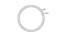
これらの反応ガスは、従来法のようにクランプリングを接触させただけではウエハWの裏面側への周り込みを抑制する効果が十分でなく、図1(a)に示すようにウエハWの側面や裏面に膜101が成膜されてしまう場合がある。
Before describing a specific configuration of a film forming apparatus according to an embodiment of the present invention, a reaction gas having high permeability to a gap between members and a problem when this reaction gas is used will be described.
The inventor forms, for example, a metal film of ruthenium (Ru) or nickel (Ni) or an oxide film of these oxides (RuO 2 , RuO 4 , NiO, Ni 2 O 3 , NiO 2, etc.). It has been found that some of the reaction gases used as the metal source have high permeability between members. These films are used as electrodes and insulating films of semiconductor devices.
These reaction gases are not sufficient in suppressing the wrapping around the back surface of the wafer W only by contacting the clamp ring as in the conventional method, and the side surface of the wafer W as shown in FIG. In other cases, the
特に、RuやNiの金属膜やその酸化膜に対しては、成膜後の後段の処理にて、例えば酸素雰囲気下で膜101の表面にパッシベーション膜102を成膜し(図1(b))、次いで水素ガス雰囲気などの還元雰囲気下で加熱処理などを行うことがある(図1(c))。このとき、パッシベーション膜102が形成されないウエハWの側面や裏面に形成された膜101は、酸素雰囲気に晒されることにより、少なくともその表面に酸化物が形成され、次いで還元雰囲気に晒されることによりこの酸化物が還元されて金属になる。このように還元されて生成した金属は、特に粉化しやすく、搬送アームなどと接触して汚染源となるおそれが高い。
In particular, for a Ru or Ni metal film or its oxide film, a
そこで、本発明者は、ウエハWの裏面への反応ガスの回り込みを抑える効果が従来よりも高いクランプリング5を備える成膜装置を開発した。以下、Ruの酸化膜を成膜する例を挙げて、実施の形態に関わる成膜装置について説明する。
本例の成膜装置は、Ruを含む反応ガス(以下、Ruソースという)と、酸化ガスである酸素ガスとを反応させて、ALD法により、例えば直径300mmのウエハ表面に酸化ルテニウム(RuO2)の薄膜を成膜する。
In view of this, the present inventor has developed a film forming apparatus provided with a
In the film forming apparatus of this example, a reaction gas containing Ru (hereinafter referred to as Ru source) and an oxygen gas which is an oxidizing gas are reacted, and ruthenium oxide (RuO 2) is formed on a wafer surface having a diameter of 300 mm, for example, by ALD. ).
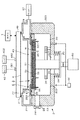
図2の縦断面図に示すように、この成膜装置は、内部に真空雰囲気が形成される処理容器2と、当該処理容器2内に設けられ、ウエハWを載置するための載置台3と、この載置台3と対向するように処理容器2の上部に設けられ、ウエハW表面に処理ガスを供給するためのガスシャワーヘッド4と、を備えている。
As shown in the longitudinal sectional view of FIG. 2, this film forming apparatus includes a
載置台3は、ウエハWを支持するステージ31と、このステージ31を覆うステージカバー32と、から構成されており、ステージ31は例えば窒化アルミニウムや石英などを材料として、扁平な円板状に形成されている。ステージ31の内部には、載置台3の載置面を加熱することにより、ウエハWを成膜温度まで昇温するための基板加熱部であるステージヒーター33が埋設されている。このステージヒーター33は、例えばシート状の抵抗発熱体より構成されていて、不図示の電源部から電力を供給することにより載置台3上に載置されたウエハWを例えば250℃に加熱することができる。またステージ31内には図示しない静電チャックが設けられており、載置台3上に載置されたウエハWを静電吸着して固定することができる。なお、図2、図11以外の図では、ステージヒーター33の記載は省略してある。
The mounting table 3 includes a
ステージ31と共に載置台3を構成するステージカバー32は、ステージ31の上面及び側面を覆うことにより、反応生成物や反応副生成物といった反応物のステージ31表面への堆積を防止する。ステージカバー32は例えば石英製の着脱自在なカバー部材(デポシールドなどと呼ばれている)として構成されており、その上面側の中央領域には、ウエハWよりやや大きな径を有する円形の凹部が形成されていて、当該ステージカバー32上の載置面に載置されるウエハWの位置決めを行うことができる。
The stage cover 32 that constitutes the stage 3 together with the
載置台3は、柱状の支持部材34によって例えばステージ31の下面側中央部を支持されており、当該支持部材34は昇降機構69によって昇降されるように構成されている。そしてこの支持部材34を昇降させることにより載置台3は、外部のウエハ搬送機構との間でウエハWの受け渡しが行われる受け渡し位置と、ウエハWの処理が行われる処理位置と、の間を昇降することができる。
The mounting table 3 is supported by a
図2に示すように支持部材34は、処理容器2の底面部、詳しくは後述の下側容器22の底面部を貫通し、既述の昇降機構69によって昇降される昇降板23に接続されていると共に、この昇降板23と下側容器22との間はベローズ24によって気密に接合されている。
As shown in FIG. 2, the
また載置台3は、ウエハWの裏面を支えて当該ウエハWを載置台3の載置面より昇降させるための例えば3本の昇降ピン35を備えている。これらの昇降ピン35は、例えば図2に示すように載置台3をウエハWの処理位置まで移動させた状態で、各昇降ピン35の扁平な頭部がステージ31の上面にて係止され、その下端部がステージ31の底面から飛び出すように、ステージ31を上下方向に貫通している。
The mounting table 3 includes, for example, three lifting
ステージ31を貫通した各昇降ピン35の下方側には、リング状の昇降部材36が設けられていて、載置台3をウエハWの受け渡し位置まで降下させた状態で昇降部材36を昇降させ、各昇降ピン35を押し上げたり降下させたりすることにより、これら昇降ピン35に支持されたウエハWを載置台3の載置面より昇降させることができる(図5参照)。
A ring-shaped elevating
ここでステージカバー32の上面側における、既述の昇降ピン35が貫通している位置には、昇降ピン35の頭部を格納するための開口部が設けられている。このため、図2に示すようにウエハWの処理位置まで載置台3を移動させた状態では、昇降ピン35の頭部が開口部内に収容され、載置台3の上面に平坦なウエハWの載置面が形成される。さらに当該ステージカバー32の側壁部は、ステージ31の下方側まで延伸されていて、ステージ31の下方領域を側面から取り囲むスカート部321を形成している。
Here, on the upper surface side of the
次に処理容器2の構成について説明する。処理容器2は、扁平な椀形の下側容器22の上に環状に形成された排気ダクト21を積み重ねた構成となっている。下側容器22は、例えばアルミニウムなどにより構成され、その底面には貫通孔221が設けられていて、既述したステージ31の支持部材34を貫通させる。また当該貫通孔221の周囲には、例えば4箇所にパージガス供給路222が設けられていて、パージガス供給源66から供給された窒素ガスなどのパージガスを載置台3下方側の空間(後述のボトムエリア20)に供給することができる。パージガス供給路222やパージガス供給源66は、本例のパージガス供給部に相当する。
下側容器22の側壁部223には、外部のウエハ搬送機構によりウエハWの搬入出を行うための搬入出口28が設けられており、この搬入出口28はゲートバルブ281によって開閉される。
Next, the configuration of the
A loading / unloading
排気ダクト21は、例えばアルミニウム製の角状のダクトを湾曲させて形成された環状体として構成されており、下側容器22の上に積み重ねられて処理容器2を構成している。当該排気ダクト21の内周側の面は、載置台3の上方側の領域へ向けて開口している。当該排気ダクト21の外壁面には排気管29が接続されていて、当該排気管29に接続された真空ポンプ67を利用して、処理容器2内の真空排気を行うことができる。これら排気管29や真空ポンプ67は、本例の排気部に相当する。
The
さらに処理容器2には、処理位置の載置台3を囲み、処理容器2の内部を上部側の処理空間40と下部側の空間であるボトムエリア20とに分ける囲み部材であるインナーリング26が設けられている。このインナーリング26は、例えばアルミニウムにより形成されたリング状部材であって、下側容器22の側壁部223の内壁面と、載置台3の側周面との間に装填できる形状に形成されている。インナーリング26の上面外周部には、当該外側へ向けて広がるようにフランジ部263が設けられており、インナーリング26は、前記排気ダクト21にこのフランジ部263を係止させた状態で処理容器2内に配置されている。また、インナーリング26は例えば石英製のリングカバーによりその上面側を覆ってもよい。
Further, the
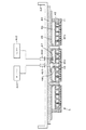
次にガスシャワーヘッド4の構成について説明する。図3に示すようにガスシャワーヘッド4は、扁平なリング状の側壁部42と、この側壁部42を上下から覆う天板43及び底板41とによって囲まれる空間内に円板状の隔壁部44を設けて、当該空間を上部空間45と下部空間46とに上下に区画した構造となっている。
Next, the configuration of the
下部空間46は、上部空間45を貫通するRuソース供給路480を介してRuソース供給管481に接続されており、Ruソース供給管481の上流側には、Ruソースを貯留する原料タンクや気化器、流量調節部などを備えたRuソース供給部401が設けられている。また、Ruソース供給路480は、不図示のパージガス供給部にも接続されており、窒素ガスなどのパージガスを下部空間46に供給することもできる。Ruソース供給路480を介して下部空間46に供給されたRuソースやパージガスは、下部空間46内に拡散し、底板41の全面に設けられたガス供給孔461を介して処理空間40に供給される。
The
上部空間45は、天板43の下面に設けられた酸化ガス供給部47を介して酸化ガス供給管482に接続され、酸化ガス供給管482の上流側には、酸素タンクや流量調節部などを備えた酸化ガス供給部402が設けられている。酸化ガス供給部47を介して上部空間45に供給された酸素ガスは、上部空間45内に拡散し、隔壁部44、下部空間46、底板41を貫通するように設けられたガス供給孔451を通って底板41の全面から処理空間40に供給される。
The
上述のようにガスシャワーヘッド4は、Ruソースと酸素ガスとを異なる流路から供給することにより、両ガスの反応による堆積物の堆積を防止する構造となっているが、反応ガスを供給する手法はこれに限られるものではない。例えば、これらRuソースや酸素ガスを共通の流路から処理空間40へと供給してもよい。この場合には、反応ガスの切り替え時に当該流路内に窒素ガスなどのパージガスを供給し、Ruソースと酸素ガスとが混在しないようにしてガスシャワーヘッド4内の堆積物の堆積を防止するとよい。
As described above, the
ガスシャワーヘッド4は、支持部材49により上面側から支持され、排気ダクト21の上面側の開口を当該支持部材49によって塞ぐことにより、処理容器2が密閉される。排気ダクト21と支持部材49との間には、処理容器2内を気密に保つためのOリング211が設けられている。
支持部材49によって支持されたガスシャワーヘッド4は、その底面が載置台3の上面と対向するように配置され、これらガスシャワーヘッド4と載置台3との間の処理空間40に反応ガスが供給されてウエハWに対する成膜処理が行われる。
The
The
また、ガスシャワーヘッド4と排気ダクト21との間には、この空間の通流コンダクタンスを小さくすることにより、処理空間40からみて処理容器2の周方向における排気の均一化を計るための円筒形状のバッフルリング27が下方側に向けて伸び出している。
In addition, a cylindrical shape is provided between the
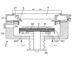
さらに本例の成膜装置は、載置台3に載置されたウエハWの下面側への反応ガスの周り込みを抑えるためのクランプリング5が設けられている。図2、図4示すように、クランプリング5は、円環状の板材からなる本体部51を備え、この本体部51の下面をインナーリング26上に載置した状態で処理容器2内に配置されている。本体部51の内縁部52はインナーリング26の内周面よりもさらに内側へ向けて伸び出しており、その内端は載置台3上に載置されたウエハWの周縁部の上方に位置している。
Further, the film forming apparatus of this example is provided with a
本例のクランプリング5は、インナーリング26上に載置されているとき、内縁部52の内端が、インナーリング26の上面よりも下方側に伸び出している。また、当該内端の下面には、平坦な当接面521が形成されており、載置台3上のウエハWの周縁部に全周に亘ってこの当接面521を当接させることができる。
When the
本体部51の下面には、クランプリング5の周方向に沿って筒状に形成された筒状壁部54が設けられている。図8に示すように、筒状壁部54は、処理位置に位置する載置台3とインナーリング26との間に位置するように配置される。
A
さらに本体部51の下面側には、位置決めのための複数個の凸部53が設けられており凸部53は、インナーリング26の上面側に設けられた凹部267(図8参照)に挿入されてインナーリング26上におけるクランプリング5の載置位置が定められる。
クランプリング5はアルミニウムなどの金属により構成してもよいし、アルミナなどのセラミックにより構成してもよい。クランプリング5は載置台3上のウエハWに対して当接面521を押し当てることにより反応ガスの回り込みを抑えるのに十分な重量、例えば数百グラム〜数キログラム程度の重量を有している。
Further, a plurality of
The
また、インナーリング26には、本体部51がウエハWに当接したときに、ステージヒーター33からの熱を受けて熱膨張することにより、当接面521とウエハWとが擦れ合い、ウエハWが削れてパーティクルが発生しないようにするために、クランプリング5を予熱する予熱部である複数本のシースヒーター264が設けられている。図4に示すように本例のインナーリング26は、上部部材262と下部部材261とをボルト265によって上下に締結して構成されており、前記シースヒーター264は、これら下部部材261、上部部材262の接合面に沿って形成された溝部内に配設されている。各シースヒーター264は不図示の電源部から電力を供給することによりインナーリング26を介してクランプリング5を加熱する。クランプリング5の加熱温度は、シースヒーター264からの熱の供給がなくなった後に、クランプリング5の温度が載置台3上のウエハWの温度とほぼバランスする程度の温度、例えば280℃に調節されている。
Further, when the
また、図4に示すように、インナーリング26の下部部材261には、その内周面を下方側向けて延伸するように突出する円筒状の突出部266が設けられており、筒状壁部54を囲む面積を大きくしている。
As shown in FIG. 4, the
以上に説明した構成を備える成膜装置は、Ruソース供給部401や酸化ガス供給部402からの反応ガス等の供給動作、載置台3の昇降動作や真空ポンプ67による処理容器2内の排気動作、ステージヒーター33、やシースヒーター264による加熱動作などを制御する制御部7を備えている。制御部7は例えば図示しないCPUと記憶部とを備えたコンピュータからなり、この記憶部には上述の各動作を実行するためのステップ(命令)群が組まれたプログラムが記録されている。このプログラムは、例えばハードディスク、コンパクトディスク、マグネットオプティカルディスク、メモリカードなどの記憶媒体に格納され、そこから記憶部にインストールされる。
The film forming apparatus having the above-described configuration is configured to supply a reaction gas or the like from the Ru
以下、本成膜装置の作用について図5〜図8を参照しながら説明する。予め処理容器2内を真空雰囲気に減圧した後、図5に示すように載置台3を受け渡し位置まで降下させる。そして、ゲートバルブ281を開放し、搬入出口28と接続された真空搬送室に設けられたウエハ搬送機構の搬送アームを進入させ、昇降ピン35との間でウエハWの受け渡しを行う。しかる後、昇降ピン35を降下させ、ステージヒーター33によって加熱された載置台3上にウエハWを載置する。
Hereinafter, the operation of the film forming apparatus will be described with reference to FIGS. After reducing the inside of the
次いで、ゲートバルブ281を閉じ、載置台3を処理位置まで上昇させる。既述のようにインナーリング26上に載置された状態においてクランプリング5の内縁部52は、当接面521がインナーリング26の上面よりも下方側に位置するように伸び出している。
Next, the
このため図8に示すように、載置台3を処理位置まで上昇させると、インナーリング26の上面よりも下方側に伸び出しているクランプリング5の当接面521がウエハWの周縁部に全周に亘って当接し、クランプリング5がインナーリング26の上面から持ち上げられる。これにより前記当接面521にクランプリング5の自重が加えられ、クランプリング5がウエハWに密着した状態となる。
For this reason, as shown in FIG. 8, when the mounting table 3 is raised to the processing position, the
また、このときクランプリング5がシースヒーター264によって予熱されていることにより、クランプリング5がインナーリング26から持ち上げられた後、ステージヒーター33によって加熱されているウエハWの温度と、このウエハW上に載置されたクランプリング5の温度とがほぼバランスする。この結果、クランプリング5の熱膨張が抑えられ、クランプリング5とウエハWとの擦れ合いによるパーティクルの発生を抑制することができる。
At this time, since the
しかる後、処理容器2内の圧力調整を行った後、Ruソース供給部401よりRuソースを供給する(図6)。ガスシャワーヘッド4に供給されたRuソースは、下部空間46内を広がり、ガス供給孔461を介して処理空間40内の全体に向けて下方側へ吐出される。処理空間40に吐出されたRuソースは、載置台3上のウエハWへ向けて流下し、その表面に達するとRuソースはウエハWに吸着する。
Then, after adjusting the pressure in the
ウエハWに到達したRuソースは、ウエハWの表面に沿って径方向に放射状に広がり、バッフルリング27とクランプリング5との隙間を介し、処理空間40から排気ダクト21へ向けて流れ出す。排気ダクト21内に流れ込んだRuソースは、排気管29を介して外部へ排気される。
The Ru source that has reached the wafer W spreads radially along the surface of the wafer W and flows out from the
このように、ウエハWの表面を放射状に広がるRuソースは、図8に示すようにウエハWの周縁部の上方を通過する。しかしながら当該周縁部には、クランプリング5の内縁部52がその全周に亘って当接していると共に、この当接面521にはクランプリング5の自重が加わっている。このため、当該当接面521とウエハWとが十分に密着し、浸透性の高いRuソースであってもこれらの部材(当接面521、ウエハW)の間には殆ど入り込むことができない。この結果、ウエハWの表面側を流れるRuソースがウエハWの側面や裏面側に流れ込んで吸着する現象の発生を抑えることができる。
In this way, the Ru source that spreads radially on the surface of the wafer W passes above the peripheral edge of the wafer W as shown in FIG. However, the
一方、載置台3によって持ち上げられたクランプリング5の下面とインナーリング26の上面との間には、隙間が形成され、この隙間を介してRuソースが載置台3側に進入するおそれもある。そこでクランプリング5の下面側に、インナーリング26と載置台3との間に位置する筒状壁部54を設けることにより、クランプリング5の外縁部から内縁部52までの連通空間の距離を長くして、ウエハWの側面や裏面側へのRuソースガスの到達を阻んでいる。さらに、ボトムエリア20に供給されたパージガスが、インナーリング26の内周面と筒状壁部54の外周面との隙間、及びクランプリング5の下面とインナーリング26の上面との隙間を流れて排気ダクト21へと排出される流れが形成される。このパージガスの流れが形成されることにより、クランプリング5の外縁部から下面側に進入したRuソースを押し戻すこともできる。
On the other hand, a gap is formed between the lower surface of the
クランプリング5を利用してウエハWの裏面側への回り込みを抑えながら、ウエハWの表面にRuソースを供給し、所定時間が経過したら、Ruソースの供給を停止し、下部空間46内のRuソースを窒素ガスによりパージする(図6)。
The Ru source is supplied to the front surface of the wafer W while suppressing the wraparound to the back side of the wafer W using the
しかる後、酸化ガス供給部402からガスシャワーヘッド4に酸素ガスを供給する(図7)。ガスシャワーヘッド4に供給された酸素ガスは、上部空間45内を広がり、ガス供給孔451を介して処理空間40内の全体に向けて下方側へ吐出される。処理空間40に吐出された酸素ガスは、載置台3上のウエハWへ向けて流下し、その表面に達するとウエハWの表面に吸着しているRuソースと反応してRuO2の分子層が形成される。酸素ガスの供給開始後、所定時間が経過したら、酸素ガスの供給を停止し、上部空間45内の酸素ガスを窒素ガスによりパージする(図7)。
Thereafter, oxygen gas is supplied from the oxidizing
ウエハWに到達した酸素ガスは、既述のRuソースと同様の流れを形成し、排気ダクト21へ向けて流れていくが、ウエハWの周縁部はクランプリング5によって覆われている。また、クランプリング5の下面には、クランプリング5の外縁部側からウエハWへの酸素ガスの進入を妨げる筒状壁部54が設けられ、さらにクランプリング5とインナーリング26との隙間に進入した酸素ガスを押し戻すパージガスの流れが形成されている。これらの作用により、載置台3上のウエハWの裏面側への酸素ガスの回り込みも抑えられ、ウエハWの側面や裏面へのRuO2の形成が抑えられる。
The oxygen gas that has reached the wafer W forms a flow similar to that of the Ru source described above and flows toward the
以上に説明した工程を繰り返し、処理空間40にRuソースと酸素ガスとを交互に供給することにより、ウエハWの表面にRuO2の分子層が積層され、RuO2の膜101が成膜される。
こうしてRuソースの供給と酸素ガスの供給とを例えば数十回〜数百回繰り返し、所望の膜厚の膜101を成膜したら、載置台3を受け渡し位置まで降下させる。そしてゲートバルブ281を開いて搬送アームを進入させ、搬入時とは逆の手順で昇降ピン35から搬送アームにウエハWを受け渡し、成膜後のウエハWを搬出させた後、次のウエハWの搬入を待つ。
By repeating the steps described above and alternately supplying Ru source and oxygen gas to the
Thus, the Ru source supply and the oxygen gas supply are repeated, for example, several tens to several hundreds of times, and when the
本実施の形態に係わる成膜装置によれば以下の効果がある。載置台3上に載置されたウエハWの周縁部の全周に亘って当接する内縁部52を備えたクランプリング5を用い、載置台3によって内縁部52の当接面521を介してこのクランプリング5を持ち上げることによりクランプリング5をウエハWに密着させるので、当該ウエハWの裏面への反応ガス(Ruソースのガス、酸素ガス)の回り込みが効果的に抑えられる。
The film forming apparatus according to the present embodiment has the following effects. A
さらに前記クランプリング5には、その下方側向けて伸び出す筒状の筒状壁部54が設けられ、載置台3とインナーリング26との間にこの筒状壁部54が位置している。この結果、クランプリング5の下面側を介した反応ガスの進入が阻まれ、ウエハWの裏面への反応ガスの回り込みを抑えることができる。
Further, the
以上に説明した成膜装置によれば、図9(a)に模式的に示すようにクランプリング5を用いて成膜を行うことにより、ウエハWの側面及び裏面への膜101の形成を抑えることができる。この結果、膜101の表面にパッシベーション膜102を形成する際に、このパッシベーション膜102によって覆われていない領域が殆ど発生しない(図9(b))。膜101の全面がパッシベーション膜102で覆われていることにより、還元雰囲気下(例えば水素ガス雰囲気)で加熱処理などを行っても、当該膜101が還元雰囲気に晒されず、粉化しやすい金属の形成を抑えることができるという効果がある(図9(c))。
According to the film forming apparatus described above, film formation is performed using the
図10は、囲み部材であるインナーリング26aと載置台3との間に位置する筒状壁部54を外周側から周方向に囲むように、クランプリング5aの下面から下方側に伸び出す、一つ、または複数の外筒壁部541を設けた例を示している(図10には、複数の外筒壁部541を設けた例を示してある)。インナーリング26aの上面には、これらの外筒壁部541を挿入するための溝部268が形成されている。そして、載置台3によりこのクランプリング5aを持ち上げると、外筒壁部541と溝部268との間にラビリンスシールが形成される。これによりクランプリング5aの外縁部側からの反応ガスの進入を妨げる効果がさらに向上する。
なお、以下に説明する各例では、図2〜図4に示した成膜装置と共通の構成要素には、これらの図と同じ符号を付してある。
FIG. 10 shows that the
In each example described below, the same reference numerals as those in these drawings are attached to the same components as those of the film forming apparatus shown in FIGS.
次に、本発明の第2の実施の形態に関わる成膜装置について図11〜図13を用いて説明する。第2の実施の形態に関わる成膜装置は、クランプリング5の下面に筒状壁部54を設けることに代えて、囲み部材であるインナーリング26bからクランプリング5bと載置台3との間に向けて伸び出す案内部269を設けた点が第1の実施の形態の成膜装置と異なる。
Next, a film forming apparatus according to the second embodiment of the present invention will be described with reference to FIGS. In the film forming apparatus according to the second embodiment, instead of providing the
図12に示すように、案内部269は、クランプリング5bの下面に沿って、インナーリング26bの上端部から内側へ向けて伸び出している。案内部269の先端は、載置台3の周縁部を上面側から覆うように、載置台3上に載置されるウエハWの周縁部の近傍位置まで伸び出している。また、クランプリング5bがインナーリング26b上に載置されている状態において、クランプリング5bの内端の平坦な当接面521の高さ位置は、案内部269の下面よりも低い位置にある。そして図13に示すように、載置台3を処理位置に位置させると、ウエハWを介して載置台3によってクランプリング5bがインナーリング26bから持ち上げられてこれらの部材5b、26bに隙間が形成されると共に、この隙間に案内部269が配置される。この結果、当該案内部269の上下面側には、ボトムエリア20に供給されたパージガスが通流する流路が形成される。
As shown in FIG. 12, the
この流路に沿ってパージガスを通流させることにより、パージガスは、案内部269に案内されて載置台3上のウエハWの側方を通過して処理空間40へと流れ込む。ウエハWの側方にパージガスの流れが形成されることにより、クランプリング5bの外縁部側から反応ガスが進入したとしても、当該パージガスによって反応ガスが押し戻される。特に、案内部269の先端が載置台3上のウエハWの近傍位置まで伸び出していることにより、ウエハWの近くまで進入した反応ガスのパージガスによる置換が進むと共に、ウエハWの裏面近傍に反応ガスが滞留しにくくなる。これらの相乗効果によりウエハWの裏面への反応ガスの回り込みが効果的に抑えられる。
By causing the purge gas to flow along this flow path, the purge gas is guided by the
以上に説明したように本成膜装置に設けられているクランプリング5、5a、5bは、浸透性の高い反応ガスの侵入を抑える効果がある。従って、RuやNiを含む金属ソースほどは浸透性の高くない金属ソースを反応ガスとして、成膜を行う場合にも同等以上の効果を発揮することができる。 As described above, the clamp rings 5, 5 a, 5 b provided in the film forming apparatus have an effect of suppressing invasion of a reaction gas having high permeability. Therefore, when a film is formed using a metal source that is less permeable than a metal source containing Ru or Ni as a reaction gas, the same or higher effect can be exhibited.
このような金属ソースの例として、例えば周期表の第3周期の元素であるAl、Si等、周期表の第4周期の元素であるTi、Cr、Mn、Fe、Co、Cu、Zn、Ge等、周期表の第5周期の元素であるZr、Mo、Rh、Pd、Ag等、周期表の第6周期の元素であるBa、Hf、Ta、W、Re、lr、Pt等の元素を含む反応ガスを用いてこれらの金属やその酸化物の膜を成膜する場合を例示できる。ウエハW表面に吸着させる金属ソースとしては、これらの金属元素の有機金属化合物や無機金属化合物などを反応ガスとして用いる場合が挙げられる。 Examples of such a metal source include Ti, Cr, Mn, Fe, Co, Cu, Zn, Ge, which are elements of the fourth period of the periodic table, such as Al and Si, which are elements of the third period of the periodic table. Etc., elements such as Zr, Mo, Rh, Pd, and Ag that are elements of the fifth period of the periodic table, and elements such as Ba, Hf, Ta, W, Re, lr, and Pt that are elements of the sixth period of the periodic table. A case where a film of these metals or an oxide thereof is formed using a reaction gas containing the gas can be exemplified. Examples of the metal source to be adsorbed on the surface of the wafer W include a case where an organic metal compound or an inorganic metal compound of these metal elements is used as a reaction gas.
また、ウエハWの表面に吸着した原料ソースを反応させて、所望の膜を得る反応には、例えばO2、O3、H2O等を利用した酸化反応、H2、HCOOH、CH3COOH等の有機酸、CH3OH、C2H5OH等のアルコール類等を利用した還元反応、CH4、C2H6、C2H4、C2H2等を利用した炭化反応、NH3、NH2NH2、N2等を利用した窒化反応等の各種反応を利用してもよい。 Further, for the reaction to obtain a desired film by reacting the raw material source adsorbed on the surface of the wafer W, for example, an oxidation reaction using O 2 , O 3 , H 2 O, etc., H 2 , HCOOH, CH 3 COOH Reduction reaction using alcohols such as organic acids such as CH 3 OH, C 2 H 5 OH, etc., carbonization reaction using CH 4 , C 2 H 6 , C 2 H 4 , C 2 H 2 etc., NH 3 , various reactions such as a nitriding reaction using NH 2 NH 2 , N 2 or the like may be used.
さらに、反応ガスとして、3種類の反応ガスや4種類の反応ガスを用いてもよい。
一方で、ウエハWの表面に膜101を成膜する手法は、ALD法に限られるものではない。例えば金属ソースを処理容器2内に連続的に供給し、ウエハWの加熱されたウエハWの表面で金属ソースを分解させて薄膜を得る熱CVD法や、金属ソースと反応ガスなどをプラズマの存在下で活性化して反応させ連続的な成膜を行うプラズマCVD法などの各種のCVD法にも本発明は適用することができる。
Further, three types of reactive gases or four types of reactive gases may be used as the reactive gases.
On the other hand, the method of forming the
(実験)
クランプリング5を用いた場合と、クランプリング5を用いない場合とでウエハWの裏面側への反応ガスの回り込みを比較した。
A.実験条件
(実施例) 図2に示したものと同様の構成を備える成膜装置を用いて、ウエハWの表面にRuソースと酸素ガスを交互に供給し、RuO2膜の成膜を行った。
(比較例)クランプリング5が設けられていない成膜装置を用いて実施例と同様の条件下でRuO2膜の成膜を行った。
(Experiment)
The reaction gas wraparound to the back side of the wafer W was compared between the case where the
A. Experimental conditions
Example A RuO 2 film was formed by alternately supplying Ru source and oxygen gas to the surface of the wafer W using a film forming apparatus having the same configuration as that shown in FIG.
(Comparative Example) A RuO 2 film was formed under the same conditions as in the example using a film forming apparatus in which the
B.実験結果
実施例の結果によれば、ウエハWの裏面側にはRuO2膜の成膜は確認されなかった。一方、比較例の結果によれば、図14に模式的に示すように、ウエハWの裏面側にリング状にRuO2の膜101が成膜された。これにより、本例のクランプリング5を用いることにより、浸透性の高いRuソースであっても反応ガスのウエハWの裏面側への回り込みを抑えることができることを確認できた。
B. Experimental Results According to the results of the examples, no RuO 2 film was formed on the back side of the wafer W. On the other hand, according to the result of the comparative example, a RuO 2 film 101 was formed in a ring shape on the back side of the wafer W as schematically shown in FIG. Thus, it was confirmed that by using the
W ウエハ
2 処理容器
26、26a、26b
インナーリング
264 シースヒーター
3 載置台
40 処理空間
5、5a、5b
クランプリング
52 内縁部
54 筒状壁部
541 外筒壁部
Claims (6)
基板を載置するために前記処理容器内に設けられ、成膜処理が行われる処理位置と、この処理位置の下方側であって、外部との間で基板の受け渡しが行われる受け渡し位置との間で昇降自在に構成された載置台と、
前記処理位置の載置台を囲み、前記処理容器の内部を、前記反応ガスが供給される上部側の処理空間と、下部側の空間とに分ける囲み部材と、
前記処理空間側から前記処理容器内の真空排気を行う排気部と、
前記載置台が受け渡し位置にあるときには前記囲み部材の上面に載置されると共に、当該載置台が処理位置に上昇したときにはその内縁部が前記載置台上の基板の周縁部に全周に亘って当接して前記囲み部材の上面から持ち上げられ、基板の裏面側への反応ガスの回り込みを防止するためのクランプリングと、
前記囲み部材の上面に載置される領域を含むクランプリングの下面から下方側に向けて伸び出すと共に、当該クランプリングの周方向に沿って筒状に形成され、前記載置台の外周面と、前記囲み部材の内周面との間に位置する筒状壁部と、を備え、
前記クランプリングの下面にて、前記筒状壁部は、当該クランプリングが囲み部材の上面から持ち上げられたとき、前記囲み部材の上面とクランプリングの下面との間に横向きの隙間が形成され、且つ、前記囲み部材の内周面と筒状壁部の外周面との間に、前記囲み部材−クランプリング間の横向きの隙間と連通する縦向きの隙間が形成されると共に、前記内縁部が基板の周縁部に当接する位置よりも外側のクランプリングの下面と、前記載置台の上面との間に横向きの隙間が形成され、且つ、前記載置台の外周面と筒状壁部の内周面との間に、前記クランプリング−載置台間の横向きの隙間と連通する縦向きの隙間が形成される位置に設けられていることを特徴とする成膜装置。 In a film forming apparatus that performs a film forming process by supplying a reactive gas to a substrate in a processing container in a vacuum atmosphere,
A processing position that is provided in the processing container for placing the substrate and a film forming process is performed, and a transfer position that is below the processing position and that transfers the substrate to and from the outside. A mounting table configured to freely move up and down,
A surrounding member that surrounds the mounting table at the processing position and divides the inside of the processing container into an upper processing space to which the reaction gas is supplied and a lower space;
An exhaust section for evacuating the processing container from the processing space side;
When the mounting table is at the transfer position, it is placed on the upper surface of the surrounding member, and when the mounting table is raised to the processing position, the inner edge of the mounting table extends to the peripheral edge of the substrate on the mounting table. A clamp ring that comes into contact with and is lifted from the upper surface of the surrounding member, and prevents the reaction gas from wrapping around the back surface of the substrate;
And extending downward from the lower surface of the clamp ring including the region placed on the upper surface of the surrounding member, and is formed in a cylindrical shape along the circumferential direction of the clamp ring, and the outer peripheral surface of the mounting table, A cylindrical wall portion located between the inner peripheral surface of the surrounding member,
At the lower surface of the clamp ring, when the clamp ring is lifted from the upper surface of the surrounding member, a lateral gap is formed between the upper surface of the surrounding member and the lower surface of the clamp ring. In addition, a vertical gap is formed between the inner peripheral surface of the surrounding member and the outer peripheral surface of the cylindrical wall portion so as to communicate with the lateral gap between the surrounding member and the clamp ring , and the inner edge portion is A lateral gap is formed between the lower surface of the clamp ring outside the position in contact with the peripheral edge of the substrate and the upper surface of the mounting table, and the outer peripheral surface of the mounting table and the inner periphery of the cylindrical wall portion A film forming apparatus , wherein a vertical gap that communicates with a horizontal gap between the clamp ring and the mounting table is formed between the surface and the surface.
基板を載置するために前記処理容器内に設けられ、成膜処理が行われる処理位置と、この処理位置の下方側であって、外部との間で基板の受け渡しが行われる受け渡し位置との間で昇降自在に構成された載置台と、
前記処理位置の載置台を囲み、前記処理容器の内部を、前記反応ガスが供給される上部側の処理空間と、下部側の空間とに分ける囲み部材と、
前記処理空間側から前記処理容器内の真空排気を行う排気部と、
前記下部側の空間にパージガスを供給するパージガス供給部と、
前記載置台が受け渡し位置にあるときには前記囲み部材の上面に載置されると共に、当該載置台が処理位置に上昇したときにはその内縁部が前記載置台上の基板の周縁部に全周に亘って当接して前記囲み部材の上面から持ち上げられ、基板の裏面側への反応ガスの回り込みを防止するためのクランプリングと、
前記処理位置にある載置台の上面と前記クランプリングの下面との間に伸び出すように前記囲み部材に設けられ、前記パージガス供給部から供給されたパージガスが前記載置台上の基板の側方を通過して処理空間へと流れ込むように、パージガスの流れを案内する案内部と、を備えることを特徴とする成膜装置。 In a film forming apparatus that performs a film forming process by supplying a reactive gas to a substrate in a processing container in a vacuum atmosphere,
A processing position that is provided in the processing container for placing the substrate and a film forming process is performed, and a transfer position that is below the processing position and that transfers the substrate to and from the outside. A mounting table configured to freely move up and down,
A surrounding member that surrounds the mounting table at the processing position and divides the inside of the processing container into an upper processing space to which the reaction gas is supplied and a lower space;
An exhaust section for evacuating the processing container from the processing space side;
A purge gas supply section for supplying a purge gas to the lower space;
When the mounting table is at the transfer position, it is placed on the upper surface of the surrounding member, and when the mounting table is raised to the processing position, the inner edge of the mounting table extends to the peripheral edge of the substrate on the mounting table. A clamp ring that comes into contact with and is lifted from the upper surface of the surrounding member, and prevents the reaction gas from wrapping around the back surface of the substrate;
The enclosure member is provided so as to extend between the upper surface of the mounting table at the processing position and the lower surface of the clamp ring, and the purge gas supplied from the purge gas supply unit passes the side of the substrate on the mounting table. A film forming apparatus comprising: a guide unit that guides a flow of purge gas so as to pass through and flow into the processing space.
Priority Applications (4)
| Application Number | Priority Date | Filing Date | Title |
|---|---|---|---|
| JP2012251595A JP6056403B2 (en) | 2012-11-15 | 2012-11-15 | Deposition equipment |
| KR1020130133015A KR101751094B1 (en) | 2012-11-15 | 2013-11-04 | Film forming apparatus |
| US14/074,302 US10094019B2 (en) | 2012-11-15 | 2013-11-07 | Film forming apparatus |
| US15/243,048 US10526702B2 (en) | 2012-11-15 | 2016-08-22 | Film forming apparatus |
Applications Claiming Priority (1)
| Application Number | Priority Date | Filing Date | Title |
|---|---|---|---|
| JP2012251595A JP6056403B2 (en) | 2012-11-15 | 2012-11-15 | Deposition equipment |
Publications (2)
| Publication Number | Publication Date |
|---|---|
| JP2014098202A JP2014098202A (en) | 2014-05-29 |
| JP6056403B2 true JP6056403B2 (en) | 2017-01-11 |
Family
ID=50680438
Family Applications (1)
| Application Number | Title | Priority Date | Filing Date |
|---|---|---|---|
| JP2012251595A Active JP6056403B2 (en) | 2012-11-15 | 2012-11-15 | Deposition equipment |
Country Status (3)
| Country | Link |
|---|---|
| US (2) | US10094019B2 (en) |
| JP (1) | JP6056403B2 (en) |
| KR (1) | KR101751094B1 (en) |
Families Citing this family (38)
| Publication number | Priority date | Publication date | Assignee | Title |
|---|---|---|---|---|
| US11437269B2 (en) | 2012-03-27 | 2022-09-06 | Novellus Systems, Inc. | Tungsten feature fill with nucleation inhibition |
| JP6038698B2 (en) * | 2013-03-22 | 2016-12-07 | 日本碍子株式会社 | Ceramic member and member for semiconductor manufacturing equipment |
| JP6007143B2 (en) * | 2013-03-26 | 2016-10-12 | 東京エレクトロン株式会社 | Shower head, plasma processing apparatus, and plasma processing method |
| WO2015084487A1 (en) * | 2013-12-06 | 2015-06-11 | Applied Materials, Inc. | Apparatus for self centering preheat member |
| KR101560623B1 (en) * | 2014-01-03 | 2015-10-15 | 주식회사 유진테크 | Substrate processing apparatus and substrate processing method |
| CN105336655A (en) * | 2014-06-12 | 2016-02-17 | 北京北方微电子基地设备工艺研究中心有限责任公司 | Bearing apparatus and semiconductor processing device |
| US10167552B2 (en) * | 2015-02-05 | 2019-01-01 | Lam Research Ag | Spin chuck with rotating gas showerhead |
| US9963782B2 (en) * | 2015-02-12 | 2018-05-08 | Asm Ip Holding B.V. | Semiconductor manufacturing apparatus |
| CN106252258B (en) * | 2015-06-15 | 2018-12-07 | 株式会社思可林集团 | Substrate board treatment |
| WO2018075915A1 (en) * | 2016-10-21 | 2018-04-26 | Corning Incorporated | Methods and apparatus for securing an article |
| JP6698001B2 (en) * | 2016-10-24 | 2020-05-27 | 東京エレクトロン株式会社 | Processing device and cover member |
| KR102096700B1 (en) * | 2017-03-29 | 2020-04-02 | 도쿄엘렉트론가부시키가이샤 | Substrate processing apparatus and substrate procesing method |
| US10872803B2 (en) | 2017-11-03 | 2020-12-22 | Asm Ip Holding B.V. | Apparatus and methods for isolating a reaction chamber from a loading chamber resulting in reduced contamination |
| US10872804B2 (en) * | 2017-11-03 | 2020-12-22 | Asm Ip Holding B.V. | Apparatus and methods for isolating a reaction chamber from a loading chamber resulting in reduced contamination |
| KR102548233B1 (en) * | 2017-11-28 | 2023-06-27 | 도쿄엘렉트론가부시키가이샤 | processing unit |
| KR20190092154A (en) * | 2018-01-30 | 2019-08-07 | 삼성전자주식회사 | Sealing device and Gas flow control device of semiconductor equipment |
| TWI822764B (en) * | 2018-04-20 | 2023-11-21 | 美商蘭姆研究公司 | Apparatus and method for semiconductor processing |
| CN108754458B (en) * | 2018-05-23 | 2020-10-16 | 上海华力微电子有限公司 | Chemical vapor deposition machine and alarm method for processing machine |
| US11434569B2 (en) * | 2018-05-25 | 2022-09-06 | Applied Materials, Inc. | Ground path systems for providing a shorter and symmetrical ground path |
| JP7085898B2 (en) * | 2018-05-25 | 2022-06-17 | 東京エレクトロン株式会社 | Radical deactivating parts and plasma processing equipment using them |
| JP7246148B2 (en) * | 2018-06-26 | 2023-03-27 | 東京エレクトロン株式会社 | sputtering equipment |
| JP7225599B2 (en) | 2018-08-10 | 2023-02-21 | 東京エレクトロン株式会社 | Deposition equipment |
| US11875970B2 (en) * | 2018-12-17 | 2024-01-16 | Advanced Micro-Fabrication Equipment Inc. China | Radio frequency electrode assembly for plasma processing apparatus, and plasma processing apparatus |
| KR20210102337A (en) * | 2019-01-08 | 2021-08-19 | 어플라이드 머티어리얼스, 인코포레이티드 | Pumping apparatus and method for substrate processing chambers |
| JP2020147795A (en) * | 2019-03-13 | 2020-09-17 | 東京エレクトロン株式会社 | Plasma treatment apparatus |
| US11018046B2 (en) * | 2019-04-12 | 2021-05-25 | Samsung Electronics Co., Ltd. | Substrate processing apparatus including edge ring |
| US20210032750A1 (en) * | 2019-07-31 | 2021-02-04 | Taiwan Semiconductor Manufacturing Co., Ltd. | Deposition apparatus and method of forming metal oxide layer using the same |
| US11236424B2 (en) * | 2019-11-01 | 2022-02-01 | Applied Materials, Inc. | Process kit for improving edge film thickness uniformity on a substrate |
| CN112885692A (en) * | 2019-11-29 | 2021-06-01 | Asm Ip私人控股有限公司 | Substrate processing apparatus |
| JP2021097162A (en) * | 2019-12-18 | 2021-06-24 | 東京エレクトロン株式会社 | Substrate processing device and mounting table |
| JP2023513154A (en) | 2020-02-11 | 2023-03-30 | ラム リサーチ コーポレーション | Carrier ring design to control deposition on wafer bevel/edge |
| KR20230024400A (en) * | 2020-06-17 | 2023-02-20 | 어플라이드 머티어리얼스, 인코포레이티드 | High Temperature Chemical Vapor Deposition Cover |
| US20220093371A1 (en) * | 2020-09-21 | 2022-03-24 | Applied Materials, Inc. | Radiation shield for removing backside deposition at lift pin locations |
| US20220157635A1 (en) * | 2020-11-18 | 2022-05-19 | Applied Materials, Inc. | Thin substrate handling via edge clamping |
| US20220178021A1 (en) * | 2020-12-08 | 2022-06-09 | Skytech Co., Ltd. | Wafer fixing mechanism and wafer pre-cleaning machine using the wafer fixing mechanism |
| JP2022139625A (en) * | 2021-03-12 | 2022-09-26 | 東京エレクトロン株式会社 | Vacuum processing apparatus and inclination adjustment method |
| CN115621109A (en) * | 2021-07-16 | 2023-01-17 | 长鑫存储技术有限公司 | Plasma processing apparatus |
| US20230265554A1 (en) * | 2022-02-18 | 2023-08-24 | Applied Materials, Inc. | Substrate carrier to control temperature of substrate |
Family Cites Families (16)
| Publication number | Priority date | Publication date | Assignee | Title |
|---|---|---|---|---|
| KR100243784B1 (en) * | 1990-12-05 | 2000-02-01 | 조셉 제이. 스위니 | Passive shield for cvd wafer processing which provides front side edge exclusion and prevents backside depositions |
| US5304248A (en) * | 1990-12-05 | 1994-04-19 | Applied Materials, Inc. | Passive shield for CVD wafer processing which provides frontside edge exclusion and prevents backside depositions |
| JPH04268124A (en) | 1991-02-20 | 1992-09-24 | Matsushita Electric Ind Co Ltd | Room heater |
| JP2603909B2 (en) * | 1992-06-24 | 1997-04-23 | アネルバ株式会社 | CVD apparatus, multi-chamber type CVD apparatus and substrate processing method thereof |
| US5292554A (en) * | 1992-11-12 | 1994-03-08 | Applied Materials, Inc. | Deposition apparatus using a perforated pumping plate |
| US5437757A (en) * | 1994-01-21 | 1995-08-01 | Applied Materials, Inc. | Clamp ring for domed pedestal in wafer processing chamber |
| US5476548A (en) * | 1994-06-20 | 1995-12-19 | Applied Materials, Inc. | Reducing backside deposition in a substrate processing apparatus through the use of a shadow ring |
| JPH08191096A (en) * | 1995-01-09 | 1996-07-23 | Sumitomo Metal Ind Ltd | Jig for semiconductor |
| KR19980071011A (en) * | 1997-01-24 | 1998-10-26 | 조셉 제이. 스위니 | High Temperature and High Flow Rate Chemical Vapor Deposition Apparatus and Related Deposition Methods |
| US5922133A (en) * | 1997-09-12 | 1999-07-13 | Applied Materials, Inc. | Multiple edge deposition exclusion rings |
| JP4317608B2 (en) * | 1999-01-18 | 2009-08-19 | 東京エレクトロン株式会社 | Deposition equipment |
| JP4149694B2 (en) * | 2001-09-27 | 2008-09-10 | 株式会社ルネサステクノロジ | Semiconductor manufacturing apparatus and semiconductor manufacturing method |
| US7520969B2 (en) * | 2006-03-07 | 2009-04-21 | Applied Materials, Inc. | Notched deposition ring |
| JP2010212452A (en) * | 2009-03-10 | 2010-09-24 | Tokyo Electron Ltd | METHOD FOR DEPOSITING Cu FILM AND STORAGE MEDIUM |
| JP2010225740A (en) | 2009-03-23 | 2010-10-07 | Tokyo Electron Ltd | Substrate processing method, and substrate processing apparatus |
| JP2013537719A (en) * | 2010-08-20 | 2013-10-03 | アプライド マテリアルズ インコーポレイテッド | Long life deposition ring |
-
2012
- 2012-11-15 JP JP2012251595A patent/JP6056403B2/en active Active
-
2013
- 2013-11-04 KR KR1020130133015A patent/KR101751094B1/en active IP Right Grant
- 2013-11-07 US US14/074,302 patent/US10094019B2/en active Active
-
2016
- 2016-08-22 US US15/243,048 patent/US10526702B2/en active Active
Also Published As
| Publication number | Publication date |
|---|---|
| JP2014098202A (en) | 2014-05-29 |
| US10094019B2 (en) | 2018-10-09 |
| US10526702B2 (en) | 2020-01-07 |
| KR20140063413A (en) | 2014-05-27 |
| KR101751094B1 (en) | 2017-06-26 |
| US20160355928A1 (en) | 2016-12-08 |
| US20140130743A1 (en) | 2014-05-15 |
Similar Documents
| Publication | Publication Date | Title |
|---|---|---|
| JP6056403B2 (en) | Deposition equipment | |
| JP6432507B2 (en) | Deposition equipment | |
| JP5347294B2 (en) | Film forming apparatus, film forming method, and storage medium | |
| JP6245643B2 (en) | Semiconductor device manufacturing method, substrate processing apparatus, and program | |
| KR101665371B1 (en) | Substrate processing apparatus, method of manufacturing semiconductor device and non-transitory computer-readable recording medium | |
| WO2006041169A1 (en) | Substrate processing apparatus and semiconductor device manufacturing method | |
| US9388496B2 (en) | Method for depositing a film on a substrate, and film deposition apparatus | |
| JP5719138B2 (en) | Semiconductor device manufacturing method and substrate processing method | |
| JP2012238641A (en) | Gas supply device, heat treatment device, gas supply method, and heat treatment method | |
| JP2018066050A (en) | Film deposition apparatus, and film deposition method | |
| JP2018170307A (en) | Metal contamination prevention method and film formation apparatus | |
| WO2016063670A1 (en) | Deposition device and deposition method | |
| TWI788683B (en) | Substrate processing apparatus, substrate support, method and program for manufacturing semiconductor device | |
| US20170053781A1 (en) | Multi-Station Chamber Having Symmetric Grounding Plate | |
| WO2012153591A1 (en) | Film-forming apparatus | |
| JP2013165222A (en) | Gas supply device and thermal treatment apparatus | |
| JP4777173B2 (en) | Substrate processing apparatus and semiconductor device manufacturing method | |
| JP6308030B2 (en) | Film forming apparatus, film forming method, and storage medium | |
| WO2022220190A1 (en) | Surface treatment method and substrate treatment device | |
| JP6084070B2 (en) | Semiconductor device manufacturing method, program, and substrate processing apparatus | |
| JP2013082995A (en) | Method for manufacturing semi-conductor device, semi-conductor device, and substrate processing apparatus | |
| US20230361163A1 (en) | Film formation method | |
| KR20230078781A (en) | Landfill method and film formation device | |
| JP6108530B2 (en) | Semiconductor device manufacturing method, program, and substrate processing apparatus | |
| CN112740373A (en) | Substrate processing apparatus |
Legal Events
| Date | Code | Title | Description |
|---|---|---|---|
| A621 | Written request for application examination |
Free format text: JAPANESE INTERMEDIATE CODE: A621 Effective date: 20150915 |
|
| A977 | Report on retrieval |
Free format text: JAPANESE INTERMEDIATE CODE: A971007 Effective date: 20160420 |
|
| A131 | Notification of reasons for refusal |
Free format text: JAPANESE INTERMEDIATE CODE: A131 Effective date: 20160510 |
|
| A521 | Request for written amendment filed |
Free format text: JAPANESE INTERMEDIATE CODE: A523 Effective date: 20160708 |
|
| A131 | Notification of reasons for refusal |
Free format text: JAPANESE INTERMEDIATE CODE: A131 Effective date: 20160809 |
|
| A521 | Request for written amendment filed |
Free format text: JAPANESE INTERMEDIATE CODE: A523 Effective date: 20161011 |
|
| TRDD | Decision of grant or rejection written | ||
| A01 | Written decision to grant a patent or to grant a registration (utility model) |
Free format text: JAPANESE INTERMEDIATE CODE: A01 Effective date: 20161108 |
|
| A61 | First payment of annual fees (during grant procedure) |
Free format text: JAPANESE INTERMEDIATE CODE: A61 Effective date: 20161121 |
|
| R150 | Certificate of patent or registration of utility model |
Ref document number: 6056403 Country of ref document: JP Free format text: JAPANESE INTERMEDIATE CODE: R150 |
|
| R250 | Receipt of annual fees |
Free format text: JAPANESE INTERMEDIATE CODE: R250 |
|
| R250 | Receipt of annual fees |
Free format text: JAPANESE INTERMEDIATE CODE: R250 |
|
| R250 | Receipt of annual fees |
Free format text: JAPANESE INTERMEDIATE CODE: R250 |
|
| R250 | Receipt of annual fees |
Free format text: JAPANESE INTERMEDIATE CODE: R250 |
|
| R250 | Receipt of annual fees |
Free format text: JAPANESE INTERMEDIATE CODE: R250 |