JP6039411B2 - Inkjet head substrate, inkjet head, and inkjet head manufacturing method - Google Patents
Inkjet head substrate, inkjet head, and inkjet head manufacturing method Download PDFInfo
- Publication number
- JP6039411B2 JP6039411B2 JP2012285440A JP2012285440A JP6039411B2 JP 6039411 B2 JP6039411 B2 JP 6039411B2 JP 2012285440 A JP2012285440 A JP 2012285440A JP 2012285440 A JP2012285440 A JP 2012285440A JP 6039411 B2 JP6039411 B2 JP 6039411B2
- Authority
- JP
- Japan
- Prior art keywords
- protective layer
- ink
- inkjet head
- upper protective
- heating resistor
- Prior art date
- Legal status (The legal status is an assumption and is not a legal conclusion. Google has not performed a legal analysis and makes no representation as to the accuracy of the status listed.)
- Expired - Fee Related
Links
- 239000000758 substrate Substances 0.000 title claims description 47
- 238000004519 manufacturing process Methods 0.000 title claims description 32
- 239000011241 protective layer Substances 0.000 claims description 252
- 238000010438 heat treatment Methods 0.000 claims description 93
- 239000010410 layer Substances 0.000 claims description 81
- 239000007788 liquid Substances 0.000 claims description 59
- 238000003487 electrochemical reaction Methods 0.000 claims description 19
- 238000000034 method Methods 0.000 claims description 15
- 230000005611 electricity Effects 0.000 claims description 14
- 229910052741 iridium Inorganic materials 0.000 claims description 11
- 239000000463 material Substances 0.000 claims description 11
- 229910052707 ruthenium Inorganic materials 0.000 claims description 11
- BASFCYQUMIYNBI-UHFFFAOYSA-N platinum Chemical group [Pt] BASFCYQUMIYNBI-UHFFFAOYSA-N 0.000 claims description 6
- 238000010030 laminating Methods 0.000 claims description 2
- 230000000903 blocking effect Effects 0.000 claims 1
- 239000010409 thin film Substances 0.000 description 67
- 239000010408 film Substances 0.000 description 12
- 238000001312 dry etching Methods 0.000 description 9
- 238000000206 photolithography Methods 0.000 description 9
- 238000004544 sputter deposition Methods 0.000 description 9
- 238000005338 heat storage Methods 0.000 description 5
- 230000003647 oxidation Effects 0.000 description 5
- 238000007254 oxidation reaction Methods 0.000 description 5
- 238000010586 diagram Methods 0.000 description 4
- 238000005530 etching Methods 0.000 description 4
- 238000009413 insulation Methods 0.000 description 4
- 230000002093 peripheral effect Effects 0.000 description 4
- 239000000126 substance Substances 0.000 description 4
- 238000005187 foaming Methods 0.000 description 3
- 230000001771 impaired effect Effects 0.000 description 3
- 229910021420 polycrystalline silicon Inorganic materials 0.000 description 3
- 229920005591 polysilicon Polymers 0.000 description 3
- 239000000523 sample Substances 0.000 description 3
- 238000002048 anodisation reaction Methods 0.000 description 2
- 238000009835 boiling Methods 0.000 description 2
- 238000006243 chemical reaction Methods 0.000 description 2
- 230000007423 decrease Effects 0.000 description 2
- 230000000704 physical effect Effects 0.000 description 2
- 238000001020 plasma etching Methods 0.000 description 2
- 238000001039 wet etching Methods 0.000 description 2
- 229910018125 Al-Si Inorganic materials 0.000 description 1
- 229910018182 Al—Cu Inorganic materials 0.000 description 1
- 229910018520 Al—Si Inorganic materials 0.000 description 1
- KJTLSVCANCCWHF-UHFFFAOYSA-N Ruthenium Chemical compound [Ru] KJTLSVCANCCWHF-UHFFFAOYSA-N 0.000 description 1
- 229910004298 SiO 2 Inorganic materials 0.000 description 1
- 229910004200 TaSiN Inorganic materials 0.000 description 1
- 229910001361 White metal Inorganic materials 0.000 description 1
- 229910045601 alloy Inorganic materials 0.000 description 1
- 239000000956 alloy Substances 0.000 description 1
- 229910052782 aluminium Inorganic materials 0.000 description 1
- 238000003491 array Methods 0.000 description 1
- 230000005540 biological transmission Effects 0.000 description 1
- 230000015572 biosynthetic process Effects 0.000 description 1
- 239000000919 ceramic Substances 0.000 description 1
- 239000003086 colorant Substances 0.000 description 1
- 238000012790 confirmation Methods 0.000 description 1
- 238000005260 corrosion Methods 0.000 description 1
- 230000007797 corrosion Effects 0.000 description 1
- 238000000151 deposition Methods 0.000 description 1
- 230000008021 deposition Effects 0.000 description 1
- 238000007599 discharging Methods 0.000 description 1
- 239000004744 fabric Substances 0.000 description 1
- 230000005669 field effect Effects 0.000 description 1
- 239000006260 foam Substances 0.000 description 1
- 239000011521 glass Substances 0.000 description 1
- 230000020169 heat generation Effects 0.000 description 1
- 238000007689 inspection Methods 0.000 description 1
- GKOZUEZYRPOHIO-UHFFFAOYSA-N iridium atom Chemical compound [Ir] GKOZUEZYRPOHIO-UHFFFAOYSA-N 0.000 description 1
- 239000010985 leather Substances 0.000 description 1
- 230000008018 melting Effects 0.000 description 1
- 238000002844 melting Methods 0.000 description 1
- 230000005499 meniscus Effects 0.000 description 1
- 229910052751 metal Inorganic materials 0.000 description 1
- 239000002184 metal Substances 0.000 description 1
- 239000007769 metal material Substances 0.000 description 1
- 238000005268 plasma chemical vapour deposition Methods 0.000 description 1
- 239000002985 plastic film Substances 0.000 description 1
- 229920006255 plastic film Polymers 0.000 description 1
- 238000005546 reactive sputtering Methods 0.000 description 1
- 238000001454 recorded image Methods 0.000 description 1
- 238000011084 recovery Methods 0.000 description 1
- 239000004065 semiconductor Substances 0.000 description 1
- 229910052710 silicon Inorganic materials 0.000 description 1
- 239000010703 silicon Substances 0.000 description 1
- 238000007711 solidification Methods 0.000 description 1
- 230000008023 solidification Effects 0.000 description 1
- 229910052715 tantalum Inorganic materials 0.000 description 1
- GUVRBAGPIYLISA-UHFFFAOYSA-N tantalum atom Chemical compound [Ta] GUVRBAGPIYLISA-UHFFFAOYSA-N 0.000 description 1
- 239000010969 white metal Substances 0.000 description 1
- 239000002023 wood Substances 0.000 description 1
Images


Classifications
-
- B—PERFORMING OPERATIONS; TRANSPORTING
- B41—PRINTING; LINING MACHINES; TYPEWRITERS; STAMPS
- B41J—TYPEWRITERS; SELECTIVE PRINTING MECHANISMS, i.e. MECHANISMS PRINTING OTHERWISE THAN FROM A FORME; CORRECTION OF TYPOGRAPHICAL ERRORS
- B41J2/00—Typewriters or selective printing mechanisms characterised by the printing or marking process for which they are designed
- B41J2/005—Typewriters or selective printing mechanisms characterised by the printing or marking process for which they are designed characterised by bringing liquid or particles selectively into contact with a printing material
- B41J2/01—Ink jet
- B41J2/015—Ink jet characterised by the jet generation process
- B41J2/04—Ink jet characterised by the jet generation process generating single droplets or particles on demand
- B41J2/045—Ink jet characterised by the jet generation process generating single droplets or particles on demand by pressure, e.g. electromechanical transducers
- B41J2/04501—Control methods or devices therefor, e.g. driver circuits, control circuits
- B41J2/0451—Control methods or devices therefor, e.g. driver circuits, control circuits for detecting failure, e.g. clogging, malfunctioning actuator
-
- B—PERFORMING OPERATIONS; TRANSPORTING
- B41—PRINTING; LINING MACHINES; TYPEWRITERS; STAMPS
- B41J—TYPEWRITERS; SELECTIVE PRINTING MECHANISMS, i.e. MECHANISMS PRINTING OTHERWISE THAN FROM A FORME; CORRECTION OF TYPOGRAPHICAL ERRORS
- B41J2/00—Typewriters or selective printing mechanisms characterised by the printing or marking process for which they are designed
- B41J2/005—Typewriters or selective printing mechanisms characterised by the printing or marking process for which they are designed characterised by bringing liquid or particles selectively into contact with a printing material
- B41J2/01—Ink jet
- B41J2/015—Ink jet characterised by the jet generation process
- B41J2/04—Ink jet characterised by the jet generation process generating single droplets or particles on demand
- B41J2/045—Ink jet characterised by the jet generation process generating single droplets or particles on demand by pressure, e.g. electromechanical transducers
- B41J2/04501—Control methods or devices therefor, e.g. driver circuits, control circuits
- B41J2/0458—Control methods or devices therefor, e.g. driver circuits, control circuits controlling heads based on heating elements forming bubbles
-
- B—PERFORMING OPERATIONS; TRANSPORTING
- B41—PRINTING; LINING MACHINES; TYPEWRITERS; STAMPS
- B41J—TYPEWRITERS; SELECTIVE PRINTING MECHANISMS, i.e. MECHANISMS PRINTING OTHERWISE THAN FROM A FORME; CORRECTION OF TYPOGRAPHICAL ERRORS
- B41J2/00—Typewriters or selective printing mechanisms characterised by the printing or marking process for which they are designed
- B41J2/005—Typewriters or selective printing mechanisms characterised by the printing or marking process for which they are designed characterised by bringing liquid or particles selectively into contact with a printing material
- B41J2/01—Ink jet
- B41J2/135—Nozzles
- B41J2/14—Structure thereof only for on-demand ink jet heads
- B41J2/14016—Structure of bubble jet print heads
- B41J2/14088—Structure of heating means
- B41J2/14112—Resistive element
- B41J2/14129—Layer structure
-
- B—PERFORMING OPERATIONS; TRANSPORTING
- B41—PRINTING; LINING MACHINES; TYPEWRITERS; STAMPS
- B41J—TYPEWRITERS; SELECTIVE PRINTING MECHANISMS, i.e. MECHANISMS PRINTING OTHERWISE THAN FROM A FORME; CORRECTION OF TYPOGRAPHICAL ERRORS
- B41J2/00—Typewriters or selective printing mechanisms characterised by the printing or marking process for which they are designed
- B41J2/005—Typewriters or selective printing mechanisms characterised by the printing or marking process for which they are designed characterised by bringing liquid or particles selectively into contact with a printing material
- B41J2/01—Ink jet
- B41J2/135—Nozzles
- B41J2/16—Production of nozzles
- B41J2/1601—Production of bubble jet print heads
- B41J2/1603—Production of bubble jet print heads of the front shooter type
-
- B—PERFORMING OPERATIONS; TRANSPORTING
- B41—PRINTING; LINING MACHINES; TYPEWRITERS; STAMPS
- B41J—TYPEWRITERS; SELECTIVE PRINTING MECHANISMS, i.e. MECHANISMS PRINTING OTHERWISE THAN FROM A FORME; CORRECTION OF TYPOGRAPHICAL ERRORS
- B41J2/00—Typewriters or selective printing mechanisms characterised by the printing or marking process for which they are designed
- B41J2/005—Typewriters or selective printing mechanisms characterised by the printing or marking process for which they are designed characterised by bringing liquid or particles selectively into contact with a printing material
- B41J2/01—Ink jet
- B41J2/135—Nozzles
- B41J2/16—Production of nozzles
- B41J2/1621—Manufacturing processes
- B41J2/1626—Manufacturing processes etching
- B41J2/1628—Manufacturing processes etching dry etching
-
- B—PERFORMING OPERATIONS; TRANSPORTING
- B41—PRINTING; LINING MACHINES; TYPEWRITERS; STAMPS
- B41J—TYPEWRITERS; SELECTIVE PRINTING MECHANISMS, i.e. MECHANISMS PRINTING OTHERWISE THAN FROM A FORME; CORRECTION OF TYPOGRAPHICAL ERRORS
- B41J2/00—Typewriters or selective printing mechanisms characterised by the printing or marking process for which they are designed
- B41J2/005—Typewriters or selective printing mechanisms characterised by the printing or marking process for which they are designed characterised by bringing liquid or particles selectively into contact with a printing material
- B41J2/01—Ink jet
- B41J2/135—Nozzles
- B41J2/16—Production of nozzles
- B41J2/1621—Manufacturing processes
- B41J2/1626—Manufacturing processes etching
- B41J2/1629—Manufacturing processes etching wet etching
-
- B—PERFORMING OPERATIONS; TRANSPORTING
- B41—PRINTING; LINING MACHINES; TYPEWRITERS; STAMPS
- B41J—TYPEWRITERS; SELECTIVE PRINTING MECHANISMS, i.e. MECHANISMS PRINTING OTHERWISE THAN FROM A FORME; CORRECTION OF TYPOGRAPHICAL ERRORS
- B41J2/00—Typewriters or selective printing mechanisms characterised by the printing or marking process for which they are designed
- B41J2/005—Typewriters or selective printing mechanisms characterised by the printing or marking process for which they are designed characterised by bringing liquid or particles selectively into contact with a printing material
- B41J2/01—Ink jet
- B41J2/135—Nozzles
- B41J2/16—Production of nozzles
- B41J2/1621—Manufacturing processes
- B41J2/1631—Manufacturing processes photolithography
-
- B—PERFORMING OPERATIONS; TRANSPORTING
- B41—PRINTING; LINING MACHINES; TYPEWRITERS; STAMPS
- B41J—TYPEWRITERS; SELECTIVE PRINTING MECHANISMS, i.e. MECHANISMS PRINTING OTHERWISE THAN FROM A FORME; CORRECTION OF TYPOGRAPHICAL ERRORS
- B41J2/00—Typewriters or selective printing mechanisms characterised by the printing or marking process for which they are designed
- B41J2/005—Typewriters or selective printing mechanisms characterised by the printing or marking process for which they are designed characterised by bringing liquid or particles selectively into contact with a printing material
- B41J2/01—Ink jet
- B41J2/135—Nozzles
- B41J2/16—Production of nozzles
- B41J2/1621—Manufacturing processes
- B41J2/164—Manufacturing processes thin film formation
- B41J2/1642—Manufacturing processes thin film formation thin film formation by CVD [chemical vapor deposition]
-
- B—PERFORMING OPERATIONS; TRANSPORTING
- B41—PRINTING; LINING MACHINES; TYPEWRITERS; STAMPS
- B41J—TYPEWRITERS; SELECTIVE PRINTING MECHANISMS, i.e. MECHANISMS PRINTING OTHERWISE THAN FROM A FORME; CORRECTION OF TYPOGRAPHICAL ERRORS
- B41J2/00—Typewriters or selective printing mechanisms characterised by the printing or marking process for which they are designed
- B41J2/005—Typewriters or selective printing mechanisms characterised by the printing or marking process for which they are designed characterised by bringing liquid or particles selectively into contact with a printing material
- B41J2/01—Ink jet
- B41J2/135—Nozzles
- B41J2/16—Production of nozzles
- B41J2/1621—Manufacturing processes
- B41J2/164—Manufacturing processes thin film formation
- B41J2/1646—Manufacturing processes thin film formation thin film formation by sputtering
-
- B—PERFORMING OPERATIONS; TRANSPORTING
- B41—PRINTING; LINING MACHINES; TYPEWRITERS; STAMPS
- B41J—TYPEWRITERS; SELECTIVE PRINTING MECHANISMS, i.e. MECHANISMS PRINTING OTHERWISE THAN FROM A FORME; CORRECTION OF TYPOGRAPHICAL ERRORS
- B41J2/00—Typewriters or selective printing mechanisms characterised by the printing or marking process for which they are designed
- B41J2/005—Typewriters or selective printing mechanisms characterised by the printing or marking process for which they are designed characterised by bringing liquid or particles selectively into contact with a printing material
- B41J2/01—Ink jet
- B41J2/135—Nozzles
- B41J2/14—Structure thereof only for on-demand ink jet heads
- B41J2002/14387—Front shooter
Landscapes
- Engineering & Computer Science (AREA)
- Manufacturing & Machinery (AREA)
- Particle Formation And Scattering Control In Inkjet Printers (AREA)
Description
本発明は、インクを吐出して記録媒体に記録を行うインクジェットヘッド用基板、インクジェットヘッド、インクジェットヘッドの製造方法に関するものである。 The present invention relates to an ink jet head substrate that performs recording on a recording medium by discharging ink, an ink jet head, and a method of manufacturing the ink jet head.
現在、液室の内部のインクを発熱抵抗体に通電させることで加熱し、これによって生じるインクの膜沸騰によってインク内で発泡させ、このときの発泡エネルギーによって吐出口からインク滴を吐出させる形式のインクジェット記録装置が多く採用されている。このようなインクジェット記録装置によって記録が行われる場合には、発熱抵抗体上の領域でインクが発泡、収縮、消泡する際に生じるキャビテーションによる衝撃といった物理的作用が発熱抵抗体上の領域に及ぼされることがある。また、インクの吐出が行われる際には、発熱抵抗体は高温となっているので、インクの成分が発熱抵抗体の表面に付着して堆積するといった化学的作用が発熱抵抗体上の領域に及ぼされることがある。これらの発熱抵抗体への物理的作用あるいは化学的作用から発熱抵抗体を保護するために、発熱抵抗体上には、発熱抵抗体を覆う保護層が配置される場合がある。 Currently, the ink inside the liquid chamber is heated by energizing the heating resistor, and the ink is boiled by the film boiling of the ink generated thereby, and the ink droplets are ejected from the ejection port by the foaming energy at this time. Many ink jet recording apparatuses are employed. When recording is performed by such an ink jet recording apparatus, a physical action such as impact caused by cavitation that occurs when ink is foamed, contracted, or defoamed in the region on the heating resistor is exerted on the region on the heating resistor. May be. In addition, when the ink is ejected, the heating resistor is at a high temperature, so that a chemical action such as deposition of ink components adhering to the surface of the heating resistor occurs in the region on the heating resistor. It may be affected. In order to protect the heating resistor from physical action or chemical action on the heating resistor, a protective layer covering the heating resistor may be disposed on the heating resistor.
保護層は、通常、インクと接する位置に配置される。従って、保護層に電気が流れてしまうと、保護層とインクとの間で電気化学反応が生じてしまい、場合によっては保護層としての機能が損なわれてしまう場合がある。そのため、発熱抵抗体に供給される電気の一部が保護層へ流れないように、発熱抵抗体と保護層との間に、絶縁層が配置されることがある。 The protective layer is usually disposed at a position in contact with the ink. Accordingly, when electricity flows through the protective layer, an electrochemical reaction occurs between the protective layer and the ink, and in some cases, the function as the protective layer may be impaired. Therefore, an insulating layer may be disposed between the heating resistor and the protective layer so that a part of the electricity supplied to the heating resistor does not flow to the protective layer.
ところが、何らかの原因によって絶縁層の機能が損なわれてしまい、発熱抵抗体あるいは配線から、保護層へ直接的に電気が流れてしまう短絡が生じる可能性がある。発熱抵抗体に供給される電気の一部が保護層に流れた場合には、保護層とインクとの間で電気化学反応が生じてしまい、保護層が変質してしまうことがある。保護層が複数の発熱抵抗体上に亘って配置されている場合には、保護層全体に影響を及ぼす可能性がある。 However, the function of the insulating layer is impaired for some reason, and there is a possibility that a short circuit in which electricity flows directly from the heating resistor or the wiring to the protective layer may occur. When a part of the electricity supplied to the heating resistor flows to the protective layer, an electrochemical reaction may occur between the protective layer and the ink, and the protective layer may be altered. When the protective layer is disposed over the plurality of heating resistors, the entire protective layer may be affected.
そのため、複数の発熱抵抗体に対応するように設けた保護層の個別部と、それらを共通に接続する保護層の共通部とを保護層の一部に設けたヒューズ部によって接続することが考えられる。保護層の一部にヒューズ部を設けることにより、保護層に電流が流れた場合には、そこで電気的な接続が切断され、そこから電流が保護層の他の部分に流れることを抑えることができる。 Therefore, it is considered that the individual portions of the protective layer provided so as to correspond to a plurality of heating resistors and the common portion of the protective layer that connects them in common are connected by a fuse portion provided in a part of the protective layer. It is done. By providing a fuse part in a part of the protective layer, if a current flows through the protective layer, the electrical connection is cut there and the current is prevented from flowing to the other part of the protective layer. it can.
一部にヒューズ部が設けられているインクジェットヘッドの例が、特許文献1に開示されている。特許文献1では、静電気放電(ESD)が生じたときにプリントシステムに及ぼす影響を抑えるために保護層の電荷を他の部分に放散させて逃がし、所定のタイミングで保護層と正電圧パッドとの間の電気的な接続を切断するヒューズが開示されている。 An example of an ink jet head in which a fuse portion is provided in part is disclosed in Patent Document 1. In Patent Document 1, in order to suppress the influence on the printing system when electrostatic discharge (ESD) occurs, the charge of the protective layer is dissipated to other parts and released, and the protective layer and the positive voltage pad are released at a predetermined timing. Fuses are disclosed that disconnect electrical connections between them.
しかしながら、特許文献1では、インクジェットヘッドにおける保護層と正電圧パッドとの間に設けられたヒューズとして、電界効果トランジスタ(FET)が用いられていることについて記載されている。そして、このヒューズが所望のタイミングで破壊され、これによって保護層と正電圧パッドとの間が電気的に切断されることが記載されている。そのため、保護層と正電圧パッドとの間の電気的な接続について、これを切断するのに比較的大きなエネルギーが必要とされる。そのため、ヒューズが切断する前に一部の電流が保護層からその他の部分に流れてしまい、これによる影響がその周辺の他の領域に及ぼす可能性がある。 However, Patent Document 1 describes that a field effect transistor (FET) is used as a fuse provided between a protective layer and a positive voltage pad in an inkjet head. And it is described that this fuse is destroyed at a desired timing, whereby the protective layer and the positive voltage pad are electrically disconnected. Therefore, a relatively large energy is required to disconnect the electrical connection between the protective layer and the positive voltage pad. Therefore, a part of current flows from the protective layer to the other part before the fuse is cut, and the influence of this may affect other areas around the current.
そこで、本発明は上記の事情に鑑み、発熱抵抗体の保護層へ通電したときに、その周辺への電気的な接続がより確実に切断されるインクジェットヘッド用基板、インクジェットヘッド及びその製造方法を提供することを目的とする。 Therefore, in view of the above circumstances, the present invention provides an inkjet head substrate, an inkjet head, and a method for manufacturing the same, in which electrical connection to the periphery thereof is more reliably cut when the protective layer of the heating resistor is energized. The purpose is to provide.
本発明のインクジェットヘッド用基板は、基体と、前記基体に配置され、通電されることによりインクを加熱するために発熱する複数の発熱抵抗体と、前記発熱抵抗体を覆い、電気を通すことが可能な保護層と、を備え、前記保護層は、前記複数の発熱抵抗体をそれぞれ覆う個別部と、共通部と、を備え、電気が流れたときにインクと接触する位置に設けられ、インクとの間の電気化学反応によって溶出する材料で構成された接続部によって、前記個別部と前記共通部とが接続されていることを特徴とする。 The substrate for an inkjet head according to the present invention includes a base, a plurality of heating resistors that are disposed on the base and generate heat to heat ink when energized, and covers the heating resistor and conducts electricity. comprising a protective layer which can, wherein the protective layer comprises a separate part covering the plurality of heating resistors, respectively, and a common portion, provided at a position in contact with the ink when electricity flows, ink a material connection configured in which the electrochemical reaction thus elutes between, said the individual units and the common unit, characterized in that it is connected.
発熱抵抗体の保護層を通る電流が少ない電流であっても、その周辺への電気的な接続をより確実に切断することができるので、電流が周辺部分へ流れることによって周辺部分に影響を及ぼすことをより確実に抑えることができる。 Even if the current passing through the protective layer of the heating resistor is small, the electrical connection to the periphery can be more reliably cut off, so that the peripheral portion is affected by the current flowing to the peripheral portion. This can be suppressed more reliably.
以下、本発明の実施形態に係るインクジェット記録装置及びインクジェットヘッドについて図面を参照して説明する。 Hereinafter, an ink jet recording apparatus and an ink jet head according to an embodiment of the present invention will be described with reference to the drawings.
図1は、本発明の実施形態に係るインクジェット記録装置1000についての斜視図である。図1に示されるインクジェット記録装置1000は、内部にインクジェットヘッドユニット410が収納されるキャリッジ211を備えている。本実施形態のインクジェット記録装置1000において、キャリッジ211は、ガイドシャフト206に沿って矢印Aの主走査方向に移動自在にガイドされている。ガイドシャフト206は、記録媒体の幅方向に沿って延びるように配置されている。従って、キャリッジ211に搭載されたインクジェットヘッドは、記録媒体の搬送される搬送方向と交差する方向に走査しながら記録を行う。このように、インクジェット記録装置1000は、インクジェットヘッド1の主走査方向の移動と、記録媒体の副走査方向の搬送と、を伴って画像を記録するいわゆるシリアルスキャンタイプのインクジェット記録装置である。
FIG. 1 is a perspective view of an ink
キャリッジ211は、記録媒体の搬送方向に直交する方向に走査されるように、ガイドシャフト206によって貫通されて支持されている。キャリッジ211にはベルト204が取り付けられており、ベルト204にはキャリッジモータ212が取り付けられている。これにより、キャリッジモータ212による駆動力がベルト204を介してキャリッジ211に伝えられるので、キャリッジ211がガイドシャフト206によって案内されながら主走査方向に移動可能に構成されている。
The
また、キャリッジ211には、後述する制御部からの電気信号をインクジェットヘッドユニットのインクジェットヘッドに転送するためのフレキシブルケーブル213が、インクジェットヘッドユニットに接続されるように取り付けられている。また、インクジェット記録装置1000は、インクジェットヘッドの回復処理を行うために用いられるキャップ241及びワイパブレード243が配置されている。また、インクジェット記録装置1000は、記録媒体を積層状態で蓄える給紙部215と、キャリッジ211の位置を光学的に読み取るエンコーダセンサ216を有している。
In addition, a
キャリッジ211は、キャリッジモータおよびその駆動力を伝達するベルト等の駆動力伝達機構により、主走査方向に往復動される。キャリッジ211には、インクジェットヘッドユニット410が搭載される。キャリッジ211には、インクジェット記録装置から吐出可能なインクの種類に対応した複数のインクジェットヘッドユニット410が搭載される。記録媒体は、給紙部215に積載された後、搬送ローラによって矢印Bの副走査方向に搬送される。インクジェット記録装置1000は、インクジェットヘッドを主走査方向に移動させつつ、インクを吐出させる記録動作と、記録媒体を副走査方向に搬送する搬送動作と、を繰り返すことによって、記録媒体上に順次画像を記録する。
The
図2(a)に、インクジェットヘッドユニット410についての斜視図を示す。インクジェットヘッドユニット410は、インクジェットヘッドをインクタンクと一体化してなるカートリッジ形態のユニットである。インクジェットヘッドユニット410は、キャリッジの内部に、装着及び取り外し可能に構成されている。インクジェットヘッドユニット410には、インクジェットヘッド1が取り付けられている。インクジェットヘッドユニット410には、電力を供給するための端子を有するTAB(Tape Automated Bonding)用のテープ部材402が貼り付けられている。このテープ部材402を通って、インクジェット記録装置からそれぞれの熱作用部117へ選択的に電力が供給される。
FIG. 2A shows a perspective view of the
熱作用部117へ電力が供給される際には、接点403からテープ部材402を通って、インクジェットヘッド1へ電力が供給される。また、インクジェットヘッドユニット410は、インクを一旦貯留し、そこからインクジェットヘッド1に供給するためのインクタンク404を備えている。
When power is supplied to the
図2(b)に、インクジェットヘッドユニット410についての、一部を破断した斜視図を示す。本実施形態のインクジェットヘッド1は、インクジェットヘッド用基板100に流路形成部材120が貼り付けられることで形成されている。流路形成部材120とインクジェットヘッド用基板100との間には、内部にインクを貯留させることが可能な複数の液室132が画成されている。インクジェットヘッド用基板100には、インクジェットヘッド用基板100を貫通するように、インク供給口130が形成されている。流路形成部材120には、インク供給口130に連通するように共通液室131が形成されている。また、流路形成部材120には、共通液室131からそれぞれの液室132まで延びるように、インク流路116が形成されている。従って、インク流路116を介して、共通液室131とそれぞれの液室132とが連通するように、流路形成部材120が形成されている。それぞれの液室132の内部には、熱作用部117が形成されている。流路形成部材120における熱作用部117に対応する位置には、吐出口121が形成されている。
FIG. 2B shows a perspective view of the
インクタンク404からインクジェットヘッド1にインクが供給される際には、インクジェットヘッド用基板100におけるインク供給口130を通って共通液室131にインクが供給される。共通液室131に供給されたインクは、インク流路116を通って、それぞれの液室132の内部へ供給される。このとき、共通液室131内のインクは、毛管現象によりインク流路116及び液室132に供給され、吐出口121にてメニスカスを形成することにより、インクの液面が安定に保持される。
When ink is supplied from the
液室132のそれぞれには、熱作用部117に発熱抵抗体108が備えられており、インクを吐出する際には、配線を通して発熱抵抗体108に通電させる。このときの発熱抵抗体108への通電により、発熱抵抗体108で熱エネルギーを発生させる。これにより、液室132内のインクが加熱されて膜沸騰により発泡し、そのときの発泡エネルギーによって吐出口121からインク滴が吐出される。
Each of the
なお、インクジェットヘッド1は、上記実施形態のようにインクタンクと一体化された形態に適用されるものに限られない。例えば、インクジェットヘッドとインクタンクとが別々に構成されたものであってもよい。こうすることにより、インクタンク内のインクが無くなったときに、インクタンクのみをキャリッジから取り外して新たなインクタンクを取り付けることで、インクタンクのみを交換することができる。そのため、必ずしもインクタンクと共にインクジェットヘッドを交換する必要がなく、インクジェットヘッドの交換頻度を減少させることでインクジェット記録装置の運転コストを低く抑えることができる。 In addition, the inkjet head 1 is not restricted to what is applied to the form integrated with the ink tank like the said embodiment. For example, the ink jet head and the ink tank may be configured separately. In this way, when the ink in the ink tank runs out, only the ink tank can be replaced by removing only the ink tank from the carriage and attaching a new ink tank. Therefore, it is not always necessary to replace the ink jet head together with the ink tank, and the operating cost of the ink jet recording apparatus can be kept low by reducing the frequency of ink jet head replacement.
また、インクジェット記録装置は、インクジェットヘッドとインクタンクとが別々の位置に配置され、これらの間をチューブ等によって接続してインクジェットヘッドへインクを供給する形式のものであってもよい。また、本実施形態では、インクジェット記録装置は、記録ヘッドが主走査方向Aに沿って走査するシリアルスキャン方式に適用されているが、本発明はこれに限定されない。本発明は、ラインプリンタに適用されるような、記録媒体の全幅に対応した範囲に亘って延在するインクジェットヘッドを用いるフルラインタイプのインクジェット記録装置にも適用可能である。 The ink jet recording apparatus may be of a type in which the ink jet head and the ink tank are disposed at different positions, and the ink is supplied to the ink jet head by connecting them with a tube or the like. In this embodiment, the ink jet recording apparatus is applied to a serial scan method in which the recording head scans along the main scanning direction A, but the present invention is not limited to this. The present invention can also be applied to a full-line type ink jet recording apparatus using an ink jet head that extends over a range corresponding to the entire width of the recording medium, as applied to a line printer.
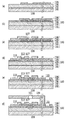
図3に、インクジェットヘッド1についての断面図を示す。図3(a)は、本発明の第1の実施形態に係るインクジェットヘッド用基板100の熱作用部付近について上面から見て模式的に示した断面図である。また、図3(b)は、図3(a)におけるIIIB−IIIB線に沿った模式的な断面図である。
FIG. 3 shows a cross-sectional view of the inkjet head 1. FIG. 3A is a cross-sectional view schematically showing the vicinity of the thermal action portion of the
図3(a)及び図3(b)に示されるように、インクジェットヘッド1では、シリコンによって形成された基体101上に、複数の層が積層されてインクジェットヘッド用基板100が形成される。本実施形態では、基体101上に、熱酸化膜、SiO膜、SiN膜等によって形成される蓄熱層102が配置される。また、蓄熱層102上には、発熱抵抗体層104が配置され、発熱抵抗体層104上には、Al、Al−Si、Al−Cu等の金属材料から形成される配線としての電極配線層105が配置されている。電極配線層105上には、保護層106(第2の保護層)が配置されている。保護層106は、発熱抵抗体層104及び電極配線層105を覆うように、これらの上側に設けられている。保護層106は、SiO膜、SiN膜等によって形成され、絶縁層としても機能する。
As shown in FIGS. 3A and 3B, in the inkjet head 1, a plurality of layers are laminated on a base 101 formed of silicon to form an
保護層106上には、上部保護層107(第1の保護層)が配置されている。上部保護層107は、発熱抵抗体108の発熱に伴う化学的、物理的衝撃から発熱抵抗体108の表面を保護する。本実施形態では、上部保護層107は、イリジウム(Ir)、ルテニウム(Ru)等の白金族、あるいはタンタル(Ta)によって形成されている。また、これらの材料によって形成された上部保護層107は、導電性を有している。インクの吐出が行われる際には、上部保護層107の上部はインクと接触しており、上部保護層107の上部でインクの温度が瞬間的に上昇して発泡し、そこで消泡してキャビテーションの生じる過酷な環境にある。そのため、本実施形態では、耐食性が高く、信頼性の高い材料によって形成された上部保護層107が、発熱抵抗体108に対応する位置に形成される。
An upper protective layer 107 (first protective layer) is disposed on the
電気熱変換素子としての発熱抵抗体108は、電極配線層105が部分的に除去されることによって形成されている。本実施形態では、インク供給口から液室132に向かう方向に沿って、発熱抵抗体層104及び電極配線層105が重ねられて略同じ形状に配置されている。そして、電極配線層105のうちの一部が部分的に除去されることによって、その部分が電極配線層105の存在しないギャップとして形成され、そこでは発熱抵抗体層104のみが配置されている。そのため、発熱抵抗体層104及び電極配線層105が二層に形成されつつ、発熱抵抗体108として機能する部分に対応する部分のみ電極配線層105が除去されている形状となっている。電極配線層105は、不図示の駆動素子回路ないし外部電源端子に接続されており、外部からの電力の供給を受けることができるように構成されている。なお、上記の実施形態では、発熱抵抗体層104上に電極配線層105を配置している構成としたが、本発明はこれに限定されない。電極配線層105を基体101または熱酸化膜102上に形成し、そこで電極配線層105の一部を部分的に除去してギャップを形成して、その電極配線層105の上に発熱抵抗体層104を配置する構成を採用してもよい。
The
一つの液室132の内部に発熱抵抗体108上に対応して形成された上部保護層107は、液室132の内部に配置されている部分から、インク供給口の形成されている部分に向かって延びている。また、その上部保護層107は、液室132の外側で、他の液室から延びた上部保護層107と合流してそれぞれ接続されている。本実施形態では、それぞれの液室132からインク供給口の方へ延びて、それぞれ接続された部分である共通部(共通配線部)110が、吐出口列に沿って形成されている。それぞれの液室132から延びた共通部110は、液室132の外部で一旦合流し、そこから配線(接続配線部)として配置されている。また、共通部110が合流した配線は、外部電極(外部電極部)111と接続されている。なお、共通部110は上部保護層107と同じ層で形成されている。すなわち、上部保護層107は、発熱抵抗体108上にそれぞれ対応して設けられた個別部と、それらを共通に接続する共通部110とを有している。以降、発熱抵抗体108上に対応する個別部のことを上部保護層107とも称する。
The upper
また、それぞれの液室132の内部に配置された上部保護層107には、発熱抵抗体108に対応する部分と、共通部110との間に、薄く形成された薄膜領域(破断部)113が形成されている。ここでは、上部保護層107と薄膜領域113と共通部110とが同じ材料によって形成されている。ここでは特に、上部保護層107と薄膜領域113と共通部110とが、Ir、Ruのいずれか、あるいはIr、Ruのいずれかを含む合金によって形成されている。なお、上述したように、上部保護層107と薄膜領域113と共通部110とは、Taによって形成されても良い。
In addition, in the upper
図4(a)に、薄膜領域113についての模式的な平面図を示す。また、図4(b)に、図4(a)における薄膜領域113のIVB−IVB線に沿う模式的な断面図を示す。上部保護層107の薄膜領域113は、上部保護層107におけるインクと接する領域に形成されている。本実施形態では、全体に亘って略均一の厚さに配置された上部保護層107のうち、一部について、厚みを薄く形成することで、薄膜領域113が形成されている。
FIG. 4A shows a schematic plan view of the
上部保護層107の薄膜領域113の部分については、表面でのキャビテーション等の物理的衝撃や化学的な影響を受けたとしても高寿命を確保することを目標としているため、200〜500nm程度と比較的厚く形成されている。これに対し、薄膜領域113では、10〜100nmと薄く形成されている。
The
(回路構成について)
図5(a)〜(c)に、本実施形態におけるそれぞれの状態のインクジェットヘッド1の回路図について示す。図5(a)に、正常に記録が行われている際のインクジェットヘッド1についての回路図を示す。それぞれの発熱抵抗体108は、電源301、スイッチングトランジスタ114及び選択回路115によって選択されて駆動されている。本実施形態では、電源301は、20〜35Vの電圧である。ここでは、電源301は、24Vの電圧のものが採用されている。このような構成により、所定のタイミングで発熱抵抗体108に電源301からの電力を供給することができ、所定のタイミングで吐出口からインク滴を吐出することができる。
(About circuit configuration)
5A to 5C are circuit diagrams of the ink jet head 1 in each state according to the present embodiment. FIG. 5A shows a circuit diagram of the inkjet head 1 when recording is performed normally. Each
発熱抵抗体108と上部保護層107との間には、絶縁層として機能する保護層106が配置されているので、発熱抵抗体108と上部保護層107とは、電気的に接続されているわけではない。また、上部保護層107は、薄膜領域113を介して共通部110に接続されている。また、共通部110は、外部電極に接続されている。
Since the
図5(b)に、絶縁層として機能する保護層106についての絶縁性の試験を行う際の、インクジェットヘッド1の回路図を示す。保護層106についての絶縁性の試験は、出荷前といったインクジェットヘッド1の内部にインクが存在しない状態で行われる。保護層106の絶縁性を確認するための測定装置302は、発熱抵抗体108に電力を供給するための配線に設けられた電極111aと、共通部110に接続された配線に設けられた電極111bとに接続されるように、配置されている。測定装置302は、プローブピン(針)302a、302bを備えている。これらのプローブピン302a、302bが、電極111a、111bに接続されることで、これらの間に電流が流れている場合には、その電流を検知することができる。電極111a、111bの間に電流が検知されない場合には、保護層106の絶縁性が確実に保たれていることが確認される。また、電極111a、111bの間で電流が流れていることが検知された場合には、保護層106の絶縁性が損なわれており、発熱抵抗体108に供給される電流の一部が上部保護層107に流れていることが検知される。
FIG. 5B is a circuit diagram of the inkjet head 1 when performing an insulation test on the
また、インクジェットヘッド1には、スイッチングトランジスタ114から延びた配線に電極111cが設けられている。電極111aと電極111cにそれぞれプローブピン302a、302bを接続し、これらの間に電流が流れているかどうかを検知することで、発熱抵抗体108やスイッチングトランジスタ114が正常に機能しているかどうかを検知することができる。これらの試験が行われる際には、上部保護層107と、発熱抵抗体108や電極配線105との間に、実際にかかる電圧以上の電圧を印加して流れる電流を測定する。この検査が行われる際には、上部保護層107及び薄膜領域113は、インクと接していないため、電圧を印加しても、インクを介しての上部保護層107における陽極酸化等の電気化学反応は起こらない。そのため、上部保護層107と、発熱抵抗体108、電極配線層105との間のリーク電流の有無に関する電流の測定を確実に行うことができる。
In addition, the inkjet head 1 is provided with an
上部保護層107へ電流が流れることによる上部保護層107の陽極酸化は、インクジェットヘッド1の製造時に、絶縁性を有する保護層106にピンホール等が生じることによって絶縁性が保たれなくなったときに起こることが多い。そのため、保護層106の絶縁性が確保されているかの確認は、製造時に行われることが好ましい。このときの確認のための試験については、上部保護層107が形成され、その後に電気を印加するための外部電極111が形成された後の段階が適している。
The anodic oxidation of the upper
記録が行われる過程で、何らかの理由により、電極配線層105と上部保護層107との間に電流が流れてしまう短絡が生じる可能性がある。電極配線層105と上部保護層107との間で短絡が生じ、電極配線層105を流れる電流の一部が薄膜領域113に向かったときのインクジェットヘッド1における回路について、図5(c)に示す。
In the process of recording, there is a possibility that a short circuit in which a current flows between the
図5(c)の矢印で示されるように、電極配線層105と上部保護層107との間で短絡が生じると、薄膜領域113に向かう方向への電流が生じる。
As indicated by an arrow in FIG. 5C, when a short circuit occurs between the
例えば、発熱抵抗体108が破損したときには、その影響によって保護層106が破断する場合がある。そのとき、発熱抵抗体層104と上部保護層107の一部が溶融し、これらが直接接触して短絡200が生じる可能性がある。このような短絡が生じた場合には、上部保護層107に電圧がかかる可能性がある。そこで、上部保護層107がTaである場合には、上部保護層107がインクとの間で電気化学反応を起こし、そこで陽極酸化が始まる。陽極酸化が進むと、酸化したTaはインクに溶け出すため、上部保護層107の寿命が短くなる。また、上部保護層107がIrやRuである場合には、上部保護層107とインクとの間の電気化学反応により、上部保護層107がインクに溶出するために、上部保護層107の耐久性が低下する。
For example, when the
このとき、共通部110を介して電圧が上部保護層107全体にかかるため、短絡による影響が他の液室の内部にまで及んでしまう可能性がある。従って、陽極酸化やインクとの間の電気化学反応による上部保護層107の耐久性の低下が、インクジェットヘッド1で広範囲に亘って及んでしまい、短絡による影響が拡大してしまう可能性がある。
At this time, since the voltage is applied to the entire upper
本実施形態では、上部保護層107と共通部110との間に薄膜領域113が形成されている。従って、電極配線層105と上部保護層107との間で短絡が生じ、上部保護層107に電流が流れたときには、薄膜領域113にも電気が流れる。このとき、上部保護層107及び薄膜領域113は、インクと接した状態にあり、且つ、上部保護層107は白金族もしくはTaによって形成されている。従って、上述したように、上部保護層107に電流が流れたときには、上部保護層107がTaである場合には、上部保護層107がインクとの間で電気化学反応を起こし、そこで陽極酸化が生じ、上部保護層107がインクに溶出する。また、上部保護層107がIrやRuといった白金族である場合には、上部保護層107とインクとの間で電気化学反応が生じ、上部保護層107がインクに溶出する。液室132の内部にインクが貯留され、発熱抵抗体108に通電されて駆動されるときには、インクの電位は、発熱抵抗体108の駆動電位よりも低い。従って、電極配線層105と上部保護層107との間で短絡が生じたときに上部保護層107へ電気が流れると、上部保護層107とインクとの間で容易に電気化学反応が生じる。
In the present embodiment, a
このように、インクジェットヘッド1にインクが貯留された状態で上部保護層107に電流が流れると、上部保護層107は部分的にインクに溶出する。上部保護層107に電流が流れたときには、薄膜領域113にも電流が流れる。薄膜領域113は、溶出したときに破断され易いように、薄く形成されている。そのため、上部保護層107に電流が流れたときには、比較的容易に薄膜領域113が破断されて、発熱抵抗体108と共通部110との間の電気的な接続が比較的容易に遮断される。このように、薄膜領域113は、そこに電気が流れたときに優先的に破断され、上部保護層107と共通部110との間の電気的な接続を遮断する。
Thus, when a current flows through the upper
また、薄膜領域113は、発熱抵抗体108と、共通部110との間に形成されている。薄膜領域113は、発熱抵抗体108と、共通部110とを接続している部分の幅方向の全体に亘って形成されている。従って、薄膜領域113が溶出したときには、発熱抵抗体108と共通部110との間の電気的な接続が、確実に遮断されるように配置されている。
The
このように、本実施形態では、上部保護層107に電流が流れたときに、インクとの間の電気化学的な反応によって容易に破断されて電気的な接続を遮断する薄膜領域113が形成されている。本実施形態では、薄膜領域113の電気化学反応によって破断されて電気的な接続が遮断されるので、電気的な接続を遮断させるのに大きなエネルギーを必要とせず、比較的簡単に電気的な接続を遮断することができる。そのため、上部保護層107に電流が流れたときには、発熱抵抗体108と、共通部110との間の電気的な接続を確実に遮断することができる。このように、薄膜領域113の電気化学反応によって電気的な接続が遮断されるので、電気的な接続を遮断するヒューズ部としての信頼性を向上させることができる。従って、上部保護層107を流れる電流が他の液室における発泡及び他の吐出口からのインク滴の吐出に影響を与えることを抑えることができる。
As described above, in the present embodiment, the
他の液室へ影響が波及することを抑えることができるので、一つの液室の内部で電気的な短絡が生じて、インク滴の吐出を行うことができなくなったとしても、他の液室については、インク内で正常に発泡させ、インクの吐出を正常に行うことができる。従って、一つの液室の内部で生じる電気的な短絡について、影響を小さく食い止めることができる。そのため、一つの液室の内部で電気的な短絡が生じたとしても、そのことによる記録画像の品質の低下を小さく抑えることができる。また、一つの液室の内部で電気的な短絡が生じたとしても、周辺の液室からのインクの吐出を正常に行うことができるので、周辺の吐出口からのインク滴の吐出によって、短絡の生じた吐出口からのインク滴の吐出について比較的容易にこれを補間することができる。また、一つの液室の内部について、電極配線層105と上部保護層107との間で短絡が生じたとしても、それだけでインクジェットヘッド1の交換をする必要がなくなる。従って、インクジェットヘッド1を長く使用することができ、インクジェットヘッド1の寿命を長くすることができる。これに伴い、インクジェット記録装置1000の運転コストを低く抑えることができる。
Since the influence on other liquid chambers can be suppressed, even if an electrical short circuit occurs within one liquid chamber and ink droplets cannot be discharged, the other liquid chambers Can be normally foamed in the ink, and the ink can be ejected normally. Therefore, the influence of an electrical short circuit that occurs inside one liquid chamber can be reduced. For this reason, even if an electrical short circuit occurs in one liquid chamber, it is possible to suppress a decrease in the quality of a recorded image due to that. In addition, even if an electrical short circuit occurs in one liquid chamber, the ink can be normally discharged from the peripheral liquid chamber, so that the short circuit is caused by the discharge of ink droplets from the peripheral discharge port. This can be interpolated relatively easily for the ejection of ink droplets from the ejection port where the ink has occurred. Further, even if a short circuit occurs between the
仮に、上部保護層107と共通部110との間の部分にポリシリコンの用いられたヒューズ素子が配置される場合には、電流が流れたときに生じる熱によってヒューズ素子内のポリシリコンによる電気的な接続を切断することが必要になる。一般に、ヒューズ素子に使われるポリシリコンは、融点が約1400℃程度である。そのため、ヒューズ素子によって電気的な接続を切断するためには、ヒューズ素子内で1400℃以上の熱が発生するような大きさの電流が流れることが必要になる。このように、ヒューズ素子の電気的な接続を切断するためには、比較的大きなエネルギーが必要となる。一方で、上述したように本実施形態では、薄膜領域113を電気化学反応によってインクに溶出させるため、大きなエネルギーを必要とすることなく短絡が生じた上部保護層107と共通部110との電気接続を遮断することが可能となる。
If a fuse element using polysilicon is disposed in a portion between the upper
(第1実施例)
以下に本発明の第1実施例について説明する。
(First embodiment)
The first embodiment of the present invention will be described below.
(インクジェットヘッドの層構成、及び製造方法)
第1実施に係るインクジェットヘッドの製造工程について説明する。図6(a)〜(f)は、第1実施例に係るインクジェットヘッド用基板100の製造工程について説明するための模式的断面図である。また、図7(a)〜(f)は、インクジェットヘッド用基板100の製造工程における模式的な平面図である。
(Layer configuration of inkjet head and manufacturing method)
The manufacturing process of the inkjet head according to the first embodiment will be described. 6A to 6F are schematic cross-sectional views for explaining the manufacturing process of the
なお、通常、インクジェットヘッド1の製造工程では、Siによって形成された基体101に、駆動回路が予め作り込こまれた状態で、基体101上にそれぞれの層が積層されてインクジェットヘッド1が製造される。発熱抵抗体108を選択的に駆動するためのスイッチングトランジスタ114といった半導体素子等が、駆動回路として基体101に予め作り込まれ、その上に各層が積層されてインクジェットヘッド1が形成される。しかしながら、ここでは簡略化のために、予め配置された駆動回路等については図示されておらず、図6、7では基体101のみが示されている。
Normally, in the manufacturing process of the inkjet head 1, the inkjet head 1 is manufactured by laminating the respective layers on the
まず、基体101上に、熱酸化法、スパッタ法、CVD法などによって、発熱抵抗体層104の下部層としてSiO2の熱酸化膜からなる蓄熱層102を形成する。なお、駆動回路を予め作り込んだ基体に対しては、それら駆動回路の製造プロセス中で蓄熱層を形成可能である。
First, a
次に、蓄熱層102上にTaSiN等の発熱抵抗体層104を、反応スパッタリングにより約50nmの厚さに形成する。また、発熱抵抗体層104上にAl層をスパッタリングにより約300nmの厚さに形成することにより、電極配線層105が形成される。そして、フォトリソグラフィ法を用い、発熱抵抗体層104及び電極配線層105に対して同時にドライエッチングを施す。これにより、発熱抵抗体層104及び電極配線層105以外の部分を除去することで、図7(a)に示される形状の発熱抵抗体層104及び電極配線層105を形成する。なお、本実施形態では、ドライエッチングとしてリアクティブイオンエッチング(RIE)法を用いている。
Next, a
次に、発熱抵抗体108を形成するために、図6(a)及び図7(b)に示されるように、再びフォトリソグラフィ法を用いて、ウエットエッチングによりAlの電極配線層105を部分的に除去し、その部分の発熱抵抗体層104を露出させる。なお、電極配線層105の端部では、保護層106によるカバレッジ性を良好なものとするため、電極配線層105の端部においては、適切なテーパ形状が得られる公知のウエットエッチングの行われることが望ましい。
Next, in order to form the
その後、プラズマCVD法を用いて、図6(b)及び図7(c)に示されるように、保護層106としてSiN膜を約350nmの厚さに形成する。
Thereafter, as shown in FIGS. 6B and 7C, a SiN film is formed to a thickness of about 350 nm as the
次に、上部保護層107として、保護層106上に、スパッタリングにより白金族によって形成された層を約350nmの厚さに形成する。ここでは、上部保護層107は、Irもしくは、Ruによって形成される。次に、図6(c)及び図7(d)に示されるような形状に、フォトリソグラフィ法を用いてドライエッチングにより上部保護層107を部分的に除去する。このとき、発熱部108上の領域に上部保護層107が形成されると共に、上部保護層107と同じ白金属の材料によって、それぞれの液室132の内部に形成された上部保護層107の個別部同士を接続するように、共通部110が形成されている。
Next, as the upper
次に、上部保護層107のうち、薄膜領域113の部分のみを、フォトリソグラフィ法を用いてドライエッチングによって薄く形成する。このとき上部保護層107を全てエッチングするのではなく、薄膜領域113の厚さが約30nmになるように、部分的に上部保護層107が除去されたところでエッチングをストップさせた。これにより、図6(d)及び図7(e)に示すような形状となるように、上部保護層107を形成した。薄膜領域113は、インクジェットヘッド1の内部にインクが収容されたときに直接インクに接するように、液室132の内部やインク流路部に形成されている。
Next, only the
次に、外部電極111を形成するために、図6(e)に示されるように、フォトリソグラフィ法を用いて、ドライエッチングにより保護層106を部分的に除去し、その部分の電極配線層105を部分的に露出させる。
Next, in order to form the
本実施形態の構成では、白金族の材料によって形成された上部保護層107をハーフエッチすることで、図4に示されるように薄膜領域113を薄く形成している。また、発熱抵抗体108に対応する位置では、上部保護層107は、必要とされる耐久性を実現させるために十分な350nmの厚さに形成されている。一方、薄膜領域113では、厚さを30nmとすることで、電極配線層105と上部保護層107との間で短絡200が発生した時に、インクとの電気化学反応により破断するまでインクに溶出し、共通部110との間が絶縁される。
In the configuration of this embodiment, the upper
このとき、ハーフエッチによって薄く形成する部分については、薄膜領域113のみが薄く形成されても良いし、そこから共通部110全体に亘る部分が薄く形成されても良い。しかしながら、共通部110については、保護層106の絶縁性を確認するための試験等を行う際に、共通部110上の部分では、電流が効率的に流れることが必要とされる。従って、本実施例においては、共通部110の厚さは、発熱抵抗体108に対応する位置に形成された上部保護層107と同じ厚さ、ここでは350nmに形成することが好ましい。
At this time, only the
次に、図6(f)、図7(f)に示されるように、インクジェットヘッド用基板100上に、流路形成部材120を配置すると共に、流路形成部材120に吐出口121を形成する。
Next, as shown in FIGS. 6 (f) and 7 (f), the flow
以上の工程を経て、インクジェットヘッド1が製造される。 The inkjet head 1 is manufactured through the above steps.
上記実施形態の構成によれば、電極配線層105と上部保護層107との間で短絡が生じ、上部保護層107に電流が流れたときに、ヒューズを溶断させるのではなく、インクとの電気化学反応により薄膜領域113をインクに溶出させて電気的な接続を遮断する。これにより、短絡によって上部保護層107内に電流が流れる部分を、他の液室に形成された上部保護層107から、電気的に分離させることができる。これにより、ヒューズ素子のように電気的な接続を遮断するのに大きなエネルギーを必要とせず、インクジェットヘッド1の信頼性を向上することができる。さらに、上部保護層107の電気的な接続を遮断するときには、ヒューズ素子のようにインクジェットヘッド1が高温となることを伴わないため、インクジェットヘッド1への熱による影響を低減させることができる。
According to the configuration of the above-described embodiment, when a short circuit occurs between the
なお、インクジェットヘッド1の製造においては、出荷前に、インクジェットヘッド1内にインクを充填させた状態で、外部電極111を介して共通部110に正の電位を印加させることとしても良い。そして、この段階で、全ての液室132内部の薄膜領域113についてインクに溶出させて、電気的な接続を遮断させることとしても良い。出荷の際には、保護層106の絶縁性の試験等については、既に終了していることが多い。その場合、それ以降では、それぞれの液室132内部の発熱抵抗体108に対応する位置から延びた上部保護層107がそれぞれ共通部110で接続されることのメリットがあまりない。従って、その場合には、共通部110に正の電位を印加し、それぞれの液室132内部における薄膜領域113を溶出させ、それぞれの液室132内部の上部保護層107と共通部110との間の電気的な接続を遮断しても良い。すなわち、インクジェットヘッド1の製造工程は、液室132にインクが貯留された状態で、電極(外部電極部)111bに電位を印加し、薄膜領域113を溶出させることで薄膜領域113を破断させる工程を有していても良い。また、電極111bに電位を印加する際の電極111bに印加される電位は、インクの電位よりも高い。これにより、電極111bに電位が印加されたときに、薄膜領域113とインクとの間で容易に電気化学反応が生じる。こうすることにより、それぞれの液室132の間における上部保護層107同士の電気的な接続が遮断され、それぞれの液室132の間で、上部保護層107同士の電気的な接続が切断される。このように、薄膜領域113を溶出させる工程の前に、発熱抵抗体108に配線を介して電流を流したときに、配線と上部保護層107との間に電流が流れる短絡が生じているかどうかの試験を行う工程が行われても良い。このとき、配線に設けられた電源側の電極111a(電源側電極部)と、電極111bとを用いて、短絡が生じているかどうかの試験が行われる。
In manufacturing the inkjet head 1, a positive potential may be applied to the
(第2実施例)
次に、第2実施例のインクジェットヘッドについて説明する。
(Second embodiment)
Next, the ink jet head of the second embodiment will be described.
図8(a)〜(g)に、第2実施例に係るインクジェットヘッドの製造工程について説明するための説明図を示す。図8(a)に、第2実施例のインクジェットヘッドにおける薄膜領域113についての平面図を示し、図8(b)に、図8(a)のVIIIB−VIIIB線に沿う断面図を示す。
FIGS. 8A to 8G are explanatory views for explaining the manufacturing process of the ink jet head according to the second embodiment. FIG. 8A shows a plan view of the
第1実施例におけるインクジェットヘッドでは、上部保護層107が、一つの層によって形成されている。これに対して第2実施例におけるインクジェットヘッドでは、上部保護層107’が、2層に形成されている点で第1実施例におけるインクジェットヘッドと異なる。第2実施例のインクジェットヘッドでは、上部保護層107’のうち、下方に配置された第1の上部保護層107aが300nmに形成され、上方に配置された第2の上部保護層107bが30nmに形成されている。また、第2実施例のインクジェットヘッドでは、第1の上部保護層107aがIrもしくはRuによって形成されており、第2の上部保護層107bがTaによって形成されている。第2実施例では、薄膜領域113は、上部保護層107’を形成する複数の層のうちの1層が共通部110の方へ延びて形成されている。
In the ink jet head in the first embodiment, the upper
図8(c)〜(e)に、第2実施例に係るインクジェットヘッドの製造工程を説明するためのそれぞれの工程におけるインクジェットヘッド用基板の断面図を示す。 8C to 8E are cross-sectional views of the inkjet head substrate in respective steps for explaining the inkjet head manufacturing process according to the second embodiment.
図8(c)に示す段階では、インクジェットヘッド用基板は、第1実施例における図6(b)と同様である。従って、図8(c)の段階までは、製造工程は、第1実施例に示されるインクジェットヘッド用基板の製造工程と同様である。 At the stage shown in FIG. 8C, the inkjet head substrate is the same as FIG. 6B in the first embodiment. Therefore, up to the stage of FIG. 8C, the manufacturing process is the same as the manufacturing process of the ink jet head substrate shown in the first embodiment.
次に、保護層106上に、第1の上部保護層107aが配置される。この工程では、第1の上部保護層107aとして、Ta層が約300nmの厚さに形成されている。第1の上部保護層107aは、スパッタリングによって所定の厚さに形成されている。
Next, the first upper
次に、図8(d)に示されるように、薄膜領域113となる部分の第1の上部保護層107aを部分的に除去する。この工程では、フォトリソグラフィ法を用い、ドライエッチングによって、第1の上部保護層107aのうちの薄膜領域113に対応する部分が除去されている。これにより、第1の上部保護層107aを所定の形状に形成する。
Next, as shown in FIG. 8D, the portion of the first upper
次に、第1の上部保護層107a上に、第2の上部保護層107bが配置される。この工程では、第2の上部保護層107bが、約30nmの厚さに形成される。ここでは、第2の上部保護層107bが、第1の上部保護層107a上を覆うように、第1の上部保護層107a上の全体に亘って形成される。第2実施例では、第2の上部保護層107bは、IrもしくはRu層によって形成されている。第2の上部保護層107bは、スパッタリングによって所定の厚さに形成されている。
Next, the second upper
そして、第2の保護層107bが、図8(e)に示される形状となるように、フォトリソグラフィ法を用いたドライエッチングによって上部保護層107bが部分的に除去される。これによって、上部保護層107bが、所定の形状に形成される。
Then, the upper
この後の外部電極111を形成する工程(図8(f))、流路形成部材120を形成する工程(図8(g))については、第1実施例と同様である。 The subsequent step of forming the external electrode 111 (FIG. 8F) and the step of forming the flow path forming member 120 (FIG. 8G) are the same as in the first embodiment.
以上の製造工程で製造されたインクジェットヘッドでは、薄膜領域113は、第1の上部保護層107aの形成されていない部分に、第2の上部保護層107bのみを配置することによって形成されている。まず、薄膜領域113の位置には第1の上部保護層107aが配置されないように第1の上部保護層107aが所定位置に精度良く配置され、その上から、第2の上部保護層107bが、発熱抵抗体108の周囲の全体に亘って配置される。従って、図8(a)、(b)に示されるように、薄膜領域113には、第2の上部保護層107bのみが配置されることになる。このように、第1の上部保護層107aが部分的に形成されると共に、第2の上部保護層107bが第1の上部保護層107a上の全体に亘って配置されることで形成される。従って、薄膜領域113では、第2の上部保護層107bをスパッタリングによって所定の厚さとなるように形成することができるので、薄膜領域113における膜厚を精度良く形成することができる。
In the inkjet head manufactured by the above manufacturing process, the
(第3実施例)
次に、第3実施例のインクジェットヘッドについて説明する。
(Third embodiment)
Next, an ink jet head according to a third embodiment will be described.
図9(a)〜(g)に、第3実施例に係るインクジェットヘッドの製造工程について説明するための説明図を示す。図9(a)に、第3実施例のインクジェットヘッドにおける薄膜領域113についての平面図を示し、図9(b)に、図9(a)のIXB−IXB線に沿う断面図を示す。第3実施例のインクジェットヘッドでは、上部保護層107’’のうち、下方に配置された第3の上部保護層107cが50nmに形成され、上方に配置された第4の上部保護層107dが250nmに形成されている。第3実施例においても、第2実施例と同様に、薄膜領域113は、上部保護層107’’を形成する複数の層のうちの1層が共通部110の方へ延びて形成されている。また、第3実施例のインクジェットヘッドでは、第3の上部保護層107cがIrもしくはRuによって形成されており、第4の上部保護層107dがTaによって形成されている。
FIGS. 9A to 9G are explanatory views for explaining the manufacturing process of the ink jet head according to the third embodiment. FIG. 9A shows a plan view of the
図9(a)、(b)に示されるように、薄膜領域113では、第4の上部保護層107dが除去されており、第3の上部保護層107cのみが配置されている。図9(c)〜(e)に、第3実施例に係るインクジェットヘッドの製造工程を説明するためのそれぞれの工程におけるインクジェットヘッド用基板の断面図を示す。
As shown in FIGS. 9A and 9B, in the
図9(c)に示す段階では、インクジェットヘッド用基板は、第1実施例における図6(b)と同様である。従って、図9(c)の段階までは、製造工程は、第1実施例及び第2実施例に示されるインクジェットヘッド用基板の製造工程と同様である。 At the stage shown in FIG. 9C, the inkjet head substrate is the same as FIG. 6B in the first embodiment. Therefore, up to the stage of FIG. 9C, the manufacturing process is the same as the manufacturing process of the inkjet head substrate shown in the first and second embodiments.
次に、保護層106上に、第3の上部保護層107cが配置される。この工程では、第3の上部保護層107cが約300nmの厚さに形成されている。本実施例においては、第3の上部保護層107cは、Taの層によって形成されている。また、第3の上部保護層107cは、スパッタリングによって50nmの厚さに形成されている。
Next, the third upper
次に、図9(d)に示されるように、第3の上部保護層107cを所定の形状に形成する。この工程では、フォトリソグラフィ法を用い、ドライエッチングによって、第3の上部保護層107cを所定形状に残し、その他の部分については除去される。
Next, as shown in FIG. 9D, the third upper
次に、第3の上部保護層107c上に、Taの層によって形成された第4の上部保護層107dが配置される。この工程では、第4の上部保護層107dが、約300nmの厚さに形成される。第4の上部保護層107dは、スパッタリングによって約300nmの所定の厚さに形成されている。この工程では、第4の上部保護層107dは、第3の上部保護層107cを覆うように、第3の上部保護層107c上の全体に亘って配置される。
Next, a fourth upper
次に、薄膜領域113の形成される位置で、フォトリソグラフィ法を用いたドライエッチングによって、第4の上部保護層107dが除去される。第3の上部保護層107cに到達するまで第4の上部保護層107dへのエッチングが行われ、その結果、薄膜領域113で第4の上部保護層107dが除去された上部保護層107’’が形成される。これにより、図9(e)に示されるように、薄膜領域113では第3の上部保護層107cのみが配置され、それ以外では第3の上部保護層107c及び第4の上部保護層107dが配置されて積層された上部保護層107’’が形成される。
Next, the fourth upper
この後の外部電極111を形成する工程(図9(f))、流路形成部材120を形成する工程(図9(g))については、第1実施例及び第2実施例と同様である。 The subsequent step of forming the external electrode 111 (FIG. 9 (f)) and the step of forming the flow path forming member 120 (FIG. 9 (g)) are the same as in the first and second embodiments. .
以上の製造工程で製造されたインクジェットヘッドでは、まず、第3の上部保護層107c及び第4の上部保護層107dが配置される。そして、薄膜領域113の形成される位置に対して、第3の上部保護層107cに到達するまでのエッチングが行われ、第4の上部保護層107dが除去されることによって、薄膜領域113が形成されている。従って、薄膜領域113では、第3の上部保護層107cをスパッタリングによって所定の厚さとなるように形成することができるので、薄膜領域113における膜厚を精度良く形成することができる。また、薄膜領域113に対応する位置について、エッチングによって第4の上部保護層107dを除去するので、薄膜領域113の位置精度を向上させることができる。
In the inkjet head manufactured by the above manufacturing process, first, the third upper
また、第3実施例では、第4の上部保護層107dは、上部保護層107cよりも幅方向に広く配置されている。第3の上部保護層107cを形成しているIr及びRuは、保護層106を形成しているSiNと密着性があまり良くないことが知られている。本実施例においては、第3の上部保護層107cのみが保護層106に密着するのでなく、Taによって形成された第4の上部保護層107dも部分的に保護層106と密着している。そのため、第4の上部保護層107dと保護層106とが密着している部分については、これらの間を良好に密着させることができる。
In the third embodiment, the fourth upper
このように、本実施例では、第4の上部保護層107dが保護層106と部分的に接しているので、上部保護層107’’と保護層106との間の密着性に関して、比較的良好な構成である。また、さらに、密着性を向上させるには、第4の上部保護層107dが保護層106との間の接続部以外の場所に、第3の上部保護層107cと保護層106との間に密着層としてTaなどの層を配置しても良い。
Thus, in this example, the fourth upper
(他の実施例)
なお、本明細書において、「記録」とは、文字、図形等有意の情報を形成する場合のみならず、有意無意を問わずに用いられる。また、人間が視覚で知覚し得るように顕在化したものであるか否かを問わず、広く記録媒体上に画像、模様、パターン等を形成する、または記録媒体の加工を行う場合も表すものとする。
(Other examples)
In the present specification, “recording” is used not only for forming significant information such as characters and graphics but also for any case. It also represents the case where images, patterns, patterns, etc. are widely formed on a recording medium, or the recording medium is processed, regardless of whether it is manifested so that it can be perceived by human eyes. And
また、「記録装置」とは、プリンタ、プリンタ複合機、複写機、ファクシミリ装置などのプリント機能を有する装置、ならびにインクジェット技術を用いて物品の製造を行なう製造装置を含む。 The “recording device” includes a device having a printing function such as a printer, a printer multifunction device, a copying machine, and a facsimile device, and a manufacturing device that manufactures an article using an ink jet technique.
また、「記録媒体」とは、一般的な記録装置で用いられる紙のみならず、広く、布、プラスチック・フィルム、金属板、ガラス、セラミックス、木材、皮革等、インクを受容可能なものを表すものとする。 “Recording medium” means not only paper used in general recording apparatuses but also a wide range of materials that can accept ink, such as cloth, plastic film, metal plate, glass, ceramics, wood, leather, etc. Shall.
さらに、「インク」(「液体」と言う場合もある)とは、上記「記録」の定義と同様広く解釈されるべきものである。記録媒体上に付与されることによって、画像、模様、パターン等の形成または記録媒体の加工、或いはインクの処理(例えば記録媒体に付与されるインク中の色剤の凝固または不溶化)に供され得る液体を表すものとする。 Furthermore, “ink” (sometimes referred to as “liquid”) should be interpreted widely as in the definition of “recording”. By being applied on the recording medium, it can be used for formation of images, patterns, patterns, etc., processing of the recording medium, or ink processing (for example, solidification or insolubilization of the colorant in the ink applied to the recording medium). It shall represent a liquid.
106 保護層
107 上部保護層
108 発熱抵抗体
110 共通部
113 薄膜領域
106
Claims (14)
前記基体に配置され、通電されることによりインクを加熱するために発熱する複数の発熱抵抗体と、
前記発熱抵抗体を覆い、電気を通すことが可能な保護層と、を備え、
前記保護層は、前記複数の発熱抵抗体をそれぞれ覆う個別部と、共通部と、を備え、
電気が流れたときにインクと接触する位置に設けられ、インクとの間の電気化学反応によって溶出する材料で構成された接続部によって、前記個別部と前記共通部とが接続されていることを特徴とするインクジェットヘッド用基板。 A substrate;
A plurality of heating resistors disposed on the substrate and generating heat to heat the ink when energized;
It said covering the heating resistor, and a protective layer capable of conducting electricity,
The protective layer includes an individual part that covers each of the plurality of heating resistors, and a common part,
Provided at a position in contact with the ink when electricity flows, the connecting portion being of a material for the electrochemical reaction thus eluting between the ink, the said individual portion and the common portion is connected An ink jet head substrate characterized by the above.
前記接続部は、前記保護層を形成する前記複数の層のうちの1層によって形成されていることを特徴とする請求項1から5のいずれか1項に記載のインクジェットヘッド用基板。 The protective layer is formed by laminating a plurality of layers,
Said connecting portion, said plurality of substrates for ink jet head according to any one of claims 1 to 5, it is characterized in being formed by one of the layers forming the protective layer.
前記接続部は、前記個別部よりも前記延在する方向に直交する方向の長さが短いことを特徴とする請求項1から7のいずれか1項に記載のインクジェットヘッド用基板。 8. The inkjet head substrate according to claim 1, wherein the connection portion has a shorter length in a direction orthogonal to the extending direction than the individual portion.
前記インクジェットヘッド用基板の前記保護層が配置された側の面に取り付けられ、吐出口の形成された流路形成部材と、
前記流路形成部材と前記インクジェットヘッド用基板とで画成され、内部にインクを貯留させることが可能な複数の液室であって、前記発熱抵抗体が前記液室ごとに配置された前記複数の液室と、
前記液室に貯留されたインクを前記発熱抵抗体によって加熱して前記吐出口からインク滴を吐出するインクジェットヘッドであって、
前記保護層は、前記複数の発熱抵抗体をそれぞれ覆い、前記液室の内部に露出して設けられた個別部と、共通部と、を備え、
前記液室の内部にインクが貯留されたときにはインクと接する位置に形成され、インクとの間の電気化学反応によって溶出する材料で構成された接続部によって、前記個別部と前記共通部とが接続されていることを特徴とするインクジェットヘッド。 A substrate, a plurality of heating resistors that are disposed on the substrate and generate heat to heat ink when energized, and a protective layer that covers the heating resistor and allows electricity to pass therethrough. An inkjet head substrate;
A flow path forming member attached to the surface of the inkjet head substrate on which the protective layer is disposed and having a discharge port formed thereon;
A plurality of liquid chambers defined by the flow path forming member and the inkjet head substrate and capable of storing ink therein, wherein the plurality of heating resistors are arranged for each liquid chamber. Liquid chamber,
An ink jet head that discharges ink droplets from the discharge port by heating ink stored in the liquid chamber with the heating resistor,
The protective layer covers the plurality of heating resistors, respectively, comprising an individual portion provided exposed to the interior of the liquid chamber, and a common portion,
When the ink is stored inside the liquid chamber is formed in a position in contact with the ink, the connecting portion being of a material for the electrochemical reaction thus eluting between the ink, and a separate processing unit and the common unit An inkjet head characterized by being connected.
前記インクジェットヘッド用基板の前記保護層が配置された側の面に取り付けられ、吐出口の形成された流路形成部材と、
前記流路形成部材と前記インクジェットヘッド用基板とで画成され、内部にインクを貯留させることが可能な複数の液室であって、前記発熱抵抗体が前記液室ごとに配置された前記複数の液室と、を有するインクジェットヘッドであって、
前記保護層は、前記複数の発熱抵抗体をそれぞれ覆い、前記液室の内部に露出して設けられた個別部と、共通部と、を備え、
前記インクジェットヘッド用基板は、前記共通部に電気的に接続された外部電極部を備えた、インクジェットヘッドの製造方法であって、
前記液室にインクが貯留された状態で前記外部電極部に電位を印加し、前記個別部と前記共通部とを接続する接続部とインクとの間で電気化学反応を生じさせて前記接続部をインクに溶出させて破断させることで、前記個別部と前記共通部との間の電気的な接続を遮断する工程を有することを特徴とするインクジェットヘッドの製造方法。 A substrate, a plurality of heating resistors that are disposed on the substrate and generate heat to heat ink when energized, and a protective layer that covers the heating resistor and allows electricity to pass therethrough. An inkjet head substrate;
A flow path forming member attached to the surface of the inkjet head substrate on which the protective layer is disposed and having a discharge port formed thereon;
A plurality of liquid chambers defined by the flow path forming member and the inkjet head substrate and capable of storing ink therein, wherein the plurality of heating resistors are arranged for each liquid chamber. An ink jet head comprising:
The protective layer covers the plurality of heating resistors, respectively, comprising an individual portion provided exposed to the interior of the liquid chamber, and a common portion,
The ink jet head circuit board, the common portion with an external electrode portion that is electrically connected to a manufacturing method of the ink jet head,
In the state where ink is stored in the liquid chamber, an electric potential is applied to the external electrode portion, and an electrochemical reaction is caused between the connection portion connecting the individual portion and the common portion and the ink, and the connection portion. Ink jet head manufacturing method characterized by having a step of cutting off electrical connection between the individual part and the common part by eluting the ink into ink and causing it to break.
Priority Applications (3)
| Application Number | Priority Date | Filing Date | Title |
|---|---|---|---|
| JP2012285440A JP6039411B2 (en) | 2012-12-27 | 2012-12-27 | Inkjet head substrate, inkjet head, and inkjet head manufacturing method |
| US14/138,295 US9061489B2 (en) | 2012-12-27 | 2013-12-23 | Substrate for inkjet head and inkjet head having protection layer including individual sections corresponding to heating resistors |
| CN201310741027.1A CN103895349B (en) | 2012-12-27 | 2013-12-27 | The substrate of ink gun and ink gun |
Applications Claiming Priority (1)
| Application Number | Priority Date | Filing Date | Title |
|---|---|---|---|
| JP2012285440A JP6039411B2 (en) | 2012-12-27 | 2012-12-27 | Inkjet head substrate, inkjet head, and inkjet head manufacturing method |
Publications (3)
| Publication Number | Publication Date |
|---|---|
| JP2014124921A JP2014124921A (en) | 2014-07-07 |
| JP2014124921A5 JP2014124921A5 (en) | 2016-02-18 |
| JP6039411B2 true JP6039411B2 (en) | 2016-12-07 |
Family
ID=50987068
Family Applications (1)
| Application Number | Title | Priority Date | Filing Date |
|---|---|---|---|
| JP2012285440A Expired - Fee Related JP6039411B2 (en) | 2012-12-27 | 2012-12-27 | Inkjet head substrate, inkjet head, and inkjet head manufacturing method |
Country Status (3)
| Country | Link |
|---|---|
| US (1) | US9061489B2 (en) |
| JP (1) | JP6039411B2 (en) |
| CN (1) | CN103895349B (en) |
Families Citing this family (11)
| Publication number | Priority date | Publication date | Assignee | Title |
|---|---|---|---|---|
| JP6566709B2 (en) | 2015-05-07 | 2019-08-28 | キヤノン株式会社 | Inkjet recording head substrate |
| JP6504938B2 (en) * | 2015-06-25 | 2019-04-24 | キヤノン株式会社 | Substrate for liquid discharge head and liquid discharge head |
| US10272671B2 (en) | 2015-10-08 | 2019-04-30 | Hewlett-Packard Development Company, L.P. | Isolating failed resistors |
| JP2018176697A (en) * | 2017-04-21 | 2018-11-15 | キヤノン株式会社 | Method of disconnecting fuse part of liquid discharge head, and liquid discharge device |
| JP7071067B2 (en) * | 2017-06-21 | 2022-05-18 | キヤノン株式会社 | A method for manufacturing a substrate for a liquid discharge head, a liquid discharge head, and a substrate for a liquid discharge head. |
| JP2019069533A (en) * | 2017-10-06 | 2019-05-09 | キヤノン株式会社 | Substrate for liquid discharge head, liquid discharge head, and cutting method for fuse part in the substrate |
| JP7183049B2 (en) | 2018-02-22 | 2022-12-05 | キヤノン株式会社 | LIQUID EJECTION HEAD SUBSTRATE AND LIQUID EJECTION HEAD |
| JP7159060B2 (en) | 2018-02-22 | 2022-10-24 | キヤノン株式会社 | Substrate for liquid ejection head, liquid ejection head, method for manufacturing liquid ejection head substrate |
| JP7286349B2 (en) * | 2018-04-27 | 2023-06-05 | キヤノン株式会社 | LIQUID EJECTION HEAD SUBSTRATE, LIQUID EJECTION HEAD SUBSTRATE MANUFACTURING METHOD, AND LIQUID EJECTION HEAD |
| JP7134733B2 (en) | 2018-06-25 | 2022-09-12 | キヤノン株式会社 | PRINTING ELEMENT SUBSTRATE, LIQUID EJECTION HEAD, AND LIQUID EJECTION APPARATUS |
| JP2023049392A (en) | 2021-09-29 | 2023-04-10 | キヤノン株式会社 | Substrate for liquid discharge head, liquid discharge head, and manufacturing method for substrate for liquid discharge head |
Family Cites Families (24)
| Publication number | Priority date | Publication date | Assignee | Title |
|---|---|---|---|---|
| JPH062416B2 (en) * | 1984-01-30 | 1994-01-12 | キヤノン株式会社 | Liquid jet recording head manufacturing method |
| ATE191884T1 (en) | 1993-07-29 | 2000-05-15 | Canon Kk | INKJET PRINTHEAD, INKJET HEAD CARTRIDGE AND PRINTING DEVICE |
| JP2984914B2 (en) * | 1996-09-05 | 1999-11-29 | 釜屋電機株式会社 | Chip type fuse resistor and its electrode structure |
| US6512284B2 (en) | 1999-04-27 | 2003-01-28 | Hewlett-Packard Company | Thinfilm fuse/antifuse device and use of same in printhead |
| US6361150B1 (en) | 1999-08-30 | 2002-03-26 | Hewlett-Packard Company | Electrostatic discharge protection of electrically-inactive components in a thermal ink jet printing system |
| JP3576888B2 (en) | 1999-10-04 | 2004-10-13 | キヤノン株式会社 | Substrate for inkjet head, inkjet head, and inkjet apparatus |
| JP3710364B2 (en) | 2000-07-31 | 2005-10-26 | キヤノン株式会社 | Inkjet head |
| JP3812485B2 (en) | 2002-04-10 | 2006-08-23 | ソニー株式会社 | Liquid ejection apparatus and printer |
| CN100493912C (en) | 2002-12-27 | 2009-06-03 | 佳能株式会社 | Substrate for ink jet head, ink jet head utilizing the same and producing method therefor |
| EP1547777B1 (en) | 2003-12-26 | 2011-06-08 | Canon Kabushiki Kaisha | Ink jet head, method of driving the ink jet head, and ink jet recording apparatus |
| JP4208793B2 (en) | 2004-08-16 | 2009-01-14 | キヤノン株式会社 | Inkjet head substrate, method for producing the substrate, and inkjet head using the substrate |
| JP4208794B2 (en) | 2004-08-16 | 2009-01-14 | キヤノン株式会社 | Inkjet head substrate, method for producing the substrate, and inkjet head using the substrate |
| JP4646602B2 (en) | 2004-11-09 | 2011-03-09 | キヤノン株式会社 | Manufacturing method of substrate for ink jet recording head |
| JP4926669B2 (en) | 2005-12-09 | 2012-05-09 | キヤノン株式会社 | Inkjet head cleaning method, inkjet head, and inkjet recording apparatus |
| JP4847360B2 (en) | 2006-02-02 | 2011-12-28 | キヤノン株式会社 | Liquid discharge head substrate, liquid discharge head using the substrate, and manufacturing method thereof |
| JP2007230127A (en) * | 2006-03-02 | 2007-09-13 | Canon Inc | Manufacturing method of substrate for inkjet recording head |
| JP2008149687A (en) | 2006-12-20 | 2008-07-03 | Canon Inc | Substrate for ink-jet recording head and ink-jet recording head using substrate |
| JP5147282B2 (en) | 2007-05-02 | 2013-02-20 | キヤノン株式会社 | Inkjet recording substrate, recording head including the substrate, and recording apparatus |
| JP4963679B2 (en) | 2007-05-29 | 2012-06-27 | キヤノン株式会社 | SUBSTRATE FOR LIQUID DISCHARGE HEAD, MANUFACTURING METHOD THEREOF, AND LIQUID DISCHARGE HEAD USING THE SUBSTRATE |
| US8075102B2 (en) | 2008-06-19 | 2011-12-13 | Canon Kabushiki Kaisha | Substrate for ink jet head and ink jet head |
| JP5393275B2 (en) * | 2008-06-24 | 2014-01-22 | キヤノン株式会社 | Liquid discharge head |
| JP5328607B2 (en) | 2008-11-17 | 2013-10-30 | キヤノン株式会社 | Substrate for liquid discharge head, liquid discharge head having the substrate, cleaning method for the head, and liquid discharge apparatus using the head |
| JP2011213049A (en) * | 2010-04-01 | 2011-10-27 | Canon Inc | Liquid discharge head and driving method of the same |
| JP5106601B2 (en) | 2010-08-26 | 2012-12-26 | キヤノン株式会社 | Method for manufacturing liquid discharge head substrate, method for manufacturing liquid discharge head, and method for inspecting liquid discharge head substrate |
-
2012
- 2012-12-27 JP JP2012285440A patent/JP6039411B2/en not_active Expired - Fee Related
-
2013
- 2013-12-23 US US14/138,295 patent/US9061489B2/en not_active Expired - Fee Related
- 2013-12-27 CN CN201310741027.1A patent/CN103895349B/en not_active Expired - Fee Related
Also Published As
| Publication number | Publication date |
|---|---|
| US9061489B2 (en) | 2015-06-23 |
| JP2014124921A (en) | 2014-07-07 |
| US20140184700A1 (en) | 2014-07-03 |
| CN103895349B (en) | 2016-01-20 |
| CN103895349A (en) | 2014-07-02 |
Similar Documents
| Publication | Publication Date | Title |
|---|---|---|
| JP6039411B2 (en) | Inkjet head substrate, inkjet head, and inkjet head manufacturing method | |
| JP6150519B2 (en) | INKJET RECORDING HEAD SUBSTRATE, INKJET RECORDING HEAD, INKJET RECORDING HEAD MANUFACTURING METHOD, INKJET RECORDING DEVICE, AND INKJET RECORDING HEAD SUBSTRATE | |
| JP6143455B2 (en) | Inkjet head substrate, inkjet head, and inkjet recording apparatus | |
| JP6143454B2 (en) | Inkjet head substrate, inkjet head, and inkjet recording apparatus | |
| US9096059B2 (en) | Substrate for inkjet head, inkjet head, and inkjet printing apparatus | |
| JP5627307B2 (en) | Substrate for liquid discharge head and liquid discharge head | |
| US20120047737A1 (en) | Method for manufacturing substrate for liquid ejection head and method for manufacturing liquid ejection head | |
| JP2015223709A (en) | Liquid discharge head | |
| JP5677109B2 (en) | Inkjet recording head substrate, inkjet recording head, and recording apparatus | |
| JP6497902B2 (en) | Recording head substrate, recording head, and recording apparatus | |
| US20150070438A1 (en) | Liquid ejection head and liquid ejection apparatus | |
| US10994532B2 (en) | Liquid discharge apparatus and control method thereof | |
| JP2018176697A (en) | Method of disconnecting fuse part of liquid discharge head, and liquid discharge device | |
| JP6552692B2 (en) | Element substrate, liquid discharge head, and recording apparatus | |
| US11577508B2 (en) | Element substrate, liquid discharge head, and printing apparatus | |
| JP7186540B2 (en) | LIQUID EJECTION HEAD SUBSTRATE, LIQUID EJECTION HEAD, AND LIQUID EJECTION APPARATUS | |
| JP7071067B2 (en) | A method for manufacturing a substrate for a liquid discharge head, a liquid discharge head, and a substrate for a liquid discharge head. | |
| US10421272B2 (en) | Control method of liquid ejection head and liquid ejection apparatus | |
| US20210370669A1 (en) | Liquid discharge head and liquid discharge device | |
| US8104873B2 (en) | Recording head | |
| US9259926B2 (en) | Liquid ejection apparatus and liquid ejection head | |
| JP5317671B2 (en) | Substrate for liquid discharge head, liquid discharge head, and liquid discharge apparatus |
Legal Events
| Date | Code | Title | Description |
|---|---|---|---|
| A521 | Request for written amendment filed |
Free format text: JAPANESE INTERMEDIATE CODE: A523 Effective date: 20151222 |
|
| A621 | Written request for application examination |
Free format text: JAPANESE INTERMEDIATE CODE: A621 Effective date: 20151222 |
|
| TRDD | Decision of grant or rejection written | ||
| A977 | Report on retrieval |
Free format text: JAPANESE INTERMEDIATE CODE: A971007 Effective date: 20160930 |
|
| A01 | Written decision to grant a patent or to grant a registration (utility model) |
Free format text: JAPANESE INTERMEDIATE CODE: A01 Effective date: 20161004 |
|
| A61 | First payment of annual fees (during grant procedure) |
Free format text: JAPANESE INTERMEDIATE CODE: A61 Effective date: 20161104 |
|
| R151 | Written notification of patent or utility model registration |
Ref document number: 6039411 Country of ref document: JP Free format text: JAPANESE INTERMEDIATE CODE: R151 |
|
| LAPS | Cancellation because of no payment of annual fees |