JP4646602B2 - Manufacturing method of substrate for ink jet recording head - Google Patents
Manufacturing method of substrate for ink jet recording head Download PDFInfo
- Publication number
- JP4646602B2 JP4646602B2 JP2004325534A JP2004325534A JP4646602B2 JP 4646602 B2 JP4646602 B2 JP 4646602B2 JP 2004325534 A JP2004325534 A JP 2004325534A JP 2004325534 A JP2004325534 A JP 2004325534A JP 4646602 B2 JP4646602 B2 JP 4646602B2
- Authority
- JP
- Japan
- Prior art keywords
- layer
- substrate
- protective
- material layer
- film
- Prior art date
- Legal status (The legal status is an assumption and is not a legal conclusion. Google has not performed a legal analysis and makes no representation as to the accuracy of the status listed.)
- Expired - Fee Related
Links
- 239000000758 substrate Substances 0.000 title claims description 99
- 238000004519 manufacturing process Methods 0.000 title claims description 36
- 239000010410 layer Substances 0.000 claims description 121
- 239000011241 protective layer Substances 0.000 claims description 87
- 238000010438 heat treatment Methods 0.000 claims description 75
- 239000000463 material Substances 0.000 claims description 52
- 238000000034 method Methods 0.000 claims description 36
- 230000001681 protective effect Effects 0.000 claims description 30
- 238000005530 etching Methods 0.000 claims description 25
- 229910004298 SiO 2 Inorganic materials 0.000 claims description 16
- 238000004544 sputter deposition Methods 0.000 claims description 13
- 239000000203 mixture Substances 0.000 claims description 5
- 239000011810 insulating material Substances 0.000 claims description 4
- 238000005268 plasma chemical vapour deposition Methods 0.000 claims description 4
- 230000004044 response Effects 0.000 claims description 3
- 230000008859 change Effects 0.000 claims description 2
- 239000010408 film Substances 0.000 description 93
- 239000007789 gas Substances 0.000 description 29
- 238000000059 patterning Methods 0.000 description 17
- 230000008569 process Effects 0.000 description 12
- 238000005187 foaming Methods 0.000 description 10
- 230000015572 biosynthetic process Effects 0.000 description 9
- 239000000243 solution Substances 0.000 description 8
- 230000007423 decrease Effects 0.000 description 7
- 238000000206 photolithography Methods 0.000 description 7
- 229910004200 TaSiN Inorganic materials 0.000 description 6
- WGTYBPLFGIVFAS-UHFFFAOYSA-M tetramethylammonium hydroxide Chemical compound [OH-].C[N+](C)(C)C WGTYBPLFGIVFAS-UHFFFAOYSA-M 0.000 description 6
- 238000011156 evaluation Methods 0.000 description 5
- 238000005338 heat storage Methods 0.000 description 5
- 239000011229 interlayer Substances 0.000 description 5
- 238000004528 spin coating Methods 0.000 description 5
- IJGRMHOSHXDMSA-UHFFFAOYSA-N Atomic nitrogen Chemical compound N#N IJGRMHOSHXDMSA-UHFFFAOYSA-N 0.000 description 4
- KRHYYFGTRYWZRS-UHFFFAOYSA-N Fluorane Chemical compound F KRHYYFGTRYWZRS-UHFFFAOYSA-N 0.000 description 4
- 230000009471 action Effects 0.000 description 4
- 239000003795 chemical substances by application Substances 0.000 description 4
- 238000007599 discharging Methods 0.000 description 4
- 238000001312 dry etching Methods 0.000 description 4
- 239000007788 liquid Substances 0.000 description 4
- 238000001039 wet etching Methods 0.000 description 4
- 238000011161 development Methods 0.000 description 3
- 230000000694 effects Effects 0.000 description 3
- 238000009751 slip forming Methods 0.000 description 3
- XKRFYHLGVUSROY-UHFFFAOYSA-N Argon Chemical compound [Ar] XKRFYHLGVUSROY-UHFFFAOYSA-N 0.000 description 2
- 239000003513 alkali Substances 0.000 description 2
- 239000000956 alloy Substances 0.000 description 2
- 229910052799 carbon Inorganic materials 0.000 description 2
- 150000001875 compounds Chemical class 0.000 description 2
- 239000013078 crystal Substances 0.000 description 2
- 238000000151 deposition Methods 0.000 description 2
- 230000008021 deposition Effects 0.000 description 2
- 229910001873 dinitrogen Inorganic materials 0.000 description 2
- 238000010828 elution Methods 0.000 description 2
- 238000001755 magnetron sputter deposition Methods 0.000 description 2
- 239000002184 metal Substances 0.000 description 2
- 229910052751 metal Inorganic materials 0.000 description 2
- 229910052757 nitrogen Inorganic materials 0.000 description 2
- 230000003647 oxidation Effects 0.000 description 2
- 238000007254 oxidation reaction Methods 0.000 description 2
- 229910052760 oxygen Inorganic materials 0.000 description 2
- 238000007639 printing Methods 0.000 description 2
- 238000012545 processing Methods 0.000 description 2
- 238000005546 reactive sputtering Methods 0.000 description 2
- 230000002940 repellent Effects 0.000 description 2
- 239000005871 repellent Substances 0.000 description 2
- 229910052710 silicon Inorganic materials 0.000 description 2
- 229910052715 tantalum Inorganic materials 0.000 description 2
- 238000012360 testing method Methods 0.000 description 2
- XLYOFNOQVPJJNP-UHFFFAOYSA-N water Substances O XLYOFNOQVPJJNP-UHFFFAOYSA-N 0.000 description 2
- 239000004925 Acrylic resin Substances 0.000 description 1
- 229920000178 Acrylic resin Polymers 0.000 description 1
- 229910018125 Al-Si Inorganic materials 0.000 description 1
- 229910018182 Al—Cu Inorganic materials 0.000 description 1
- 229910018520 Al—Si Inorganic materials 0.000 description 1
- OKTJSMMVPCPJKN-UHFFFAOYSA-N Carbon Chemical compound [C] OKTJSMMVPCPJKN-UHFFFAOYSA-N 0.000 description 1
- MYMOFIZGZYHOMD-UHFFFAOYSA-N Dioxygen Chemical compound O=O MYMOFIZGZYHOMD-UHFFFAOYSA-N 0.000 description 1
- 229910004490 TaAl Inorganic materials 0.000 description 1
- 239000012670 alkaline solution Substances 0.000 description 1
- 229910045601 alloy Inorganic materials 0.000 description 1
- 229910052782 aluminium Inorganic materials 0.000 description 1
- 229910052786 argon Inorganic materials 0.000 description 1
- QVGXLLKOCUKJST-UHFFFAOYSA-N atomic oxygen Chemical compound [O] QVGXLLKOCUKJST-UHFFFAOYSA-N 0.000 description 1
- 150000001768 cations Chemical class 0.000 description 1
- 239000000919 ceramic Substances 0.000 description 1
- 229910052804 chromium Inorganic materials 0.000 description 1
- 239000003086 colorant Substances 0.000 description 1
- 238000004891 communication Methods 0.000 description 1
- 230000007797 corrosion Effects 0.000 description 1
- 238000005260 corrosion Methods 0.000 description 1
- 230000003247 decreasing effect Effects 0.000 description 1
- 238000001514 detection method Methods 0.000 description 1
- 230000006866 deterioration Effects 0.000 description 1
- 238000010586 diagram Methods 0.000 description 1
- 229910001882 dioxygen Inorganic materials 0.000 description 1
- 230000009977 dual effect Effects 0.000 description 1
- 239000012777 electrically insulating material Substances 0.000 description 1
- 239000003822 epoxy resin Substances 0.000 description 1
- 239000004744 fabric Substances 0.000 description 1
- 239000000835 fiber Substances 0.000 description 1
- 239000006260 foam Substances 0.000 description 1
- 238000012812 general test Methods 0.000 description 1
- 239000011521 glass Substances 0.000 description 1
- 229910052735 hafnium Inorganic materials 0.000 description 1
- 238000007654 immersion Methods 0.000 description 1
- 238000007641 inkjet printing Methods 0.000 description 1
- 230000009191 jumping Effects 0.000 description 1
- 238000010030 laminating Methods 0.000 description 1
- 238000003475 lamination Methods 0.000 description 1
- 239000010985 leather Substances 0.000 description 1
- 239000012528 membrane Substances 0.000 description 1
- 229910052750 molybdenum Inorganic materials 0.000 description 1
- 239000001301 oxygen Substances 0.000 description 1
- 239000002245 particle Substances 0.000 description 1
- 230000000149 penetrating effect Effects 0.000 description 1
- 230000002093 peripheral effect Effects 0.000 description 1
- 229920002120 photoresistant polymer Polymers 0.000 description 1
- 239000004033 plastic Substances 0.000 description 1
- 229910021420 polycrystalline silicon Inorganic materials 0.000 description 1
- 229920000647 polyepoxide Polymers 0.000 description 1
- 238000011084 recovery Methods 0.000 description 1
- 230000009467 reduction Effects 0.000 description 1
- 239000011347 resin Substances 0.000 description 1
- 229920005989 resin Polymers 0.000 description 1
- 239000004065 semiconductor Substances 0.000 description 1
- 238000004904 shortening Methods 0.000 description 1
- 238000003860 storage Methods 0.000 description 1
- 239000000126 substance Substances 0.000 description 1
- 239000010409 thin film Substances 0.000 description 1
- 229910052719 titanium Inorganic materials 0.000 description 1
- 238000012546 transfer Methods 0.000 description 1
- 238000011144 upstream manufacturing Methods 0.000 description 1
- 239000002023 wood Substances 0.000 description 1
- 229910052726 zirconium Inorganic materials 0.000 description 1
Images


Classifications
-
- B—PERFORMING OPERATIONS; TRANSPORTING
- B41—PRINTING; LINING MACHINES; TYPEWRITERS; STAMPS
- B41J—TYPEWRITERS; SELECTIVE PRINTING MECHANISMS, i.e. MECHANISMS PRINTING OTHERWISE THAN FROM A FORME; CORRECTION OF TYPOGRAPHICAL ERRORS
- B41J2/00—Typewriters or selective printing mechanisms characterised by the printing or marking process for which they are designed
- B41J2/005—Typewriters or selective printing mechanisms characterised by the printing or marking process for which they are designed characterised by bringing liquid or particles selectively into contact with a printing material
- B41J2/01—Ink jet
- B41J2/135—Nozzles
- B41J2/16—Production of nozzles
- B41J2/1601—Production of bubble jet print heads
- B41J2/1603—Production of bubble jet print heads of the front shooter type
-
- B—PERFORMING OPERATIONS; TRANSPORTING
- B41—PRINTING; LINING MACHINES; TYPEWRITERS; STAMPS
- B41J—TYPEWRITERS; SELECTIVE PRINTING MECHANISMS, i.e. MECHANISMS PRINTING OTHERWISE THAN FROM A FORME; CORRECTION OF TYPOGRAPHICAL ERRORS
- B41J2/00—Typewriters or selective printing mechanisms characterised by the printing or marking process for which they are designed
- B41J2/005—Typewriters or selective printing mechanisms characterised by the printing or marking process for which they are designed characterised by bringing liquid or particles selectively into contact with a printing material
- B41J2/01—Ink jet
- B41J2/135—Nozzles
- B41J2/14—Structure thereof only for on-demand ink jet heads
- B41J2/14016—Structure of bubble jet print heads
- B41J2/14088—Structure of heating means
- B41J2/14112—Resistive element
- B41J2/14129—Layer structure
-
- B—PERFORMING OPERATIONS; TRANSPORTING
- B41—PRINTING; LINING MACHINES; TYPEWRITERS; STAMPS
- B41J—TYPEWRITERS; SELECTIVE PRINTING MECHANISMS, i.e. MECHANISMS PRINTING OTHERWISE THAN FROM A FORME; CORRECTION OF TYPOGRAPHICAL ERRORS
- B41J2/00—Typewriters or selective printing mechanisms characterised by the printing or marking process for which they are designed
- B41J2/005—Typewriters or selective printing mechanisms characterised by the printing or marking process for which they are designed characterised by bringing liquid or particles selectively into contact with a printing material
- B41J2/01—Ink jet
- B41J2/135—Nozzles
- B41J2/16—Production of nozzles
- B41J2/1621—Manufacturing processes
- B41J2/1626—Manufacturing processes etching
- B41J2/1628—Manufacturing processes etching dry etching
-
- B—PERFORMING OPERATIONS; TRANSPORTING
- B41—PRINTING; LINING MACHINES; TYPEWRITERS; STAMPS
- B41J—TYPEWRITERS; SELECTIVE PRINTING MECHANISMS, i.e. MECHANISMS PRINTING OTHERWISE THAN FROM A FORME; CORRECTION OF TYPOGRAPHICAL ERRORS
- B41J2/00—Typewriters or selective printing mechanisms characterised by the printing or marking process for which they are designed
- B41J2/005—Typewriters or selective printing mechanisms characterised by the printing or marking process for which they are designed characterised by bringing liquid or particles selectively into contact with a printing material
- B41J2/01—Ink jet
- B41J2/135—Nozzles
- B41J2/16—Production of nozzles
- B41J2/1621—Manufacturing processes
- B41J2/1626—Manufacturing processes etching
- B41J2/1629—Manufacturing processes etching wet etching
-
- B—PERFORMING OPERATIONS; TRANSPORTING
- B41—PRINTING; LINING MACHINES; TYPEWRITERS; STAMPS
- B41J—TYPEWRITERS; SELECTIVE PRINTING MECHANISMS, i.e. MECHANISMS PRINTING OTHERWISE THAN FROM A FORME; CORRECTION OF TYPOGRAPHICAL ERRORS
- B41J2/00—Typewriters or selective printing mechanisms characterised by the printing or marking process for which they are designed
- B41J2/005—Typewriters or selective printing mechanisms characterised by the printing or marking process for which they are designed characterised by bringing liquid or particles selectively into contact with a printing material
- B41J2/01—Ink jet
- B41J2/135—Nozzles
- B41J2/16—Production of nozzles
- B41J2/1621—Manufacturing processes
- B41J2/1631—Manufacturing processes photolithography
-
- B—PERFORMING OPERATIONS; TRANSPORTING
- B41—PRINTING; LINING MACHINES; TYPEWRITERS; STAMPS
- B41J—TYPEWRITERS; SELECTIVE PRINTING MECHANISMS, i.e. MECHANISMS PRINTING OTHERWISE THAN FROM A FORME; CORRECTION OF TYPOGRAPHICAL ERRORS
- B41J2/00—Typewriters or selective printing mechanisms characterised by the printing or marking process for which they are designed
- B41J2/005—Typewriters or selective printing mechanisms characterised by the printing or marking process for which they are designed characterised by bringing liquid or particles selectively into contact with a printing material
- B41J2/01—Ink jet
- B41J2/135—Nozzles
- B41J2/16—Production of nozzles
- B41J2/1621—Manufacturing processes
- B41J2/164—Manufacturing processes thin film formation
- B41J2/1642—Manufacturing processes thin film formation thin film formation by CVD [chemical vapor deposition]
-
- B—PERFORMING OPERATIONS; TRANSPORTING
- B41—PRINTING; LINING MACHINES; TYPEWRITERS; STAMPS
- B41J—TYPEWRITERS; SELECTIVE PRINTING MECHANISMS, i.e. MECHANISMS PRINTING OTHERWISE THAN FROM A FORME; CORRECTION OF TYPOGRAPHICAL ERRORS
- B41J2/00—Typewriters or selective printing mechanisms characterised by the printing or marking process for which they are designed
- B41J2/005—Typewriters or selective printing mechanisms characterised by the printing or marking process for which they are designed characterised by bringing liquid or particles selectively into contact with a printing material
- B41J2/01—Ink jet
- B41J2/135—Nozzles
- B41J2/16—Production of nozzles
- B41J2/1621—Manufacturing processes
- B41J2/164—Manufacturing processes thin film formation
- B41J2/1645—Manufacturing processes thin film formation thin film formation by spincoating
-
- B—PERFORMING OPERATIONS; TRANSPORTING
- B41—PRINTING; LINING MACHINES; TYPEWRITERS; STAMPS
- B41J—TYPEWRITERS; SELECTIVE PRINTING MECHANISMS, i.e. MECHANISMS PRINTING OTHERWISE THAN FROM A FORME; CORRECTION OF TYPOGRAPHICAL ERRORS
- B41J2/00—Typewriters or selective printing mechanisms characterised by the printing or marking process for which they are designed
- B41J2/005—Typewriters or selective printing mechanisms characterised by the printing or marking process for which they are designed characterised by bringing liquid or particles selectively into contact with a printing material
- B41J2/01—Ink jet
- B41J2/135—Nozzles
- B41J2/16—Production of nozzles
- B41J2/1621—Manufacturing processes
- B41J2/164—Manufacturing processes thin film formation
- B41J2/1646—Manufacturing processes thin film formation thin film formation by sputtering
-
- B—PERFORMING OPERATIONS; TRANSPORTING
- B41—PRINTING; LINING MACHINES; TYPEWRITERS; STAMPS
- B41J—TYPEWRITERS; SELECTIVE PRINTING MECHANISMS, i.e. MECHANISMS PRINTING OTHERWISE THAN FROM A FORME; CORRECTION OF TYPOGRAPHICAL ERRORS
- B41J2202/00—Embodiments of or processes related to ink-jet or thermal heads
- B41J2202/01—Embodiments of or processes related to ink-jet heads
- B41J2202/03—Specific materials used
-
- H—ELECTRICITY
- H05—ELECTRIC TECHNIQUES NOT OTHERWISE PROVIDED FOR
- H05K—PRINTED CIRCUITS; CASINGS OR CONSTRUCTIONAL DETAILS OF ELECTRIC APPARATUS; MANUFACTURE OF ASSEMBLAGES OF ELECTRICAL COMPONENTS
- H05K1/00—Printed circuits
- H05K1/16—Printed circuits incorporating printed electric components, e.g. printed resistor, capacitor, inductor
- H05K1/167—Printed circuits incorporating printed electric components, e.g. printed resistor, capacitor, inductor incorporating printed resistors
Description
本発明は、インクを吐出して記録を行うインクジェット記録ヘッド用基板の製造方法に関するものである。 The present invention relates to the production how the ink jet recording head board which performs printing by discharging ink.
インクジェット記録方式は、微少量のインクを例えば滴として吐出口から高速で吐出することにより、高精細な画像の高速記録を行うことができるという特徴を有している。インクジェット記録方式を実現するためのインクジェット記録ヘッド(以下、単に記録ヘッドとも言う)には種々の吐出方式を採用するものがある。中でも、特許文献1および特許文献2等に開示されているような熱エネルギーを利用してインクを吐出する方式によるインクジェットヘッドは、インクを加熱発泡させるための複数の発熱部(ヒーター)およびこれに電気的接続を行う配線等を同一の基体上に作製してインクジェットヘッド用基板とし、さらにその上に発熱部に対応してインクを吐出させるためのノズル(吐出口)を形成した構成が一般的である。この構成は、半導体製造工程と同様のプロセスを経て、発熱抵抗体および配線等を高密度に多数配置したインクジェットヘッド用基板を容易かつ精度高く製造することができることから、記録の高精細化および高速化を実現できる。さらにこれにより、インクジェットヘッドないしはこれを用いる記録装置の一層のコンパクト化を図ることができる。 The ink jet recording method has a feature that high-definition images can be recorded at high speed by discharging a small amount of ink, for example, as droplets from a discharge port at high speed. Some ink jet recording heads (hereinafter also simply referred to as recording heads) for realizing the ink jet recording method employ various ejection methods. In particular, an inkjet head based on a method of ejecting ink using thermal energy as disclosed in Patent Document 1 and Patent Document 2 has a plurality of heating portions (heaters) for heating and foaming ink, and A structure in which wirings and the like for electrical connection are formed on the same substrate to form a substrate for an inkjet head, and a nozzle (discharge port) for discharging ink corresponding to the heat generating portion is formed on the substrate. It is. This configuration allows an inkjet head substrate having a large number of heating resistors and wirings arranged at high density through a process similar to the semiconductor manufacturing process to be easily and accurately manufactured. Can be realized. Further, this makes it possible to further reduce the size of the ink jet head or the recording apparatus using the ink jet head.
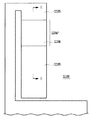
図1は上記特許文献に記載されたような記録ヘッド用基板に配置される1つの発熱部付近の一般的な構成を示す模式的平面図である。基板1100上において、発熱抵抗体層1104の上層に電極配線層1105が形成され、電極配線層1105の一部を除去してその部分の発熱抵抗体層を露出することで発熱部1104’が形成される。電極配線のパターンは基板1100上で引き回され、駆動素子回路ないし外部電源端子に接続されて、外部からの電力供給を受けることができる。ここで、発熱抵抗体層1104は電気抵抗値が高い材料で形成されており、電極配線層1105を介して外部から電流を流すことによって、電極配線層1105の非存在部分である発熱部1104’が熱エネルギーを発生し、インクを発泡させる。
FIG. 1 is a schematic plan view showing a general configuration in the vicinity of one heat generating portion disposed on a recording head substrate as described in the above-mentioned patent document. On the
図2は、図1の液路に相当する部分のII−II線で切断したインクジェット記録ヘッド用基板1100の模式的断面図である。図2において、1101はSiの基体、1102は熱酸化膜からなる蓄熱層、1103は蓄熱機能を兼ねるSiO膜やSiN膜等からなる層間膜である。層間膜1103上には発熱抵抗体層1104が、さらにその上層にAl,Al−Si,Al−Cu等の金属でなる電極配線層電極配線層1105が形成され、電極配線層1105の一部を除去してその部分の発熱抵抗体層を露出することで発熱部1104’が形成される。電極配線層1105は基板1100上で引き回され、駆動素子回路ないし外部電源端子に接続されて、外部からの電力供給を受けることができる。
FIG. 2 is a schematic cross-sectional view of the ink jet
さらに、発熱部1104'および電極配線層1105の上層として、それらをインクから保護および絶縁するためのSiO膜あるいはSiN膜等からなる保護層1106が設けられる。また、その上層に、インクの発泡に伴う化学的衝撃や物理的衝撃等によるダメージに耐える膜として高耐久保護膜1107が形成され、発熱部1104’上方の高耐久保護膜1107がインクに接する部位が熱作用部1108となる。
Further, a
ところで、インクジェット記録装置には、その普及に伴って、近年さらなる記録の高解像化、高画質化、高速化が求められている。このうち高解像化、高画質化の要求に対する一つの解決手段としては、1ドット当りの吐出インク量をより少なく(インクを滴として吐出する場合にはインク滴の小径化)することが挙げられる。従来、インクの小液滴化を達成するためには、ノズルの形状を変える(オリフィス面積を小さくする)とともに発熱部の面積を小さくすることで対応してきた。 By the way, along with the widespread use of ink jet recording apparatuses, in recent years, higher recording resolution, higher image quality, and higher speed are required. One solution to the demand for higher resolution and higher image quality is to reduce the amount of ink ejected per dot (when ink is ejected as droplets, the diameter of the ink droplet is reduced). It is done. Conventionally, in order to achieve a reduction in ink droplets, the shape of the nozzle is changed (the orifice area is reduced) and the area of the heat generating portion is reduced.
また、高速記録の要求に対する解決手段としては、電気熱変換素子を駆動する電気パルスの幅を短くすることにより駆動周波数を上げたり、インクを吐出させるノズル数を増やしたりすることで、短時間に多数のインク吐出を可能にすることが有効とされている。しかしながら、この解決手段を採ると、発熱抵抗体で発生した熱が基板に蓄積され、ヘッドの昇温をもたらすことになるので、場合によっては記録動作を中断させなければならなくなることもあり、記録のスループットが低下するという新たな問題が発生する。 As a solution to the demand for high-speed recording, the drive frequency can be increased by shortening the width of the electric pulse for driving the electrothermal transducer, or the number of nozzles for ejecting ink can be increased in a short time. It is effective to enable a large number of ink ejections. However, if this solution is adopted, the heat generated by the heating resistor is accumulated on the substrate, leading to a rise in the temperature of the head, and in some cases, the recording operation may have to be interrupted. A new problem arises in that the throughput of the system decreases.
そこで、発熱抵抗体で発生した熱を効率的にインクに作用させ、インクの吐出に利用するように膜構成を工夫する試みがなされている。 Therefore, an attempt has been made to devise a film structure so that heat generated by the heating resistor is efficiently applied to ink and used for ink discharge.
例えば、発熱抵抗体とインクに接する面との間の膜の厚さが薄いほど熱伝導性が良好となり、インク側以外へ逃げる熱量が減るため、記録ヘッドの蓄熱ないしは昇温の問題を抑制することができ、かつ発泡を生じさせるための消費電力も少なくてすむ。すなわち、発熱抵抗体上の保護層の実効的な厚みが薄いほどエネルギー効率がよくなる。ところが一方、保護層が薄すぎると、保護層に存在するピンホールが発熱抵抗体を露出させたり、配線の段差部を十分にカバーすることができなくなるために段差部の被覆不足を生じさせたりしてしまう。この結果、そこからインクが侵入し、配線の腐食や発熱抵抗体の腐食を引き起こし、その結果、信頼性の低下および寿命の低下が発生する。 For example, the thinner the film between the heating resistor and the surface in contact with the ink, the better the thermal conductivity, and the amount of heat that escapes to other than the ink side decreases. And less power consumption to cause foaming. That is, energy efficiency improves as the effective thickness of the protective layer on the heating resistor decreases. On the other hand, if the protective layer is too thin, pinholes present in the protective layer may expose the heating resistor, or the stepped portion of the wiring cannot be sufficiently covered, resulting in insufficient coverage of the stepped portion. Resulting in. As a result, ink penetrates from there, causing corrosion of the wiring and heating resistor, resulting in a decrease in reliability and a decrease in life.
このような問題に対処したものとして、第1および第2の保護層を設け、熱作用部においては第1の保護層を除去することにより、エネルギー効率を向上させて消費電力を下げ、かつ、保護層としての信頼性を上げ寿命を伸ばすことを可能とした構成が特許文献3に開示されている。 As a countermeasure against such a problem, the first and second protective layers are provided, and by removing the first protective layer in the heat acting part, the energy efficiency is improved and the power consumption is reduced, and Patent Document 3 discloses a configuration that can increase the reliability as the protective layer and extend the life.
図3は特許文献3に開示されたインクジェットヘッド用基板の熱作用部付近の模式的断面図である。この構成では、電極配線層1105の上層として第1保護層1106aおよび第2保護層1106bが形成されており、下層である第1保護層1106aが発熱部1108の上方において除去されている。すなわち、SiO膜,SiN膜等からなる第1保護層1106aを形成した後、パターニング等により熱作用部のみ第1保護層1106aを除去し、さらにSiO膜,SiN膜等からなる第2保護層1106bを形成し、最後に高耐久保護膜1107を形成したものである。このように、熱作用部1108における実質的な保護層を薄膜化することにより、発熱抵抗体層1104からの熱エネルギーは第2保護層1106bおよび高耐久保護膜1107のみを介してインクに伝達できるため、熱エネルギーを一層有効に利用することができるようになる一方、第2保護層1106bにより所要の保護絶縁機能を得ている。
FIG. 3 is a schematic cross-sectional view of the vicinity of the thermal action portion of the ink jet head substrate disclosed in Patent Document 3. As shown in FIG. In this configuration, the first
ここで、インクジェット記録ヘッドの系全体のエネルギーロスを少なくする上では、電極配線層の膜厚を厚くすることにより電極配線の抵抗値を下げることが有効である。しかしながら、その膜厚を厚くすることは、パターニングにより形成される段差部が高くなることを意味し、これらの段差部のカバレッジ性を考慮すれば保護膜をある程度厚くせざるを得ない。 Here, in order to reduce the energy loss of the entire system of the ink jet recording head, it is effective to reduce the resistance value of the electrode wiring by increasing the film thickness of the electrode wiring layer. However, increasing the film thickness means that the stepped portion formed by patterning becomes higher. If the coverage of these stepped portions is taken into consideration, the protective film must be thickened to some extent.
すると、図3に示した構成では、第1保護層1106aは、発熱部1104’に面する電極配線層1105の端部における段差を十分にカバーするために、当該端部より発熱部の内側に偏倚した部位で除去される。ここで、発熱部は全面に亘って発熱するが、発熱部の周縁部は熱の逃げが大きくなることから、発熱部の周縁から数μm程度内側までの領域を除いた領域(この領域を有効発泡領域と称す)のみしか発泡が生じないことが知られている。上記特許文献3に開示された構成を採用する場合、発熱部1104’に面する電極配線層1105の端部より発熱部の内側に偏倚した部位で第1保護層1106aが除去されている。換言すれば、発熱部の内側に偏倚した位置まで第1保護層1106aが存在する。このため、実際の有効発泡領域がさらに限局されて小さくなり、熱効率を低下させてしまう。すなわち、発熱部の小面積が求められる状況下、特許文献3に開示の技術をそのまま採用したのでは、熱効率をさらに低下させてしまうという問題点が生じるのである。
Then, in the configuration shown in FIG. 3, the first
一方、発熱抵抗体の抵抗値を高くし、インクジェット記録ヘッドの系全体に流れる電流値を少なくすることにより、配線部等で発生する熱エネルギーロスを抑える試みもなされている。この発熱抵抗体の高抵抗化の要求に対しては、各種材料検討や発熱抵抗体の膜厚を薄くする方法が試みられている。膜厚を薄くすることは製造安定性、特性安定性および信頼性等の諸特性を満足することが困難ではあるが、膜厚を薄くしつつも上記諸特性を満足するものが強く要望されている。 On the other hand, attempts have been made to suppress thermal energy loss that occurs in the wiring portion and the like by increasing the resistance value of the heating resistor and decreasing the value of the current flowing through the entire system of the ink jet recording head. In response to the demand for higher resistance of the heating resistor, various materials have been examined and methods for reducing the thickness of the heating resistor have been attempted. Although it is difficult to reduce the film thickness to satisfy various characteristics such as manufacturing stability, characteristic stability, and reliability, there is a strong demand for satisfying the above characteristics while reducing the film thickness. Yes.
しかるに、図3に示すような構成では、発熱抵抗体層上に電極配線層を積層した後に電極配線のパターニングが行われ、さらに第1保護層1106aの積層後にもそのパターニングが行われることで発熱部が形成される。従って、発熱抵抗体層の表面はこれらのパターニングに適用されるエッチング工程等の影響を受ける。すなわち、ドライエッチングが行われる場合にはプラズマに、ウェットエッチングが行われる場合にはエッチング液にさらされることになる。また、それらエッチング工程を実施するための搬送時に大気にさらされることもある。これらによって発熱抵抗体層の表面は、酸化されたり、エッチングによるダメージを受けたり、ガスや水分を吸着したりすることになり、この結果、抵抗値の変動やばらつきが生じることがあった。また、部分的な酸化やダメージによって信頼性が低下してしまうこともあった。このように、高抵抗化のために発熱抵抗体層の膜厚を薄くする一方、図3のような構成を得る場合は特に、上記諸特性を満足することが難しいものとなる。さらに、抵抗値のばらつきによって各ヒーターで発泡現象に違いが生じてしまうと、1吐出口での所要のインク吐出量を確保できないばかりか、各吐出口間でもインク吐出量が大きくばらつくことになり、記録品位の低下につながってしまうことになる。
However, in the configuration as shown in FIG. 3, the electrode wiring layer is patterned after the electrode wiring layer is stacked on the heating resistor layer, and further, the patterning is also performed after the first
本発明の主たる目的は、従来のインクジェット記録ヘッド用基板について上述した諸問題を解決し、発熱抵抗体で発生した熱エネルギーを高効率にインクに伝達でき、消費電力の削減を可能とすることを目的とする。 SUMMARY OF THE INVENTION The main object of the present invention is to solve the problems described above with respect to a conventional substrate for an ink jet recording head, to transfer heat energy generated by a heating resistor to ink with high efficiency, and to reduce power consumption. Objective.
本発明の他の目的は、製造工程に起因した抵抗値のばらつきが少なく、長期にわたって抵抗値が安定であり、信頼性の高いインク吐出動作を可能とすることにある。 Another object of the present invention is to provide a highly reliable ink discharge operation with little variation in resistance value caused by the manufacturing process, stable resistance value over a long period of time, and high reliability.
本発明のさらに他の目的は、以上により小型にして吐出口が高密度配置された信頼性の高いインクジェットヘッドを提供することにある。 Still another object of the present invention is to provide a highly reliable ink jet head in which discharge ports are arranged at high density with a smaller size.
そのために、本発明は、通電に応じてインクを吐出するために利用される熱エネルギーを発生する発熱部を有するインクジェットヘッド用基板の製造方法であって、
基体上に、第1の間隙を介して対をなす電極配線層を設ける工程と、
前記電極配線層の対および前記第1の間隙の上に、通電することで熱を発生する発熱抵抗材料層を設ける工程と、
該発熱抵抗材料層の上に、絶縁材料からなる第1の保護材料層を設ける工程と、
前記発熱抵抗材料層と前記第1の保護材料層とをエッチング法を用いて一括してパターニングして、前記電極配線層の対の一方から他方にわたり、前記発熱抵抗体層から前記第1の間隙に対応する部分が前記発熱部として用いられる発熱抵抗体層と、前記第1の保護材料層から前記発熱部を保護するために用いられる第1保護層と、を設ける工程と、
前記第1保護層の上と前記電極配線層の上とに、絶縁材料からなる第2の保護材料層を設ける工程と、
前記第2の保護材料層の一部をエッチングにより除去することで、前記第1の間隙の上側に前記第1の間隙より広い第2の間隙を有し、少なくとも前記電極配線を保護するために用いられる第2保護層を設ける工程と、
を具えたことを特徴とする。
Therefore, the present invention is a method for manufacturing a substrate for an inkjet head having a heat generating part that generates thermal energy used for discharging ink in response to energization,
Providing a pair of electrode wiring layers on the base via the first gap;
Providing a heating resistance material layer that generates heat when energized over the pair of electrode wiring layers and the first gap ;
Providing a first protective material layer made of an insulating material on the heating resistance material layer;
The heating resistor material layer and the first protective material layer are collectively patterned using an etching method, and the electrode wiring layer pair extends from one side to the other to the first gap. A step of providing a heating resistor layer in which a portion corresponding to the heating part is used as the heating part, and a first protective layer used to protect the heating part from the first protective material layer;
Providing a second protective material layer made of an insulating material on the first protective layer and on the electrode wiring layer;
By removing a part of the second protective material layer by etching, a second gap wider than the first gap is provided above the first gap, and at least to protect the electrode wiring Providing a second protective layer to be used ;
It is characterized by comprising.
本発明によれば、まず基本的には保護層を2層化し、インクジェットヘッドの電力消費に関与する領域である発熱部上において実質的な保護層の厚みを薄くするべくその一方(第2保護層)を除去することにより、熱効率を向上して、消費電力を低下することが可能となる。また、電極配線層上に発熱抵抗体層を配置したことにより、一方の保護層(第2保護層)を除去する際のパターニングを、発熱部を形成する電極配線の間隙より広い範囲で実施することが可能となり、有効発泡領域の減少が生じることなく、記録の高解像化や高画質化等を達成するための発熱部の小面積化を図ることができる。 According to the present invention, first, the protective layer is basically divided into two layers, and one of them (the second protective layer) is formed so as to reduce the thickness of the substantial protective layer on the heat generating portion which is an area related to the power consumption of the inkjet head. By removing the layer, the thermal efficiency can be improved and the power consumption can be reduced. In addition, since the heating resistor layer is disposed on the electrode wiring layer, the patterning when removing one of the protective layers (second protective layer) is performed in a range wider than the gap between the electrode wirings forming the heat generating portion. This makes it possible to reduce the area of the heat generating portion for achieving high resolution and high image quality of recording without reducing the effective foaming area.
さらに、発熱抵抗体層は電極配線上に形成され、また第2保護層の除去時に第1保護層に覆われたものとなるので、発熱抵抗体層の発熱部は製造工程に起因した抵抗値のばらつきが少なく、長期にわたって抵抗値が安定であり、信頼性の高いインク吐出動作を可能とするものとなる。 Further, since the heating resistor layer is formed on the electrode wiring and is covered with the first protective layer when the second protective layer is removed, the heating portion of the heating resistor layer has a resistance value resulting from the manufacturing process. The resistance value is stable over a long period of time, and a highly reliable ink ejection operation is possible.
また、以上により小型にしてノズルが高密度配置された信頼性の高いインクジェットヘッドを提供できる。 In addition, it is possible to provide a highly reliable ink jet head with a smaller size and high density nozzle arrangement.
以下、図面を参照して本発明を詳細に説明する。但し、本発明は、以下に説明する各実施形態のみに限定されるものでなく、本発明の目的を達成し得るものであれば、特許請求の範囲を逸脱することなく適宜の構成を採用してもよいことは勿論である。 Hereinafter, the present invention will be described in detail with reference to the drawings. However, the present invention is not limited to the embodiments described below, and any appropriate configuration can be adopted without departing from the scope of the claims as long as the object of the present invention can be achieved. Of course, it may be.
(インクジェットヘッド用基板の実施形態およびその製造工程)
図4および図5は、それぞれ、本発明の第1の実施形態によるインクジェットヘッド用基板の熱作用部周辺の模式的平面図およびそのV−V線断面図である。ここで、図1〜図4の各部と同様に機能する部分については対応箇所に同一符号を付してある。
(Embodiment of inkjet head substrate and manufacturing process thereof)
4 and 5 are a schematic plan view and a VV line sectional view of the vicinity of the thermal action section of the ink jet head substrate according to the first embodiment of the present invention, respectively. Here, parts that function in the same manner as the parts in FIGS. 1 to 4 are given the same reference numerals.
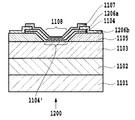
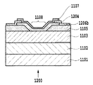
本実施形態では、まず基本的には保護層を2層化(1206a、1206b)した構成を採用し、インクジェットヘッドの電力消費に関与する領域である発熱部1104’上において実質的な保護層の厚みを薄くするべく、その一方を除去している。特に本実施形態では、基体1101に蓄熱層1102を介して形成した層間膜1103の上に電極配線層1105のパターニングを実施した後に、すなわち電極配線層1105上に、発熱抵抗体層1104を配置し、さらに第1および第2保護層1206aおよび1206bを配置した上で、発熱部1104’の上方の部位で第2保護層1206bを除去している。
In the present embodiment, first, a configuration in which the protective layer is made into two layers (1206a, 1206b) is adopted, and a substantial protective layer is formed on the
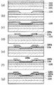
図6(a)〜(g)を参照して、図4および図5に示したインクジェットヘッド用基体の製造方法の実施形態を説明する。 With reference to FIGS. 6A to 6G, an embodiment of a method of manufacturing the ink jet head substrate shown in FIGS. 4 and 5 will be described.
まず、基体1101としてはSi基板あるいは既に駆動用のICを作り込んだSi基板を用いる。この基体としては、発熱部を形成する面のSi結晶方位が<100>のものを用いる。そして図6(a)に示すように、基体1101上に熱酸化により膜厚1.8μmの蓄熱層1102を形成し、さらに蓄熱層を兼ねる層間膜1103としてSiO2膜をプラズマCVD法などにより膜厚1.2μmに形成した。そして、電極配線層1105となるAl層をスパッタリングにより約400nmの厚さに形成した。
First, as the
次に、図6(b)に示すように、フォトリソグラフィ法を用いてドライエッチングを施し、発熱部を構成するための部分を含めてパターニングを行い、電極配線層1105を形成した。なお、パターニングされた電極配線層の端部は、後の工程で形成される膜のカバレッジ性を向上させるために、テーパ形状とすることが好ましい。
Next, as shown in FIG. 6B, dry etching was performed using a photolithography method, and patterning was performed including a portion for forming the heat generating portion, so that an
次に、Ta−Siからなる合金ターゲットを用いた反応性スパッタリング法により、発熱抵抗体層1104となるTaSiN膜を形成した。このとき、図7について後述するような成膜装置を用い、ガス流量をArガス42sccm、N2ガス8sccmとしてN2ガス分圧比を16%とし、ターゲットに投入するパワーを500W、雰囲気温度を200℃、基板温度を200℃として、40nmの厚さに形成した。続いて、真空雰囲気を維持したまま基板を別の成膜室へ搬送し、スパッタリング法を用いて第1保護層1206aとなるSiO2膜を形成した。このときのガス流量をArガス50sccm、ターゲットに投入するパワーを500W、雰囲気温度を200℃、基板温度を200℃として、200nmの厚さに形成した(図6(c))。
Next, a TaSiN film to be the
続いて、フォトリソグラフィ法を用いてエッチングを実施し、図6(d)に示すように、発熱抵抗体層1104と第1保護層1206aとを同時にパターニングした。
Subsequently, etching was performed using a photolithography method, and the
次に、プラズマCVD法を用いて第2保護層1206bとなるP−SiO膜を形成した(図6(e))。なお、第2保護層1206bは、パターン形成された電極配線層1105や発熱抵抗体層1104および第1保護層1206aの上に形成され、インクの侵入を防止する機能を有する。従って、膜の応力によるクラックの発生や基板の変形が生じない範囲で厚くすることが好ましい。膜厚としては300nm以上5μm以下、好ましくは500nm以上1μm以下程度が用いられ、本例では600nmの厚さとした。
Next, a P—SiO film to be the second
続いてフォトリソグラフィ法により第2保護層1206bのパターニングを行って、20μm×20μmの大きさの熱作用部が得られるようにした(図6(f))。すなわち、本例における熱作用部は、基本的に第2保護層1206bをエッチングにより除去することで形成される。つまり、前述したように発熱抵抗体層1104の発熱部1104'で発生した熱エネルギーを有効に利用するために、発熱部1104'上の熱作用部における保護膜は薄くすることが強く望ましく、本実施形態では第2保護層1206bを除去した構成が用いられている。これには、所望の熱作用部を形成するようにパターン形成する方法が用いられ、ドライエッチング法あるいはウェットエッチング法を用いる。この際に、第2保護層1206bの下層には膜質的に第2保護層1206bに対して密である第1保護層1206aが形成されており、十分なエッチング選択比をもって第2保護層1206bをエッチングすることが可能である。
Subsequently, the second
本例の除去工程では、バッファード沸酸を用いてウェットエッチングを行い、第2保護層1206bがエッチングされた時点でエッチング工程を完了させるようにした。バッファード沸酸に対するエッチングレートは、第1保護層1206aをなすSiO2膜で約50〜150nm/分、第2保護層1206bとなるP−SiO膜で約200〜500nm/分程度であり、十分なエッチング選択比をもって第2保護層1206bのパターニングが可能である。
In the removal process of this example, wet etching was performed using buffered hydrofluoric acid, and the etching process was completed when the second
最後に、スパッタリング法により高耐久保護層1107となるTa膜を200nmの厚さに形成し(図6(g))、パターニングを行って図5に示す基板1200を得た。なお、Ta層は保護層に比べ熱伝導率が高く、熱効率を大きく低下させるものではない。また、高耐久保護層1107は、緻密で膜厚の薄い第1保護層1206aの上に直接的に形成されることから、発熱部1104'からの熱エネルギーを熱作用部1107に効率よく伝導し、有効に発泡ないしインク吐出のために作用させることができる。
Finally, a Ta film to be a high durability
以上の工程によれば、次のような顕著な効果が得られる。
まず、電極配線層1105は、発熱部1104’に面する端部による段差の外側部分を含めて発熱抵抗層1104および第1保護層1206aで被覆されるため、第2保護絶縁膜1206bを除去する際のパターニングを当該端部より外側、すなわち発熱部1104’を形成するための電極配線1105の間隙より広い範囲で実施することが可能となる。従って、図3の従来例のように発熱部1104’の内側に偏倚した部位で第1保護層1106aを除去する場合に比べ、有効発泡領域の減少が生じない。このような構成は、吐出インク量を少量化して記録の高解像化や高画質化等を達成するために発熱部の小面積化を図る場合に特に有効である。
According to the above process, the following remarkable effects are obtained.
First, since the
また、本実施形態では、先にパターニングされた電極配線1105上に発熱抵抗層1104と第1保護膜1206aとが連続的に形成される。これにより発熱抵抗層が、発熱抵抗体層上に電極配線層を積層した後にそのパターニングを行い、さらに第1保護層1206aの積層後にもそのパターニングを行うことで発熱部が形成される従来例のように、エッチング工程等の影響を受けることがない。そのため、本実施形態の発熱抵抗体層の表面は、酸化されたり、エッチングによるダメージを受けたり、ガスや水分を吸着したりすることがなく、この結果、抵抗値の変動やばらつきを格段に少なくすることが可能となる。そしてこれは、特に発熱抵抗層の高抵抗化のために膜厚を薄くする場合においてよりよい効果をもたらすものとなる。
In the present embodiment, the
なお、上記工程において、本実施形態における発熱抵抗層は各種成膜法で作製可能であるが、一般的には電源として高周波(RF)電源または直流(DC)電源を用いたマグネトロンスパッタ装置を適用して形成することができる。 In the above process, the heating resistance layer in the present embodiment can be manufactured by various film forming methods. Generally, a magnetron sputtering apparatus using a radio frequency (RF) power source or a direct current (DC) power source as a power source is applied. Can be formed.
図7はかかるスパッタリング装置の概要を示す。図7において、4001はあらかじめ所定の組成に作製されたターゲット、4002は平板マグネット、4011は基板への成膜を制御するシャッター、4003は基板ホルダー、4004は基板、4006はターゲット4001と基板ホルダー4003に接続された電源である。4008は成膜室4009の外周壁を囲んで設けられた外部ヒーターである。外部ヒーター4008は、成膜室4009の雰囲気温度を調節するのに使用される。基板ホルダー4003の裏面には、基板の温度制御を行う内部ヒーター4005が設けられている。基板4004の温度制御は外部ヒーター4008および内部ヒーター4005を併用して行うことが好ましい。
FIG. 7 shows an outline of such a sputtering apparatus. In FIG. 7,
図7の装置を用いた成膜は、以下のように行われる。
まず、排気ポンプ4007を用いて成膜室4009を1×10⁻⁵〜1×10⁻⁶Paまで排気する。次いで、アルゴンガスあるいは形成する発熱抵抗体に応じて窒素ガス、酸素ガス、炭素系ガスからなる混合ガスを、マスフローコントローラー(不図示)を介してガス導入口4010から成膜室4009に導入する。このとき、上記基板温度および雰囲気温度が所定の温度になるように内部ヒーター4005および外部ヒーター4008を調節する。次に、電源4006からターゲット4001にパワーを印加してスパッタリング放電を行い、シャッター4011を調節して、基板4004の上に薄膜を形成させる。
Film formation using the apparatus of FIG. 7 is performed as follows.
First, the
さらに、保護層1206aを形成するための膜についても、上記発熱抵抗層と同様に作製可能である。
Further, a film for forming the
また、上述した例では、発熱抵抗体層1104をTaSiNの膜で形成するものとしたが、TaAl,HfB2等の合金系材料やTaN,TaSiO,CrSiO,TiSiC等の膜を反応性スパッタリング法により形成するものでもよい。さらに、発熱抵抗層としてはその他にPoly−Si系材料等を用いるものでもよく、所要の発熱機能を果たし得るものであれば、その材料は特に限定されるものではない。
In the example described above, the
(インクジェットヘッドの構成および製造工程)
続いて、上記実施形態に係る基板を用いて構成されるインクジェット記録ヘッドについて説明する。
図8はインクジェット記録ヘッドの模式的な斜視図である。
このインクジェット記録ヘッドは、所定のピッチで熱作用部1108が形成された発熱部列を2列、並列させてなる基板1200を有している。ここで、上記製造工程を経て製造された2枚の基板を、熱作用部1108が配列されている側の縁部を対向配置することで当該並列化が行われるようにしてもよいし、1枚の基体上に予め発熱部が2列並列するように上記製造工程を実施してもよい。
(Configuration and manufacturing process of inkjet head)
Next, an ink jet recording head configured using the substrate according to the embodiment will be described.
FIG. 8 is a schematic perspective view of the ink jet recording head.
This ink jet recording head has a
この基板1200に対しては、熱作用部1108に対応したインク吐出口5と、外部から導入されたインクを貯留する液室部分(不図示)と、吐出口5のそれぞれに対応して液室からインクを供給するためのインク供給口9と、吐出口5と供給口9とを連通する流路とが形成された部材(オリフィスプレート)4が接合されて、インクジェット記録ヘッド410が構成される。
For the
なお、図8では、各列の熱作用部1108およびインク吐出口5が、線対称に配置されているように描かれているが、各列の熱作用部1108およびインク吐出口5を互いに半ピッチずらして配置することで、記録の解像度をさらに高めることができる。
In FIG. 8, the
図9(a)〜(d)は図8のインクジェット記録ヘッドを製造する工程を示す模式的断面図である。 9A to 9D are schematic cross-sectional views showing the steps for manufacturing the ink jet recording head of FIG.
基板1200を構成するための基体1101としては、発熱部を形成する面のSi結晶方位が<100>のものを用いることは上述した。かかる基板1200の裏面のSiO2膜307上に、インク供給口310を形成するためのマスクであって耐アルカリ性を有するマスク剤でなるSiO2膜パターニングマスク308を形成する。SiO2膜パターニングマスク308は、例えば以下のようにして形成する。
As described above, as the
まず、SiO2膜パターニングマスク108となるマスク剤をスピンコートなどによって基板1200の裏面に全面塗布し、熱硬化させる。そして、その上にポジ型レジストをスピンコートなどによって塗布し、乾燥させる。次に、このポジ型レジストをフォトリソグラフィ技術を用いてパターニングし、このポジ型レジストをマスクとして、SiO2膜パターニングマスク308となるマスク剤の露出された部分をドライエッチングなどによって除去する。最後にポジ型レジストを剥離して、所望のパターンのSiO2膜パターニングマスク308を得る。
First, a mask agent that becomes the SiO 2 film patterning mask 108 is applied to the entire back surface of the
次に、熱作用部1108が形成された面上に型材303を形成する。型材303は、後の工程で溶解して、それが設けられた部分をインク流路とするために形成するものである。すなわち、所望の高さおよび平面パターンのインク流路を形成するために、適切な高さおよび平面パターンに形成する。型材303の形成は、例えば次のようにして行うことができる。
Next, a
型材303の材料としては、例えば、ポジ型フォトレジストであるODUR1010(東京応化工業株式会社製、商品名)を用い、これをドライフィルムのラミネート,スピンコートなどによって基板1200上に所定の厚みで塗布する。次に、紫外線、Deep UV光などによって露光、現像を行うフォトリソグラフィー技術を用いてパターニングする。これによって、所望の厚みおよび平面パターンを有する型材303が得られる。
As the material of the
次に、図9(b)に示す工程で、前の工程で基板1200上に形成した型材303を被覆するように、オリフィスプレート4の素材をスピンコートなどによって塗布し、フォトリソグラフィー技術によって、所望の形状にパターニングする。そして、熱作用部1108上の所定の位置にインク吐出口5をフォトリソグラフィ技術によって開口する。また、インク吐出口5が開口するオリフィスプレート4の面には、ドライフィルムのラミネートなどによって撥水層306を形成する。
Next, in the step shown in FIG. 9B, the material of the orifice plate 4 is applied by spin coating or the like so as to cover the
オリフィスプレート4の形成材料としては、感光性エポキシ樹脂、感光性アクリル樹脂などを用いることができる。オリフィスプレート4は、インク流路を構成するものであり、インクジェット記録ヘッド使用時には常にインクと接触することになるので、その材料としては、特に、光反応によるカチオン重合性化合物が適している。また、オリフィスプレート4の材料としては、使用するインクの種類および特性によって耐久性などが大きく左右されるので、使用するインクによっては、上記の材料以外の相応の化合物を選択してもよい。 As a material for forming the orifice plate 4, a photosensitive epoxy resin, a photosensitive acrylic resin, or the like can be used. The orifice plate 4 constitutes an ink flow path, and is always in contact with ink when the ink jet recording head is used. Therefore, a cation polymerizable compound by photoreaction is particularly suitable as the material. Further, as the material of the orifice plate 4, durability and the like greatly depend on the type and characteristics of the ink to be used. Therefore, depending on the ink to be used, a corresponding compound other than the above materials may be selected.
次に、図9(c)に示す工程で、基板1200を貫通する貫通口であるインク供給口310の形成を行う際、インクジェット記録ヘッドの機能素子が形成された面や基板1200の側面にエッチング液が触れないように、樹脂からなる保護材311をスピンコートなどによって塗布することでこれらの部分を覆う。保護材311の材料としては、異方性エッチングを行う際に使用する強アルカリ溶液に対して十分な耐性を有する材料を用いる。このような保護材311によってオリフィスプレート4の上面側をも覆うことによって、撥水層306の劣化を防ぐことも可能となる。
Next, in the step shown in FIG. 9C, when forming the
次に、予め形成しておいたSiO2膜パターニングマスク308を用いて、SiO2膜307をウェットエッチングなどによってパターニングし、基板1200の裏面を露出するエッチング開始開口部309を形成する。
Next, the SiO 2 film 307 is patterned by wet etching or the like using a previously formed SiO 2
次に、図9(d)に示す工程で、SiO2膜307をマスクとした異方性エッチングによってインク供給口310を形成する。該異方性エッチングに用いるエッチング液としては、例えばTMAH(テトラメチルアンモニュウムハイドロオキサイド)溶液などの強アルカリ溶液を用いる。そして、例えば、TMAHの22重量%溶液を、その温度を80℃に保ちながら所定時間(十数時間)、エッチング開始開口部309からSi基板1200に付与することによって貫通口を形成する。
Next, in the step shown in FIG. 9D, the
最後に、SiO2膜パターニングマスク308と保護材311を除去する。そして、更に、型材303を溶解させ、インク吐出口5とインク供給口9あるいは310から溶出させて除去し、乾燥させる。型材303の溶出は、Deep UV光によって全面露光を行った後、現像を行うことによって実施でき、必要に応じて現像の際、超音波浸漬すれば、実質的に完全に型材303を除去することができる。
Finally, the SiO 2
以上で、インクジェット記録ヘッドの主要な製造工程が完了し、図8に示した構成が得られる。なお、以上の実施形態で作成された基板およびこれを用いる記録ヘッドを第1実施例による基板および記録ヘッドとし、その評価を後述のように行うものとする。 Thus, the main manufacturing process of the ink jet recording head is completed, and the configuration shown in FIG. 8 is obtained. In addition, the board | substrate produced in the above embodiment and the recording head using this are made into the board | substrate and recording head by 1st Example, and the evaluation shall be performed as mentioned later.
(インクジェット記録ヘッドカートリッジおよび記録装置)
このインクジェット記録ヘッドは、プリンタ、複写機、通信システムを有するファクシミリ、プリンタ部を有するワードプロセッサなどの装置、更には各種処理装置と複合的に組み合わせた産業記録装置に搭載可能である。そして、このインクジェット記録ヘッドを用いることによって、紙、糸、繊維、布帛、皮革、金属、プラスチック、ガラス、木材、セラミックスなど種々の記録媒体に記録を行うことができる。なお、本明細書において、「記録」とは、文字や図形などの意味を持つ画像を記録媒体に対して付与することだけでなく、パターンなどの意味を持たない画像を付与することも意味する。
(Inkjet recording head cartridge and recording apparatus)
The ink jet recording head can be mounted on an apparatus such as a printer, a copying machine, a facsimile having a communication system, a word processor having a printer unit, or an industrial recording apparatus combined with various processing apparatuses. By using this ink jet recording head, recording can be performed on various recording media such as paper, thread, fiber, fabric, leather, metal, plastic, glass, wood, and ceramics. In this specification, “recording” means not only giving an image having a meaning such as a character or a figure to a recording medium but also giving an image having no meaning such as a pattern. .
以下、上記インクジェット記録ヘッドをインクタンクと一体化してなるカートリッジ形態のユニットおよびこれを用いるインクジェット記録装置について説明する。 Hereinafter, a cartridge type unit in which the ink jet recording head is integrated with an ink tank and an ink jet recording apparatus using the unit will be described.
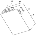
図10は上記したインクジェット記録ヘッドを構成要素に含むインクジェット記録ヘッドユニットの構成例を示す。図中、402はインクジェット記録ヘッド部410に電力を供給するための端子を有するTAB(Tape Automated Bonding)用のテープ部材であり、プリンタ本体から接点403を介して電力を供給する。404はインクをヘッド部410に供給するためのインクタンクである。すなわち、図10のインクジェット記録ヘッドユニットは、記録装置に装着可能なカートリッジの形態を有するものである。
FIG. 10 shows a configuration example of an inkjet recording head unit including the above-described inkjet recording head as a component. In the figure,
図11は図10のインクジェット記録ヘッドユニットを用いて記録を行うインクジェット記録装置の概略構成例を示すものである。 FIG. 11 shows a schematic configuration example of an ink jet recording apparatus that performs recording using the ink jet recording head unit of FIG.
図示のインクジェット記録装置において、キャリッジ500は無端ベルト501に固定され、かつガイドシャフト502に沿って移動可能になっている。無端ベルト501はプーリ503および504に巻回され、プーリ503にはキャリッジ駆動モータ504の駆動軸が連結されている。従って、キャリッジ500は、モータ504の回転駆動に伴いガイドシャフト502に沿って往復方向(A方向)に主走査される。
In the illustrated ink jet recording apparatus, a
キャリッジ500上には、上記カートリッジ形態のインクジェット記録ヘッドユニットが搭載されている。ここで、インクジェット記録ヘッドユニットは、ヘッド410の吐出口4が記録媒体としての用紙Pと対向し、かつ上記配列方向が主走査方向と異なる方向(例えば用紙Pの搬送方向である副走査方向)に一致するようにキャリッジ500に搭載される。なお、インクジェット記録ヘッド410およびインクタンク404の組は、使用するインク色に対応した個数を設けることができ、図示の例では4色(例えばブラック、イエロー、マゼンタ、シアン)に対応して4組設けられている。
On the
また、図示の装置には、キャリッジの主走査方向上の移動位置を検出するなどの目的でリニアエンコーダ506が設けられている。リニアエンコーダ506の一方の構成要素としてはキャリッジ500の移動方向に沿って設けられたリニアスケール507があり、このリニアスケール507には所定密度で、等間隔にスリットが形成されている。一方、キャリッジ500には、リニアエンコーダ506の他方の構成要素として、例えば、発光部および受光センサを有するスリットの検出系508および信号処理回路が設けられている。従って、リニアエンコーダ506からは、キャリッジ500の移動に伴って、インク吐出タイミングを規定するための吐出タイミング信号およびキャリッジの位置情報が出力される。
The illustrated apparatus is provided with a
記録媒体としての記録紙Pは、キャリッジ500のスキャン方向と直交する矢印B方向に間欠的に搬送される。記録紙Pは搬送方向上流側の一対のローラユニット509および510と、下流側一対のローラユニット511および512とにより支持され、一定の張力を付与されてインクジェット記録ヘッド410に対する平坦性を確保した状態で搬送される。各ローラユニットに対する駆動力は、図示しない用紙搬送モータから伝達される。
The recording paper P as a recording medium is intermittently conveyed in the direction of arrow B perpendicular to the scanning direction of the
以上のような構成によって、キャリッジ500の移動に伴いインクジェット記録ヘッド410の吐出口の配列幅に対応した幅の記録と用紙Pの搬送とを交互に繰り返しながら、用紙P全体に対する記録が行われる。
With the above-described configuration, recording on the entire sheet P is performed while alternately repeating the recording of the width corresponding to the array width of the ejection ports of the
なお、キャリッジ500は、記録開始時または記録中に必要に応じてホームポジションで停止する。このホームポジションには、各インクジェット記録ヘッド410の吐出口が設けられた面(吐出口面)をキャッピングするキャップ部材513が設けられ、このキャップ部材513には吐出口から強制的にインクを吸引して吐出口の目詰まり等を防止するための吸引回復手段(不図示)が接続されている。
The
(他の実施形態)
基板1200およびその製造工程としては、上述したものに限られることなく、種々のものを採用することができる。
(Other embodiments)
The
例えば、第1保護層1206aを形成するための膜については、上記発熱抵抗層と同様にして各種成膜法で作製可能であり、電源として高周波(RF)電源または直流(DC)電源を用いたマグネトロンスパッタリング法により形成可能である。このとき、基板に対して高周波(RF)電源または直流(DC)電源によりバイアスの電圧を印加することも可能であり、これによって、膜質的に密な膜を形成することができる。
For example, the film for forming the first
この場合は、上例と同様の製造工程を経て発熱抵抗体層1104となるTaSiN膜を形成し、真空雰囲気を維持したまま成膜装置の別の成膜室へ搬送した後、第1保護層1206aとしてSiO2膜を形成する際に、次の条件で成膜を行うことができる。すなわち、このときは、ガス流量をArガス50sccm、ターゲットに投入するパワーを500Wとし、基板にRFパワー100Wを印加しながら成膜を行うバイアススパッタリング法を用い、雰囲気温度を200℃、基板温度を200℃として、200nmの厚さに形成する。
In this case, a TaSiN film to be the
そして、以降は上例と同様の製造工程を経てインクジェット記録ヘッド用基体を得、さらに図9(a)〜(d)と同様にしてインクジェット記録ヘッドを得る。なお、かかる実施形態で作成された基板およびこれを用いる記録ヘッドを第2実施例による基板および記録ヘッドとし、その評価を後述のように行うものとする。 Thereafter, through the same manufacturing process as in the above example, an ink jet recording head substrate is obtained, and further, an ink jet recording head is obtained in the same manner as in FIGS. In addition, the board | substrate produced in this embodiment and the recording head using this are made into the board | substrate and recording head by 2nd Example, and the evaluation shall be performed as mentioned later.
また、第1保護層1206aの膜質をさらに向上させるために、ECR(Electron Cyclotron Reasonance:電子サイクロトロン共鳴)を用いたECRスパッタ法を用いることもできる。これは、成膜中のガス圧を低くすることができ、基板に飛び込む高エネルギー粒子を少なくすることができ、高純度で緻密な膜を形成することが可能である。
Further, in order to further improve the film quality of the first
この場合は、上例と同様の製造工程を経て発熱抵抗体層1104となるTaSiN膜を形成し、真空雰囲気を維持したまま成膜装置の別の成膜室へ搬送した後、ECRスパッタ法を用いて第1保護層1206aとなるSiO2膜を形成した。このとき、Arガスの圧力は約2.67×10⁻²Pa、マイクロ波電力は300W、基板温度は300℃とし、200nmの厚みの膜を形成した。
In this case, a TaSiN film to be the
そして、以降は上例と同様の製造工程を経てインクジェット記録ヘッド用基体を得、さらに図9(a)〜(d)と同様にしてインクジェット記録ヘッドを得た。なお、かかる実施形態で作成された基板およびこれを用いる記録ヘッドを第3実施例による基板および記録ヘッドとし、その評価を後述のように行うものとする。 Thereafter, through the same manufacturing steps as in the above example, an ink jet recording head substrate was obtained, and an ink jet recording head was obtained in the same manner as in FIGS. In addition, the board | substrate produced in this embodiment and the recording head using this are made into the board | substrate and recording head by 3rd Example, and the evaluation shall be performed as mentioned later.
さらに、以上では、発熱抵抗体層1104となる膜と第1保護層1206aとなる膜とを個別に形成したが、膜厚方向で連続的もしくは段階的に組成を変えながら成膜を行う手段を用いることにより、連続膜からなる層を一体的にかつ同時の工程で形成することも可能である。
Further, in the above, the film to be the
図12はかかる実施形態によるインクジェット記録ヘッド用基板の模式的断面図であり、発熱抵抗体層と第1保護層との両層の機能を果たす層1204が配置されている。ここで、発熱抵抗体としての機能を発揮させるための膜部分は、発熱抵抗体を形成するために用いる反応性ガス(発熱抵抗体に応じて窒素、酸素、炭化系ガス)の全体のガスに対する割合を比較的少なくして形成し、その後に連続して反応性ガスの割合を連続的または段階的に増加させることにより電気的に絶縁体となるように形成することで、保護層(第1保護層)としての機能を発揮する膜部分を構成することができる。
FIG. 12 is a schematic cross-sectional view of an ink jet recording head substrate according to such an embodiment, in which a
ここで、本実施形態の発熱抵抗体はαxβyγzで表わされる材料から構成され、αはTa、Ti、Zr、Cr、Mo、Hfから選ばれた1種以上の元素、βはSi、Bから選ばれた1種以上の元素、γはC,O,Nから選ばれた1種以上の元素(x+y+z=100%)とすることができる。そして、第1保護層について、βおよびγを発熱抵抗体と同じ元素とすることで、連続膜からなる層を一体的にかつ同時の工程で形成可能となる。 Here, the heating resistor of this embodiment is made of a material represented by αxβyγz, α is one or more elements selected from Ta, Ti, Zr, Cr, Mo, and Hf, and β is selected from Si and B. The one or more elements selected, γ, can be one or more elements selected from C, O, and N (x + y + z = 100%). And about a 1st protective layer, it becomes possible to form the layer which consists of a continuous film integrally and by the same process by making (beta) and (gamma) into the same element as a heating resistor.
例えば、発熱抵抗体をTaSiN、第1保護層をSiNとする場合、層1204は次のような工程にて形成可能である。
For example, when the heating resistor is TaSiN and the first protective layer is SiN, the
まず、上例と同様の製造工程を経て電極配線層1105を形成した後、2個のターゲットTaおよびSiを用いた2元同時スパッタリング法を適用し、膜厚方向で組成を変えることにより、発熱抵抗層と第1保護層1206aを連続的に形成する。すなわち、まず発熱抵抗体の機能を有する膜部分を形成する際、ガス流量をArガスについて42sccm、N2ガスについて8sccmとしてN2ガス分圧比を16%とし、ターゲットに投入するパワーをSiターゲットについては150W、Taターゲットについては500Wとし、雰囲気温度を200℃、基板温度を200℃として、厚さ30nmのTaSiN膜を形成する。次いで、第1保護層の機能を有する部分を形成するために、ガス流量をArガスについて42sccm、N2ガスについて25sccmとして窒素ガス分圧比を約37%とし、ターゲットに投入するパワーをSiターゲットについては500W、Taターゲットについては0Wとし、雰囲気温度を200℃、基板温度を200℃として、膜厚さ250nmのSiN膜に形成する。
First, after forming the
そして、以降は上例と同様の製造工程を経てインクジェット記録ヘッド用基体を得、さらに図9(a)〜(d)と同様にしてインクジェット記録ヘッドを得ることができる。なお、かかる実施形態で作成された基板およびこれを用いる記録ヘッドを第4実施例による基板および記録ヘッドとし、その評価を後述のように行うものとする。 Thereafter, through the same manufacturing process as in the above example, an ink jet recording head substrate is obtained, and further, an ink jet recording head can be obtained in the same manner as in FIGS. In addition, the board | substrate produced in this embodiment and the recording head using this are made into the board | substrate and recording head by 4th Example, and the evaluation shall be performed as mentioned later.
なお、本実施形態においては、反応性ガスの割合およびTaターゲットへの投入パワーを段階状に変化させるものとしたが、連続的に変化させることで膜の組成が厚み方向に連続的に変化するようにしてもよい。 In the present embodiment, the ratio of the reactive gas and the input power to the Ta target are changed stepwise, but the film composition changes continuously in the thickness direction by changing it continuously. You may do it.
(基板およびインクジェット記録ヘッドの評価)
実施例1〜実施例4によるインクジェット記録ヘッド用基体をそれぞれ連続して100枚作製し、ウエハ内の抵抗値の測定(ウエハ内で9ポイント)を行い、ロット間における抵抗値変動を調べた。
その結果を表1に示す。
(Evaluation of substrate and inkjet recording head)
100 substrates of the inkjet recording head according to each of Examples 1 to 4 were manufactured in succession, and the resistance value in the wafer was measured (9 points in the wafer) to check the resistance value variation between lots.
The results are shown in Table 1.

これに対し、図3のような構成ではウエハ内の抵抗値のばらつきは±4〜5%程度であった。このことから、本発明の各実施例による基板では抵抗値変動が少なく、効果のあることが明らかとなった。これは、本実施例においては、予めパター二ングされた電極配線上に発熱抵抗層と第1保護層が連続的に形成されるため、発熱抵抗層の表面が酸化されたり、エッチングによるダメージを受けたり、ガスや水分が吸着したりすることがないため、抵抗値の変動やばらつきが少ないことを示している。 On the other hand, in the configuration as shown in FIG. 3, the variation of the resistance value within the wafer was about ± 4 to 5%. From this, it was clarified that the substrate according to each example of the present invention has an effect that the resistance value fluctuation is small. In this embodiment, since the heating resistance layer and the first protective layer are continuously formed on the electrode wiring previously patterned, the surface of the heating resistance layer is oxidized or damaged by etching. This indicates that there is little fluctuation or variation in resistance value because no gas or moisture is absorbed.
次に、各実施例の基板を用いて構成した実施例1〜実施例4のインクジェット記録ヘッドをインクジェット記録装置に取り付けて、印字耐久試験を行った。この試験は、A4サイズの用紙に、インクジェット記録装置に組み込まれている一般的なテストパターンを記録させることで行った。このとき、駆動周波数15KHz、駆動パルス幅1μsのパルス信号を与え、吐出を開始する発泡開始電圧Vthを求めた。その結果を表2に示す。 Next, the ink jet recording heads of Examples 1 to 4 configured using the substrates of the respective examples were attached to the ink jet recording apparatus, and a printing durability test was performed. This test was performed by recording a general test pattern incorporated in an ink jet recording apparatus on A4 size paper. At this time, a pulse signal having a drive frequency of 15 KHz and a drive pulse width of 1 μs was given, and a foaming start voltage Vth for starting ejection was obtained. The results are shown in Table 2.
図3の構成において第2保護層を膜厚300nmとしたものではVth= 17.0Vであり、これに対し本実施例の第1保護層の膜厚を200nmとしたものでは、表2のような結果が得られ、Vthが約10〜15%程度低減され、消費電力の改善が見られた。 In the configuration of FIG. 3, when the thickness of the second protective layer is 300 nm, Vth = 17.0 V, whereas when the thickness of the first protective layer of this example is 200 nm, as shown in Table 2. As a result, Vth was reduced by about 10 to 15%, and power consumption was improved.
次に、このVthの1.3倍を駆動電圧Vopとし、1500文字の標準文書の記録を行ったところ、実施例1〜実施例4のいずれのヘッドにおいても、10000枚以上の記録が可能であることが確認され、かつ記録品位の劣化も見られなかった。すなわち、本発明を適用したインクジェット記録ヘッドでは長期にわたり画像が安定しており、耐久特性にも優れていることがわかった。 Next, when 1.3 times this Vth was used as the driving voltage Vop and a standard document of 1500 characters was recorded, 10,000 heads or more could be recorded with any of the heads of Examples 1 to 4. It was confirmed that there was no deterioration in recording quality. That is, it was found that the ink jet recording head to which the present invention is applied has stable images over a long period of time and excellent durability characteristics.
1100、1200、1300 インクジェット記録ヘッド用基板
1101 Si基体
1102 蓄熱層
1103 層間膜
1104 発熱抵抗体層
1104’ 発熱部
1105 電極配線層
1106a、1206a 第1保護層
1106b、1206b 第2保護層
1107 高耐久保護層
1108 熱作用部
410 インクジェットヘッド
1100, 1200, 1300 Inkjet
Claims (11)
基体上に、第1の間隙を介して対をなす電極配線層を設ける工程と、
前記電極配線層の対および前記第1の間隙の上に、通電することで熱を発生する発熱抵抗材料層を設ける工程と、
該発熱抵抗材料層の上に、絶縁材料からなる第1の保護材料層を設ける工程と、
前記発熱抵抗材料層と前記第1の保護材料層とをエッチング法を用いて一括してパターニングして、前記電極配線層の対の一方から他方にわたり、前記発熱抵抗体層から前記第1の間隙に対応する部分が前記発熱部として用いられる発熱抵抗体層と、前記第1の保護材料層から前記発熱部を保護するために用いられる第1保護層と、を設ける工程と、
前記第1保護層の上と前記電極配線層の上とに、絶縁材料からなる第2の保護材料層を設ける工程と、
前記第2の保護材料層の一部をエッチングにより除去することで、前記第1の間隙の上側に前記第1の間隙より広い第2の間隙を有し、少なくとも前記電極配線を保護するために用いられる第2保護層を設ける工程と、
を具えたことを特徴とするインクジェット記録ヘッド用基板の製造方法。 A method for manufacturing an ink jet head substrate having a heat generating part that generates thermal energy used to eject ink in response to energization,
Providing a pair of electrode wiring layers on the base via the first gap;
Providing a heating resistance material layer that generates heat when energized over the pair of electrode wiring layers and the first gap ;
Providing a first protective material layer made of an insulating material on the heating resistance material layer;
The heating resistor material layer and the first protective material layer are collectively patterned using an etching method, and the electrode wiring layer pair extends from one side to the other to the first gap. A step of providing a heating resistor layer in which a part corresponding to the heating part is used as the heating part, and a first protective layer used to protect the heating part from the first protective material layer;
Providing a second protective material layer made of an insulating material on the first protective layer and on the electrode wiring layer;
By removing a part of the second protective material layer by etching, a second gap wider than the first gap is provided above the first gap, and at least the electrode wiring is protected. Providing a second protective layer to be used ;
A method of manufacturing a substrate for an ink jet recording head, comprising:
Priority Applications (2)
| Application Number | Priority Date | Filing Date | Title |
|---|---|---|---|
| JP2004325534A JP4646602B2 (en) | 2004-11-09 | 2004-11-09 | Manufacturing method of substrate for ink jet recording head |
| US11/264,160 US7566116B2 (en) | 2004-11-09 | 2005-11-02 | Ink jet head circuit board, method of manufacturing the same and ink jet head using the same |
Applications Claiming Priority (1)
| Application Number | Priority Date | Filing Date | Title |
|---|---|---|---|
| JP2004325534A JP4646602B2 (en) | 2004-11-09 | 2004-11-09 | Manufacturing method of substrate for ink jet recording head |
Publications (3)
| Publication Number | Publication Date |
|---|---|
| JP2006130885A JP2006130885A (en) | 2006-05-25 |
| JP2006130885A5 JP2006130885A5 (en) | 2010-02-18 |
| JP4646602B2 true JP4646602B2 (en) | 2011-03-09 |
Family
ID=36315870
Family Applications (1)
| Application Number | Title | Priority Date | Filing Date |
|---|---|---|---|
| JP2004325534A Expired - Fee Related JP4646602B2 (en) | 2004-11-09 | 2004-11-09 | Manufacturing method of substrate for ink jet recording head |
Country Status (2)
| Country | Link |
|---|---|
| US (1) | US7566116B2 (en) |
| JP (1) | JP4646602B2 (en) |
Families Citing this family (10)
| Publication number | Priority date | Publication date | Assignee | Title |
|---|---|---|---|---|
| JP4208793B2 (en) * | 2004-08-16 | 2009-01-14 | キヤノン株式会社 | Inkjet head substrate, method for producing the substrate, and inkjet head using the substrate |
| JP4646602B2 (en) | 2004-11-09 | 2011-03-09 | キヤノン株式会社 | Manufacturing method of substrate for ink jet recording head |
| US8075102B2 (en) * | 2008-06-19 | 2011-12-13 | Canon Kabushiki Kaisha | Substrate for ink jet head and ink jet head |
| US9096059B2 (en) | 2012-12-27 | 2015-08-04 | Canon Kabushiki Kaisha | Substrate for inkjet head, inkjet head, and inkjet printing apparatus |
| JP6039411B2 (en) | 2012-12-27 | 2016-12-07 | キヤノン株式会社 | Inkjet head substrate, inkjet head, and inkjet head manufacturing method |
| JP6150519B2 (en) | 2012-12-27 | 2017-06-21 | キヤノン株式会社 | INKJET RECORDING HEAD SUBSTRATE, INKJET RECORDING HEAD, INKJET RECORDING HEAD MANUFACTURING METHOD, INKJET RECORDING DEVICE, AND INKJET RECORDING HEAD SUBSTRATE |
| JP6335436B2 (en) | 2013-04-26 | 2018-05-30 | キヤノン株式会社 | Method for manufacturing liquid discharge head |
| KR102283505B1 (en) | 2014-08-05 | 2021-07-30 | 삼성전자주식회사 | Semiconductor packages and Semiconductor modules |
| JP6516613B2 (en) | 2015-07-24 | 2019-05-22 | キヤノン株式会社 | Substrate for liquid discharge head and method of manufacturing substrate for liquid discharge head |
| JP7191669B2 (en) | 2018-12-17 | 2022-12-19 | キヤノン株式会社 | SUBSTRATE FOR LIQUID EJECTION HEAD AND MANUFACTURING METHOD THEREOF |
Citations (5)
| Publication number | Priority date | Publication date | Assignee | Title |
|---|---|---|---|---|
| JPH0655737A (en) * | 1991-10-15 | 1994-03-01 | Canon Inc | Base for liquid jet recording head and its manufacture, liquid jet recording head and liquid jet recording device |
| JPH06198889A (en) * | 1993-01-07 | 1994-07-19 | Fuji Xerox Co Ltd | Thermal control type ink-jet recording element |
| JP2003136738A (en) * | 2001-11-06 | 2003-05-14 | Canon Inc | Circuit board, liquid discharge head, and method for manufacturing these |
| JP2004195832A (en) * | 2002-12-19 | 2004-07-15 | Fuji Xerox Co Ltd | Heating resistor element for ink jet recording, head for ink jet recording, cartridge and recording device |
| JP2004195688A (en) * | 2002-12-16 | 2004-07-15 | Fuji Xerox Co Ltd | Recording head for ink jetting, and its manufacturing method |
Family Cites Families (17)
| Publication number | Priority date | Publication date | Assignee | Title |
|---|---|---|---|---|
| CA1127227A (en) * | 1977-10-03 | 1982-07-06 | Ichiro Endo | Liquid jet recording process and apparatus therefor |
| JP3115720B2 (en) * | 1992-09-29 | 2000-12-11 | キヤノン株式会社 | INK JET PRINT HEAD, INK JET PRINTING APPARATUS HAVING THE PRINT HEAD, AND METHOD OF MANUFACTURING THE PRINT HEAD |
| JP3382424B2 (en) | 1994-08-26 | 2003-03-04 | キヤノン株式会社 | Substrate for inkjet head, method for manufacturing inkjet head and inkjet device, substrate for inkjet head, inkjet head and inkjet device |
| US5660739A (en) * | 1994-08-26 | 1997-08-26 | Canon Kabushiki Kaisha | Method of producing substrate for ink jet recording head, ink jet recording head and ink jet recording apparatus |
| JPH10774A (en) * | 1996-06-14 | 1998-01-06 | Canon Inc | Substrate for ink jet recording head and ink jet recording head equipped therewith |
| US6357862B1 (en) * | 1998-10-08 | 2002-03-19 | Canon Kabushiki Kaisha | Substrate for ink jet recording head, ink jet recording head and method of manufacture therefor |
| EP1005996A3 (en) * | 1998-12-03 | 2000-12-06 | Canon Kabushiki Kaisha | Method for producing liquid discharging head |
| JP3576888B2 (en) * | 1999-10-04 | 2004-10-13 | キヤノン株式会社 | Substrate for inkjet head, inkjet head, and inkjet apparatus |
| US6435660B1 (en) * | 1999-10-05 | 2002-08-20 | Canon Kabushiki Kaisha | Ink jet recording head substrate, ink jet recording head, ink jet recording unit, and ink jet recording apparatus |
| JP3720689B2 (en) * | 2000-07-31 | 2005-11-30 | キヤノン株式会社 | Inkjet head substrate, inkjet head, inkjet head manufacturing method, inkjet head usage method, and inkjet recording apparatus |
| JP3710364B2 (en) * | 2000-07-31 | 2005-10-26 | キヤノン株式会社 | Inkjet head |
| JP4078295B2 (en) * | 2002-12-27 | 2008-04-23 | キヤノン株式会社 | Ink-jet head substrate, ink-jet head using the same, and method for producing the same |
| JP2004216889A (en) * | 2002-12-27 | 2004-08-05 | Canon Inc | Heat generating resistant element film, substrate for ink jet head utilizing the same, ink jet head and ink jet apparatus |
| JP4182035B2 (en) * | 2004-08-16 | 2008-11-19 | キヤノン株式会社 | Inkjet head substrate, method for producing the substrate, and inkjet head using the substrate |
| JP4208794B2 (en) * | 2004-08-16 | 2009-01-14 | キヤノン株式会社 | Inkjet head substrate, method for producing the substrate, and inkjet head using the substrate |
| JP4208793B2 (en) * | 2004-08-16 | 2009-01-14 | キヤノン株式会社 | Inkjet head substrate, method for producing the substrate, and inkjet head using the substrate |
| JP4646602B2 (en) | 2004-11-09 | 2011-03-09 | キヤノン株式会社 | Manufacturing method of substrate for ink jet recording head |
-
2004
- 2004-11-09 JP JP2004325534A patent/JP4646602B2/en not_active Expired - Fee Related
-
2005
- 2005-11-02 US US11/264,160 patent/US7566116B2/en not_active Expired - Fee Related
Patent Citations (5)
| Publication number | Priority date | Publication date | Assignee | Title |
|---|---|---|---|---|
| JPH0655737A (en) * | 1991-10-15 | 1994-03-01 | Canon Inc | Base for liquid jet recording head and its manufacture, liquid jet recording head and liquid jet recording device |
| JPH06198889A (en) * | 1993-01-07 | 1994-07-19 | Fuji Xerox Co Ltd | Thermal control type ink-jet recording element |
| JP2003136738A (en) * | 2001-11-06 | 2003-05-14 | Canon Inc | Circuit board, liquid discharge head, and method for manufacturing these |
| JP2004195688A (en) * | 2002-12-16 | 2004-07-15 | Fuji Xerox Co Ltd | Recording head for ink jetting, and its manufacturing method |
| JP2004195832A (en) * | 2002-12-19 | 2004-07-15 | Fuji Xerox Co Ltd | Heating resistor element for ink jet recording, head for ink jet recording, cartridge and recording device |
Also Published As
| Publication number | Publication date |
|---|---|
| JP2006130885A (en) | 2006-05-25 |
| US7566116B2 (en) | 2009-07-28 |
| US20060098053A1 (en) | 2006-05-11 |
Similar Documents
| Publication | Publication Date | Title |
|---|---|---|
| JP4963679B2 (en) | SUBSTRATE FOR LIQUID DISCHARGE HEAD, MANUFACTURING METHOD THEREOF, AND LIQUID DISCHARGE HEAD USING THE SUBSTRATE | |
| US7566116B2 (en) | Ink jet head circuit board, method of manufacturing the same and ink jet head using the same | |
| KR100778158B1 (en) | Ink jet head circuit board, method of manufacturing the same and ink jet head using the same | |
| US7374275B2 (en) | Ink jet head circuit board with heaters and electrodes constructed to reduce corrosion, method of manufacturing the same and ink jet head using the same | |
| US20060033782A1 (en) | Ink jet head circuit board, method of manufacturing the same and ink jet head using the same | |
| JP4137027B2 (en) | Inkjet head substrate, method for producing the substrate, and inkjet head using the substrate | |
| US8685763B2 (en) | Method of manufacturing nozzle plate | |
| US8191998B2 (en) | Liquid ejecting head | |
| JP4078295B2 (en) | Ink-jet head substrate, ink-jet head using the same, and method for producing the same | |
| JP5679688B2 (en) | Liquid discharge head and manufacturing method thereof | |
| JP3248964B2 (en) | Liquid jet recording head and liquid jet recording apparatus having the same | |
| JP2000351214A (en) | Production of ink jet recording head, ink jet recording head and ink jet recording apparatus | |
| JP2007283729A (en) | Manufacturing method of liquid injection head and image-forming apparatus | |
| JP2007001241A (en) | Inkjet recording head | |
| JP2002011886A (en) | Substrate for ink jet recording head, ink jet recording head, and method of making the substrate | |
| JPH07125208A (en) | Ink jet head and ink jet recording apparatus | |
| JP2003237089A (en) | Method for setting driving condition of printer and printer | |
| JP2763412B2 (en) | Liquid jet recording head, base for liquid jet recording head, and liquid jet recording apparatus | |
| JP2004009744A (en) | Inkjet print head and method of recording | |
| JP2002019108A (en) | Liquid drop jet head, thermal actuator and ink jet recorder | |
| JP2007210198A (en) | Liquid droplet ejection head, its manufacturing method, and liquid droplet ejector | |
| JP2004195832A (en) | Heating resistor element for ink jet recording, head for ink jet recording, cartridge and recording device | |
| JPH11309859A (en) | Electrostatic ink jet head | |
| JP2000289207A (en) | Heat generating resistor for thermal ink-jet printer and production thereof | |
| JPH05330047A (en) | Substrate for ink-jet recording head, ink-jet recording head and ink-jet recording device |
Legal Events
| Date | Code | Title | Description |
|---|---|---|---|
| A521 | Request for written amendment filed |
Free format text: JAPANESE INTERMEDIATE CODE: A523 Effective date: 20071109 |
|
| A621 | Written request for application examination |
Free format text: JAPANESE INTERMEDIATE CODE: A621 Effective date: 20071109 |
|
| A521 | Request for written amendment filed |
Free format text: JAPANESE INTERMEDIATE CODE: A523 Effective date: 20091225 |
|
| A977 | Report on retrieval |
Free format text: JAPANESE INTERMEDIATE CODE: A971007 Effective date: 20100812 |
|
| A131 | Notification of reasons for refusal |
Free format text: JAPANESE INTERMEDIATE CODE: A131 Effective date: 20100817 |
|
| A521 | Request for written amendment filed |
Free format text: JAPANESE INTERMEDIATE CODE: A523 Effective date: 20101018 |
|
| RD02 | Notification of acceptance of power of attorney |
Free format text: JAPANESE INTERMEDIATE CODE: A7422 Effective date: 20101106 |
|
| TRDD | Decision of grant or rejection written | ||
| A01 | Written decision to grant a patent or to grant a registration (utility model) |
Free format text: JAPANESE INTERMEDIATE CODE: A01 Effective date: 20101203 |
|
| A01 | Written decision to grant a patent or to grant a registration (utility model) |
Free format text: JAPANESE INTERMEDIATE CODE: A01 |
|
| A61 | First payment of annual fees (during grant procedure) |
Free format text: JAPANESE INTERMEDIATE CODE: A61 Effective date: 20101207 |
|
| FPAY | Renewal fee payment (event date is renewal date of database) |
Free format text: PAYMENT UNTIL: 20131217 Year of fee payment: 3 |
|
| R150 | Certificate of patent or registration of utility model |
Ref document number: 4646602 Country of ref document: JP Free format text: JAPANESE INTERMEDIATE CODE: R150 Free format text: JAPANESE INTERMEDIATE CODE: R150 |
|
| LAPS | Cancellation because of no payment of annual fees |