JP6025595B2 - Thin film transistor manufacturing method - Google Patents
Thin film transistor manufacturing method Download PDFInfo
- Publication number
- JP6025595B2 JP6025595B2 JP2013027303A JP2013027303A JP6025595B2 JP 6025595 B2 JP6025595 B2 JP 6025595B2 JP 2013027303 A JP2013027303 A JP 2013027303A JP 2013027303 A JP2013027303 A JP 2013027303A JP 6025595 B2 JP6025595 B2 JP 6025595B2
- Authority
- JP
- Japan
- Prior art keywords
- film
- semiconductor layer
- electrode
- semiconductor
- gate
- Prior art date
- Legal status (The legal status is an assumption and is not a legal conclusion. Google has not performed a legal analysis and makes no representation as to the accuracy of the status listed.)
- Active
Links
- 239000010409 thin film Substances 0.000 title claims description 19
- 238000004519 manufacturing process Methods 0.000 title claims description 18
- 239000010408 film Substances 0.000 claims description 204
- 239000004065 semiconductor Substances 0.000 claims description 188
- 239000000758 substrate Substances 0.000 claims description 89
- 238000005530 etching Methods 0.000 claims description 64
- 238000000034 method Methods 0.000 claims description 63
- 230000008569 process Effects 0.000 claims description 43
- 239000000126 substance Substances 0.000 claims description 40
- QTBSBXVTEAMEQO-UHFFFAOYSA-N Acetic acid Chemical compound CC(O)=O QTBSBXVTEAMEQO-UHFFFAOYSA-N 0.000 claims description 21
- NBIIXXVUZAFLBC-UHFFFAOYSA-N Phosphoric acid Chemical compound OP(O)(O)=O NBIIXXVUZAFLBC-UHFFFAOYSA-N 0.000 claims description 20
- 239000000463 material Substances 0.000 claims description 17
- 229910052751 metal Inorganic materials 0.000 claims description 14
- 239000002184 metal Substances 0.000 claims description 13
- 229910000147 aluminium phosphate Inorganic materials 0.000 claims description 10
- 229910052782 aluminium Inorganic materials 0.000 claims description 9
- 238000001039 wet etching Methods 0.000 claims description 9
- GRYLNZFGIOXLOG-UHFFFAOYSA-N Nitric acid Chemical compound O[N+]([O-])=O GRYLNZFGIOXLOG-UHFFFAOYSA-N 0.000 claims description 8
- 229910017604 nitric acid Inorganic materials 0.000 claims description 8
- 229910052802 copper Inorganic materials 0.000 claims description 5
- 229910052750 molybdenum Inorganic materials 0.000 claims description 5
- 229910052735 hafnium Inorganic materials 0.000 claims description 4
- 229910052727 yttrium Inorganic materials 0.000 claims description 4
- 229910052709 silver Inorganic materials 0.000 claims description 3
- 229910052726 zirconium Inorganic materials 0.000 claims description 3
- 229910052738 indium Inorganic materials 0.000 claims description 2
- 229910052749 magnesium Inorganic materials 0.000 claims description 2
- 238000012545 processing Methods 0.000 claims description 2
- 229910052725 zinc Inorganic materials 0.000 claims description 2
- 239000004973 liquid crystal related substance Substances 0.000 description 34
- MUBZPKHOEPUJKR-UHFFFAOYSA-N Oxalic acid Chemical compound OC(=O)C(O)=O MUBZPKHOEPUJKR-UHFFFAOYSA-N 0.000 description 24
- 229910007541 Zn O Inorganic materials 0.000 description 22
- 239000007789 gas Substances 0.000 description 19
- 229910052760 oxygen Inorganic materials 0.000 description 19
- 230000001681 protective effect Effects 0.000 description 18
- 239000001301 oxygen Substances 0.000 description 17
- 229910007604 Zn—Sn—O Inorganic materials 0.000 description 16
- XLOMVQKBTHCTTD-UHFFFAOYSA-N Zinc monoxide Chemical compound [Zn]=O XLOMVQKBTHCTTD-UHFFFAOYSA-N 0.000 description 15
- QVGXLLKOCUKJST-UHFFFAOYSA-N atomic oxygen Chemical compound [O] QVGXLLKOCUKJST-UHFFFAOYSA-N 0.000 description 15
- 229920002120 photoresistant polymer Polymers 0.000 description 14
- 239000000203 mixture Substances 0.000 description 13
- 230000015572 biosynthetic process Effects 0.000 description 9
- 238000004544 sputter deposition Methods 0.000 description 9
- 239000000956 alloy Substances 0.000 description 8
- 229910045601 alloy Inorganic materials 0.000 description 8
- 239000003990 capacitor Substances 0.000 description 8
- 230000002950 deficient Effects 0.000 description 8
- 235000006408 oxalic acid Nutrition 0.000 description 8
- 230000005684 electric field Effects 0.000 description 7
- 239000011159 matrix material Substances 0.000 description 7
- 239000011651 chromium Substances 0.000 description 6
- 239000010949 copper Substances 0.000 description 6
- 229910003437 indium oxide Inorganic materials 0.000 description 6
- PJXISJQVUVHSOJ-UHFFFAOYSA-N indium(iii) oxide Chemical compound [O-2].[O-2].[O-2].[In+3].[In+3] PJXISJQVUVHSOJ-UHFFFAOYSA-N 0.000 description 6
- 238000000206 photolithography Methods 0.000 description 6
- VYPSYNLAJGMNEJ-UHFFFAOYSA-N Silicium dioxide Chemical compound O=[Si]=O VYPSYNLAJGMNEJ-UHFFFAOYSA-N 0.000 description 5
- 238000010438 heat treatment Methods 0.000 description 5
- 238000006722 reduction reaction Methods 0.000 description 5
- 229910052814 silicon oxide Inorganic materials 0.000 description 5
- XLYOFNOQVPJJNP-UHFFFAOYSA-N water Substances O XLYOFNOQVPJJNP-UHFFFAOYSA-N 0.000 description 5
- 239000011701 zinc Substances 0.000 description 5
- 239000011787 zinc oxide Substances 0.000 description 5
- 229910052581 Si3N4 Inorganic materials 0.000 description 4
- 229910006404 SnO 2 Inorganic materials 0.000 description 4
- 230000004888 barrier function Effects 0.000 description 4
- 150000001735 carboxylic acids Chemical class 0.000 description 4
- 238000002425 crystallisation Methods 0.000 description 4
- 230000008025 crystallization Effects 0.000 description 4
- 238000001312 dry etching Methods 0.000 description 4
- 230000000694 effects Effects 0.000 description 4
- 150000002739 metals Chemical class 0.000 description 4
- 230000010287 polarization Effects 0.000 description 4
- HQVNEWCFYHHQES-UHFFFAOYSA-N silicon nitride Chemical compound N12[Si]34N5[Si]62N3[Si]51N64 HQVNEWCFYHHQES-UHFFFAOYSA-N 0.000 description 4
- 239000011734 sodium Substances 0.000 description 4
- XAGFODPZIPBFFR-UHFFFAOYSA-N aluminium Chemical compound [Al] XAGFODPZIPBFFR-UHFFFAOYSA-N 0.000 description 3
- 229910021417 amorphous silicon Inorganic materials 0.000 description 3
- 238000005229 chemical vapour deposition Methods 0.000 description 3
- 229910052804 chromium Inorganic materials 0.000 description 3
- 230000007547 defect Effects 0.000 description 3
- AJNVQOSZGJRYEI-UHFFFAOYSA-N digallium;oxygen(2-) Chemical compound [O-2].[O-2].[O-2].[Ga+3].[Ga+3] AJNVQOSZGJRYEI-UHFFFAOYSA-N 0.000 description 3
- 239000007788 liquid Substances 0.000 description 3
- 150000004767 nitrides Chemical class 0.000 description 3
- XOLBLPGZBRYERU-UHFFFAOYSA-N tin dioxide Chemical compound O=[Sn]=O XOLBLPGZBRYERU-UHFFFAOYSA-N 0.000 description 3
- 229910001887 tin oxide Inorganic materials 0.000 description 3
- VYZAMTAEIAYCRO-UHFFFAOYSA-N Chromium Chemical compound [Cr] VYZAMTAEIAYCRO-UHFFFAOYSA-N 0.000 description 2
- RYGMFSIKBFXOCR-UHFFFAOYSA-N Copper Chemical compound [Cu] RYGMFSIKBFXOCR-UHFFFAOYSA-N 0.000 description 2
- 108091006149 Electron carriers Proteins 0.000 description 2
- YCKRFDGAMUMZLT-UHFFFAOYSA-N Fluorine atom Chemical compound [F] YCKRFDGAMUMZLT-UHFFFAOYSA-N 0.000 description 2
- DGAQECJNVWCQMB-PUAWFVPOSA-M Ilexoside XXIX Chemical compound C[C@@H]1CC[C@@]2(CC[C@@]3(C(=CC[C@H]4[C@]3(CC[C@@H]5[C@@]4(CC[C@@H](C5(C)C)OS(=O)(=O)[O-])C)C)[C@@H]2[C@]1(C)O)C)C(=O)O[C@H]6[C@@H]([C@H]([C@@H]([C@H](O6)CO)O)O)O.[Na+] DGAQECJNVWCQMB-PUAWFVPOSA-M 0.000 description 2
- ZOKXTWBITQBERF-UHFFFAOYSA-N Molybdenum Chemical compound [Mo] ZOKXTWBITQBERF-UHFFFAOYSA-N 0.000 description 2
- ZLMJMSJWJFRBEC-UHFFFAOYSA-N Potassium Chemical compound [K] ZLMJMSJWJFRBEC-UHFFFAOYSA-N 0.000 description 2
- 229910020923 Sn-O Inorganic materials 0.000 description 2
- 238000002441 X-ray diffraction Methods 0.000 description 2
- 239000002253 acid Substances 0.000 description 2
- 230000000903 blocking effect Effects 0.000 description 2
- XMPZTFVPEKAKFH-UHFFFAOYSA-P ceric ammonium nitrate Chemical compound [NH4+].[NH4+].[Ce+4].[O-][N+]([O-])=O.[O-][N+]([O-])=O.[O-][N+]([O-])=O.[O-][N+]([O-])=O.[O-][N+]([O-])=O.[O-][N+]([O-])=O XMPZTFVPEKAKFH-UHFFFAOYSA-P 0.000 description 2
- 238000006243 chemical reaction Methods 0.000 description 2
- 150000001875 compounds Chemical class 0.000 description 2
- 239000013078 crystal Substances 0.000 description 2
- 238000010586 diagram Methods 0.000 description 2
- 239000011737 fluorine Substances 0.000 description 2
- 229910052731 fluorine Inorganic materials 0.000 description 2
- 229910052733 gallium Inorganic materials 0.000 description 2
- 239000011521 glass Substances 0.000 description 2
- 239000001257 hydrogen Substances 0.000 description 2
- 229910052739 hydrogen Inorganic materials 0.000 description 2
- 125000004435 hydrogen atom Chemical class [H]* 0.000 description 2
- 239000012535 impurity Substances 0.000 description 2
- 230000001678 irradiating effect Effects 0.000 description 2
- 230000004048 modification Effects 0.000 description 2
- 238000012986 modification Methods 0.000 description 2
- 239000011733 molybdenum Substances 0.000 description 2
- -1 oxygen ion Chemical class 0.000 description 2
- 229910052700 potassium Inorganic materials 0.000 description 2
- 239000011591 potassium Substances 0.000 description 2
- LIVNPJMFVYWSIS-UHFFFAOYSA-N silicon monoxide Chemical compound [Si-]#[O+] LIVNPJMFVYWSIS-UHFFFAOYSA-N 0.000 description 2
- 229910052708 sodium Inorganic materials 0.000 description 2
- 125000006850 spacer group Chemical group 0.000 description 2
- 229910018509 Al—N Inorganic materials 0.000 description 1
- 229910005191 Ga 2 O 3 Inorganic materials 0.000 description 1
- GYHNNYVSQQEPJS-UHFFFAOYSA-N Gallium Chemical compound [Ga] GYHNNYVSQQEPJS-UHFFFAOYSA-N 0.000 description 1
- 239000004642 Polyimide Substances 0.000 description 1
- ATJFFYVFTNAWJD-UHFFFAOYSA-N Tin Chemical compound [Sn] ATJFFYVFTNAWJD-UHFFFAOYSA-N 0.000 description 1
- 239000003513 alkali Substances 0.000 description 1
- 230000005540 biological transmission Effects 0.000 description 1
- 230000015556 catabolic process Effects 0.000 description 1
- 238000004140 cleaning Methods 0.000 description 1
- 239000012141 concentrate Substances 0.000 description 1
- 238000007796 conventional method Methods 0.000 description 1
- 230000007423 decrease Effects 0.000 description 1
- 238000006731 degradation reaction Methods 0.000 description 1
- 230000006866 deterioration Effects 0.000 description 1
- 238000011161 development Methods 0.000 description 1
- 230000005611 electricity Effects 0.000 description 1
- 239000007772 electrode material Substances 0.000 description 1
- 238000005401 electroluminescence Methods 0.000 description 1
- VBJZVLUMGGDVMO-UHFFFAOYSA-N hafnium atom Chemical compound [Hf] VBJZVLUMGGDVMO-UHFFFAOYSA-N 0.000 description 1
- 238000007654 immersion Methods 0.000 description 1
- 230000006872 improvement Effects 0.000 description 1
- 238000005468 ion implantation Methods 0.000 description 1
- 238000010030 laminating Methods 0.000 description 1
- 239000013081 microcrystal Substances 0.000 description 1
- 238000002156 mixing Methods 0.000 description 1
- 238000001579 optical reflectometry Methods 0.000 description 1
- 238000000059 patterning Methods 0.000 description 1
- 230000000149 penetrating effect Effects 0.000 description 1
- 238000009832 plasma treatment Methods 0.000 description 1
- 229920001721 polyimide Polymers 0.000 description 1
- 230000009467 reduction Effects 0.000 description 1
- 238000007789 sealing Methods 0.000 description 1
- VSZWPYCFIRKVQL-UHFFFAOYSA-N selanylidenegallium;selenium Chemical compound [Se].[Se]=[Ga].[Se]=[Ga] VSZWPYCFIRKVQL-UHFFFAOYSA-N 0.000 description 1
- 238000003860 storage Methods 0.000 description 1
- 238000004381 surface treatment Methods 0.000 description 1
- 229910052715 tantalum Inorganic materials 0.000 description 1
- 229910052719 titanium Inorganic materials 0.000 description 1
- 239000010936 titanium Substances 0.000 description 1
- VWQVUPCCIRVNHF-UHFFFAOYSA-N yttrium atom Chemical compound [Y] VWQVUPCCIRVNHF-UHFFFAOYSA-N 0.000 description 1
Images


Description
本発明は、例えば表示装置を構成する薄膜トランジスタ基板などに用いられる薄膜トランジスタおよびその製造方法に関する。 The present invention relates to a thin film transistor used for, for example, a thin film transistor substrate constituting a display device and a method for manufacturing the same.
薄膜トランジスタ(Thin Film Transistor:以下「TFT」と呼称)をスイッチング素子として用いたTFTアクティブマトリックス基板(以下「TFT基板」と呼称)は、例えば液晶を利用した表示装置(液晶表示装置:Liquid Crystal Display(以下「LCD」))等の電気光学装置に利用される。TFT等の半導体装置は、低消費電力および薄型であるという特徴がある。このような半導体装置の特長を活かした平面型表示装置(フラットパネルディスプレイ)は、CRT(Cathode Ray Tube)に代わって普及している。 A TFT active matrix substrate (hereinafter referred to as “TFT substrate”) using a thin film transistor (hereinafter referred to as “TFT”) as a switching element is, for example, a display device using a liquid crystal (liquid crystal display device: Liquid Crystal Display). Hereinafter, it is used in electro-optical devices such as “LCD”)). A semiconductor device such as a TFT is characterized by low power consumption and thinness. Flat display devices (flat panel displays) that make use of the features of such semiconductor devices are widely used in place of CRTs (Cathode Ray Tubes).
一般的なフラットパネルディスプレイ用のLCDは、アレイ状(マトリックス状)に配設されたTFTを有するTFT基板とカラーフィルタを有する対向基板との間に液晶層が挟持された構成の表示パネルを有している。表示パネルの前面側(視認側)と背面側のそれぞれに偏光板が設けられ、当該背面側にはさらにバックライトが設けられる。このような構造によって良好なカラー表示が得られる。 An LCD for a general flat panel display has a display panel having a configuration in which a liquid crystal layer is sandwiched between a TFT substrate having TFTs arranged in an array (matrix) and a counter substrate having a color filter. doing. A polarizing plate is provided on each of the front side (viewing side) and the back side of the display panel, and a backlight is further provided on the back side. With such a structure, a good color display can be obtained.
例えば特許文献1の図1に、LCD用TFT基板の代表的な構造が開示されている。当該TFT基板は、各画素のスイッチング素子としてボトムゲートのバックチャネル型TFTを有し、TFTと電気的に接続される画素電極が最上層に形成された構造を有している。この構造のTFT基板は、5回のフォトリソグラフィープロセス(写真製版工程)を用いて製造することができる。
For example, FIG. 1 of
従来、液晶表示装置用のTFT基板のスイッチング素子としては、チャネル層となる半導体膜としてアモルファスシリコン(Si)を用いるのが一般的であったが、近年では、チャネル層に酸化物半導体を用いたTFTの開発が盛んになっている。酸化物半導体は、従来のアモルファスシリコンよりも高い移動度を有するため、それをTFTのチャネル層に用いることで、小型で高性能なTFTを実現できる。酸化物半導体としては、酸化亜鉛(ZnO)系材料や、酸化亜鉛に酸化ガリウム(Ga2O3)、酸化インジウム(In2O3)、酸化すず(SnO2)などを添加した材料が主に用いられている。この技術は、例えば特許文献2、3および非特許文献1等に開示されている。
Conventionally, as a switching element of a TFT substrate for a liquid crystal display device, amorphous silicon (Si) is generally used as a semiconductor film to be a channel layer, but in recent years, an oxide semiconductor is used for the channel layer. The development of TFT has been active. Since an oxide semiconductor has higher mobility than conventional amorphous silicon, a small and high-performance TFT can be realized by using it for the channel layer of the TFT. As an oxide semiconductor, a zinc oxide (ZnO) -based material or a material in which gallium oxide (Ga 2 O 3 ), indium oxide (In 2 O 3 ), tin oxide (SnO 2 ), or the like is added to zinc oxide is mainly used. It is used. This technique is disclosed in, for example,
バックチャネル型TFTにおいて、チャネル層をZn−O系やInGa−Zn−O系のような酸化物半導体膜で構成する場合、スパッタリング法や真空蒸着法によりソース電極およびドレイン電極となる金属膜(Cr、Ti、Cu、Mo、Ta、Alおよびこれらの合金)を酸化物半導体膜の上に直接形成すると、その表面に構造や組成比が乱れたダメージ層が形成される。また、界面反応によって酸化物半導体膜と金属との還元反応が起こり、酸化物半導体膜の表面に酸素が欠乏した層ができる。酸素が欠乏した酸化物半導体は、電子によるキャリア密度が増加してN型化し、低抵抗化する。 In a back channel TFT, when a channel layer is formed of an oxide semiconductor film such as a Zn—O system or an InGa—Zn—O system, a metal film (Cr , Ti, Cu, Mo, Ta, Al and alloys thereof are directly formed on the oxide semiconductor film, a damaged layer having a disordered structure and composition ratio is formed on the surface. In addition, a reduction reaction between the oxide semiconductor film and the metal occurs due to the interface reaction, so that a layer lacking oxygen is formed on the surface of the oxide semiconductor film. Oxygen-deficient oxide semiconductors increase in carrier density due to electrons, become N-type, and have low resistance.
このように酸化物半導体膜の表面が低抵抗化すると、ソース電極およびドレイン電極との界面コンタクト特性が改善(界面抵抗が低減)され、TFTのオン特性が向上するという効果を生む。しかし、上記の金属膜を除去して形成される、ソース電極とドレイン電極の間のチャネル領域(バックチャネル)では、その表面が低抵抗化していると、TFTのオフ電流が増大して、表示ムラや、クロストークのような表示不良を生じさせる。また、チャネル領域の表面にダメージ層が残っていると、TFTの閾値が大きくシフトするなど、TFT特性の劣化が生じ、これも表示不良の原因となる。 When the resistance of the surface of the oxide semiconductor film is thus reduced, the interface contact characteristics with the source electrode and the drain electrode are improved (interface resistance is reduced), and the on-characteristics of the TFT are improved. However, in the channel region (back channel) between the source electrode and the drain electrode formed by removing the above metal film, if the surface has a low resistance, the off-current of the TFT increases and the display This causes display defects such as unevenness and crosstalk. In addition, if a damaged layer remains on the surface of the channel region, TFT characteristics are deteriorated such as a large shift of the TFT threshold, which also causes display defects.
このような問題を解決する手法としては、酸素が欠乏して低抵抗化したチャネル領域の表面に、イオン注入、酸素プラズマ照射または酸素雰囲気中の熱処理などの表面処理によって酸素を注入することが考えられる。それにより、チャネル領域の表面が高抵抗化されると共に、その部分の構造や組成比や構造の乱れを緩和することができる。しかし、それらの手法では、改善の効果が充分に得られない場合があることや、新たな工程が追加されることにより製造コストが上昇するなどの問題がある。 As a technique for solving such a problem, it is considered that oxygen is implanted into the surface of the channel region whose resistance has been reduced due to lack of oxygen by surface treatment such as ion implantation, oxygen plasma irradiation, or heat treatment in an oxygen atmosphere. It is done. As a result, the surface of the channel region is increased in resistance, and the structure, composition ratio, and structural disorder of the portion can be reduced. However, these methods have a problem that an improvement effect may not be sufficiently obtained, and a manufacturing cost increases due to the addition of a new process.
さらに、ソース電極およびドレイン電極と酸化物半導体膜との界面近傍(ソース電極およびドレイン電極の端部近傍)において、酸素の欠乏によって酸化物半導体膜内に発生した電子キャリアの影響で、電子キャリア濃度が高くなっていると、その部分に電界集中が生じて良好なTFT特性が得られなくなる問題も生じる。例えば、ゲート電極に深い負のバイアスが印加された場合、ドレイン電極の端部近傍に電界が集中する。 Further, in the vicinity of the interface between the source and drain electrodes and the oxide semiconductor film (near the edge of the source and drain electrodes), the electron carrier concentration is affected by the electron carriers generated in the oxide semiconductor film due to the lack of oxygen. If the height is high, electric field concentration occurs in that portion, which causes a problem that good TFT characteristics cannot be obtained. For example, when a deep negative bias is applied to the gate electrode, the electric field concentrates near the end of the drain electrode.
本発明は以上のような課題を解決するためになされたものであり、薄膜トランジスタ(TFT)の製造工程数の増大を抑えつつ、製造過程でチャネル領域に形成されるダメージ層や酸素欠乏層などを除去することが可能な薄膜トランジスタの構造およびその製造方法を提供することを目的とする。 The present invention has been made in order to solve the above-described problems. While suppressing an increase in the number of manufacturing steps of a thin film transistor (TFT), a damage layer or an oxygen-deficient layer formed in a channel region in the manufacturing process is provided. It is an object of the present invention to provide a structure of a thin film transistor that can be removed and a manufacturing method thereof.
本発明に係る薄膜トランジスタの製造方法は、(a)基板上に、第1の導電膜からなるゲート電極を形成する工程と、(b)前記ゲート電極上に、ゲート絶縁膜を形成する工程と、(c)前記ゲート絶縁膜上に、第1の半導体層およびその上の第2の半導体層を含む半導体膜を形成する工程と、(d)前記半導体膜を覆うように第2の導電膜を成膜し、所定のエッチングプロセスにより、前記第2の導電膜を加工して前記半導体膜上にソース電極およびドレイン電極を形成すると共に、前記ソース電極と前記ドレイン電極の間の領域に前記半導体膜を露出させる工程と、を備え、前記第1の半導体層と前記第2の半導体層とは、互いに異なる材料で形成されており、前記第1の半導体層は、少なくともSnを含む酸化物半導体であり、前記第2の半導体層は、InおよびZnと、Al、Hf、Zr、Mg、Yのうち少なくとも1種以上の元素とを含む酸化物半導体であり、前記工程(d)では、前記ソース電極と前記ドレイン電極の間の領域において、前記第2の導電膜が除去され、前記第1の半導体層が露出し、前記エッチングプロセスに対する前記第2の半導体層のエッチング速さは、当該エッチングプロセスに対する前記第2の導電膜のエッチング速さよりも速いものである。
A method of manufacturing a thin film transistor according to the present invention includes (a) a step of forming a gate electrode made of a first conductive film on a substrate, and (b) a step of forming a gate insulating film on the gate electrode; (C) forming a semiconductor film including a first semiconductor layer and a second semiconductor layer thereon on the gate insulating film; and (d) forming a second conductive film so as to cover the semiconductor film. The second conductive film is processed by a predetermined etching process to form a source electrode and a drain electrode on the semiconductor film, and the semiconductor film is formed in a region between the source electrode and the drain electrode. The first semiconductor layer and the second semiconductor layer are formed of different materials, and the first semiconductor layer is an oxide semiconductor containing at least Sn. Yes, the first The semiconductor layer is an oxide semiconductor containing In and Zn and at least one element selected from Al, Hf, Zr, Mg, and Y. In the step (d), the source electrode and the drain electrode In the region between the second conductive film is removed, the first semiconductor layer is exposed, and the etching rate of the second semiconductor layer with respect to the etching process is the second etching rate with respect to the etching process. This is faster than the etching speed of the conductive film .
本発明に係る薄膜トランジスタによれば、半導体膜のチャネル領域において、上層の第2の半導体層が除去されて下層の第1の半導体層が露出しているので、第2の半導体層に形成されたダメージ層がチャネル領域から除去された構成となる。特に、半導体膜として酸化物半導体を用いる場合には、ソース電極およびドレイン電極を構成する金属膜を成膜したときに形成される酸素欠乏層がチャネル層から除去され、チャネル領域の低抵抗化によるTFTのオフ電流値の増大が防止される。 According to the thin film transistor of the present invention, the upper second semiconductor layer is removed and the lower first semiconductor layer is exposed in the channel region of the semiconductor film, so that the second semiconductor layer is formed in the second semiconductor layer. The damage layer is removed from the channel region. In particular, in the case where an oxide semiconductor is used as the semiconductor film, the oxygen-deficient layer formed when the metal film that forms the source electrode and the drain electrode is formed is removed from the channel layer, thereby reducing the resistance of the channel region. An increase in the off-current value of the TFT is prevented.
また、本発明に係る薄膜トランジスタ基板の製造方法によれば、ソース電極およびドレイン電極の加工と、半導体膜のチャネル領域における第2の半導体材料の除去とが、同じエッチングプロセスを用いて同時に行われる。よって、従来の手法に対する工程数の増加を抑えつつ、本発明に係る薄膜トランジスタおよびそれを備える薄膜トランジスタ基板を形成することができる。 According to the method for manufacturing a thin film transistor substrate according to the present invention, the processing of the source electrode and the drain electrode and the removal of the second semiconductor material in the channel region of the semiconductor film are simultaneously performed using the same etching process. Therefore, the thin film transistor according to the present invention and the thin film transistor substrate including the thin film transistor can be formed while suppressing an increase in the number of steps with respect to the conventional method.
以下、本発明の実施の形態について説明する。ここでは、各画素に設けられるスイッチング素子として薄膜トランジスタ(TFT)が用いられたTFTアクティブマトリックス基板(TFT基板)に、本発明を適用した例を示す。TFT基板は、液晶表示装置(LCD)等のフラットパネルディスプレイなどに用いられる。 Embodiments of the present invention will be described below. Here, an example is shown in which the present invention is applied to a TFT active matrix substrate (TFT substrate) in which a thin film transistor (TFT) is used as a switching element provided in each pixel. The TFT substrate is used for a flat panel display such as a liquid crystal display (LCD).
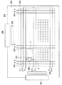
<TFT基板の全体構成>
まず、TFT基板の全体構成について説明する。図1は、TFT基板の全体構成を模式的に説明する平面図であり、LCD用のTFT基板を例にとって示している。
<Overall configuration of TFT substrate>
First, the overall configuration of the TFT substrate will be described. FIG. 1 is a plan view schematically illustrating the entire configuration of a TFT substrate, and shows an example of a TFT TFT substrate.
TFT基板200は、TFT201を有する画素204がマトリックス状に配列される表示領域202と、表示領域202の外側を囲む額縁領域203とに大きく分けられる。
The
表示領域202には、複数のゲート配線(走査信号線)3および複数のソース配線(表示信号線)9が配設される。複数のゲート配線3は互いに平行に配設され、複数のソース配線9も互いに平行に配設される。複数のゲート配線3と複数のソース配線9は直交する。図1では、ゲート配線3が横方向(X方向)に延在し、ソース配線9が縦方向(Y方向)に延在している。隣接するゲート配線3と隣接するソース配線9で囲まれた領域が画素204となるので、表示領域202には、画素204がマトリックス状に配列されることになる。
In the
図1では、代表的に1つの画素204を拡大して示している。画素204内には、少なくとも1つのTFT201が配設されている。TFT201は、ソース配線9とゲート配線3の交差点近傍に配置され、ゲート配線3に接続されるゲート電極と、ソース配線9に接続されるソース電極と、画素電極11に接続されるドレイン電極とを有している。また、画素電極11は補助容量電極5との間に補助容量209を形成しており、補助容量電極5は所定の共通電位が供給される補助容量配線210に接続されている。補助容量配線210は、ゲート配線3に平行に(ソース配線9に直交するように)延在し、ゲート配線3と補助容量配線210とは交互に配設される。
In FIG. 1, one
一方、TFT基板200の額縁領域203には、走査信号駆動回路205および表示信号駆動回路206が設けられている。図示は省略するが、ゲート配線3は、表示領域202から走査信号駆動回路205が設けられた側の額縁領域203へと引き出され、走査信号駆動回路205に接続されている。同様に、ソース配線9は、表示領域202から表示信号駆動回路206が設けられた側の額縁領域203へと引き出され、表示信号駆動回路206に接続されている。
On the other hand, a scanning
走査信号駆動回路205の近傍には、走査信号駆動回路205を外部と接続させるための接続基板207が配設され、表示信号駆動回路206の近傍には、表示信号駆動回路206を外部と接続させるための接続基板208が配設されている。これら接続基板207および208は、例えば、FPC(Flexible Printed Circuit)などの配線基板である。
A
走査信号駆動回路205には、接続基板207を介して外部から各種の制御信号が供給され、表示信号駆動回路206には、接続基板208を介して外部から各種の制御信号および画像データが供給される。走査信号駆動回路205は、外部からの制御信号に基づいて、ゲート配線3にゲート信号(走査信号)を供給する。このゲート信号によって、ゲート配線3が一定周期で順番に選択される。表示信号駆動回路206は、外部からの制御信号に基づいて、画像データに応じた表示信号をソース配線9に供給する。この走査信号駆動回路205と表示信号駆動回路206の動作によって、表示信号に応じた表示電圧が各画素204に供給される。
Various control signals are supplied to the scanning
本発明に係る薄膜トランジスタは、画素204に設けられるTFT201に適用可能なことはもちろん、走査信号駆動回路205および表示信号駆動回路206を構成するスイッチング素子としても好適に用いることができる。なお、走査信号駆動回路205および表示信号駆動回路206は、TFT基板200上に形成されるとは限らず、例えば、TCP(Tape Carrier Package)を用いて構成され、TFT基板200に接続される場合もある。
The thin film transistor according to the present invention can be applied not only to the
また、補助容量電極5は、後述するように、画素電極11と平面視で重複(重畳)するように配設され、画素電極11を一方の電極、補助容量電極5をもう一方の電極とする補助容量209を形成する。各画素204の補助容量電極5は、補助容量配線210に接続されて結束し、例えば走査信号駆動回路205や表示信号駆動回路206などから所定の共通電位が供給される。
Further, as will be described later, the
TFT201は、画素電極11に表示電圧を供給するためのスイッチング素子として機能し、ゲート配線3からゲート電極に与えられるゲート信号により、オン/オフが制御される。TFT201がオンになると、ソース配線9からドレイン電極に供給された表示電圧が画素電極11に印加され、画素電極11と対向基板(不図示)の対向電極との間に、表示電圧に応じた電界が生じる。画素電極11と対向電極との間には液晶を介して補助容量209と並列な容量(液晶容量)が形成される。画素電極11に印加された表示電圧は、液晶容量と補助容量209によって一定期間保持される。
The
対向基板は、例えばカラーフィルタ基板であり、TFT基板200の前面側(視認側)に配置される。対向基板には、カラーフィルタ、ブラックマトリックス(BM)、対向電極および配向膜等が形成される。配向膜は、TFT基板200の表面にも形成されていてもよい。また、IPS(In Plane Switching)方式やFFS(Fringe Field Switching)方式の液晶表示装置の場合、対向電極は、対向基板ではなくTFT基板200上に配設される。
The counter substrate is, for example, a color filter substrate, and is disposed on the front side (viewing side) of the
TFT基板200と対向基板とが一定の間隙(セルギャップ)を介して貼り合わされ、その間隙に液晶が注入されて封止されることで、液晶表示パネルが形成される。すなわち、液晶表示パネルは、TFT基板200と対向基板との間に液晶層が挟持された構造となる。さらに、液晶表示パネルの外面には、偏光板、位相差板等が設けられる。また、液晶表示パネルの背面側(TFT基板200の裏側)には、バックライトユニット等が配設される。
The
<液晶表示装置の動作>
続いて、液晶表示装置の動作について説明する。TFT基板200と対向基板との間に教示されている液晶は、画素電極11と対向電極との間に生じる電界によって駆動される(配向方向が制御される)。液晶の配向方向が変化すると、それを通過する光の偏光状態が変化する。よって、偏光板を通過して直線偏光となったバックライトユニットからの光は、液晶表示パネルの液晶層を通過するときに偏光状態が変化する。具体的には、バックライトユニットからの光は、TFT基板200側の偏光板によって直線偏光になる。そして、この直線偏光が液晶層を通過することによって、その偏光状態が変化する。
<Operation of liquid crystal display device>
Next, the operation of the liquid crystal display device will be described. The liquid crystal taught between the
液晶層を通過した光は、その偏光状態により、対向基板側の偏光板を通過する光量が変化する。すなわち、バックライトユニットから液晶表示パネルを透過する透過光のうち、視認側の偏光板を通過する光の光量が変化する。液晶の配向方向は、画素電極11に印加されている表示電圧によって変化する。したがって、表示電圧を制御することによって、視認側の偏光板を通過する光量を制御できる。液晶表示装置では、画素ごとに印加する表示電圧を表示データに基づいて制御することで、所望の画像を表示させている。
The amount of light passing through the liquid crystal layer changes through the polarizing plate on the counter substrate side depending on the polarization state. That is, among the transmitted light that passes through the liquid crystal display panel from the backlight unit, the amount of light that passes through the viewing-side polarizing plate changes. The alignment direction of the liquid crystal changes depending on the display voltage applied to the
<TFT基板の画素の構成>
次に、図2および図3を参照して、本実施の形態に係るTFT基板200のより詳細な構成について説明する。以下では、TFT基板200は透過型の液晶表示装置に用いられるものとして説明する。
<TFT substrate pixel configuration>
Next, a more detailed configuration of the
図2は、画素204を含むTFT基板200の主要部の平面構成を示す図であり、図3は、その断面構成を示す図である。図3では、図2に示すX−X線、Y−Y線およびZ−Z線に対応する断面に対応している。X−X線に沿った断面は、画素204の形成領域(以下「画素部」)に対応する。Y−Y線に沿った断面は、ゲート配線3にゲート信号を供給するためのゲート端子4およびゲート端子パッド18の形成領域(以下「ゲート端子部」)に対応する。Z−Z線に沿った断面は、ソース配線9に表示信号を印加するためのソース端子10およびソース端子パッド19の形成領域(以下「ソース端子部」)に対応する。
FIG. 2 is a diagram showing a planar configuration of the main part of the
さらに、X−X線に沿った画素部の断面は、図3に示すように、ゲート配線3とソース配線9とが交差する領域である「ゲート・ソース配線交差部」と、TFT201の形成領域である「TFT部」と、画素電極11をTFT201のドレインに接続させるコンタクトの形成領域である「ドレインコンタクト部」と、画素電極11の形成領域である「画素電極部」と、補助容量209の形成領域である「補助容量部」とを含んでいる。
Further, as shown in FIG. 3, the cross section of the pixel portion along the line XX is a region where the
図3に示すように、TFT基板200は、例えばガラス等の透明性絶縁基板である基板1を用いて形成される。基板1上には、同じ導電膜(第1の導電膜)が選択的に配設されて、各種の配線や電極を構成している。すなわち、ゲート端子部にはゲート端子4が配設され、ゲート・ソース配線交差部にはゲート配線3が配設され、TFT部にはゲート電極2が配設され、補助容量部には補助容量電極5が配設されている。そして、これらを覆うように、絶縁膜6が配設されている。絶縁膜6は、TFT部ではゲート絶縁膜として機能するため、以下では「ゲート絶縁膜」と称する。
As shown in FIG. 3, the
TFT部のゲート絶縁膜6上には、下層の第1の半導体層12aおよび上層の第2の半導体層12bとが積層して成る2層構造の半導体膜12(チャネル層)が形成されている。
On the
また、ゲート絶縁膜6および半導体膜12上には、同じ導電膜(第2の導電膜)が選択的に配設されて、各種の配線や電極を構成している。
Further, the same conductive film (second conductive film) is selectively provided on the
例えばTFT部には、第2の半導体層12b上に接合されたソース電極7およびドレイン電極8が互いに離間して配設されている。ソース電極7とドレイン電極8との間の半導体膜12では、第2の半導体層12bが除去されて、第1の半導体層12aの表面が露出している。その露出した第1の半導体層12aの部分が、TFT201のチャネルが形成されるチャネル領域13(バックチャネル)となる。
For example, in the TFT portion, a
チャネル領域13では、ソース電極7およびドレイン電極8と半導体膜12との接合端部において、第2の半導体層12bの端部が、ソース電極7およびドレイン電極8の端部よりも後退している。つまり、断面視で、ソース電極7およびドレイン電極の端部は、第2の半導体層12bよりも突出した庇形状となっている。
In the
本実施の形態では、半導体膜12を構成する第1および第2の半導体層12a,12bは、酸化物半導体で構成される。ここでいう酸化物半導体とは、導電率が10−7〜10S/cmであるもの、あるいはキャリア濃度が1011〜1018個/cm3の範囲にあるものとする。導電率が10S/cmよりも大きい場合や、キャリア濃度が1018個/cm3よりも大きい場合は、電気が常時流れやすくなり、半導体膜としてのスイッチングの機能を示さない場合があるからである。導電率が10−5〜10−1S/cmの範囲内、あるいは、キャリア濃度が1012〜1017個/cm3の範囲内であれば、より好ましい。
In the present embodiment, the first and second semiconductor layers 12a and 12b constituting the
酸化物半導体を半導体膜12(チャネル層)に用いることで、アモルファスシリコンを用いる場合よりも高い移動度有するTFT201を実現することができる。
By using an oxide semiconductor for the semiconductor film 12 (channel layer), the
具体的には、第1の半導体層12aとして、例えば酸化亜鉛(ZnO)に酸化インジウム(In2O3)、および酸化すず(SnO2)を添加したIn−Zn−Sn−O系の酸化物半導体を用いることができる。また、第2の半導体層12bとしては、酸化亜鉛(ZnO)に酸化ガリウム(Ga2O3)、酸化インジウム(In2O3)を添加したIn−Ga−Zn−O系の酸化物半導体を用いることができる。第1および第2の半導体層12a,12bの両方を酸化物半導体とすることで、それらを積層させてもその界面で還元反応は生じず、当該界面にダメージ層が形成されることはない。
Specifically, as the
第1および第2の半導体層12a,12bの材料として例示した、In−Zn−Sn−O系の酸化物半導体およびIn−Ga−Zn−O系の酸化物半導体は、いずれもシュウ酸などのカルボン酸を含むエッチング薬液に可溶であり、それを用いてエッチング加工が可能である。 The In—Zn—Sn—O-based oxide semiconductor and the In—Ga—Zn—O-based oxide semiconductor exemplified as the materials of the first and second semiconductor layers 12a and 12b are both oxalic acid and the like. It is soluble in an etchant containing carboxylic acid and can be etched using it.
一方、Al、Mo、AgおよびCu系の電極材料として一般的に用いられる金属膜のエッチング薬液として知られている、リン酸を含む薬液、例えばリン酸と硝酸と酢酸の混酸(Phosphoric acid、Acetic acid、Nitric acid:以下「PAN」)薬液に対しては、前者のIn−Zn−Sn−O系の酸化物半導体は、広い組成範囲で不溶もしくは難溶性を有し、それを用いてエッチング加工をすることができない。それに対して、後者のIn−Ga−Zn−O系の酸化物半導体は、リン酸を含む薬液に対し、広い組成範囲で可溶性を有し、それを用いてエッチング加工(除去)することができる。 On the other hand, a chemical solution containing phosphoric acid, for example, a mixed acid of phosphoric acid, nitric acid and acetic acid (Phosphoric acid, Acetic, known as an etching chemical solution for metal films generally used as Al, Mo, Ag, and Cu-based electrode materials. acid, Nitric acid (hereinafter “PAN”) For chemical solutions, the former In—Zn—Sn—O-based oxide semiconductors are insoluble or sparingly soluble in a wide composition range, and are used for etching. I can't. On the other hand, the latter In—Ga—Zn—O-based oxide semiconductor is soluble in a chemical composition containing phosphoric acid in a wide composition range, and can be etched (removed) using it. .
さらに、両者は、Cr系金属膜のエッチング薬液として知られる硝酸第二セリウムアンモニウムを含む薬液(Cerium Ammonium Nitrate:以下「CAN」)に対しても、PAN薬液と同様の特性を示す。 Furthermore, both exhibit the same characteristics as the PAN chemical solution with respect to a chemical solution containing ceric ammonium nitrate (hereinafter referred to as “CAN”), which is known as an etching chemical solution for Cr-based metal films.
図3に戻り、ソース端子部には、ゲート絶縁膜6の上に、ソース電極7およびソース配線9と同じ導電膜(第2導電膜)で形成されたソース端子10が配設されている。ソース端子10は、ソース電極7に接続するソース配線9の端部に形成される。
Returning to FIG. 3, a
基板1の全体を覆うように、保護絶縁膜14が形成されている。保護絶縁膜14には、複数のコンタクトホールが形成されている。
A protective insulating
例えば、ドレインコンタクト部には、ドレイン電極8に達するコンタクトホール15(以下「ドレインコンタクトホール」)が形成される。画素電極部の保護絶縁膜14上には、画素電極11が配設されるが、この画素電極11は、ドレインコンタクトホール15を介してドレイン電極8と接触して電気的に接続されている。さらに、画素電極11は、補助容量部に形成されている補助容量電極5の上方にまで延在し、画素電極11と補助容量電極5とによって補助容量209(図1)が形成される。なお、本実施の形態のTFT基板200は、透過型の液晶表示装置に用いられるので、画素電極11は透光性導電膜を用いて形成される。
For example, a
一方、ゲート端子部には、保護絶縁膜14およびゲート絶縁膜6を貫通してゲート端子4に達するコンタクトホール16が形成されている(以下「ゲート端子コンタクトホール」)。ゲート端子部の保護絶縁膜14上には、ゲート端子コンタクトホール16を介してゲート端子4の表面と接触し電気的に接続されるゲート端子パッド18が、画素電極11と同じ透光性導電膜を用いて形成される。
On the other hand, a
また、ソース端子部には、保護絶縁膜14を貫通してソース端子10に達するコンタクトホール17(以下「ソース端子コンタクトホール」)が形成されている。ソース端子部の保護絶縁膜14上には、ソース端子コンタクトホール17を介してソース端子10の表面と接触し電気的に接続されるソース端子パッド19が、画素電極11と同じ透光性導電膜を用いて配設される。
Further, a contact hole 17 (hereinafter referred to as “source terminal contact hole”) that penetrates the protective insulating
次に、画素204の平面構成について説明する。図2に示すように、複数のゲート配線3は、複数のソース配線9と直交するように横方向(X方向)に延在し、互いに平行して配設されている。また、ゲート配線3は、TFT201のゲート電極2と一体的に形成されている。すなわち、ゲート配線3におけるTFT201形成領域(TFT部)の部分が、ゲート電極2となっている。ゲート配線3において、ゲート電極2となる部分は他の部分よりも幅広に形成されている。
Next, a planar configuration of the
ゲート電極2の上には、ゲート絶縁膜4(図3)を介して、半導体膜12が形成されており、さらにその上にソース電極7およびドレイン電極8が設けられる。ソース電極7とドレイン電極8は、ゲート電極2の上方で互いに離間して対向配置され、その間に露出した半導体膜12の部分がTFT201のチャネル領域13となる。なお、半導体膜12のパターンは、平面視で、ゲート電極2のパターンの内側に入るように(ゲート電極2の外側にはみ出さないように)構成されている。
A
ゲート配線3の一方の端部はゲート端子4に接続される。上記したように、ゲート端子4の上には、ゲート端子コンタクトホール16介してゲート端子4に接続するゲート端子パッド18が形成されている。なお、ゲート端子パッド18は、走査信号駆動回路205(図1)に接続され、ゲート配線3に供給するゲート信号(走査信号)が印加される。
One end of the
縦方向(Y方向)に延在するソース配線9は、ゲート配線3との交点近傍で分岐しており、その分岐した部分がTFT201の形成領域まで延びてソース電極7を構成する。ソース電極7は、ゲート電極2の上方に重畳するように配置される。
The
ソース配線9の一方の端部はソース端子10に接続されている。上記したように、ソース端子10の上には、ソース端子コンタクトホール17を介してソース端子10に接続するソース端子パッド19が形成されている。なお、ソース端子パッド25は、表示信号駆動回路206(図1)に接続され、ソース配線9に供給する表示信号が印加される。
One end of the
画素電極11は、ドレインコンタクトホール15を介してドレイン電極8と電気的に接続される。さらに、画素電極11の一部はゲート絶縁膜6および保護絶縁膜14(図3)を介して補助容量電極5と一部が重畳しており、その重畳部分で補助容量209(図1)が形成される。
The
補助容量電極5は、画素電極11の端縁部と重複するように、平面視でΠ(パイ)字状に形成されている。補助容量電極5の形状はΠ字状に限らず、画素電極11との間で所望の容量値が得られれば、任意の形状(例えば直線状やL字状)でよい。
The
<製造方法>
本実施の形態に係るTFT基板200の製造方法について、図4〜図7を参照しつつ説明する。なお、図4〜図7においては、図3に示した要素に対応する要素には、それと同一符号を付してある。
<Manufacturing method>
A method for manufacturing the
まず、基板1を洗浄液または純水を用いて洗浄する。本実施の形態では、厚さ0.5mmの無アルカリガラス基板を基板1として用いる。そして、洗浄された基板1の一方の主面全面に、ゲート電極2、ゲート配線3などを構成する第1の導電膜を成膜する。
First, the
第1の導電膜としては、例えばアルミニウム(Al)、クロム(Cr)、銅(Cu)、モリブデン(Mo)やこれらに他の元素を微量に添加した合金等を用いることができる。また、これらの金属または合金を2層以上含む積層構造としてもよい。これらの金属、合金を用いることによって、比抵抗値が50μΩcm以下(導電率が2×10⁴S/cm以上)の低抵抗な導電膜を得ることができる。 As the first conductive film, for example, aluminum (Al), chromium (Cr), copper (Cu), molybdenum (Mo), an alloy in which a small amount of other elements is added, or the like can be used. Moreover, it is good also as a laminated structure containing two or more layers of these metals or alloys. By using these metals and alloys, a low-resistance conductive film having a specific resistance value of 50 μΩcm or less (conductivity of 2 × 10 4 S / cm or more) can be obtained.
本実施の形態では、第1の導電膜としてMo膜を用い、Arガスを用いたスパッタリング法でMo膜を200nmの厚さに成膜した。その後、Mo膜上にレジスト材を塗布し、写真製版工程(第1回目)でフォトレジストパターンを形成し、当該フォトレジストパターンをエッチングマスクとして、Mo膜をエッチングによりパターニングする。その後、フォトレジストパターンを除去する。その結果、図4に示すように、基板1上に、ゲート電極2、ゲート配線3、ゲート端子4および補助容量電極5が形成される。
In this embodiment mode, a Mo film is used as the first conductive film, and the Mo film is formed to a thickness of 200 nm by a sputtering method using Ar gas. Thereafter, a resist material is applied onto the Mo film, a photoresist pattern is formed in the photolithography process (first time), and the Mo film is patterned by etching using the photoresist pattern as an etching mask. Thereafter, the photoresist pattern is removed. As a result, as shown in FIG. 4, the
第1の導電膜のエッチングプロセスでは、リン酸、酢酸および硝酸を含む溶液(PAN薬液)によるウエットエッチングを用いることができる。PAN薬液としては、リン酸が40〜93wt%(重量%)、酢酸が1〜40wt%、硝酸が0.5〜15wt%の範囲のものが好ましい。本実施の形態においては、リン酸70wt%+酢酸7wt%+硝酸5wt%+水のPAN薬液を用い、液温を25℃に設定して、Mo膜をエッチングした。
In the etching process of the first conductive film, wet etching using a solution (PAN chemical solution) containing phosphoric acid, acetic acid, and nitric acid can be used. As the PAN chemical, phosphoric acid is preferably in the range of 40 to 93 wt% (wt%), acetic acid in the range of 1 to 40 wt%, and nitric acid in the range of 0.5 to 15 wt%. In the present embodiment, the Mo film was etched using a PAN chemical solution of phosphoric acid 70 wt% +
次に、図5に示す工程において、基板1の一方の主面全面に、ゲート端子4、ゲート配線3、ゲート電極2および補助容量電極5を覆うようにゲート絶縁膜6を成膜する。ゲート絶縁膜6は、化学的気相成長(CVD)法を用いて、酸化シリコン(SiO)膜を形成することで得られる。本実施の形態では、厚さ300nmの酸化シリコン膜を、約300℃の基板加熱条件下で成膜した。なお、酸化シリコン膜は、水分(H2O)や水素(H2)あるいはナトリウム(Na)やカリウム(K)のようなTFT特性に影響を及ぼす不純物元素に対するバリア性(遮断性)が弱いことから、ゲート絶縁膜6は、酸化シリコン膜の下層に例えばバリア性に優れる窒化シリコン(SiN)膜などを設けた積層構造としてもよい。
Next, in the step shown in FIG. 5, a
さらに、ゲート絶縁膜6の上に、半導体膜12を構成する酸化膜半導体である第1の半導体層12aおよび第2の半導体層12bをこの順に成膜し、下層が第1の半導体層12a、上層が第2の半導体層12bとなる積層膜を形成する。
Further, a
第1の半導体層12aとしては、この後のソース電極およびドレイン電極を形成するための第2の導電膜のエッチングプロセスに対して耐性を有する酸化物材料を用いる。例えば酸化亜鉛(ZnO)に酸化インジウム(In2O3)、および酸化すず(SnO2)を添加したIn−Zn−Sn−O系の酸化物を用いることができる。
As the
なお、本明細書において、「ソース電極およびドレイン電極のエッチングプロセスに対して耐性を有する」とは、導電膜を加工してソース電極およびドレイン電極を形成する一連のエッチングプロセス中に暴露されても、少なくとも消失せずに残存可能であることと定義される(ただし、半導体膜を半導体として充分に機能させるためには、最初の膜厚の半分以上が残っていることが好ましい)。 In this specification, “resistant to the etching process of the source electrode and the drain electrode” means that it is exposed during a series of etching processes in which the conductive film is processed to form the source electrode and the drain electrode. Is defined as being able to remain at least without disappearing (however, in order to sufficiently function the semiconductor film as a semiconductor, it is preferable that more than half of the initial film thickness remain).
本実施の形態では、In:Zn:Sn:Oの原子組成比が2:6:2:13であるIn−Zn−Sn−Oターゲット[In2O3・(ZnO)6・(SnO2)2]を用いたスパッタリング法により、第1の半導体層12aを成膜した。このとき、ArガスやKrガスを用いてスパッタリングすると、通常は、酸素の原子組成比が化学量論組成よりも少ない酸素イオン欠乏状態(上記の例ではOの組成比が13未満)の酸化膜が形成されるため、好ましくない。したがって、Arガスに酸素(O2)ガスを混合させてスパッタリングすることが望ましい。ここでは、Arガスに対して分圧比で10%のO2ガスを添加した混合ガスを用いてスパッタリングを行い、In−Zn−Sn−O膜を40nmの厚さで成膜する。
In this embodiment mode, an In—Zn—Sn—O target [In 2 O 3. (ZnO) 6. (SnO 2 ) in which the atomic composition ratio of In: Zn: Sn: O is 2: 6: 2: 13 is used. 2 ] was used to form a
成膜直後のIn−Zn−Sn−O膜は非晶質構造であり、シュウ酸を含む薬液に可溶性を示すため、それを用いたエッチング加工が可能である。一方で、上記のPAN系薬液およびCAN系薬液では、液温20℃から40℃の範囲で5分間浸漬した後でも膜減りはほとんど認められず、難溶性を示すことから、エッチング加工は不可能である。 The In—Zn—Sn—O film immediately after film formation has an amorphous structure and is soluble in a chemical solution containing oxalic acid; therefore, etching using the film can be performed. On the other hand, with the above-mentioned PAN-based chemicals and CAN-based chemicals, etching is impossible because almost no film loss is observed even after immersion for 5 minutes in the range of 20 ° C to 40 ° C. It is.
一方、第2の半導体層12bとしては、この後のソース電極およびドレイン電極を形成するための第2の導電膜のエッチングプロセスに対してエッチング性を有する酸化物材料を用いる。例えば酸化亜鉛(ZnO)に酸化ガリウム(Ga2O3)、酸化インジウム(In2O3)を添加したIn−Ga−Zn−O系の酸化物を用いることができる。
On the other hand, as the
なお、本明細書において、「ソース電極およびドレイン電極のエッチングプロセスに対してエッチング性を有する」とは、導電膜を加工してソース電極およびドレイン電極を形成する一連のエッチングプロセス中に暴露させると、完全に除去可能であることと定義される。 Note that in this specification, “having etching property with respect to the etching process of the source electrode and the drain electrode” means that the conductive film is exposed during a series of etching processes for forming the source electrode and the drain electrode. , Defined as being completely removable.
本実施の形態では、In:Ga:Zn:Oの原子組成比が1:1:1:4であるIn−Ga−Zn−Oターゲット[In2O3・Ga2O3・(ZnO)2]を用いたスパッタリング法により、第2の半導体層12bを成膜した。このときも、ArガスやKrガスを用いてスパッタリングすると、通常は、酸素イオン欠乏状態(上記の例ではOの組成比が4未満)の酸化膜が形成されるため、好ましくない。したがって、Arガスに対して分圧比で10%のO2ガスを添加した混合ガスを用いてスパッタリングを行い、In−Ga−Zn−O膜を20nmの厚さで成膜する。
In this embodiment, an In—Ga—Zn—O target [In 2 O 3 .Ga 2 O 3. (ZnO) 2 having an atomic composition ratio of In: Ga: Zn: O of 1: 1: 1: 4 is used. The
成膜直後のIn−Ga−Zn−O膜は非晶質構造であり、シュウ酸を含む薬液に可溶性を示すため、それを用いたエッチング加工か可能である。またPAN系薬液およびCAN系薬液でも、シュウ酸を含む薬液の場合と同様に可溶性を示し、エッチング加工をすることが可能である。 The In—Ga—Zn—O film immediately after film formation has an amorphous structure and is soluble in a chemical solution containing oxalic acid; therefore, etching using the same can be performed. Also, PAN-based chemical solutions and CAN-based chemical solutions are soluble and can be etched as in the case of chemical solutions containing oxalic acid.
なお、本明細書における酸化物半導体の「非晶質構造」とは、具体的には、X線回折法による回折パターンにおいて、ハロー状のパターンが観測されるとともに、特定の結晶面による回折ピークが明確には観測されない結果が得られるものと定義する。すなわち非晶質中に結晶領域が存在したとしても、微結晶のためにX線回折では明確な回折ピークを示さないものも非晶質状態に含むものとする。 Note that the “amorphous structure” of an oxide semiconductor in this specification refers specifically to a diffraction pattern obtained by an X-ray diffraction method in which a halo-like pattern is observed and a diffraction peak due to a specific crystal plane is observed. Is defined as a result that is not clearly observed. That is, even if a crystal region exists in an amorphous state, those that do not show a clear diffraction peak in X-ray diffraction due to microcrystals are included in the amorphous state.
第1および第2の半導体層12a,12bを成膜した後、その上にレジスト材を塗布し、写真製版工程(第2回目)でフォトレジストパターンを形成し、当該フォトレジストパターンをエッチングマスクとして、第1および第2の半導体層12a,12bをエッチングによりパターニングする。その後、フォトレジストパターンを除去する。その結果、図5のように、TFT部のゲート絶縁膜6上に、チャネル層としての半導体膜12が形成される。
After the first and second semiconductor layers 12a and 12b are formed, a resist material is applied thereon, a photoresist pattern is formed in the photolithography process (second time), and the photoresist pattern is used as an etching mask. The first and second semiconductor layers 12a and 12b are patterned by etching. Thereafter, the photoresist pattern is removed. As a result, a
このエッチングプロセスでは、カルボン酸を含む薬液によるウエットエッチングを用いることができる。カルボン酸を含む薬液としては、シュウ酸を1〜10wt%の範囲で含むものが好ましい。本実施の形態では、シュウ酸5wt%+水のシュウ酸系薬液を用い、液温を25℃に設定して、第1および第2の半導体層12a,12bを同時に一括エッチングして半導体膜12を形成した。
In this etching process, wet etching using a chemical solution containing carboxylic acid can be used. As the chemical solution containing carboxylic acid, one containing oxalic acid in the range of 1 to 10 wt% is preferable. In the present embodiment, an oxalic acid chemical solution of 5 wt% oxalic acid + water is used, the temperature of the solution is set to 25 ° C., and the first and second semiconductor layers 12a and 12b are simultaneously etched simultaneously to form the
なお、半導体膜12のパターンは、図2にも示したように、平面視でゲート電極2のパターンよりも外側にはみ出さず、全体がゲート電極2の内側に入るように構成されている。この構成では、TFT基板1の裏面からバックライト光を照射して表示を行う透過型LCDにおいて、ゲート電極12パターンが遮光マスクとなって半導体膜12に光が直接入射することを防ぐことができ、光照射によるTFT特性の劣化を防止できる。
As shown in FIG. 2, the pattern of the
次に、図6に示す工程では、第2の導電膜を用いてソース電極7、ドレイン電極8、ソース配線9、ソース端子10を形成すると共に、ソース電極7とドレイン電極8の間の領域にTFT201のチャネル領域13を露出させる。
Next, in the step shown in FIG. 6, the
第2の導電膜としては、例えばアルミニウム(Al)、クロム(Cr)、銅(Cu)、モリブデン(Mo)やこれらに他の元素を微量に添加した合金等を用いることができる。また、これらの金属または合金を2層以上含む積層構造としてもよい。これらの金属、合金を用いることによって、比抵抗値が50μΩcm以下(導電率が2×10⁴S/cm以上)の低抵抗な導電膜を得ることができる。 As the second conductive film, for example, aluminum (Al), chromium (Cr), copper (Cu), molybdenum (Mo), an alloy in which a small amount of other elements is added, or the like can be used. Moreover, it is good also as a laminated structure containing two or more layers of these metals or alloys. By using these metals and alloys, a low-resistance conductive film having a specific resistance value of 50 μΩcm or less (conductivity of 2 × 10 4 S / cm or more) can be obtained.
本実施の形態では、第2の導電膜としてMo膜を用い、Arガスを用いたスパッタリング法でMo膜を200nmの厚さに成膜した。その後、Mo膜上にレジスト材を塗布し、写真製版工程(第3回目)でフォトレジストパターンを形成し、当該フォトレジストパターンをエッチングマスクとして、Mo膜をエッチングによりパターニングする。その後、フォトレジストパターンを除去する。その結果、図6に示すように、ソース電極8、ドレイン電極9、ソース配線9、ソース端子10およびTFTのチャネル領域13が形成される。
In this embodiment, a Mo film is used as the second conductive film, and the Mo film is formed to a thickness of 200 nm by a sputtering method using Ar gas. Thereafter, a resist material is applied onto the Mo film, a photoresist pattern is formed in the photolithography process (third time), and the Mo film is patterned by etching using the photoresist pattern as an etching mask. Thereafter, the photoresist pattern is removed. As a result, as shown in FIG. 6, the
上記の第2の導電膜のエッチングでは、ソース電極7とドレイン電極8が分離され、その間に半導体膜12が露出する。半導体膜12の上層部である第2の半導体層12bは、ソース電極7およびドレイン電極8のエッチングプロセスに対してエッチング性を有するので、露出した第2の半導体層12bの部分は除去される。一方、半導体膜12の下層部である第1の半導体層12aは、ソース電極7およびドレイン電極8のエッチングプロセスに対して耐性を有するので、除去されずに残り、その部分がチャネル領域13となる。る。つまり、チャネル領域13は、第1の半導体層12aにより構成されることになる。
In the etching of the second conductive film, the
第1および第2の半導体層12a,12bは、共に酸化物系なので両者の界面で還元反応は生じない。したがって、露出した第1の半導体層12aの表面(チャネル領域13の表面)には還元反応による酸素欠乏領域やダメージ層はほとんど存在しない。
Since the first and second semiconductor layers 12a and 12b are both oxide-based, no reduction reaction occurs at the interface between them. Therefore, the exposed surface of the
第2の導電膜のエッチングプロセスでは、リン酸、酢酸および硝酸を含む溶液(PAN薬液)によるウエットエッチングを用いることができる。ここでは、リン酸70wt%+酢酸7wt%+硝酸5wt%+水のPAN薬液を用いて液温を25℃に設定してMo膜をエッチングした。
In the etching process of the second conductive film, wet etching using a solution (PAN chemical solution) containing phosphoric acid, acetic acid, and nitric acid can be used. Here, the Mo film was etched by setting the liquid temperature to 25 ° C. using a PAN chemical solution of phosphoric acid 70 wt% +
このエッチングプロセスでは、まず第2の導電膜が除去され、それにより露出した第2の半導体層12bがさらに除去される。しかし、第2の半導体層12bが除去されて露出した第1の半導体層12aは、PAN薬液にほとんど溶けないため除去されずに残り、上でも述べたようにその部分がチャネル領域13となる。
In this etching process, first, the second conductive film is removed, and thereby the exposed
本実施の形態では、PAN薬液に対する第2の半導体層12bのエッチング速さが、同じくPAN薬液に対する第2の導電膜のエッチング速さよりも、速くなるように構成されている。そうすることにより、ソース電極7およびドレイン電極8のチャネル領域13側の端部において、平面視で、第2の半導体層12bの端部がソース電極7およびドレイン電極8の端部よりも後退する。また、断面視では、図6のようにソース電極7およびドレイン電極8の端部が第2の半導体層12bの端部よりも水平方向に突出して庇形状になる。
In the present embodiment, the etching rate of the
次に、図7に示す工程において、ソース電極7、ドレイン電極8、ソース配線9、ソース端子10、およびTFT201のチャネル領域13を覆うように、保護絶縁膜14を成膜し、保護絶縁膜14およびゲート絶縁膜6を貫通するドレインコンタクトホール15、ゲート端子コンタクトホール16およびソース端子コンタクトホール17を形成する。
Next, in the process illustrated in FIG. 7, the protective insulating
本実施の形態では、CVD法を用いて約250℃の基板加熱条件下で厚さ300nmの酸化シリコン(SiO)膜を成膜することで、保護絶縁膜14を形成した。そして、保護絶縁膜14上にレジスト材を塗布し、写真製版工程(第4回目)でフォトレジストパターンを形成し、当該フォトレジストパターンをエッチングマスクとして、保護絶縁膜14をエッチングすることで、ドレインコンタクトホール15、ゲート端子コンタクトホール16およびソース端子コンタクトホール17を形成した。
In this embodiment mode, the protective insulating
このエッチング工程では、フッ素系ガスを用いたドライエッチング法を用いることができる。この手法を用いることで、保護絶縁膜14を貫通するドレインコンタクトホール15およびソース端子コンタクトホール17と、保護絶縁膜14およびゲート絶縁膜6を貫通するゲート端子コンタクトホール16とを同時に形成できる。図7に示すように、ドレインコンタクトホール15はドレイン電極8に、ゲート端子コンタクトホール16はゲート端子4に、ソース端子コンタクトホール17はソース端子10に、それぞれ達するように形成される。
In this etching step, a dry etching method using a fluorine-based gas can be used. By using this technique, the
なお、酸化シリコン膜は、水分(H2O)や水素(H2)あるいはナトリウム(Na)やカリウム(K)のようなTFT特性に影響を及ぼす不純物元素に対するバリア性(遮断性)が弱いことから、保護絶縁膜14は、酸化シリコン膜の上層に例えばバリア性に優れる窒化シリコン(SiN)膜などを設けた積層構造としてもよい。このような積層構造の場合でも、フッ素ガスを用いたドライエッチング法を用いてコンタクトホールを形成することができる。
Note that a silicon oxide film has a weak barrier property (blocking property) against impurity elements that affect TFT characteristics such as moisture (H 2 O), hydrogen (H 2), sodium (Na), and potassium (K). The protective
次に、第3の導電膜(透光性導電膜)を用いて、画素電極11、ゲート端子パッド18およびソース端子パッド19を形成することで、図3に示した構成を完成させる。
Next, the
画素電極11は、ドレインコンタクトホール15を介してドレイン電極8と電気的に接続されるように形成する。また、画素電極11は、補助容量電極5との間で補助容量209が形成されるように、その一部がゲート絶縁膜6および保護絶縁膜14を介して補助容量電極5と重畳するように形成される。
The
ゲート端子パッド18およびソース端子パッド19は、ゲート端子コンタクトホール16およびソース端子コンタクトホール17を介して、それぞれゲート端子4およびソース端子10の表面と接触して電気的に接続されるように形成される。
The
本実施の形態では、第3の導電膜である透光性導電膜は、導電性酸化物であるIn−Zn−O膜(酸化インジウムIn2O3と酸化亜鉛ZnOとの混合比は、例えば90:10重量%)を用いた。ここでは、スパッタリング法を用いて、厚さ100nmのIn−Zn−O膜を成膜した。 In this embodiment, the light-transmitting conductive film that is the third conductive film is formed using an In—Zn—O film that is a conductive oxide (the mixing ratio of indium oxide In 2 O 3 and zinc oxide ZnO is, for example, 90: 10% by weight). Here, an In—Zn—O film with a thickness of 100 nm was formed by a sputtering method.
そして、In−Zn−O膜上にレジスト材を塗布し、写真製版工程(第5回目)でフォトレジストパターンを形成し、当該フォトレジストパターンをエッチングマスクとして、In−Zn−O膜をエッチングによりパターニングする。その後、フォトレジストパターンを除去することで、図3に示したように、画素電極11、ゲート端子パッド18およびソース端子パッド19が形成される。このエッチングプロセスでは、シュウ酸薬液によるウエットエッチング法を用いることができる。
Then, a resist material is applied onto the In—Zn—O film, a photoresist pattern is formed in the photolithography process (fifth time), and the In—Zn—O film is etched by using the photoresist pattern as an etching mask. Pattern. Thereafter, by removing the photoresist pattern, the
第3の導電膜を透光性導電膜としたのは、バックライト光を透過して表示を行う透過型LCDでは透光性の画素電極が必要だからである。一方、本発明を、外光を反射して表示を行う反射型LCDに適用する場合は、光を反射するAlやAgのような金属膜を画素電極として形成すればよい。また、本発明を、反射と透過の両方を兼ね備えた半透過型LCDに適用する場合は、光反射性と透光性の両方を有する画素電極を形成すればよい。 The reason why the third conductive film is a light-transmitting conductive film is that a light-transmitting pixel electrode is required for a transmissive LCD that transmits backlight and performs display. On the other hand, when the present invention is applied to a reflective LCD that reflects external light and performs display, a metal film such as Al or Ag that reflects light may be formed as a pixel electrode. When the present invention is applied to a transflective LCD having both reflection and transmission, a pixel electrode having both light reflectivity and light transmissivity may be formed.
以上の5回の写真製版工程を経て、図3に示した、本実施の形態に係るTFT基板200が完成する。
Through the above five photoengraving steps, the
その後、完成したTFT基板200の表面に配向膜やスペーサを形成する。配向膜は、液晶を配列させるための膜であり、ポリイミド等で構成される。また、別途作成した、カラーフィルタや配向膜を備えた対向基板を、TFT基板200と貼り合わせる。このときスペーサによってTFT基板200と対向基板との間に隙間が形成される。その隙間に液晶を注入して封止することによって、液晶表示パネルが形成される。最後に、液晶表示パネルの外側に偏光板、位相差板およびバックライトユニット等を配設することによってTFT−LCDが完成する。
Thereafter, an alignment film and a spacer are formed on the surface of the completed
<効果>
以上説明したように、本実施の形態に係るTFT基板の製造方法においては、5回の写真製版工程で、半導体のチャネル層に酸化物半導体を用いた高移動度を有するTFT201を備えた、高性能なLCD用のTFT基板200を製造することができる。
<Effect>
As described above, in the manufacturing method of the TFT substrate according to the present embodiment, the
また、ソース電極7およびドレイン電極8のエッチング加工と、半導体膜12のチャネル領域13を形成するための第2の半導体層12bの除去とを、同じエッチングプロセスを用いて同時に行うようにしている。よって、工程数の増加を抑えつつ、生産性良く酸化物半導体膜を用いたTFT201を有するTFT基板200を製造することができる。なお、このエッチングプロセスは、薬液を用いたウエットエッチング法に限らず、エッチングガスを用いたドライエッチング法、あるいは、ウエットエッチング法とドライエッチング法とを組み合わせたものを用いてもよい。
Further, the etching process of the
本実施の形態に係るTFT基板200では、半導体膜12が、ソース電極7およびドレイン電極8のエッチングプロセス(薬液)に対して耐性を有する下層の第1の半導体層12aと、エッチング性を有する上層の第2の半導体層12bとを含む少なくとも2層構造から成っている。そのため、ソース電極7およびドレイン電極8が除去された半導体膜12のチャネル領域13は、第2の半導体層12bが除去され、第1の半導体層12aで形成された構成となる。
In the
ソース電極7およびドレイン電極8を構成する導電膜(第2の導電膜)との界面反応による還元層(酸素欠乏層)やダメージ層は第2の半導体層12bに形成されるが、チャネル領域13ではその第2の半導体層12bが除去されているため、TFT201のオフ電流値を低減させ、TFT201の特性(TFT特性)を向上させることができる。その結果、表示ムラやクロストークなどの表示不良を防止でき、高品質なLCD用のTFT基板200を得ることができる。
Although the reduction layer (oxygen-deficient layer) and the damage layer due to the interface reaction with the conductive film (second conductive film) constituting the
また、ソース電極7およびドレイン電極8におけるチャネル領域13側の端部において、平面視で、第2の半導体層12bの端部がソース電極7およびドレイン電極8の端部よりも後退し、断面視で、ソース電極7およびドレイン電極8の端部が第2の半導体層12bの端部よりも突出して庇状となっている。したがって、ソース電極7およびドレイン電極8の端部における電界集中を抑制して良好なTFT特性を得ることができる。特に深いゲート電極の負バイアスが印加されたときのドレイン電極8端部における電界集中を抑制できるので、オフ電流の増大(跳ね上がり)を抑制することができる。
In addition, at the end of the
さらに、半導体膜12のパターンは、図2に示すように、平面視で、ゲート電極2のパターンよりも外側にはみ出さず、全体がゲート電極2の内側に入るように構成されている。この場合、TFT基板2001の裏面からバックライト光を照射して表示を行う透過型もしくは半透過型のLCDにおいて、ゲート電極12のパターンが遮光マスクとなって半導体膜12に直接バックライト光が入射することを防ぐことができる。しかも、第2の半導体層12bがソース電極7およびドレイン電極8端部より後退し、ソース電極7およびドレイン電極8が庇構造となっているため、電界強度が大きくなるソース電極7およびドレイン電極8と第2の半導体層12bとの接合端部への、直接的な光照射がなくなる。これにより、酸化物半導体を用いたTFTで課題となる、光照射によるTFT特性の劣化や閾値の変動をさらに抑制することができる。
Further, as shown in FIG. 2, the pattern of the
<プロセスの変形例>
図5の工程において、酸化物半導体の半導体膜12を形成した後に、基板1を熱処理してもよい。本実施の形態では、第1の半導体層12aとして非晶質構造のIn−Zn−Sn−O膜を用い、第2の半導体層12bとして非晶質構造のIn−Ga−Zn−O膜を用いた。前者のIn−Zn−Sn−O膜は、その組成比にもよるが、250℃から300℃の熱処理で結晶化する(結晶化温度が250℃から300℃近傍にある)。一方、後者のIn−Ga−Zn−O膜は、結晶化温度が500℃以上で前者よりも高い。
<Modification of process>
In the step of FIG. 5, the
本実施の形態のように、第1の半導体層12aの結晶化温度T1と、第2の半導体層12bの結晶化温度T2とが、T1<T2の条件を満たす場合には、半導体膜12を形成した後に、T1以上、T2未満の温度で基板1を熱処理してもよい。そうすることにより、第1の半導体層12aであるIn−Zn−Sn−O膜は多結晶化し、第2の半導体層12bであるIn−Ga−Zn−O膜は依然として非晶質構造を保つ。多結晶化したIn−Zn−Sn−O膜は、PAN薬液に対する耐性が非晶質状態に比べて向上する。よって、図6の工程で、第2の導電膜と第2の半導体層12bを同時にエッチングしてチャネル領域13を形成する工程における、プロセスマージンが向上する。また、チャネル領域13の表面が、化学的に安定な多結晶化された酸化物半導体膜で形成されるので、閾値変動を抑制することができ、TFT特性の信頼性が向上するという効果も得られる。
When the crystallization temperature T1 of the
また、本実施の形態では、半導体膜12において、第1の半導体層12aの膜厚を40nm、第2の半導体層12bの膜厚を20nmとしたが、それらの厚さはこれに限られず、TFT特性や生産性などの点から任意に設定すればよい。ただし、第1の半導体層12aの膜厚は、第2の半導体層12bの膜厚よりも厚く設定することが好ましい。そうすることで、図6の工程において、チャネル領域13を形成するときのプロセスマージンが向上する。
In the present embodiment, in the
また、図6の工程の後、保護絶縁膜14を成膜する前に、基板1を酸素(O2)または水蒸気(H2O)を含む雰囲気下で熱処理を行ってもよい。熱処理は200℃以上400℃以下が好ましい。あるいは、UV(紫外線)光を照射したり、O2ガスやN2Oガスを用いてプラズマ処理を行ってもよい。それにより、チャネル領域13の表面の酸素欠乏状態や、原子配列の乱れなどを緩和することができるため、さらにTFT特性を向上させることができる。
In addition, after the process of FIG. 6 and before forming the protective insulating
<半導体膜の変形例>
本実施の形態では、下層の第1の半導体層12aとしてIn−Zn−Sn−O系の酸化物半導体を用い、上層の第2の半導体層12bとしてIn−Ga−Zn−O系の酸化物半導体を用いたが、それぞれ当該材料に限られるものではない。
<Modification of semiconductor film>
In this embodiment, an In—Zn—Sn—O-based oxide semiconductor is used as the lower
ボトムゲートのバックチャネル型TFTの場合において、第1の半導体層12aに求められる特性は、ソース電極7およびドレイン電極8のエッチングプロセスにおいて耐性を有すること、すなわちエッチングされないことである。本実施の形態のようにソース電極7およびドレイン電極8のエッチングプロセスをPAN系薬液またはCAN系薬液を用いたウエットエッチング法で実施する場合には、第1の半導体層12aとして、例えば他にもZn−Sn−O系、In−Al−Sn−O系、In−Si−Sn−O系、In−Al−Zn−Sn−O系のようなすず(Sn)を含む酸化物半導体膜を好適に用いることができる。
In the case of a bottom-gate back channel TFT, the characteristics required for the
このとき、Snの組成は半導体膜の特性に応じて任意に決めることができるが、酸化物半導体膜を構成する全金属元素に対するSnの原子比が0.05以上0.5以下であることが好ましい。例えば、Zn−Sn−O系の場合は、0.05≦Sn/(Zn+Sn)≦0.5、本実施の形態で用いたIn−Zn−Sn−O系の場合は、0.05≦Sn/(In+Zn+Sn)≦0.5とするとよい。Snを原子比で0.05以上含ませることによって、PAN系薬液およびCAN系薬液に対するエッチング耐性を持たせることができる。Snの原子比が0.5を超えると、一般的な酸化物半導体膜のエッチング薬液として知られている、カルボン酸を含む薬液に対するエッチング速さが低下するため、パターニング加工が困難になってしまう。 At this time, the composition of Sn can be arbitrarily determined according to the characteristics of the semiconductor film, but the atomic ratio of Sn to all metal elements included in the oxide semiconductor film is 0.05 or more and 0.5 or less. preferable. For example, in the case of the Zn—Sn—O system, 0.05 ≦ Sn / (Zn + Sn) ≦ 0.5, and in the case of the In—Zn—Sn—O system used in this embodiment, 0.05 ≦ Sn. /(In+Zn+Sn)≦0.5 is preferable. By including Sn in an atomic ratio of 0.05 or more, etching resistance to a PAN chemical solution and a CAN chemical solution can be provided. When the atomic ratio of Sn exceeds 0.5, the etching rate with respect to a chemical solution containing a carboxylic acid, which is known as a general chemical solution for oxide semiconductor film, decreases, and patterning becomes difficult. .
もちろん、Snを含まなくても、第1の半導体層12aに求められる特性を満たす材料であればよい。また酸化物半導体に限らず、他の化合物半導体、例えば、Al−NやGa−Nなどの窒化物半導体膜、または窒化物と酸化物とを組み合わせた化合物半導体膜を用いることも可能である。窒化物半導体膜を含むことによって、PAN系薬液およびCAN系薬液に対するエッチング耐性を持たせることができる。
Needless to say, a material satisfying the characteristics required for the
一方、第2の半導体層12bに求められる特性は、ソース電極7およびドレイン電極8のエッチングプロセスにおいて同時にエッチング加工(除去)できることである。本実施の形態のようにソース電極7およびドレイン電極8のエッチングプロセスを、PAN系薬液またはCAN系薬液を用いたウエットエッチング法で実施する場合には、第2の半導体層12bとして、例えば他にもIn−Zn−O系、In−Al−Zn−O系、In−Hf−Zn−O系、In−Zr−Zn−O系、In−Mg−Zn−O系、In−Y−Zn−O系のような酸化物半導体膜を用いることができる。
On the other hand, the characteristic required for the
特に、酸化物半導体膜にガリウム(Ga)、アルミニウム(Al)、ハフニウム(Hf)、ジルコニウム(Zr)あるいはイットリウム(Y)を添加した場合は、エネルギーバンドギャップEgを広げる効果がある。 In particular, when gallium (Ga), aluminum (Al), hafnium (Hf), zirconium (Zr), or yttrium (Y) is added to the oxide semiconductor film, there is an effect of widening the energy band gap Eg.
本実施の形態では、第2の半導体層12bのEg値が第1の半導体層12aのEg値よりも大きくなるように構成することが、ゲート電極に負バイアスを印加したときのオフ状態において、ドレイン側からのリーク電流を低減し、オフ電流値を低減する効果が得られるため好ましい。したがって、第2の半導体層12bは、Ga、Al、Hf、ZrまたはYのいずれかを含むか、またはこれらの元素の添加量が第1の半導体層12aよりも多い酸化物半導体を材料とすることが好ましい。
In this embodiment, the Eg value of the
<発明の他の適用例>
本発明に係るTFT基板は、液晶表示装置以外の表示装置に適用してもよい。例えば、有機EL(electroluminescence)ディスプレイ等の電気光学表示装置に適用することができる。さらに、本発明に係るTFTは、表示装置以外の半導体部品等に用いられる薄膜トランジスタや、アクティブマトリックス基板にも適用可能である。
<Other application examples of the invention>
The TFT substrate according to the present invention may be applied to a display device other than a liquid crystal display device. For example, the present invention can be applied to an electro-optical display device such as an organic EL (electroluminescence) display. Furthermore, the TFT according to the present invention can be applied to a thin film transistor used for a semiconductor component other than a display device or an active matrix substrate.
なお、本発明は、その発明の範囲内において、実施の形態を適宜、変形、省略することが可能である。 In the present invention, the embodiments can be appropriately modified and omitted within the scope of the invention.
1 基板、2 ゲート電極、3 ゲート配線、4 ゲート端子、5 補助容量電極、6 ゲート絶縁膜、7 ソース電極、8 ドレイン電極、9 ソース配線、10 ソース端子、11 画素電極、12 半導体膜、12a 第1の半導体層、12b 第2の半導体層、13 チャネル領域、14 保護絶縁膜、15 ドレインコンタクトホール、16 ゲート端子コンタクトホール、17 ソース端子コンタクトホール、18 ゲート端子パッド、19 ソース端子パッド、200 TFT基板、201 TFT、202 表示領域、203 額縁領域、204 画素、205 走査信号駆動回路、206 表示信号駆動回路、207,208 接続基板、209 補助容量、210 補助容量配線。 1 substrate, 2 gate electrode, 3 gate wiring, 4 gate terminal, 5 auxiliary capacitance electrode, 6 gate insulating film, 7 source electrode, 8 drain electrode, 9 source wiring, 10 source terminal, 11 pixel electrode, 12 semiconductor film, 12a First semiconductor layer, 12b Second semiconductor layer, 13 channel region, 14 protective insulating film, 15 drain contact hole, 16 gate terminal contact hole, 17 source terminal contact hole, 18 gate terminal pad, 19 source terminal pad, 200 TFT substrate, 201 TFT, 202 display region, 203 frame region, 204 pixels, 205 scanning signal drive circuit, 206 display signal drive circuit, 207, 208 connection substrate, 209 auxiliary capacitance, 210 auxiliary capacitance wiring.
Claims (3)
(b)前記ゲート電極上に、ゲート絶縁膜を形成する工程と、
(c)前記ゲート絶縁膜上に、第1の半導体層およびその上の第2の半導体層を含む半導体膜を形成する工程と、
(d)前記半導体膜を覆うように第2の導電膜を成膜し、所定のエッチングプロセスにより、前記第2の導電膜を加工して前記半導体膜上にソース電極およびドレイン電極を形成すると共に、前記ソース電極と前記ドレイン電極の間の領域に前記半導体膜を露出させる工程と、を備え、
前記第1の半導体層と前記第2の半導体層とは、互いに異なる材料で形成されており、
前記第1の半導体層は、少なくともSnを含む酸化物半導体であり、
前記第2の半導体層は、InおよびZnと、Al、Hf、Zr、Mg、Yのうち少なくとも1種以上の元素とを含む酸化物半導体であり、
前記工程(d)では、前記ソース電極と前記ドレイン電極の間の領域において、前記第2の導電膜が除去され、前記第1の半導体層が露出し、
前記エッチングプロセスに対する前記第2の半導体層のエッチング速さは、当該エッチングプロセスに対する前記第2の導電膜のエッチング速さよりも速い
ことを特徴とする薄膜トランジスタの製造方法。 (A) forming a gate electrode made of a first conductive film on a substrate;
(B) forming a gate insulating film on the gate electrode;
(C) forming a semiconductor film including a first semiconductor layer and a second semiconductor layer thereon on the gate insulating film;
(D) forming a second conductive film so as to cover the semiconductor film, processing the second conductive film by a predetermined etching process to form a source electrode and a drain electrode on the semiconductor film; And exposing the semiconductor film in a region between the source electrode and the drain electrode,
The first semiconductor layer and the second semiconductor layer are formed of different materials from each other,
The first semiconductor layer is an oxide semiconductor containing at least Sn;
The second semiconductor layer is an oxide semiconductor containing In and Zn and at least one element selected from Al, Hf, Zr, Mg, and Y,
In the step (d), in the region between the source electrode and the drain electrode, the second conductive film is removed, and the first semiconductor layer is exposed ,
The method for manufacturing a thin film transistor , wherein an etching speed of the second semiconductor layer with respect to the etching process is faster than an etching speed of the second conductive film with respect to the etching process .
前記第2の半導体層は、前記エッチングプロセスに対してエッチング性を有する材料で形成されている
請求項1記載の薄膜トランジスタの製造方法。 The first semiconductor layer is formed of a material having resistance to an etching process of the source electrode and the drain electrode,
Said second semiconductor layer, the manufacturing method of the thin film transistor according to claim 1, wherein are formed of a material having etching resistance to the etching process.
前記エッチングプロセスは、リン酸、硝酸、酢酸を含むPAN薬液を用いたウエットエッチング法である
請求項1または請求項2記載の薄膜トランジスタの製造方法。 The second conductive film is formed of a metal film containing any of Al, Mo, Cu, and Ag, or a laminated film made of two or more of these metal layers,
Wherein the etching process, phosphoric acid, nitric acid, according to claim 1 or method of claim 2 wherein the thin film transistor is a wet etching using a PAN chemical solution containing acetic acid.
Priority Applications (1)
| Application Number | Priority Date | Filing Date | Title |
|---|---|---|---|
| JP2013027303A JP6025595B2 (en) | 2013-02-15 | 2013-02-15 | Thin film transistor manufacturing method |
Applications Claiming Priority (1)
| Application Number | Priority Date | Filing Date | Title |
|---|---|---|---|
| JP2013027303A JP6025595B2 (en) | 2013-02-15 | 2013-02-15 | Thin film transistor manufacturing method |
Publications (3)
| Publication Number | Publication Date |
|---|---|
| JP2014157893A JP2014157893A (en) | 2014-08-28 |
| JP2014157893A5 JP2014157893A5 (en) | 2014-11-20 |
| JP6025595B2 true JP6025595B2 (en) | 2016-11-16 |
Family
ID=51578606
Family Applications (1)
| Application Number | Title | Priority Date | Filing Date |
|---|---|---|---|
| JP2013027303A Active JP6025595B2 (en) | 2013-02-15 | 2013-02-15 | Thin film transistor manufacturing method |
Country Status (1)
| Country | Link |
|---|---|
| JP (1) | JP6025595B2 (en) |
Families Citing this family (4)
| Publication number | Priority date | Publication date | Assignee | Title |
|---|---|---|---|---|
| KR20160108944A (en) * | 2015-03-09 | 2016-09-21 | 동우 화인켐 주식회사 | Etching solution composition for silver-containing layer and manufacturing method of an array substrate for display device using the same |
| JP6429816B2 (en) * | 2016-02-17 | 2018-11-28 | 三菱電機株式会社 | THIN FILM TRANSISTOR AND METHOD FOR MANUFACTURING THE SAME, THIN FILM TRANSISTOR SUBSTRATE, AND LIQUID CRYSTAL DISPLAY |
| WO2017168594A1 (en) * | 2016-03-29 | 2017-10-05 | 堺ディスプレイプロダクト株式会社 | Thin film transistor, display panel, and method for manufacturing thin film transistor |
| CN107104108B (en) * | 2017-05-19 | 2020-08-21 | 京东方科技集团股份有限公司 | Array substrate and manufacturing method thereof, flat panel detector and imaging equipment |
Family Cites Families (13)
| Publication number | Priority date | Publication date | Assignee | Title |
|---|---|---|---|---|
| JP3798133B2 (en) * | 1997-11-21 | 2006-07-19 | 株式会社アドバンスト・ディスプレイ | Thin film transistor, liquid crystal display device using the same, and manufacturing method of TFT array substrate |
| KR100303446B1 (en) * | 1998-10-29 | 2002-10-04 | 삼성전자 주식회사 | Manufacturing method of thin film transistor substrate for liquid crystal display device |
| KR101325053B1 (en) * | 2007-04-18 | 2013-11-05 | 삼성디스플레이 주식회사 | Thin film transistor substrate and manufacturing method thereof |
| WO2009093625A1 (en) * | 2008-01-23 | 2009-07-30 | Idemitsu Kosan Co., Ltd. | Field-effect transistor, method for manufacturing field-effect transistor, display device using field-effect transistor, and semiconductor device |
| JP5345349B2 (en) * | 2008-07-24 | 2013-11-20 | 富士フイルム株式会社 | Thin film field effect transistor |
| WO2010047288A1 (en) * | 2008-10-24 | 2010-04-29 | Semiconductor Energy Laboratory Co., Ltd. | Method for manufacturing semiconductordevice |
| JP5690063B2 (en) * | 2009-11-18 | 2015-03-25 | 出光興産株式会社 | In-Ga-Zn-based oxide sintered sputtering target and thin film transistor |
| JP2012028481A (en) * | 2010-07-22 | 2012-02-09 | Fujifilm Corp | Field-effect transistor and manufacturing method of the same |
| US8936965B2 (en) * | 2010-11-26 | 2015-01-20 | Semiconductor Energy Laboratory Co., Ltd. | Semiconductor device and manufacturing method thereof |
| JP2012146956A (en) * | 2010-12-20 | 2012-08-02 | Canon Inc | Channel-etch type thin film transistor and method of manufacturing the same |
| KR20130097809A (en) * | 2010-12-28 | 2013-09-03 | 가부시키가이샤 고베 세이코쇼 | Oxide for semiconductor layer of thin film transistor, sputtering target, and thin-film transistor |
| JP2012178493A (en) * | 2011-02-28 | 2012-09-13 | Hitachi Ltd | Method for manufacturing semiconductor device and semiconductor device |
| JP5766467B2 (en) * | 2011-03-02 | 2015-08-19 | 株式会社東芝 | THIN FILM TRANSISTOR, MANUFACTURING METHOD THEREOF, AND DISPLAY DEVICE |
-
2013
- 2013-02-15 JP JP2013027303A patent/JP6025595B2/en active Active
Also Published As
| Publication number | Publication date |
|---|---|
| JP2014157893A (en) | 2014-08-28 |
Similar Documents
| Publication | Publication Date | Title |
|---|---|---|
| CN107636841B (en) | Active matrix substrate, method of manufacturing the same, and display device using the same | |
| JP6124668B2 (en) | Thin film transistor substrate and manufacturing method thereof | |
| JP5214858B2 (en) | TFT array substrate and manufacturing method thereof | |
| JP6437126B2 (en) | Thin film transistor substrate and manufacturing method thereof | |
| US10128270B2 (en) | Active matrix substrate and manufacturing method of the same | |
| KR20110124530A (en) | Oxide semiconductor, thin film transistor including the same and thin film transistor display panel including the same | |
| JP6501514B2 (en) | Thin film transistor substrate and method of manufacturing the same | |
| JP6103854B2 (en) | Thin film transistor substrate | |
| US20180277661A1 (en) | Thin film transistor substrate, manufacturing method for thin film transistor substrate, and liquid crystal display | |
| JP6025595B2 (en) | Thin film transistor manufacturing method | |
| US20200295053A1 (en) | Thin-film transistor substrate and method for manufacturing same | |
| JP6482256B2 (en) | Thin film transistor substrate and liquid crystal display device | |
| JP6120794B2 (en) | Thin film transistor substrate and manufacturing method thereof | |
| JP6651050B2 (en) | Thin film transistor, thin film transistor substrate, liquid crystal display device, and method of manufacturing thin film transistor substrate | |
| JP6689108B2 (en) | Thin film transistor substrate and manufacturing method thereof | |
| JP6180200B2 (en) | Active matrix substrate and manufacturing method thereof | |
| JP2020031107A (en) | Thin film transistor, thin film transistor substrate, and method of manufacturing the same | |
| JPWO2018189943A1 (en) | Thin film transistor substrate and method of manufacturing the same | |
| JP6429816B2 (en) | THIN FILM TRANSISTOR AND METHOD FOR MANUFACTURING THE SAME, THIN FILM TRANSISTOR SUBSTRATE, AND LIQUID CRYSTAL DISPLAY | |
| JP6671155B2 (en) | Thin film transistor substrate | |
| US20200091196A1 (en) | Thin-film transistor substrate, method for manufacturing same, and liquid crystal display | |
| JP2020043252A (en) | Thin film transistor substrate, manufacturing method thereof, and display device | |
| JP2018082075A (en) | Thin film transistor, thin film transistor substrate, liquid crystal display, and method for manufacturing thin film transistor | |
| JP2016115907A (en) | Thin film transistor and manufacturing method thereof, array substrate and liquid crystal display device |
Legal Events
| Date | Code | Title | Description |
|---|---|---|---|
| A521 | Request for written amendment filed |
Free format text: JAPANESE INTERMEDIATE CODE: A523 Effective date: 20141002 |
|
| A621 | Written request for application examination |
Free format text: JAPANESE INTERMEDIATE CODE: A621 Effective date: 20141002 |
|
| A977 | Report on retrieval |
Free format text: JAPANESE INTERMEDIATE CODE: A971007 Effective date: 20151005 |
|
| A131 | Notification of reasons for refusal |
Free format text: JAPANESE INTERMEDIATE CODE: A131 Effective date: 20151117 |
|
| A521 | Request for written amendment filed |
Free format text: JAPANESE INTERMEDIATE CODE: A523 Effective date: 20160113 |
|
| A131 | Notification of reasons for refusal |
Free format text: JAPANESE INTERMEDIATE CODE: A131 Effective date: 20160628 |
|
| A521 | Request for written amendment filed |
Free format text: JAPANESE INTERMEDIATE CODE: A523 Effective date: 20160819 |
|
| TRDD | Decision of grant or rejection written | ||
| A01 | Written decision to grant a patent or to grant a registration (utility model) |
Free format text: JAPANESE INTERMEDIATE CODE: A01 Effective date: 20160913 |
|
| A61 | First payment of annual fees (during grant procedure) |
Free format text: JAPANESE INTERMEDIATE CODE: A61 Effective date: 20161011 |
|
| R150 | Certificate of patent or registration of utility model |
Ref document number: 6025595 Country of ref document: JP Free format text: JAPANESE INTERMEDIATE CODE: R150 |
|
| R250 | Receipt of annual fees |
Free format text: JAPANESE INTERMEDIATE CODE: R250 |
|
| R250 | Receipt of annual fees |
Free format text: JAPANESE INTERMEDIATE CODE: R250 |
|
| R250 | Receipt of annual fees |
Free format text: JAPANESE INTERMEDIATE CODE: R250 |
|
| R250 | Receipt of annual fees |
Free format text: JAPANESE INTERMEDIATE CODE: R250 |
|
| R250 | Receipt of annual fees |
Free format text: JAPANESE INTERMEDIATE CODE: R250 |