JP6019552B2 - Optical device, optical scanning apparatus, and image forming apparatus - Google Patents
Optical device, optical scanning apparatus, and image forming apparatus Download PDFInfo
- Publication number
- JP6019552B2 JP6019552B2 JP2011187653A JP2011187653A JP6019552B2 JP 6019552 B2 JP6019552 B2 JP 6019552B2 JP 2011187653 A JP2011187653 A JP 2011187653A JP 2011187653 A JP2011187653 A JP 2011187653A JP 6019552 B2 JP6019552 B2 JP 6019552B2
- Authority
- JP
- Japan
- Prior art keywords
- light
- emitting laser
- surface emitting
- package
- optical
- Prior art date
- Legal status (The legal status is an assumption and is not a legal conclusion. Google has not performed a legal analysis and makes no representation as to the accuracy of the status listed.)
- Expired - Fee Related
Links
Images


Landscapes
- Semiconductor Lasers (AREA)
- Laser Beam Printer (AREA)
- Mechanical Optical Scanning Systems (AREA)
- Facsimile Scanning Arrangements (AREA)
Description
本発明は、光デバイス、光走査装置及び画像形成装置に関する。 The present invention relates to an optical device, an optical scanning device, and an image forming apparatus.
面発光レーザ(VCSEL;Vertical Cavity Surface Emitting LASER)は、基板に対し、垂直方向に光を出射する半導体レーザであり、端面発光レーザに比べて低コストで高性能であること、さらにはアレイ化が容易であることという特徴を有している。このため、光インターコネクション等の光通信の光源、光ピックアップ用の光源、レーザプリンタ等の画像形成装置の光源等としての検討が行われており、一部において実用化がなされている。 A vertical cavity surface emitting laser (VCSEL) is a semiconductor laser that emits light in a direction perpendicular to the substrate. It is lower in cost and higher performance than an edge emitting laser, and moreover, it can be arrayed. It has the feature of being easy. For this reason, studies have been made on light sources for optical communication such as optical interconnection, light sources for optical pickups, light sources for image forming apparatuses such as laser printers, etc., and some have been put into practical use.
ところで、面発光レーザ素子を含め一般的に半導体レーザ素子等を有した光学系では、レンズやガラスからの反射光が元のレーザ素子に戻ってくる戻り光によって、光量の変動が発生するという問題点を有している。この光量変動には、nsecオーダーの高速に起きるものや、msecオーダーで起きるような変動まで様々な光量変動がある。従来、面発光レーザは、ミラーの反射率が高いことから、戻り光に対しては強いと考えられてきた。しかしながら、検討の結果、必ずしも面発光レーザは戻り光に強くはなく、特に、複数の面発光レーザが配列された面発光レーザアレイの場合においては、ある面発光レーザから発せられた光が戻り光となり、その戻り光が隣接する面発光レーザに入射し、光量変動が生じることが確認されている。このような戻り光に対する対策として、例えば、特許文献1から3に記載されているものが開示されている。
By the way, in an optical system generally including a semiconductor laser element including a surface emitting laser element, a variation in the amount of light occurs due to return light that is reflected from a lens or glass and returns to the original laser element. Has a point. The light quantity fluctuation includes various light quantity fluctuations such as those occurring at a high speed of nsec order and fluctuations occurring on the msec order. Conventionally, surface emitting lasers have been considered strong against return light because of the high reflectivity of the mirror. However, as a result of studies, surface-emitting lasers are not necessarily strong against return light. In particular, in the case of a surface-emitting laser array in which a plurality of surface-emitting lasers are arranged, light emitted from a certain surface-emitting laser is returned light. Thus, it has been confirmed that the return light is incident on the adjacent surface emitting laser and the light amount fluctuation occurs. As measures against such return light, for example, those described in
例えば、特許文献1には、下部多層膜反射鏡と上部多層膜反射鏡とによって共振器を形成し、共振器内のバイアス点における緩和振動周波数が、面発光レーザから出力されるレーザ光を変調する光通信周波数を超えて設定される面発光レーザが開示されている。
For example, in
また、特許文献2には、半導体基板と、半導体基板の上方に設けられた活性層と、活性層の上方に設けられ、活性層にて生じたレーザ光を半導体基板と垂直方向に出射する出射面と、出射面上に設けられ、レーザ光の一部を吸収する吸収層と、を含む面発光型半導体レーザが開示されている。
また、特許文献3には、TOヘッダー上に少なくとも面発光レーザチップ及びモニタ用フォトディテクタがマウントされ、40%以下の透過率を持つ膜がコーティングされた窓を備えたキャップを有する光送信用の面発光レーザモジュールが開示されている。
ところで、端面発光レーザダイオード(端面発光LD)では、端面発光LDの後端部からの出射される光をフォトディテクタとなるフォトダイオード(PD)に直接入射することにより、モニタ電流を簡便に取り出すことができるため、端面発光LDの光量の制御を容易に行なうことができる。しかしながら、端面発光レーザとは異なり、面発光レーザでは後端部から光を出射させることができないため、後端部からの光をフォトダイオードにより検出し、光量を制御することができない。よって、別途光量をモニタする光学系を設けることが必要となる。 By the way, in the edge-emitting laser diode (edge-emitting LD), the light emitted from the rear end portion of the edge-emitting LD can be directly incident on the photodiode (PD) serving as the photodetector, thereby easily taking out the monitor current. Therefore, it is possible to easily control the light quantity of the edge emitting LD. However, unlike the edge-emitting laser, the surface-emitting laser cannot emit light from the rear end portion, so that the light from the rear end portion cannot be detected by a photodiode and the amount of light cannot be controlled. Therefore, it is necessary to provide an optical system for monitoring the amount of light separately.
このような面発光レーザにおいて光量をモニタする方法としては、例えば、面発光レーザモジュール内に、モニタ用のフォトダイオードを設置し、面発光レーザから出射された光をカバーガラス等により一部反射させ、その反射光をフォトダイオードに入射させることにより、光量をモニタする方法等が考えられる。しかしながら、この方法においては、透明部材によるエタロン効果により弊害が生じてしまう。ここで、エタロン効果とは、透明部材を平行に設置した場合、透明部材における表面反射等により、透明部材間で多重反射が生じ、それが周波数に応じた光干渉となって波長に対し正弦波を描くようになる現象である。 As a method of monitoring the amount of light in such a surface emitting laser, for example, a monitoring photodiode is installed in the surface emitting laser module, and the light emitted from the surface emitting laser is partially reflected by a cover glass or the like. A method of monitoring the amount of light by causing the reflected light to enter the photodiode is conceivable. However, in this method, an adverse effect is caused by the etalon effect by the transparent member. Here, the etalon effect means that when a transparent member is installed in parallel, multiple reflections occur between the transparent members due to surface reflection on the transparent member, and this results in optical interference according to the frequency, resulting in a sine wave with respect to the wavelength. It is a phenomenon that comes to draw.
特許文献4〜7に開示されている方法では、この現象を利用して、エタロンを通して光量の変動をモニタして、その光量変動から面発光レーザの波長変動や温度変動を推定して制御することがなされている。しかしながら、レーザ光を透過する透明部材を傾斜させて、その表面からの反射光を用いる方法では、単に光量をモニタするだけなので、エタロン効果が発生してしまうと正確なモニタ電流を得ることができなくなってしまう。
In the methods disclosed in
また、特許文献8に開示されている方法は、傾斜させた透明部材の表面からの反射光を用いて光量をモニタする方法であり、所望の反射強度を得るために、反射制御層を施している。しかしながら、この方法では、エタロン効果については勘案されておらず、透明部材の上面及び下面からの反射干渉によりモニタ光源強度の振動が生じてしまい、モニタ光が線型性を有しないものとなる。また、特許文献9にも同様のモジュールが開示されているが、この場合についてもエタロン効果について勘案されてはいない。 In addition, the method disclosed in Patent Document 8 is a method of monitoring the amount of light using reflected light from the surface of an inclined transparent member. In order to obtain a desired reflection intensity, a reflection control layer is applied. Yes. However, in this method, the etalon effect is not taken into consideration, and the monitor light source intensity vibrates due to reflection interference from the upper and lower surfaces of the transparent member, and the monitor light does not have linearity. Further, although a similar module is disclosed in Patent Document 9, the etalon effect is not taken into consideration in this case as well.
また、特許文献10には、結果的にエタロン効果による弊害が生じない構造のモニタフォトダイオード一体型モジュールが開示されている。即ち、投射窓の一部に金属による反射コーティングを形成し、そこで反射した光をモニタ光としてフォトダイオードに入射させる方法である。この方法の場合、投射窓下面に形成された反射層(反射率50〜60%)と上面のガラス面(反射率4〜5%)との反射率差が大きいため、エタロン効果による反射光量の変動が殆どないものと推察される。この反射コーティング面は、反射率のよい金属材料により形成されており、約50〜60%の光を反射させることができる。従って、VCSELの光出力を制御するための電気信号を発生させるために十分な量の光をフォトダイオードに入射させることができる。
Further,
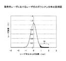
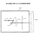
しかし、VCSELの照射強度は中心線より片側において半値幅にて、4°以下程度である。よって、所定の傾斜角度以上傾けて投影窓を設置しないと、フォトダイオードをVCSELに接する程近づけなければならず、できるだけ大きな反射角度を得ようとすると、レーザ光の光スポットの端部の周辺光しか入射させることができない。即ち、図1に示すように、レーザ光は、ガウシアン分布という強度分布を有しているため、特許文献10に記載されているように、レーザ光の光スポットの端部の周辺光だけを反射させてモニタ光として用いる場合には、図1の領域1Aに示される範囲における周辺の強度の低いレーザ光だけをモニタ光として用いることになる。このようにレーザ光の周辺光をモニタ光として用いる場合では、全体にレーザ光の強度に対しモニタ光の強度が極めて低くなるため、信頼性が低くなってしまう。
However, the irradiation intensity of VCSEL is about 4 ° or less at a half-value width on one side from the center line. Therefore, if the projection window is not inclined at a predetermined inclination angle or more, the photodiode must be brought close enough to come into contact with the VCSEL. If an attempt is made to obtain a reflection angle as large as possible, the ambient light at the end of the laser light spot Only incident. That is, as shown in FIG. 1, since the laser light has an intensity distribution called Gaussian distribution, only the ambient light at the end of the light spot of the laser light is reflected as described in
また、面発光レーザにおいては、自身の発光による温度変化により照射角度は若干変動するため、レーザ光の周辺光において強度のばらつきが生じるが、このばらつきはレーザ光の全体におけるばらつきに対し極めて大きい。このため、レーザ光の周辺光をモニタ光として用いることは現実的ではない。よって、モニタ光としては、レーザ光におけるガウシアン分布の全体を反映させた反射光等を用いることが望ましい。 Further, in the surface emitting laser, the irradiation angle slightly varies due to the temperature change caused by the light emitted from the surface emitting laser. Therefore, the intensity variation occurs in the ambient light of the laser beam, but this variation is extremely large with respect to the variation in the entire laser beam. For this reason, it is not realistic to use the ambient light of the laser light as the monitor light. Therefore, as the monitor light, it is desirable to use reflected light or the like reflecting the entire Gaussian distribution in the laser light.
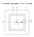
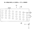
これらの問題点を解決するために、発明者は、図2及び図3に示される光デバイスである面発光レーザモジュールを考案した。この面発光レーザモジュールは、凹部を有するパッケージ10、面発光レーザ素子20、モニタ用のフォトダイオード30、パッケージ10と接合されるリッド40を有している。面発光レーザ素子20は、複数の面発光レーザがアレイ状に形成されているものであり、面発光レーザアレイチップともいう。
In order to solve these problems, the inventor has devised a surface emitting laser module which is the optical device shown in FIGS. This surface emitting laser module includes a
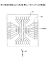
面発光レーザ素子20は、パッケージ10の凹部の底面11に設置されており、凹部の周辺であって底面11よりも高い段部12にモニタ用のフォトダイオード30が設置されている。また、パッケージ10には、リッド40と接合するためのシールリング60が設けられている。また、リッド40には、ガラス等により形成された窓部50が所定の傾斜角度になるように、低融点ガラス41により接続されている。尚、図2はリッドを取り除いた状態の面発光レーザモジュールの上面図であり、図3は、図2における一点鎖線2A−2Bにおいて切断した部分に相当する面発光レーザモジュールの断面図である。また、図2及び図3においては、便宜上、面発光レーザ素子20とパッケージ10のリード配線等とを接続するためのボンディングワイヤ等は省略されている。
The surface
パッケージ10は、セラミックスにより形成されたCLCC(Ceramic Leaded Chip Carrier)と呼ばれるフラットパッケージである。このパッケージ10は、凹部を有しており、セラミックスと複数の不図示のリード配線となる金属配線の多層構造となっている。リッド40は、パッケージ10とシールリング60を介して接合されている。
The
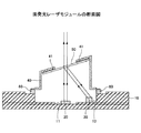
この面発光レーザモジュールでは、リッド40を所望の形状にするために、絞り加工を施した後、窓部50が取り付けられる領域を傾斜させて形成する必要があるが、このような加工は特殊な工程を要するため、コストアップの要因となっていた。尚、リッド40において、窓部50が取り付けられる領域を傾斜させて形成する理由は、面発光レーザ素子20から出射された光が窓部50において反射され、再び面発光レーザ素子20に入射することを防ぐためである。
In this surface emitting laser module, in order to make the
通常、パッケージ10は、セラミックグリーンシート積層法により作製されている。具体的には、セラミックグリーンシートを略垂直に打ち抜き、打ち抜いたシートを上下に重ねて接着し、次に、これらを高温で焼成することにより、焼成体として硬質のパッケージ筐体が形成されている(メタライズ配線工程については省略)。このため、パッケージ10を通常の方法により作製する場合では、図4に示すように、端部に傾斜を有する傾斜部16を形成しようとすると、傾斜部16は階段状に形成される。従って、この上にリッド40をシーム溶接等で密封するためのシールリングを傾斜させて載置しても、隙間ができてしまい内部を完全に密閉することは困難である。よって、密閉性が高く、透明部材を傾斜させて設置することのできるリッドが求められていた。
Usually, the
このように、近年、レーザ素子から出射されるレーザ光の安定性についての要求が厳しく、特許文献1〜3に記載されているレーザ素子及びレーザモジュールでは、その要求を満足させることは困難である。特に、面発光レーザモジュールにおいては、カバーガラスが結露してしまうと、出射されたレーザ光の安定性に影響を与える。また、カバーガラスにより反射された光をモニタし制御するレーザモジュールでは、面発光レーザモジュール内に設けられたフォトダイオードに入射する光量も変動してしまい、レーザ光の安定性を低下させる原因となっている。
As described above, in recent years, the demand for stability of the laser light emitted from the laser element is severe, and it is difficult for the laser element and the laser module described in
本発明は、このような事情の下でなされたものであり、環境信頼性が高く、光量変動の少ない光を出射することのできる光デバイスを低コストで提供することを目的とするものである。 The present invention has been made under such circumstances, and it is an object of the present invention to provide an optical device capable of emitting light with high environmental reliability and little light amount fluctuation at low cost. .
本発明は、基板面に対し垂直方向に光を出射する面発光レーザを有する面発光レーザ素子と、前記面発光レーザ素子を設置するための領域が設けられて、所定の角度で傾斜した傾斜部を上面に有するパッケージと、透明な材料により形成された窓部を含み、前記パッケージの傾斜部と接合される平板状リッドと、を有し、前記パッケージと前記平板状リッドとを接合することにより、前記面発光レーザが覆われるものであって、前記傾斜部は、積層されている複数の層の端の部分により構成され、前記傾斜部の表面は段差を無くしたなめらかな形状であり、前記傾斜部にはシールリングが固定されており、前記シールリングと前記平板状リッドとは溶接により接合されているものであることを特徴とする。 The present invention provides a surface-emitting laser element having a surface-emitting laser that emits light in a direction perpendicular to the substrate surface, and an inclined portion that is inclined at a predetermined angle provided with a region for installing the surface-emitting laser element. And a flat lid that includes a window portion formed of a transparent material and is joined to the inclined portion of the package, and joining the package and the flat lid. The surface-emitting laser is covered, and the inclined portion is constituted by end portions of a plurality of stacked layers , and the surface of the inclined portion has a smooth shape with no step , A seal ring is fixed to the inclined portion, and the seal ring and the flat lid are joined by welding.
本発明によれば、環境信頼性が高く、光量変動の少ない光を出射することのできる光デバイスを低コストで提供することができる。 According to the present invention, it is possible to provide an optical device that can emit light with high environmental reliability and little light amount fluctuation at low cost.
本発明の実施の形態について説明する
〔第1の実施の形態〕
第1の実施の形態における光デバイスは、複数の面発光レーザにより構成される面発光レーザアレイを有する面発光レーザモジュールである。
Embodiments of the present invention will be described [First Embodiment]
The optical device according to the first embodiment is a surface emitting laser module having a surface emitting laser array composed of a plurality of surface emitting lasers.
前述のとおり、これまでの面発光レーザを用いた光源モジュールは端面発光レーザを用いた光源モジュールと異なり、モニタ光学系を必要としていた。このようにモニタ光学系を有する光源ユニット400は、一例として図5に示されるように、レーザモジュール500と光学モジュール600とで構成されていた。
As described above, a light source module using a surface emitting laser so far requires a monitor optical system unlike a light source module using an edge emitting laser. As described above, the
このレーザモジュール500は、面発光レーザモジュール510、この面発光レーザモジュール510を駆動制御する不図示のレーザ制御装置、この面発光レーザモジュール510及びレーザ制御装置が実装されているPCB(Printed Circuit Board)基板580を有している。
This
また、光学モジュール600は、第1の部分610と第2の部分630から構成されている。第1の部分610は、ハーフミラー611、集光レンズ612、及びフォトダイオード613を有している。また、第2の部分630は、カップリングレンズ631、及び開口板632を有している。
The
第1の部分610は、面発光レーザモジュール510の+Z側であって、面発光レーザアレイチップから出射された光の光路上にハーフミラー611が位置するように配置されている。ハーフミラー611に入射した光の一部は−Y方向に反射され、集光レンズ612を介してフォトダイオード613で受光される。フォトダイオード613は、モニタ用フォトダイオードとなっており、受光光量に応じた信号(光電変換信号)をレーザモジュール500のレーザ制御装置に出力する。
The
第2の部分630は、第1の部分610の+Z側であって、ハーフミラー611を透過した光の光路上にカップリングレンズ631が位置するように配置されている。カップリングレンズ631は、ハーフミラー611を透過した光を略平行光とする。開口板632は、開口部を有し、カップリングレンズ631を介した光を整形する。開口板632の開口部を通過した光が、光源ユニット400から出射される光となる。
The
しかしながら、このモニタ用のフォトダイオード613にレーザ光を導入する光学系を組み込むコストが、これら光源ユニット400の高価格化の原因となっていた。このため、図2及び図3に示す構造の面発光レーザモジュールとすることにより、低コストにすることができ、窓部50における反射光が面発光レーザにおける活性層内に侵入することを防ぐことができ、ダストの侵入を防止しつつ、光量変動が少なく、安定したレーザ発振を行なうことができる。尚、このような構造の面発光レーザモジュールでは、窓部50が取り付けられている金属製のリッド40をパッケージ10に設置されたシールリング60を用い、シーム溶接により接合されており、結露による不具合が生じないことが確認されている。
However, the cost of incorporating an optical system for introducing laser light into the
しかしながら、このような形状の金属製のリッド40は、手間のかかる絞り加工等を施し形成されるものであるため、このようにして作製された面発光レーザモジュールはコストをあまり低下させることができず高コストなものとなってしまう。
However, since the
(光デバイス)
次に、図6に基づき本実施の形態における光デバイスについて説明する。本実施の形態における光デバイスは、面発光レーザモジュールであり、凹部を有するパッケージ110、面発光レーザ素子120、モニタ用のフォトダイオード(受光素子)130、パッケージ110に接合される平板状リッド140を有している。面発光レーザ素子120は、複数の面発光レーザがアレイ状に形成されているものであり、面発光レーザアレイチップともいう。尚、図6においては、便宜上、面発光レーザ素子120とパッケージ110のリード配線等とを接続するためのボンディングワイヤ等は省略されている。また、面発光レーザ素子120への戻り光の入射を防ぐことを目的とする場合には、フォトダイオード130を有しない構成であってもよい。
(Optical device)
Next, the optical device in the present embodiment will be described with reference to FIG. The optical device in the present embodiment is a surface emitting laser module, and includes a
面発光レーザ素子120は、パッケージ110の凹部の底面111に設置されており、凹部の周辺部分であって底面111よりも高い段部112にモニタ用のフォトダイオード130が設置されている。
The surface emitting
平板状リッド140は、平板状に形成されており、面発光レーザ素子120からの光を透過する窓部150が低融点ガラス141により接続されている。窓部150は、面発光レーザ素子120の面発光レーザから出射された光が、再び光を出射した面発光レーザに戻らないように、面発光レーザの出射光に垂直な面に対し所定の角度で傾斜するように形成されている。即ち、面発光レーザ素子120のレーザ光の出射面に対し所定の角度で傾斜するように窓部150が接続されている。尚、この傾斜角度は、面発光レーザからの出射光のうち、窓部150において反射した反射光がフォトダイオード130に入射するように、所定の角度となるように形成されている。具体的には、本実施の形態では、この傾斜角度は、約17°となるように形成されているが、傾斜角度は、10°以上、25°以下であることが好ましい。
The
パッケージ110は、セラミックスにより形成されたCLCCと呼ばれるフラットパッケージである。このパッケージ110は、凹部を有しており、セラミックスと複数の不図示のリード配線となる金属配線の多層構造となっている。
このリード配線は、面発光レーザ素子120が設置される領域より放射状に外側に向かって伸びるように形成されており、パッケージ110の内部の金属配線を介し、パッケージ110の外側の不図示の電極端子と接続されている。
The lead wiring is formed so as to extend radially outward from the region where the surface emitting
また、パッケージ110には、平板状リッド140を所定の角度で接合することができるようバッケージ上部110aが設けられており、パッケージ110の上面となるバッケージ上部110aの上端の傾斜部116には、シールリング160が銀ろう等のメタライズペーストにより接着されている。また、平板状リッド140は、この所定の角度で傾斜しているシールリング160に溶接することにより接合される。これにより、シールリング160を介し、パッケージ110と平板状リッド140により、密封することができる。バッケージ上部110aは、パッケージ110の底面111に対し略垂直に延びるように形成されており、傾斜部116において、窓部150が所定の角度で設置することができるように形成されている。尚、バッケージ上部110aはパッケージ110の一部でありセラミックスにより形成されている。
Further, the
また、面発光レーザ素子120が設置される領域には、金属膜が設けられており、この金属膜は、ダイアタッチエリアとも呼ばれるものであり、共通電極になっている。面発光レーザ素子120は、この金属膜上にAuSn等の半田材を用いてダイボンドされており、このようにして、面発光レーザ素子120は、凹部の底面に設置される。
Further, a metal film is provided in a region where the surface emitting
また、フォトダイオード130は、段部112においてダイボンドされている、フォトダイオード130のアノード電極とパッケージ110の金属配線とがワイヤボンディングにより電気的に接続され、裏面に形成されたフォトダイオード130のカソードは導電性接着剤により接地されている。
In the
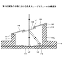
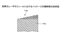
本実施の形態において、パッケージ110は、セラミックグリーンシート積層法により形成されている。具体的には、セラミックグリーンシートを略垂直に打ち抜き、打ち抜いたシートを上下に重ねて接着し、次に、これらを高温で焼成することにより、焼成体として硬質のパッケージ筐体が形成されている(メタライズ配線工程については省略)。このような方法により形成した場合では、図7に示すように、端の傾斜部116aとなる部分が階段状に形成されるため、この上に平板状リッド140を接合しても、隙間ができてしまい内部を完全に密閉することは困難である。
In the present embodiment, the
本実施の形態では、パッケージ110における傾斜部116は、表面がなめらかな形状となるように形成されている。具体的には、図8に示すように、階段状に形成されている部分を銀ろう等のメタライズペースト117により埋めることにより、表面がなめらかな傾斜部116bを形成している。また、図9に示すように、端の部分に傾斜を有するセラミックグリーンシートを積層した構造のものや、セラミックグリーンシートを積層した後、研磨等により表面がなめらかな傾斜を形成することにより傾斜部116cを形成してもよい。このようにして、パッケージ110におけるバッケージ上部110aの上端の傾斜部116の表面をなめらかに形成することにより、シールリング160を高い密着性で接着することができる。
In the present embodiment, the inclined portion 116 in the
この後、シールリング160に平板状リッド140を溶接等により接合することにより、容易に窓部150が所定の角度となるように接合することができる。また、シールリング160が接合されるパッケージ110の傾斜部116は、なめらかな形状で形成されているため、密封性の高い封止を行なうことができる。
Thereafter, the
平板状リッド140は、図2及び図3に示すリッド40のような絞り加工等を施すことなく、低コストで容易に作製をすることができる。また、透明部材(ガラスなど)を取り付けるための窓部を開けた平面状のリッドには、透明部材を低融点ガラスなどで融着する。そしてそのリッドをシールリング160にシーム溶接などの手段によって封止することで、パッケージ内部を完全に密封することができる。このようにして、低コストで密封性の高い面発光レーザモジュールを得ることができる。よって、本実施の形態における面発光レーザモジュールでは、ダストの侵入を防止し、光量変動が少なく安定したレーザ発振を行なうことができる。また、面発光レーザモジュール内部に水分が侵入することもなくなるため、水分による結露等による不具合も防止することができ、酸素等も透過しないため面発光レーザモジュール内部の面発光レーザ素子120の腐食も完全に防止することができる。
The
(窓部の反射率)
ところで、窓部150における反射光をモニタ光として用いる場合、2つの問題点を有している。1つは、膜等が形成されていない窓部150の反射率が上下面合わせても4〜5%程度と低いこと(例えば、780nmの波長にて)であり、この程度の反射率ではフォトダイオードに入射させるモニタ光としては光量が低すぎ、十分な起電流を発生させることができない。即ち、モニタ光の光量をフォトダイオードで検出し、面発光レーザの光強度を制御するが、フォトダイオードにより検出されたモニタ光の信号が小さいと、ノイズに埋もれてしまい、S/Nが低下するため、面発光レーザの制御を正確に行なうことができなくなる。このように、モニタ光により生じた電流が小さいと、面発光レーザの制御を適切に行なうことができない。
(Reflectance of window)
By the way, when using the reflected light in the
もう1つは、窓部150となる透明部材の上面と下面とにおける反射光の干渉によりエタロン効果が生じることである。特に、面発光レーザでは、温度による周波数変動が顕著であり、これにより、モニタ光の強度に振動が生じ、モニタ光が線型性を有しないものとなる。
The other is that the etalon effect is caused by interference of reflected light between the upper surface and the lower surface of the transparent member that becomes the
そこで、本発明者は検討の末、窓部150となる透明部材の下面において反射層を形成し、この反射層による反射率が7〜15%、より好ましくは、9〜12%程度とすることにより、面発光レーザの制御を良好に行なうことができることを見出した。この反射層による反射率は、あまりに低いと、モニタ光により発生する電流が小さくなり、信号がノイズに埋もれてしまい好ましくなく、また、あまりに高いと、面発光レーザによる発光の多くがモニタ光となるため、出射されるレーザ光の光量が低下してしまい好ましくない。よって、反射層における反射率は、上記範囲であることが好ましい。このような反射層は、誘電体膜、誘電体多層膜又は、光を透過する薄い金属膜等により形成されている。
Therefore, the present inventor forms a reflective layer on the lower surface of the transparent member that becomes the
また、窓部150となる透明部材の上面には、反射防止膜が形成されており、この反射防止膜により、反射率が1%以下、更には、0.5%以下となっていることがより好ましい。このような反射防止膜は、誘電体膜又は、誘電体多層膜等により形成されている。
In addition, an antireflection film is formed on the upper surface of the transparent member that becomes the
以上により、同一のモジュール内に面発光レーザ素子120とフォトダイオード130とを設置した面発光レーザモジュールにおいて、十分な光量のモニタ光をフォトダイオードに入射させることが可能となり、エタロン効果によるモニタ光の強度の振動が極めて少なく、安定したモニタ光による電流を得ることができる。
As described above, in the surface emitting laser module in which the surface emitting
(面発光レーザ)
次に、面発光レーザ素子120である面発光レーザアレイチップに形成される面発光レーザについて説明する。面発光レーザアレイは、複数の面発光レーザが2次元的にアレイ状に配列されているものであり、面発光レーザアレイチップは、このような面発光レーザアレイを一つのチップとしたものである。
(Surface emitting laser)
Next, a surface emitting laser formed on the surface emitting laser array chip which is the surface emitting
図10に基づき面発光レーザアレイを構成する一つの面発光レーザ200について説明する。尚、図10(a)は面発光レーザ200のXZ面における断面図であり、図10(b)は面発光レーザ200のYZ面における断面図である。また、本明細書では、前述のとおり、レーザ発振方向をZ軸方向とし、Z軸方向に垂直な面内における互いに直交する2つの方向をX軸方向及びY軸方向として説明する。
One
面発光レーザ200は、発振波長が780nm帯の面発光レーザであり、基板201、バッファ層202、下部半導体DBR203、下部スペーサ層204、活性層205、上部スペーサ層206、上部半導体DBR207、コンタクト層209等を有している。更に、活性層205、上部スペーサ層206、上部半導体DBR207、コンタクト層209及び下部スペーサ層204の一部にはメサ210が形成されている。また、メサ210の側面及び上部には、保護層211が形成されており、更に、メサ210の正面に接続されるp側電極213が形成されており、基板201の裏面にはn側電極214が形成されている。透明層211A及び211Bは、保護膜211が形成される際に同時に形成されている。尚、本実施の形態では、透明層211A及び211Bを小領域と記載する場合があり、透明層211A及び211B等によりモードフィルタが形成される。また、上部DBR207と上部スペーサ層206との間、または、上部DBR207の内部には、電流狭窄層208が形成されており、電流狭窄層208は、メサ210の周辺部分において酸化されている酸化領域208aとメサ210の中央部分で酸化されていない電流狭窄領域208bとを有している。
The
基板201は、表面が鏡面研磨面であり、図11(a)に示されるように、鏡面研磨面(主面)の法線方向が、結晶方位[1 0 0]方向に対して、結晶方位[1 1 1]A方向に向かって15度(θ=15度)傾斜したn−GaAs単結晶基板である。すなわち、基板201はいわゆる傾斜基板である。ここでは、図11(b)に示されるように、結晶方位[0 −1 1]方向が+X方向、結晶方位[0 1 −1]方向が−X方向となるように配置されている。
The surface of the
尚、基板201として、このような傾斜基板を用いることによって、偏光方向を所定の方向、例えば、X軸方向に安定させようとする偏光制御作用が働く。
In addition, by using such an inclined substrate as the
(面発光レーザモジュールの特性の評価)
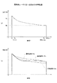
次に、上述した面発光レーザ素子により形成される面発光レーザモジュールの特性について説明する。面発光レーザモジュール及び光源ユニットとして、図5に示した構造を模した光学系を利用して特性の評価を行った。特性評価は、出射された光の光量をフォトダイオード(PD)にて検出することにより行なう。得られる理想的な波形データを図12(a)に示すが、戻り光の影響を受けると、光量が不安定となり変動が生じる。図12(b)において模式的に、光量変動のない正常波形125aと光量変動がある場合の異常波形125b及び125cをと比較して示す。図12(b)に示されるように、異常波形125b及び125cは、波形の前半部分に波を打つように現れることが多いが、これに限らず、後半部分に波を打つように現れる場合もある。また、周波数も1kHzの場合や、もっと大きい、例えば、数100kHzの波形においても、波形変動が生じる場合がある。特に、1kHzにおける波形を画像形成装置に必要な1ラインを安定して描く際の基準とした場合、その安定性は画像形成装置によっては、数%レベル、例えば、5%レベルの変動であっても問題となる。ここで、画像形成装置に必要な特性として、この特性値を定量化する方法について説明する。一般的には、熱によるレーザ光量の変動を評価する指標であり、ドループ値として利用されている。具体的には、図12(a)に示すように、レーザ立ち上がり時間帯の光量と、十分に時間が経過した状態の時間帯での光量の差をとる。その一例として、1kHzでデューティー比が50%の波形を示している。
Dr=(Pa−Pb)/Pa
Pa:時間Taにおける光出力値
Pb:時間Tbにおける光出力値
上式で示される数値Dr(単位:%)をドループ値として定義する。本実施の形態では、1kHzでデューティーが50%、Taは1kHzにおける1μsecの位置で、Tbは480μsecの位置とした。光出力は1.4mW相当とし、測定温度は25℃になるように温調冶具で調整した。本実施の形態では上記のような出力、温度としているが、利用される出力値、温度に対して、本測定が行われるので、これに限定されるものではない。また、上記周波数、デューティー比、および、Ta、Tbは、画像形成装置として、高精度な画像を形成する上で、必要な条件となる。
(Evaluation of characteristics of surface emitting laser module)
Next, characteristics of the surface emitting laser module formed by the surface emitting laser element described above will be described. The characteristics of the surface emitting laser module and the light source unit were evaluated using an optical system simulating the structure shown in FIG. The characteristic evaluation is performed by detecting the amount of emitted light with a photodiode (PD). The ideal waveform data obtained is shown in FIG. 12 (a). When affected by the return light, the light quantity becomes unstable and fluctuates. FIG. 12B schematically shows a normal waveform 125a having no light amount fluctuation and an abnormal waveform 125b and 125c when there is a light amount fluctuation. As shown in FIG. 12B, the abnormal waveforms 125b and 125c often appear to wave in the first half of the waveform. However, the present invention is not limited to this, and the abnormal waveforms 125b and 125c may appear to wave in the second half. is there. In addition, waveform fluctuation may occur even when the frequency is 1 kHz or even a larger waveform, for example, several hundred kHz. In particular, when the waveform at 1 kHz is used as a reference for stably drawing one line necessary for the image forming apparatus, the stability is a fluctuation of several percent level, for example, 5% level depending on the image forming apparatus. Is also a problem. Here, a method for quantifying the characteristic value as a characteristic necessary for the image forming apparatus will be described. Generally, it is an index for evaluating fluctuations in the amount of laser light due to heat, and is used as a droop value. Specifically, as shown in FIG. 12A, the difference between the light amount in the laser rising time zone and the light amount in the time zone in which sufficient time has elapsed is taken. As an example, a waveform having a duty ratio of 50% at 1 kHz is shown.
Dr = (Pa−Pb) / Pa
Pa: Light output value at time Ta Pb: Light output value at time Tb A numerical value Dr (unit:%) represented by the above equation is defined as a droop value. In this embodiment, the duty is 50% at 1 kHz, Ta is 1 μsec at 1 kHz, and Tb is 480 μsec. The light output was adjusted to 1.4 mW and the measurement temperature was adjusted to 25 ° C. with a temperature control jig. In the present embodiment, the output and temperature are set as described above. However, the present measurement is performed on the output value and temperature used, and the present invention is not limited to this. The frequency, duty ratio, and Ta and Tb are necessary conditions for forming a highly accurate image as an image forming apparatus.
また、面発光レーザを複数配列し面発光レーザアレイとした場合、1つ1つのドループ値が一致してないと、形成される画像の視認性が著しく悪化する。面発光レーザアレイの特性として、ドループ値の最大値と最小値の差(以下これをばらつきと表現する)を小さくする必要がある。しかし、先の異常波形125b及び125c等が現れると、ばらつきは大きくなる。そこで、このドループ値のばらつきを以下の式に満たすことを条件とした。
ドループのばらつき(%)=Dr(max)−Dr(min)
Dr(max):複数ある素子の中で最もDr値が大きい素子のDr値
Dr(min):複数ある素子の中で最もDr値が小さい素子のDr値
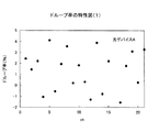
図13には、21個の発光部(ch1〜ch21)を有する面発光レーザアレイ、及び無反射層を表面にコーティングしていない透明部材との一体型樹脂リッド(反射率:約5.2%)を有し、この透明部材を面発光レーザアレイの出射面に対して傾斜させていない面発光レーザモジュール(光デバイスAという)におけるドループ率を示す。尚、各発光部には、モードフィルタは設けられていない。
Further, when a plurality of surface emitting lasers are arranged to form a surface emitting laser array, the visibility of the formed image is significantly deteriorated unless the respective droop values are matched. As a characteristic of the surface emitting laser array, it is necessary to reduce a difference between the maximum value and the minimum value of the droop value (hereinafter referred to as variation). However, when the abnormal waveforms 125b and 125c, etc. appear, the variation becomes large. Therefore, the condition is that the variation of the droop value satisfies the following formula.
Droop variation (%) = Dr (max) −Dr (min)
Dr (max): Dr value of the element having the largest Dr value among a plurality of elements Dr (min): Dr value of the element having the smallest Dr value among the plurality of elements FIG. A surface emitting laser array having (ch1 to ch21) and an integrated resin lid (reflectance: about 5.2%) with a transparent member not coated with a nonreflective layer on the surface. The droop rate in a surface emitting laser module (referred to as optical device A) that is not inclined with respect to the emission surface of the light emitting laser array is shown. Note that each light emitting unit is not provided with a mode filter.
ドループ率は、大きいもので4%、小さいものでは−1.5%であった。これは、出力波形が異常波形となっており、その異常形状が、発光部によって一様でないことを示している。無反射コーティングをしていない場合のわずか5.2%という反射率でもこのようなばらつきが観測されてしまう。このように、発光部間にドループ率の大きなばらつきがある面発光レーザモジュールを用いると、高品質な画像を形成することができない。 The droop rate was 4% at large and -1.5% at small. This indicates that the output waveform is an abnormal waveform, and the abnormal shape is not uniform depending on the light emitting unit. Such a variation is observed even with a reflectance of only 5.2% in the case of no antireflection coating. As described above, when a surface emitting laser module having a large variation in the droop rate between the light emitting portions is used, a high quality image cannot be formed.
また、図14には、21個の発光部(ch1〜ch21)を有する面発光レーザアレイ、及びカバーガラスとして高価な無反射ガラス板(反射率:0.1%)を有し、このガラス板を面発光レーザアレイの出射面に対して傾斜させていない面発光レーザモジュール(光デバイスBという)におけるドループ率を示す。尚、各発光部には、モードフィルタは設けられていない。ドループ率は、大きいもので1.5%、小さいもので0.2%であり、飛躍的にばらつきが低減されているのが分かる。 FIG. 14 also shows a surface emitting laser array having 21 light emitting sections (ch1 to ch21) and an expensive non-reflective glass plate (reflectance: 0.1%) as a cover glass. Is a droop rate in a surface emitting laser module (referred to as optical device B) that is not inclined with respect to the emission surface of the surface emitting laser array. Note that each light emitting unit is not provided with a mode filter. The droop rate is 1.5% for a large one and 0.2% for a small one, indicating that the variation is drastically reduced.
このように、反射率が非常に低い高価な無反射ガラスを用いることにより、戻り光への耐性が強くなり、ドループ率のばらつきが小さくなる。そして、異常波形の抑制、光量変動の抑制が可能となる。しかしながら、高価な無反射ガラスの使用は、面発光レーザモジュールの大幅なコスト上昇を招いてしまう。 As described above, by using an expensive non-reflective glass having a very low reflectance, resistance to return light is increased, and variation in droop rate is reduced. In addition, it is possible to suppress abnormal waveforms and light amount fluctuations. However, the use of expensive non-reflective glass causes a significant cost increase of the surface emitting laser module.
そこで、発明者らは、安価な無反射層が表面にコーティングされていない透明部材となるガラスを窓部に用い、この透明部材を傾斜させてドループ率のばらつきを調べた。 Therefore, the inventors used glass, which is a transparent member whose surface is not coated with an inexpensive non-reflective layer, for the window portion, and investigated the variation in the droop rate by inclining the transparent member.
図15には、21個の発光部(ch1〜ch21)を有する面発光レーザアレイ、及び無反射層を表面にコーティングしていない透明部材との一体型樹脂リッド(反射率:5.2%)を有し、樹脂材料のリッドにおける窓部を面発光レーザアレイの出射面に対して8°傾斜させた面発光レーザモジュール(光デバイスCという)におけるドループ率を示す。尚、各発光部には、モードフィルタは設けられていない。ドループ率は、大きいもので3%、小さいもので0.5%であり、上記光デバイスAよりもばらつきが低減されているのが分かる。しかしながら、上記光デバイスBよりもドループ率のばらつきは大きく、傾斜角8°ではまだ充分ではないといえる。 FIG. 15 shows a surface-emitting laser array having 21 light emitting portions (ch1 to ch21) and an integrated resin lid with a transparent member not coated with a nonreflective layer (reflectance: 5.2%). And a droop rate in a surface emitting laser module (referred to as an optical device C) in which a window portion of a lid made of a resin material is inclined by 8 ° with respect to an emission surface of a surface emitting laser array. Note that each light emitting unit is not provided with a mode filter. The droop rate is 3% at the largest and 0.5% at the smallest, and it can be seen that the variation is smaller than that of the optical device A. However, the droop rate variation is larger than that of the optical device B, and an inclination angle of 8 ° is not sufficient.
また、図16には、21個の発光部(ch1〜ch21)を有する面発光レーザアレイ、及び無反射層を表面にコーティングしていない透明部材との一体型樹脂リッド(反射率:5.2%)を有し、樹脂材料のリッドにおける窓部を面発光レーザアレイの出射面に対して10°傾斜させた面発光レーザモジュール(光デバイスDという)におけるドループ率を示す。尚、各発光部には、モードフィルタは設けられていない。 Also, FIG. 16 shows an integrated resin lid (reflectance: 5.2) with a surface emitting laser array having 21 light emitting portions (ch1 to ch21) and a transparent member whose surface is not coated with a nonreflective layer. %) And a droop rate in a surface emitting laser module (referred to as an optical device D) in which a window portion in a lid of a resin material is inclined by 10 ° with respect to an emission surface of a surface emitting laser array. Note that each light emitting unit is not provided with a mode filter.
また、図17には、21個の発光部(ch1〜ch21)を有する面発光レーザアレイ、及び無反射層を表面にコーティングしていない透明部材との一体型樹脂リッド(反射率:5.2%)を有し、樹脂材料のリッドにおける窓部を面発光レーザアレイの出射面に対して15°傾斜させた面発光レーザモジュール(光デバイスEという)におけるドループ率を示す。尚、各発光部には、モードフィルタは設けられていない。 FIG. 17 shows an integrated resin lid (reflectance: 5.2) with a surface-emitting laser array having 21 light-emitting portions (ch1 to ch21) and a transparent member whose surface is not coated with a non-reflective layer. %) And a droop rate in a surface emitting laser module (referred to as an optical device E) in which a window portion in a lid of a resin material is inclined by 15 ° with respect to an emission surface of a surface emitting laser array. Note that each light emitting unit is not provided with a mode filter.
光デバイスD及び光デバイスEでは、ドループ率のばらつきは、光デバイスBと同等、あるいはそれ以下であった。 In the optical device D and the optical device E, the variation in the droop rate was equal to or less than that of the optical device B.
このように、反射防止膜が表面にコーティングされていない透明部材であるガラスを用いても、透明部材を傾斜させることにより、反射防止コーティングされたガラスと同様の効果を得ることができることがわかった。即ち、光を反射する透明部材を用いても、透明部材を傾斜させることにより、戻り光の問題を解決することができる。 As described above, it was found that even when glass, which is a transparent member whose surface is not coated with an antireflection film, is used, the same effect as that of glass coated with antireflection can be obtained by inclining the transparent member. . That is, even if a transparent member that reflects light is used, the problem of return light can be solved by inclining the transparent member.
以上に基づき、本実施の形態においては、透明部材である窓部150の傾斜角が約17°となるように、平板状リッド140及びパッケージ110が形成されている。
Based on the above, in the present embodiment, the
(面発光レーザモジュールの製造方法)
次に、図6に基づいて、本実施の形態における面発光レーザモジュールの製造方法について説明する。
(Method for manufacturing surface emitting laser module)
Next, a method for manufacturing the surface emitting laser module according to the present embodiment will be described with reference to FIG.
最初に、パッケージ110の凹部の底面111に、面発光レーザ素子120である面発光レーザアレイチップをダイボンドする。
First, a surface emitting laser array chip which is the surface emitting
次に、面発光レーザ素子120である面発光レーザアレイチップにおける複数の電極パッドとパッケージ110における複数の不図示のリード(金属配線)とを各々ワイヤボンディングにより電気的に接続する。
Next, a plurality of electrode pads in the surface emitting laser array chip which is the surface emitting
次に、パッケージ110の段部112に、フォトダイオード130をダイボンドする。
Next, the
次に、フォトダイオード130のアノード電極とパッケージ110の不図示のリード配線(金属配線)とをワイヤボンディングにより電気的に接続し、裏面のカソードは導電性接着剤により接地する。
Next, the anode electrode of the
次に、面発光レーザ素子120である面発光レーザアレイチップとフォトダイオード130とが固定され、電気的に接続されているパッケージ110に平板状リッド140を接合する。具体的には、パッケージ110の傾斜部116に銀ろうによりシールリング160を取り付け、シールリング160の上に、平板状リッド140を載置し、シーム溶接を行なうことにより接合し封止する。尚、平板状リッド140には、低融点ガラス141により透明部材であるガラスにより形成された窓部150が接合されており、窓部150には上面に反射防止膜、下面に約10%の反射率を有する反射層が形成されている。尚、窓部150をパッケージ110に平板状リッド140を接合することにより、窓部150の面が、面発光レーザ素子120が形成する面に対し約17°となるようにパッケージ110におけるバッケージ上部110a及び傾斜部116が形成されている。
Next, the surface-emitting
以上のように、窓部150は、面発光レーザ素子120から出射されたレーザ光の出射面に対し、10〜25°の範囲となるように設置されている。よって、傾斜部116は、窓部150の下面において反射された光がフォトダイオード130に入射するように形成されている。
As described above, the
これにより、高コスト化を招くことなく、光量変動が少なく安定した光を出射することのできる面発光レーザモジュールとなる光デバイスを得ることができる。 As a result, an optical device that is a surface-emitting laser module that can emit stable light with little fluctuation in the amount of light without increasing the cost can be obtained.
また、面発光レーザ素子120における発光部は各々レーザ光の出射面が誘電体膜で覆われており、半導体層が露出していないため、出射領域における酸化や汚染を防ぐことができる。また、レーザ光の出射領域の中心部は、光学的な厚さがλ/4の偶数倍となる誘電体膜により覆われているため、誘電体膜が形成されていない場合と同等となり、反射率を低下させることがない。
Further, each of the light emitting portions in the surface emitting
また、本実施の形態においては、小領域となる透明層211A及び211Bの形状が長方形である場合について説明したが、これに限定されるものではなく、例えば、図18に示すように、p側電極213の開口部内において、小領域となる透明層211C及び211Dは輪帯状のものを2つに分割した形状に形成したものであってもよい。この際、モードフィルタとなる透明層211C及び211Dは、光学的な厚さがλ/4のSiNからなる保護膜211を形成する際に同時に形成される。
Further, in the present embodiment, the case where the
また、図19に示すように、所望の偏光方向PをY軸方向とする場合には、p側電極213の開口部内において、小領域となる透明層211A及び211Bの長手方向をX軸方向とすればよい。
As shown in FIG. 19, when the desired polarization direction P is the Y-axis direction, the longitudinal direction of the
更に、偏光方向を考慮する必要がない場合には、等方的に形成してもよい。即ち、p側電極213の開口部内において、図20に示されるように、透明層231Aとなる低反射率領域を方形状(方形状の開口部を有する)に形成してもよく、また、図21に示されるように、透明層231Bとなる低反射率領域を輪帯状に形成してもよい。
Further, when there is no need to consider the polarization direction, it may be formed isotropically. That is, in the opening of the p-
また、本実施の形態は、図22に示されるように、保護膜217を形成したもの、即ち、小領域となる透明層211A及び211B上に保護膜217を形成することにより、小領域となる透明層221A及び221Bを形成したものであってもよい。また、保護層211及び保護層217としてはSiNが用いられるが、これに限らず、例えば、SiNx、SiOx、TiOx及びSiONのいずれかであってもよい。それぞれの材料の屈折率に合わせて膜厚を設計することにより、同様の効果を得ることができる。また、各モードフィルタは保護層211及び保護層217と同じ材料であってもよく、また、異なる材料であってもよい。
Further, in the present embodiment, as shown in FIG. 22, a small region is formed by forming the
また、本実施の形態では、基板の主面の法線方向が、結晶方位[1 0 0]方向に対して、結晶方位[1 1 1]A方向に向かって15°傾斜している場合について、一例として説明したが、これに限定されるものではなく、基板の主面の法線方向が、結晶方位[1 0 0]の一の方向に対して、結晶方位[1 1 1]の一の方向に向かって傾斜していればよい。また、本実施の形態では、基板が傾斜基板の場合について説明したが、これに限定されるものではなく、非傾斜基板ではない基板を用いてもよい。 In the present embodiment, the normal direction of the main surface of the substrate is inclined by 15 ° toward the crystal orientation [1 1 1] A direction with respect to the crystal orientation [1 0 0] direction. However, the present invention is not limited to this. The normal direction of the main surface of the substrate is one of the crystal orientations [1 1 1] with respect to one direction of the crystal orientation [1 0 0]. It suffices if it is inclined toward the direction. In this embodiment, the case where the substrate is a tilted substrate has been described. However, the present invention is not limited to this, and a substrate that is not a non-tilted substrate may be used.
(面発光レーザアレイ)
次に、本実施の形態における面発光レーザアレイについて説明する。本実施の形態における面発光レーザアレイは、上述した面発光レーザが2次元的に複数形成されているものである。
(Surface emitting laser array)
Next, the surface emitting laser array in the present embodiment will be described. The surface emitting laser array according to the present embodiment is formed by two-dimensionally forming the above-described surface emitting lasers.
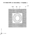
図23に基づき、本実施の形態における面発光レーザアレイ240について説明する。本実施の形態における面発光レーザアレイ240は、複数(ここでは32個)の発光部300となる面発光レーザが同一基板上に配置されている。尚、X軸方向は主走査対応方向であり、Y軸方向は副走査対応方向である。複数の発光部300は、すべての発光部300をY軸方向に伸びる仮想線上に正射影したときに等間隔d2となるように配置されている。このようにして、32個の発光部300は2次元的に配列されている。また、本明細書では、「発光部間隔」とは2つの発光部300の中心間距離を意味する。また、図23では発光部300の数が32個であるものを示しているが、発光部300の個数は、複数であればよく、例えば、発光部300が40個のものであってもよい。また、本実施の形態においては、発光部300は発振波長が780nmであるものとする。
Based on FIG. 23, the surface emitting
図24には、図23における破線23A−23Bにおいて切断した断面図を示す。本実施の形態における面発光レーザアレイ240において、各発光部300は、前述した面発光レーザ200により構成されている。このため、面発光レーザアレイ240は、前述した面発光レーザ200と同様な方法により製造することが可能である。これにより、各発光部300間で均一な偏光方向を持つ単一基本横モードの複数のレーザ光を発する面発光レーザアレイを得ることができる。このようにして得られた面発光レーザアレイ240により、円形で且つ光密度の高い微小な光スポットを32個同時に、後述する感光体ドラム上に形成することが可能となる。
24 is a cross-sectional view taken along the
また、面発光レーザアレイ240では、各発光部を副走査対応方向に延びる仮想線上に正射影したときの発光部間隔が等間隔d2であるので、点灯のタイミングを調整することにより、後述する感光体ドラム上において副走査方向に等間隔で発光部が並んでいる場合と同様な構成と捉えることができる。
Further, in the surface emitting
そして、例えば、上記間隔d2を2.65μm、後述する光走査装置の光学系の倍率を2倍とすれば、4800dpi(ドット/インチ)の高密度書込みができる。もちろん、主走査対応方向の発光部数を増加したり、副走査対応方向のピッチd1を狭くして間隔d2を更に小さくした構成のアレイ配置としたり、光学系の倍率を下げる等を行えばより高密度化することが可能であり、より高品質の印刷が可能となる。なお、主走査方向の書き込み間隔は、発光部の点灯のタイミングで容易に制御できる。 For example, if the distance d2 is 2.65 μm and the magnification of the optical system of the optical scanning device described later is doubled, high-density writing of 4800 dpi (dots / inch) can be performed. Of course, if the number of light emitting portions in the main scanning direction is increased, the array arrangement is configured such that the pitch d1 in the sub scanning direction is narrowed and the interval d2 is further reduced, or the magnification of the optical system is reduced, the higher the number. Densification is possible, and higher quality printing is possible. Note that the writing interval in the main scanning direction can be easily controlled by the lighting timing of the light emitting unit.
ところで、本実施の形態における面発光レーザアレイ240において、隣接する2つの発光部300の間の溝は、各発光部の電気的及び空間的分離のために、5μm以上であることが好ましい。あまり狭いと製造時のエッチングの制御が難しくなるからである。また、メサ210の大きさ(1辺の長さ)は10μm以上であることが好ましい。あまり小さいと動作時に熱がこもり、特性が低下するおそれがあるからである。
By the way, in the surface emitting
尚、図25には、面発光レーザアレイ240における配線構造を示す。このように面発光レーザアレイ240では、2次元的に配列されている32個の発光部300、及び32個の発光部の周囲に設けられ各発光部300に対応した32個の電極パッド310を有している。また、各電極パッド310は、対応する発光部300と配線部材320によって電気的に接続されている。
FIG. 25 shows a wiring structure in the surface emitting
また、上述した2次元的に面発光レーザ200が配列された面発光レーザアレイ240に代えて、発光部300となる面発光レーザ200が1次元配列された面発光レーザアレイを用いてもよい。
Further, instead of the surface emitting
また、本実施の形態では、面発光レーザ200となる発光部300の波長が780nm帯の場合について説明したが、これに限定されるものではなく、画像形成装置の感光体等の特性に応じて、発光部300における発振波長を変更してもよい。具体的には、650nm帯、850nm帯、980nm帯、1.3μm帯、1.5μm帯等の波長であってもよい。この場合、活性層を構成する半導体材料は、発振波長に応じた混晶半導体材料が用いられる。例えば、650nm帯では、AlGaInP系混晶半導体材料、980帯ではInGaAs系混晶半導体材料、1.3μm帯及び1.5μm帯では、GaInNAs(Sb)系混晶半導体材料を用いることができる。
In the present embodiment, the case where the wavelength of the
また、上部反射鏡及び下部反射鏡となる上部半導体DBR及び下部半導体DBRは、発振波長に対応して材料及び構成を選択して作製される。例えば、AlGaInP系混晶半導体材料等のAlGaAs系混晶半導体材料以外のものを用いることができる。尚、上部半導体DBR及び下部半導体DBRを形成するための低屈折率材料及び光屈折率材料は、共に発振波長に対して透明であって、かつ、相互における屈折率差が可能な限り大きいくなる材料を選択して形成されていることが好ましい。 In addition, the upper semiconductor DBR and the lower semiconductor DBR that serve as the upper reflector and the lower reflector are manufactured by selecting materials and configurations corresponding to the oscillation wavelength. For example, a material other than an AlGaAs mixed crystal semiconductor material such as an AlGaInP mixed crystal semiconductor material can be used. Note that the low refractive index material and the light refractive index material for forming the upper semiconductor DBR and the lower semiconductor DBR are both transparent to the oscillation wavelength, and the refractive index difference between them is as large as possible. It is preferably formed by selecting a material.
〔第2の実施の形態〕
次に、第2の実施の形態について説明する。本実施の形態は、第1の実施の形態における面発光レーザモジュールを用いた光走査装置1010及び画像形成装置としてのレーザプリンタ1000である。
[Second Embodiment]
Next, a second embodiment will be described. This embodiment is an
図26に基づき、本実施の形態におけるレーザプリンタ1000について説明する。本実施の形態におけるレーザプリンタ1000は、光走査装置1010、感光体ドラム1030、帯電チャージャ1031、現像ローラ1032、転写チャージャ1033、除電ユニット1034、クリーニングユニット1035、トナーカートリッジ1036、給紙コロ1037、給紙トレイ1038、レジストローラ対1039、定着ローラ1041、排紙ローラ1042、排紙トレイ1043、通信制御装置1050、及び上記各部を統括的に制御するプリンタ制御装置1060等を備えている。なお、これらは、プリンタ筐体1044の中の所定位置に収容されている。
Based on FIG. 26, the
通信制御装置1050は、ネットワークなどを介した上位装置(例えばパソコン)との双方向の通信を制御する。
The
感光体ドラム1030は、円柱状の部材であり、その表面には感光層が形成されている。すなわち、感光体ドラム1030の表面が被走査面である。そして、感光体ドラム1030は、矢印Xで示す方向に回転するようになっている。
The
帯電チャージャ1031、現像ローラ1032、転写チャージャ1033、除電ユニット1034及びクリーニングユニット1035は、それぞれ感光体ドラム1030の表面近傍に配置されている。そして、感光体ドラム1030の回転方向に沿って、帯電チャージャ1031→現像ローラ1032→転写チャージャ1033→除電ユニット1034→クリーニングユニット1035の順に配置されている。
The charging
帯電チャージャ1031は、感光体ドラム1030の表面を均一に帯電させる。
The charging
光走査装置1010は、帯電チャージャ1031で帯電された感光体ドラム1030の表面を、上位装置からの画像情報に基づいて変調された光束により走査し、感光体ドラム1030の表面に画像情報に対応した潜像を形成する。ここで形成された潜像は、感光体ドラム1030の回転に伴って現像ローラ1032の方向に移動する。なお、この光走査装置1010の構成については後述する。
The
トナーカートリッジ1036にはトナーが格納されており、このトナーは現像ローラ1032に供給される。
現像ローラ1032は、感光体ドラム1030の表面に形成された潜像にトナーカートリッジ1036から供給されたトナーを付着させて画像情報を顕像化させる。ここでトナーが付着した潜像(以下では、便宜上「トナー像」ともいう)は、感光体ドラム1030の回転に伴って転写チャージャ1033の方向に移動する。
The developing
給紙トレイ1038には記録紙1040が格納されている。この給紙トレイ1038の近傍には給紙コロ1037が配置されており、この給紙コロ1037は、記録紙1040を給紙トレイ1038から1枚づつ取り出し、レジストローラ対1039に搬送する。このレジストローラ対1039は、給紙コロ1037によって取り出された記録紙1040を一旦保持するとともに、この記録紙1040を感光体ドラム1030の回転に合わせて感光体ドラム1030と転写チャージャ1033との間隙に向けて送り出す。
転写チャージャ1033には、感光体ドラム1030の表面のトナーを電気的に記録紙1040に引きつけるために、トナーとは逆極性の電圧が印加されている。この電圧により、感光体ドラム1030の表面のトナー像が記録紙1040に転写される。ここで転写された記録紙1040は、定着ローラ1041に送られる。
A voltage having a polarity opposite to that of the toner is applied to the
定着ローラ1041では、熱と圧力とが記録紙1040に加えられ、これによってトナーが記録紙1040上に定着される。ここで定着された記録紙1040は、排紙ローラ1042を介して排紙トレイ1043に送られ、排紙トレイ1043上に順次スタックされる。
In the fixing
除電ユニット1034は、感光体ドラム1030の表面を除電する。
The
クリーニングユニット1035は、感光体ドラム1030の表面に残ったトナー(残留トナー)を除去する。残留トナーが除去された感光体ドラム1030の表面は、再度帯電チャージャ1031に対向する位置に戻る。
The
次に、図27に基づき光走査装置1010について説明する。光走査装置1010は、偏向器側走査レンズ1111a、像面側走査レンズ1111b、ポリゴンミラー1113、光源ユニット1114、シリンドリカルレンズ1117、反射ミラー1118、及び走査制御装置(図示省略)などを備えている。そして、これらは、光学ハウジング1030の所定位置に組み付けられている。尚、光源ユニット1114は、第1の実施の形態における面発光レーザモジュールを含む光源ユニット1114が用いられている。
Next, the
また、本明細書では、光源ユニット1114からの光の出射方向をZ軸方向、このZ軸方向に垂直な平面内で互いに直交する2つの方向をX軸方向及びY軸方向として説明する。また、便宜上、主走査方向に対応する方向を「主走査対応方向」と記載し、副走査方向に対応する方向を「副走査対応方向」と記載する場合がある。
In the present specification, the light emission direction from the
シリンドリカルレンズ1117は、光源ユニット1114から出射された光を、反射ミラー1118を介してポリゴンミラー1113の偏向反射面近傍に集光する。
The
面発光レーザ120とポリゴンミラー1113との間の光路上に配置される光学系は、偏向器前光学系とも呼ばれている。本実施形態では、偏向器前光学系は、カップリングレンズと開口板とシリンドリカルレンズ1117と反射ミラー1118とから構成されている。
The optical system arranged on the optical path between the
ポリゴンミラー1113は、高さの低い正六角柱状部材からなり、側面に6面の偏向反射面が形成されている。そして、不図示の回転機構により、図27に示される矢印の方向に一定の角速度で回転されている。従って、光源ユニット1114から出射され、シリンドリカルレンズ1117によってポリゴンミラー1113の偏向反射面近傍に集光された光は、ポリゴンミラー1113の回転により一定の角速度で偏向される。
The
偏向器側走査レンズ1111aは、ポリゴンミラー1113で偏向された光の光路上に配置されている。像面側走査レンズ1111bは、偏向器側走査レンズ1111aを介した光の光路上に配置されている。そして、この像面側走査レンズ1111bを介した光が、感光体ドラム1030の表面に照射され、光スポットが形成される。この光スポットは、ポリゴンミラー1113の回転に伴って感光体ドラム1030の長手方向に移動する。即ち、感光体ドラム1030上を走査する。このときの光スポットの移動方向が「主走査方向」である。また、感光体ドラム1030の回転方向が「副走査方向」である。
The deflector-
ポリゴンミラー1113と感光体ドラム1030との間の光路上に配置される光学系は、走査光学系とも呼ばれている。本実施形態では、走査光学系は、偏向器側走査レンズ1111aと像面側走査レンズ1111bとから構成されている。なお、ポリゴンミラー1113と偏向器側走査レンズ1111aとの間の光路上、偏向器側走査レンズ1111aと像面側走査レンズ1111bの間の光路上、及び像面側走査レンズ1111bと感光体ドラム1030の間の光路上の少なくともいずれかに、少なくとも1つの折り返しミラーが配置されてもよい。
The optical system arranged on the optical path between the
本実施の形態におけるレーザプリンタ1000では、第1の実施の形態における面発光レーザモジュールを用いているため、レーザプリンタ1000では書きこみドット密度が上昇しても印刷速度を落とすことなく印刷することができる。また、同じ書きこみドット密度の場合には印刷速度を更に速くすることができる。
Since the
また、この場合には、各発光部からの光束の偏光方向が安定して揃っているため、レーザプリンタ1000では、高品質の画像を安定して形成することができる。
In this case, since the polarization directions of the light beams from the respective light emitting units are stably aligned, the
尚、本実施の形態における説明では、画像形成装置としてレーザプリンタ1000の場合について説明したが、これに限定されるものではない。
In the description of the present embodiment, the case of the
例えば、レーザ光によって発色する媒体(例えば、用紙)に直接、レーザ光を照射する画像形成装置であってもよい。 For example, an image forming apparatus that directly irradiates laser light onto a medium (for example, paper) that develops color with laser light may be used.
例えば、媒体が、CTP(Computer to Plate)として知られている
印刷版であってもよい。つまり、光走査装置1010は、印刷版材料にレーザアブレーシ
ョンによって直接画像形成を行い、印刷版を形成する画像形成装置にも好適である。
For example, the medium may be a printing plate known as CTP (Computer to Plate). That is, the
また、例えば、媒体が、いわゆるリライタブルペーパーであってもよい。これは、例え
ば紙や樹脂フィルム等の支持体上に、以下に説明するような材料が記録層として塗布され
ている。そして、レーザ光による熱エネルギー制御によって発色に可逆性を与え、表示/
消去を可逆的に行うものである。
For example, the medium may be so-called rewritable paper. For example, a material described below is applied as a recording layer on a support such as paper or a resin film. Then, reversibility is imparted to the color by thermal energy control by laser light, and display /
Erasing is performed reversibly.
透明白濁型リライタブルマーキング法とロイコ染料を用いた発消色型リライタブルマー
キング法があり、いずれも適用できる。
There are a transparent cloudy type rewritable marking method and a color developing / erasing type rewritable marking method using a leuco dye, both of which can be applied.
透明白濁型は、高分子薄膜の中に脂肪酸の微粒子を分散したもので、110℃以上に加
熱すると脂肪酸の溶融により樹脂が膨張する。その後、冷却すると脂肪酸は過冷却状態に
なり液体のまま存在し、膨張した樹脂が固化する。その後、脂肪酸が固化収縮して多結晶
の微粒子となり樹脂と微粒子間に空隙が生まれる.この空隙により光が散乱されて白色に
見える。次に、80℃から110℃の消去温度範囲に加熱すると、脂肪酸は一部溶融し、
樹脂は熱膨張して空隙を埋める。この状態で冷却すると透明状態となり画像の消去が行わ
れる。
The transparent cloudy type is a polymer thin film in which fine particles of fatty acid are dispersed. When heated to 110 ° C. or higher, the resin expands due to melting of the fatty acid. Thereafter, when cooled, the fatty acid becomes supercooled and remains in a liquid state, and the expanded resin solidifies. Thereafter, the fatty acid solidifies and shrinks to become polycrystalline fine particles, and voids are formed between the resin and the fine particles. Light is scattered by this gap and appears white. Next, when heated to an erasing temperature range of 80 ° C. to 110 ° C., the fatty acid partially melts,
The resin expands thermally and fills the voids. If it cools in this state, it will be in a transparent state and an image will be erased.
ロイコ染料を用いたリライタブルマーキング法は、無色のロイコ型染料と長鎖アルキル
基を有する顕消色剤との可逆的な発色及び消色反応を利用している。レーザ光により加熱
されるとロイコ染料と顕消色剤が反応して発色し、そのまま急冷すると発色状態が保持さ
れる。そして、加熱後、ゆっくり冷却すると顕消色剤の長鎖アルキル基の自己凝集作用に
より相分離が起こり、ロイコ染料と顕消色剤が物理的に分離されて消色する。
The rewritable marking method using a leuco dye utilizes a reversible color development and decoloration reaction between a colorless leuco dye and a developer / decolorant having a long-chain alkyl group. When heated by laser light, the leuco dye and the developer / decolorant react to develop color, and when rapidly cooled, the colored state is maintained. Then, when it is slowly cooled after heating, phase separation occurs due to the self-aggregating action of the long-chain alkyl group of the developer / decolorant, and the leuco dye and developer / decolorizer are physically separated and decolored.
また、媒体が、紫外光を当てるとC(シアン)に発色し、可視光のR(レッド)の光で
消色するフォトクロミック化合物、紫外光を当てるとM(マゼンタ)に発色し、可視光の
G(グリーン)の光で消色するフォトクロミック化合物、紫外光を当てるとY(イエロー
)に発色し、可視光のB(ブルー)の光で消色するフォトクロミック化合物が、紙や樹脂
フィルム等の支持体上に設けられた、いわゆるカラーリライタブルペーパーであってもよい。
In addition, when the medium is exposed to ultraviolet light, it develops in C (cyan) and is decolored by visible R (red) light, and when exposed to ultraviolet light, it develops in M (magenta). A photochromic compound that is decolored by G (green) light, a photochromic compound that develops color when exposed to ultraviolet light (Y) and is decolored by visible B (blue) light. It may be a so-called color rewritable paper provided on the body.
これは、一旦紫外光を当てて真っ黒にし、R・G・Bの光を当てる時間や強さで、Y・
M・Cに発色する3種類の材料の発色濃度を制御してフルカラーを表現し、仮に、R・G
・Bの強力な光を当て続ければ3種類とも消色して真っ白にすることもできる。
This is due to the time and intensity of irradiating UV light once to make it black and then applying R, G, B light.
Full color is expressed by controlling the color density of the three types of materials that develop colors in M and C.
-If you continue to shine the strong light of B, you can also erase all three types and make them pure white.
このような、光エネルギー制御によって発色に可逆性を与えるものも上記実施形態と同
様な光走査装置を備える画像形成装置として実現できる。
Such an apparatus that imparts reversibility to color development by light energy control can also be realized as an image forming apparatus including an optical scanning device similar to that of the above embodiment.
また、像担持体として銀塩フィルムを用いた画像形成装置であってもよい。この場合には、光走査により銀塩フィルム上に潜像が形成され、この潜像は通常の銀塩写真プロセスにおける現像処理と同等の処理で可視化することができる。そして、通常の銀塩写真プロセスにおける焼付け処理と同等の処理で印画紙に転写することができる。このような画像形成装置は光製版装置や、CTスキャン画像等を描画する光描画装置として実施できる。 Further, an image forming apparatus using a silver salt film as an image carrier may be used. In this case, a latent image is formed on the silver salt film by optical scanning, and this latent image can be visualized by a process equivalent to a developing process in a normal silver salt photographic process. Then, it can be transferred to photographic paper by a process equivalent to a printing process in a normal silver salt photographic process. Such an image forming apparatus can be implemented as an optical plate making apparatus or an optical drawing apparatus that draws a CT scan image or the like.
本実施の形態おける光走査装置1010は、光源ユニット1110において第1の実施の形態における面発光レーザモジュールを有しているため、低コストで安定した光走査を行うことができる。
Since the
また、第1の実施の形態における面発光レーザモジュールにおける面発光レーザ素子120は面発光レーザアレイチップであり、複数の発光部を有しているため、同時に複数の光走査が可能となり、画像形成の高速化を図ることができる。
In addition, the surface emitting
更に、本実施形態におけるレーザプリンタ1000では、光走査装置1010を備えているため、高品質の画像を形成することが可能となる。
Furthermore, since the
また、面発光レーザ素子120である面発光レーザアレイチップは、各発光部を副走査対応方向に延びる仮想線上に正射影したときの発光部間隔が等間隔d2であるので、点灯のタイミングを調整することで感光体ドラム1030上では副走査方向に等間隔で発光部が並んでいる場合と同様な構成と捉えることができる。
In addition, the surface emitting laser array chip, which is the surface emitting
そして、例えば、上記間隔d2を2.65μm、光走査装置1010の光学系の倍率を2倍とすれば、4800dpi(ドット/インチ)の高密度書込みができる。もちろん、主走査対応方向の発光部数を増加したり、副走査対応方向のピッチd1を狭くして間隔d2を更に小さくするアレイ配置としたり、光学系の倍率を下げる等を行えばより高密度化でき、より高品質の印刷が可能となる。なお、主走査方向の書き込み間隔は、発光部の点灯のタイミングで容易に制御できる。
For example, if the distance d2 is 2.65 μm and the magnification of the optical system of the
また、本実施の形態におけるレーザプリンタ1000では、書きこみドット密度が上昇しても印刷速度を落とすことなく印刷することができる。また、同じ書きこみドット密度の場合には印刷速度を更に速くすることができる。更に、第1の実施の形態における光デバイスである面発光レーザモジュールを用いているため、信頼性の高い高品質の画像を安定して形成することができる。
Further, in the
〔第3の実施の形態〕
次に、第3の実施の形態について説明する。本実施の形態は、複数の感光体ドラムを備えるカラープリンタ2000である。
[Third Embodiment]
Next, a third embodiment will be described. The present embodiment is a
図28に基づき、本実施の形態におけるカラープリンタ2000について説明する。本実施の形態におけるカラープリンタ2000は、4色(ブラック、シアン、マゼンタ、イエロー)を重ね合わせてフルカラーの画像を形成するタンデム方式の多色カラープリンタであり、ブラック用の「感光体ドラムK1、帯電装置K2、現像装置K4、クリーニングユニットK5、及び転写装置K6」と、シアン用の「感光体ドラムC1、帯電装置C2、現像装置C4、クリーニングユニットC5、及び転写装置C6」と、マゼンタ用の「感光体ドラムM1、帯電装置M2、現像装置M4、クリーニングユニットM5、及び転写装置M6」と、イエロー用の「感光体ドラムY1、帯電装置Y2、現像装置Y4、クリーニングユニットY5、及び転写装置Y6」と、光走査装置2010と、転写ベルト2080と、定着ユニット2030などを備えている。
Based on FIG. 28, the
各感光体ドラムは、図28において示される矢印の方向に回転し、各感光体ドラムの周囲には、回転順にそれぞれ帯電装置、現像装置、転写装置、クリーニングユニットが配置されている。各帯電装置は、対応する感光体ドラムの表面を均一に帯電する。帯電装置によって帯電された各感光体ドラム表面に光走査装置2010により光が照射され、各感光体ドラムに潜像が形成されるようになっている。そして、対応する現像装置により各感光体ドラム表面にトナー像が形成される。さらに、対応する転写装置により、転写ベルト2080上の記録紙に各色のトナー像が転写され、最終的に定着ユニット2030により記録紙に画像が定着される。
Each photoconductor drum rotates in the direction of the arrow shown in FIG. 28, and a charging device, a developing device, a transfer device, and a cleaning unit are arranged around each photoconductor drum in the order of rotation. Each charging device uniformly charges the surface of the corresponding photosensitive drum. The surface of each photoconductive drum charged by the charging device is irradiated with light by the
光走査装置2010は、第1の実施の形態における面発光レーザモジュールを含む光源ユニットを、各々の色毎に有しており、第2の実施の形態において説明した光走査装置1010と同様の効果を得ることができる。また、カラープリンタ2000は、この光走査装置2010を備えているため、第2の実施の形態におけるレーザプリンタ1000と同様の効果を得ることができる。
The
ところで、カラープリンタ2000では、各部品の製造誤差や位置誤差等によって色ずれが発生する場合がある。このような場合であっても、光走査装置2010の各光源が第1の実施の形態における面発光レーザモジュールを含む光源ユニットにより形成されているため、点灯させる発光部を選択することで色ずれを低減することができる。
By the way, in the
よって、本実施の形態におけるカラープリンタ2000では、第1の実施の形態における面発光レーザモジュールを用いているため、信頼性の高い高品質の画像を形成することができる。
Therefore, since the
以上、本発明の実施に係る形態について説明したが、上記内容は、発明の内容を限定するものではない。 As mentioned above, although the form which concerns on implementation of this invention was demonstrated, the said content does not limit the content of invention.
110 パッケージ
110a バッケージ上部
111 底部
112 段部
116 傾斜部
116b、116c 傾斜部(表面がなめらかな)
117 メタライズペースト
120 面発光レーザ素子(面発光レーザアレイチップ)
130 フォトダイオード
140 平板状リッド
141 低融点ガラス
150 窓部
160 シールリング
200 面発光レーザ
1000 レーザプリンタ(画像形成装置)
1010 光走査装置
2000 カラープリンタ(画像形成装置)
110
117
130
1010
Claims (10)
前記面発光レーザ素子を設置するための領域が設けられて、所定の角度で傾斜した傾斜部を上面に有するパッケージと、
透明な材料により形成された窓部を含み、前記パッケージの傾斜部と接合される平板状リッドと、
を有し、
前記パッケージと前記平板状リッドとを接合することにより、前記面発光レーザが覆われるものであって、
前記傾斜部は、積層されている複数の層の端の部分により構成され、前記傾斜部の表面は段差を無くしたなめらかな形状であり、
前記傾斜部にはシールリングが固定されており、前記シールリングと前記平板状リッドとは溶接により接合されているものであることを特徴とする光デバイス。 A surface-emitting laser element having a surface-emitting laser that emits light in a direction perpendicular to the substrate surface;
An area for installing the surface emitting laser element is provided, and a package having an inclined portion on an upper surface inclined at a predetermined angle;
A flat lid that includes a window portion formed of a transparent material and is joined to the inclined portion of the package;
Have
By joining the package and the flat lid, the surface emitting laser is covered,
The inclined portion is constituted by end portions of a plurality of stacked layers , and the surface of the inclined portion has a smooth shape with no steps .
A seal ring is fixed to the inclined portion, and the seal ring and the flat lid are joined by welding.
前記パッケージには、前記受光素子を設置するための領域が設けられており、
前記所定の角度は、前記窓部により反射した光が前記受光素子に入射する角度であることを特徴とする請求項1に記載の光デバイス。 A light receiving element for monitoring the light of the surface emitting laser;
The package is provided with a region for installing the light receiving element,
The optical device according to claim 1, wherein the predetermined angle is an angle at which light reflected by the window portion enters the light receiving element.
前記窓部の上面には、反射防止膜が形成されていることを特徴とする請求項1又は2に記載の光デバイス。 On the lower surface of the window portion, a reflective layer that reflects a part of the light of the surface emitting laser is formed,
The optical device according to claim 1, wherein an antireflection film is formed on an upper surface of the window portion.
請求項1から7のいずれかに記載の光デバイスを有する光源と、
前記光源からの光を偏向する光偏向部と、
前記光偏向部により偏向された光を前記被走査面上に集光する走査光学系と、
を有することを特徴とする光走査装置。 An optical scanning device that scans a surface to be scanned with light,
A light source comprising the optical device according to claim 1;
A light deflector for deflecting light from the light source;
A scanning optical system for condensing the light deflected by the light deflection unit on the surface to be scanned;
An optical scanning device comprising:
前記像担持体に対して画像情報に応じて変調された光を走査する請求項8に記載の光走査装置と、
を有することを特徴とする画像形成装置。 An image carrier;
The optical scanning device according to claim 8, wherein the image carrier is scanned with light modulated according to image information;
An image forming apparatus comprising:
Priority Applications (1)
| Application Number | Priority Date | Filing Date | Title |
|---|---|---|---|
| JP2011187653A JP6019552B2 (en) | 2011-08-30 | 2011-08-30 | Optical device, optical scanning apparatus, and image forming apparatus |
Applications Claiming Priority (1)
| Application Number | Priority Date | Filing Date | Title |
|---|---|---|---|
| JP2011187653A JP6019552B2 (en) | 2011-08-30 | 2011-08-30 | Optical device, optical scanning apparatus, and image forming apparatus |
Publications (2)
| Publication Number | Publication Date |
|---|---|
| JP2013051283A JP2013051283A (en) | 2013-03-14 |
| JP6019552B2 true JP6019552B2 (en) | 2016-11-02 |
Family
ID=48013126
Family Applications (1)
| Application Number | Title | Priority Date | Filing Date |
|---|---|---|---|
| JP2011187653A Expired - Fee Related JP6019552B2 (en) | 2011-08-30 | 2011-08-30 | Optical device, optical scanning apparatus, and image forming apparatus |
Country Status (1)
| Country | Link |
|---|---|
| JP (1) | JP6019552B2 (en) |
Families Citing this family (10)
| Publication number | Priority date | Publication date | Assignee | Title |
|---|---|---|---|---|
| JP6156694B2 (en) * | 2013-09-02 | 2017-07-05 | 株式会社リコー | Optical device and image forming apparatus |
| JP6217970B2 (en) * | 2013-10-01 | 2017-10-25 | 株式会社リコー | Optical device and image forming apparatus |
| JP6206715B2 (en) * | 2013-10-03 | 2017-10-04 | 株式会社リコー | Optical device, optical scanning apparatus, and image forming apparatus |
| JP6292026B2 (en) * | 2014-05-23 | 2018-03-14 | 株式会社リコー | package |
| JP6379755B2 (en) * | 2014-07-07 | 2018-08-29 | 株式会社リコー | Light source module, optical scanning device, image forming apparatus, and light source module manufacturing method |
| JP6478146B2 (en) * | 2014-12-12 | 2019-03-06 | 株式会社リコー | Light source module and light source module manufacturing method |
| JP6671636B2 (en) * | 2016-03-23 | 2020-03-25 | 日産自動車株式会社 | Optical power supply light source device and optical power supply system using the optical power supply light source device |
| CN109974850A (en) * | 2019-04-07 | 2019-07-05 | 池州华宇电子科技有限公司 | A kind of light sensor |
| JP7594165B2 (en) * | 2020-06-22 | 2024-12-04 | 日亜化学工業株式会社 | Light source |
| CN118712872B (en) * | 2024-08-26 | 2025-02-11 | 中科雷凌激光科技(山东)有限公司 | A semiconductor laser and a semiconductor laser side pump module |
Family Cites Families (3)
| Publication number | Priority date | Publication date | Assignee | Title |
|---|---|---|---|---|
| JPH0442982A (en) * | 1990-06-06 | 1992-02-13 | Shinko Electric Ind Co Ltd | Glass sealed terminal for semiconductor laser element |
| JP2005191314A (en) * | 2003-12-25 | 2005-07-14 | Kyocera Corp | Lid and optical semiconductor device using the same |
| JP5080008B2 (en) * | 2006-01-12 | 2012-11-21 | 株式会社リコー | Light source device, optical scanning device and image forming apparatus using the same |
-
2011
- 2011-08-30 JP JP2011187653A patent/JP6019552B2/en not_active Expired - Fee Related
Also Published As
| Publication number | Publication date |
|---|---|
| JP2013051283A (en) | 2013-03-14 |
Similar Documents
| Publication | Publication Date | Title |
|---|---|---|
| JP6019552B2 (en) | Optical device, optical scanning apparatus, and image forming apparatus | |
| CN102668280B (en) | Optical device, optical scanning device, and image forming device capable of minimizing output variation caused by feedback light | |
| JP5834414B2 (en) | Surface emitting laser module, optical scanning device, and image forming apparatus | |
| JP2012151441A (en) | Optical device, optical scanner, and image formation apparatus | |
| JP5601014B2 (en) | Optical device, optical scanning apparatus, and image forming apparatus | |
| US8697459B2 (en) | Surface emitting laser module, optical scanner, and image forming apparatus | |
| JP6218106B2 (en) | Optical module, optical scanning device, image forming apparatus, and optical module manufacturing method | |
| JP2011249763A (en) | Light source unit, optical scanner and image forming apparatus | |
| JP2011198857A (en) | Surface emitting laser module, optical scanner and image forming apparatus | |
| JP2012019038A (en) | Surface-emitting laser module, optical scanner and image formation apparatus | |
| JP5321915B2 (en) | Light source device, optical scanning device, and image forming apparatus | |
| JP2012195474A (en) | Semiconductor laser device, optical scanner using the semiconductor laser device, and image formation device | |
| JP2011119496A (en) | Optical device, optical scanner, image forming apparatus, and manufacturing method | |
| JP5950114B2 (en) | Light source device, optical scanning device, and image forming apparatus | |
| JP2016058743A (en) | Surface emitting laser module, optical scanning device, and image forming apparatus | |
| JP6115889B2 (en) | Light source device, optical scanning device, and image forming apparatus | |
| JP6379755B2 (en) | Light source module, optical scanning device, image forming apparatus, and light source module manufacturing method | |
| JP6478146B2 (en) | Light source module and light source module manufacturing method | |
| JP5505615B2 (en) | Optical device, optical scanning apparatus, and image forming apparatus | |
| JP5471278B2 (en) | Optical device, optical scanning apparatus, image forming apparatus, optical transmission module, and optical transmission system | |
| JP6115578B2 (en) | Light source unit, optical scanning device, and image forming apparatus |
Legal Events
| Date | Code | Title | Description |
|---|---|---|---|
| A621 | Written request for application examination |
Free format text: JAPANESE INTERMEDIATE CODE: A621 Effective date: 20140711 |
|
| A977 | Report on retrieval |
Free format text: JAPANESE INTERMEDIATE CODE: A971007 Effective date: 20150520 |
|
| A131 | Notification of reasons for refusal |
Free format text: JAPANESE INTERMEDIATE CODE: A131 Effective date: 20150602 |
|
| A521 | Request for written amendment filed |
Free format text: JAPANESE INTERMEDIATE CODE: A523 Effective date: 20150731 |
|
| A131 | Notification of reasons for refusal |
Free format text: JAPANESE INTERMEDIATE CODE: A131 Effective date: 20160105 |
|
| A521 | Request for written amendment filed |
Free format text: JAPANESE INTERMEDIATE CODE: A523 Effective date: 20160301 |
|
| TRDD | Decision of grant or rejection written | ||
| A01 | Written decision to grant a patent or to grant a registration (utility model) |
Free format text: JAPANESE INTERMEDIATE CODE: A01 Effective date: 20160906 |
|
| A61 | First payment of annual fees (during grant procedure) |
Free format text: JAPANESE INTERMEDIATE CODE: A61 Effective date: 20160919 |
|
| R151 | Written notification of patent or utility model registration |
Ref document number: 6019552 Country of ref document: JP Free format text: JAPANESE INTERMEDIATE CODE: R151 |
|
| LAPS | Cancellation because of no payment of annual fees |