JP5990929B2 - Ultrasonic transducer device and probe, electronic device and ultrasonic diagnostic device - Google Patents
Ultrasonic transducer device and probe, electronic device and ultrasonic diagnostic device Download PDFInfo
- Publication number
- JP5990929B2 JP5990929B2 JP2012038401A JP2012038401A JP5990929B2 JP 5990929 B2 JP5990929 B2 JP 5990929B2 JP 2012038401 A JP2012038401 A JP 2012038401A JP 2012038401 A JP2012038401 A JP 2012038401A JP 5990929 B2 JP5990929 B2 JP 5990929B2
- Authority
- JP
- Japan
- Prior art keywords
- ultrasonic transducer
- wiring
- substrate
- integrated circuit
- transducer device
- Prior art date
- Legal status (The legal status is an assumption and is not a legal conclusion. Google has not performed a legal analysis and makes no representation as to the accuracy of the status listed.)
- Active
Links
- 239000000523 sample Substances 0.000 title claims description 26
- 239000000758 substrate Substances 0.000 claims description 137
- 239000000463 material Substances 0.000 claims description 4
- 239000010408 film Substances 0.000 description 29
- 239000004020 conductor Substances 0.000 description 28
- 238000005192 partition Methods 0.000 description 14
- 230000005540 biological transmission Effects 0.000 description 13
- 238000001514 detection method Methods 0.000 description 10
- 230000001681 protective effect Effects 0.000 description 5
- RYGMFSIKBFXOCR-UHFFFAOYSA-N Copper Chemical compound [Cu] RYGMFSIKBFXOCR-UHFFFAOYSA-N 0.000 description 4
- 229910052802 copper Inorganic materials 0.000 description 4
- 239000010949 copper Substances 0.000 description 4
- 239000007769 metal material Substances 0.000 description 4
- 239000010409 thin film Substances 0.000 description 4
- 239000010936 titanium Substances 0.000 description 4
- VYPSYNLAJGMNEJ-UHFFFAOYSA-N Silicium dioxide Chemical compound O=[Si]=O VYPSYNLAJGMNEJ-UHFFFAOYSA-N 0.000 description 3
- 238000004519 manufacturing process Methods 0.000 description 3
- 230000004048 modification Effects 0.000 description 3
- 238000012986 modification Methods 0.000 description 3
- BASFCYQUMIYNBI-UHFFFAOYSA-N platinum Chemical compound [Pt] BASFCYQUMIYNBI-UHFFFAOYSA-N 0.000 description 3
- 229910052814 silicon oxide Inorganic materials 0.000 description 3
- RTAQQCXQSZGOHL-UHFFFAOYSA-N Titanium Chemical compound [Ti] RTAQQCXQSZGOHL-UHFFFAOYSA-N 0.000 description 2
- 239000000853 adhesive Substances 0.000 description 2
- 230000001070 adhesive effect Effects 0.000 description 2
- 238000005452 bending Methods 0.000 description 2
- 230000007423 decrease Effects 0.000 description 2
- 229910052741 iridium Inorganic materials 0.000 description 2
- GKOZUEZYRPOHIO-UHFFFAOYSA-N iridium atom Chemical compound [Ir] GKOZUEZYRPOHIO-UHFFFAOYSA-N 0.000 description 2
- 229910052451 lead zirconate titanate Inorganic materials 0.000 description 2
- 239000011159 matrix material Substances 0.000 description 2
- 238000000034 method Methods 0.000 description 2
- 230000008569 process Effects 0.000 description 2
- 230000004044 response Effects 0.000 description 2
- 229910000679 solder Inorganic materials 0.000 description 2
- 229910052719 titanium Inorganic materials 0.000 description 2
- 229910004298 SiO 2 Inorganic materials 0.000 description 1
- XUIMIQQOPSSXEZ-UHFFFAOYSA-N Silicon Chemical compound [Si] XUIMIQQOPSSXEZ-UHFFFAOYSA-N 0.000 description 1
- 230000009471 action Effects 0.000 description 1
- 238000003491 array Methods 0.000 description 1
- 230000015572 biosynthetic process Effects 0.000 description 1
- 239000000470 constituent Substances 0.000 description 1
- 238000010586 diagram Methods 0.000 description 1
- 230000000694 effects Effects 0.000 description 1
- 238000005530 etching Methods 0.000 description 1
- 230000006870 function Effects 0.000 description 1
- HFGPZNIAWCZYJU-UHFFFAOYSA-N lead zirconate titanate Chemical compound [O-2].[O-2].[O-2].[O-2].[O-2].[Ti+4].[Zr+4].[Pb+2] HFGPZNIAWCZYJU-UHFFFAOYSA-N 0.000 description 1
- RVTZCBVAJQQJTK-UHFFFAOYSA-N oxygen(2-);zirconium(4+) Chemical compound [O-2].[O-2].[Zr+4] RVTZCBVAJQQJTK-UHFFFAOYSA-N 0.000 description 1
- 230000002093 peripheral effect Effects 0.000 description 1
- 229910052697 platinum Inorganic materials 0.000 description 1
- 229910052710 silicon Inorganic materials 0.000 description 1
- 239000010703 silicon Substances 0.000 description 1
- 229920002050 silicone resin Polymers 0.000 description 1
- 229910001928 zirconium oxide Inorganic materials 0.000 description 1
Images


Classifications
-
- H—ELECTRICITY
- H04—ELECTRIC COMMUNICATION TECHNIQUE
- H04B—TRANSMISSION
- H04B11/00—Transmission systems employing sonic, ultrasonic or infrasonic waves
-
- A—HUMAN NECESSITIES
- A61—MEDICAL OR VETERINARY SCIENCE; HYGIENE
- A61B—DIAGNOSIS; SURGERY; IDENTIFICATION
- A61B8/00—Diagnosis using ultrasonic, sonic or infrasonic waves
-
- B—PERFORMING OPERATIONS; TRANSPORTING
- B06—GENERATING OR TRANSMITTING MECHANICAL VIBRATIONS IN GENERAL
- B06B—METHODS OR APPARATUS FOR GENERATING OR TRANSMITTING MECHANICAL VIBRATIONS OF INFRASONIC, SONIC, OR ULTRASONIC FREQUENCY, e.g. FOR PERFORMING MECHANICAL WORK IN GENERAL
- B06B1/00—Methods or apparatus for generating mechanical vibrations of infrasonic, sonic, or ultrasonic frequency
- B06B1/02—Methods or apparatus for generating mechanical vibrations of infrasonic, sonic, or ultrasonic frequency making use of electrical energy
- B06B1/06—Methods or apparatus for generating mechanical vibrations of infrasonic, sonic, or ultrasonic frequency making use of electrical energy operating with piezoelectric effect or with electrostriction
- B06B1/0607—Methods or apparatus for generating mechanical vibrations of infrasonic, sonic, or ultrasonic frequency making use of electrical energy operating with piezoelectric effect or with electrostriction using multiple elements
- B06B1/0622—Methods or apparatus for generating mechanical vibrations of infrasonic, sonic, or ultrasonic frequency making use of electrical energy operating with piezoelectric effect or with electrostriction using multiple elements on one surface
- B06B1/0629—Square array
-
- A—HUMAN NECESSITIES
- A61—MEDICAL OR VETERINARY SCIENCE; HYGIENE
- A61B—DIAGNOSIS; SURGERY; IDENTIFICATION
- A61B8/00—Diagnosis using ultrasonic, sonic or infrasonic waves
- A61B8/44—Constructional features of the ultrasonic, sonic or infrasonic diagnostic device
-
- A—HUMAN NECESSITIES
- A61—MEDICAL OR VETERINARY SCIENCE; HYGIENE
- A61B—DIAGNOSIS; SURGERY; IDENTIFICATION
- A61B8/00—Diagnosis using ultrasonic, sonic or infrasonic waves
- A61B8/44—Constructional features of the ultrasonic, sonic or infrasonic diagnostic device
- A61B8/4483—Constructional features of the ultrasonic, sonic or infrasonic diagnostic device characterised by features of the ultrasound transducer
-
- A—HUMAN NECESSITIES
- A61—MEDICAL OR VETERINARY SCIENCE; HYGIENE
- A61B—DIAGNOSIS; SURGERY; IDENTIFICATION
- A61B8/00—Diagnosis using ultrasonic, sonic or infrasonic waves
- A61B8/52—Devices using data or image processing specially adapted for diagnosis using ultrasonic, sonic or infrasonic waves
-
- A—HUMAN NECESSITIES
- A61—MEDICAL OR VETERINARY SCIENCE; HYGIENE
- A61B—DIAGNOSIS; SURGERY; IDENTIFICATION
- A61B8/00—Diagnosis using ultrasonic, sonic or infrasonic waves
- A61B8/56—Details of data transmission or power supply
-
- H—ELECTRICITY
- H04—ELECTRIC COMMUNICATION TECHNIQUE
- H04R—LOUDSPEAKERS, MICROPHONES, GRAMOPHONE PICK-UPS OR LIKE ACOUSTIC ELECTROMECHANICAL TRANSDUCERS; DEAF-AID SETS; PUBLIC ADDRESS SYSTEMS
- H04R29/00—Monitoring arrangements; Testing arrangements
- H04R29/008—Visual indication of individual signal levels
-
- H—ELECTRICITY
- H10—SEMICONDUCTOR DEVICES; ELECTRIC SOLID-STATE DEVICES NOT OTHERWISE PROVIDED FOR
- H10N—ELECTRIC SOLID-STATE DEVICES NOT OTHERWISE PROVIDED FOR
- H10N30/00—Piezoelectric or electrostrictive devices
- H10N30/80—Constructional details
- H10N30/87—Electrodes or interconnections, e.g. leads or terminals
- H10N30/875—Further connection or lead arrangements, e.g. flexible wiring boards, terminal pins
Description
本発明は、アレイ状に配置された開口を有する基板と、個々の開口に設けられる超音波トランスデューサー素子とを備える超音波トランスデューサー装置、および、それを利用したプローブ、並びに、そういったプローブを利用した電子機器および超音波診断装置等に関する。 The present invention relates to an ultrasonic transducer device including a substrate having openings arranged in an array and ultrasonic transducer elements provided in the individual openings, a probe using the ultrasonic transducer device, and such a probe. The present invention relates to an electronic apparatus and an ultrasonic diagnostic apparatus.
例えば特許文献1に開示されるように、超音波トランスデューサー素子チップは基板を備える。基板には複数の開口が形成される。個々の開口に超音波トランスデューサー素子が設けられる。 For example, as disclosed in Patent Document 1, the ultrasonic transducer element chip includes a substrate. A plurality of openings are formed in the substrate. An ultrasonic transducer element is provided at each opening.
特許文献2はバルク型の超音波トランスデューサー素子を開示する。バルク型の超音波トランスデューサー素子では基板に開口は形成されない。基板は板厚に形成されることができる。基板の強度は十分に確保されることができる。基板上で集積回路は構築されることができる。 Patent Document 2 discloses a bulk type ultrasonic transducer element. In the bulk type ultrasonic transducer element, no opening is formed in the substrate. The substrate can be formed to a plate thickness. The strength of the substrate can be sufficiently ensured. An integrated circuit can be built on the substrate.
その一方で、前述のように、超音波トランスデューサー素子チップの構成にあたって基板に複数の開口が形成されると、基板の強度は低下する。特に、開口の形成にエッチング処理が利用されることから、基板の厚みは縮小されることが望まれる。基板の薄型化は基板の強度の低下をさらに誘引する。こうした基板に対して集積回路の形成はこれまでのところ提案されていない。 On the other hand, as described above, when a plurality of openings are formed in the substrate in the configuration of the ultrasonic transducer element chip, the strength of the substrate decreases. In particular, since the etching process is used to form the opening, it is desired that the thickness of the substrate is reduced. Thinning the substrate further induces a decrease in the strength of the substrate. The formation of integrated circuits on such substrates has not been proposed so far.
本発明の少なくとも1つの態様によれば、集積回路の接続にあたって確実に薄型化されることができる超音波トランスデューサー素子チップは提供されることができる。 According to at least one aspect of the present invention, an ultrasonic transducer element chip that can be reliably reduced in thickness when connecting an integrated circuit can be provided.
(1)本発明の一態様は、複数の開口がアレイ状に配置された基板と、個々の前記複数の開口に設けられる超音波トランスデューサー素子と、前記超音波トランスデューサー素子が設けられる前記基板の第1面とは反対側の前記基板の第2面に対向配置され、第1配線を有する配線基板と、前記基板および前記配線基板に接続されて、前記超音波トランスデューサー素子および前記第1配線を相互に電気的に接続する第2配線を有する配線部材とを備える超音波トランスデューサー装置に関する。 (1) In one embodiment of the present invention, a substrate in which a plurality of openings are arranged in an array, an ultrasonic transducer element provided in each of the plurality of openings, and the substrate in which the ultrasonic transducer element is provided A wiring substrate having a first wiring disposed opposite to the second surface of the substrate opposite to the first surface, and connected to the substrate and the wiring substrate, the ultrasonic transducer element and the first The present invention relates to an ultrasonic transducer device including a wiring member having a second wiring that electrically connects the wiring to each other.
こうして第2配線は基板および配線基板の外側に配置されることができる。基板と配線基板との間に接続端子の配置は省略されることができる。その結果、基板は配線基板に重ね合わせられることができる。基板および配線基板の距離は最大限に縮小される。したがって、集積回路の接続にあたって基板および配線基板の厚みは縮小される。しかも、基板が配線基板に重ね合わせられれば、基板の強度は補強されることができる。基板は確実に薄型化されることができる。こうして超音波トランスデューサー装置で薄型化は実現されることができる。 Thus, the second wiring can be arranged outside the substrate and the wiring substrate. The arrangement of the connection terminals between the substrate and the wiring substrate can be omitted. As a result, the substrate can be overlaid on the wiring substrate. The distance between the board and the wiring board is reduced to the maximum. Therefore, the thickness of the substrate and the wiring substrate is reduced when connecting the integrated circuit. Moreover, the strength of the substrate can be reinforced if the substrate is superimposed on the wiring substrate. The substrate can be reliably thinned. In this way, thinning can be realized with the ultrasonic transducer device.
(2)超音波トランスデューサー装置は、前記第1配線に接続される集積回路をさらに備えることができる。前記集積回路は、前記超音波トランスデューサー素子に接続される導電線の本数よりも少ない本数の信号処理側の入出力端子を有することができる。信号処理側の入出力端子の端子数は超音波トランスデューサー素子に接続される導電線の本数よりも減少する。その結果、超音波トランスデューサー装置に接続されるケーブルやコネクターのサイズは縮小されることができる。超音波トランスデューサー装置は従来に比べて狭小な空間に収容されることができる。 (2) ultrasonic transducer device may further comprise an integrated circuit connected to the first wiring. The integrated circuit may have a smaller number of input / output terminals on the signal processing side than the number of conductive lines connected to the ultrasonic transducer element. The number of input / output terminals on the signal processing side is smaller than the number of conductive lines connected to the ultrasonic transducer element. As a result, the size of the cable or connector connected to the ultrasonic transducer device can be reduced. The ultrasonic transducer device can be accommodated in a narrow space as compared with the conventional case.
(3)前記集積回路はマルチプレクサーを含むことができる。マルチプレクサーは、超音波トランスデューサー素子に接続される導電線と、導電線の本数よりも少ない本数の信号処理側の入出力端子との間で接続関係を管理する。したがって、マルチプレクサーは、超音波トランスデューサー装置に接続されるケーブルやコネクターのサイズの縮小に大いに貢献する。 (3) The integrated circuit may include a multiplexer. The multiplexer manages the connection relationship between the conductive lines connected to the ultrasonic transducer elements and the number of input / output terminals on the signal processing side that is smaller than the number of conductive lines. Therefore, the multiplexer greatly contributes to reducing the size of cables and connectors connected to the ultrasonic transducer device.
(4)超音波トランスデューサー装置は、前記基板と対向する前記配線基板の第1面とは反対側の前記配線基板の第2面に形成されて、前記集積回路に接続される外部接続端子をさらに備えることができる。こうして超音波トランスデューサー装置は1つのユニットとして取り扱われることができる。 (4) The ultrasonic transducer device has an external connection terminal formed on the second surface of the wiring board opposite to the first surface of the wiring board facing the substrate, and connected to the integrated circuit. Furthermore, it can be provided. Thus, the ultrasonic transducer device can be treated as a single unit.
(5)前記集積回路は、前記配線基板の前記第2面に実装される集積回路チップを含むことができる。集積回路チップは、基板を含む二次元平面に沿って広がらないことから、超音波トランスデューサー装置の小型化に貢献することができる。 (5) The integrated circuit may include an integrated circuit chip mounted on the second surface of the wiring board. Since the integrated circuit chip does not spread along the two-dimensional plane including the substrate, it can contribute to the miniaturization of the ultrasonic transducer device.
(6)前記集積回路は、前記配線基板の前記第2面に形成されるモノリシック集積回路を含むことができる。モノリシック集積回路は配線基板の第2面に形成されることから超音波トランスデューサー装置の小型化に貢献することができる。 (6) The integrated circuit may include a monolithic integrated circuit formed on the second surface of the wiring board. Since the monolithic integrated circuit is formed on the second surface of the wiring substrate, it can contribute to miniaturization of the ultrasonic transducer device.
(7)超音波トランスデューサー装置は、前記配線部材は、前記第2配線を含む導電線を有するフレキシブルプリント基板であり、前記集積回路は、前記フレキシブルプリント基板に実装され、かつ前記導電線に接続されている集積回路チップを含むことができる。集積回路チップは、基板を含む二次元平面に沿って広がらないことから、超音波トランスデューサー装置の小型化に貢献することができる。 (7) In the ultrasonic transducer device, the wiring member is a flexible printed board having a conductive line including the second wiring, and the integrated circuit is mounted on the flexible printed board and connected to the conductive line. Integrated circuit chips can be included. Since the integrated circuit chip does not spread along the two-dimensional plane including the substrate, it can contribute to the miniaturization of the ultrasonic transducer device.
(8)超音波トランスデューサー装置は、前記基板と対向する前記配線基板の第1面に形成されて、前記集積回路に接続される外部接続端子をさらに備えることができる。こうして超音波トランスデューサー装置は1つのユニットとして取り扱われることができる。しかも、外部接続端子の形成作業、および、外部接続端子および第1配線の接続作業はいずれも配線基板の第1面で実施されることができ、製造工程の複雑化は回避されることができる。 (8) The ultrasonic transducer device may further include an external connection terminal formed on the first surface of the wiring board facing the board and connected to the integrated circuit. Thus, the ultrasonic transducer device can be treated as a single unit. In addition, both the external connection terminal forming operation and the external connection terminal and first wiring connection operation can be performed on the first surface of the wiring board, and the manufacturing process can be prevented from becoming complicated. .
(9)前記配線基板は、前記基板に重ねられる板材から形成され、前記開口同士の間の壁は少なくとも部分的に前記配線基板に固着されることができる。開口同士の間で壁の剛性は高められることができる。その結果、壁の振動(残響振動)は抑制されることができる。超音波トランスデューサー素子の振動特性は安定化することができる。 (9) The wiring board may be formed from a plate material stacked on the board, and a wall between the openings may be at least partially fixed to the wiring board. The stiffness of the wall between the openings can be increased. As a result, wall vibration (reverberation vibration) can be suppressed. The vibration characteristics of the ultrasonic transducer element can be stabilized.
(10)超音波トランスデューサー装置は、前記第1配線に接続される集積回路をさらに備えることができる。前記集積回路は、前記超音波トランスデ
ューサー素子に接続されるパルサーを含むことができる。超音波トランスデューサー素子とパルサーとの間で距離は短縮される。したがって、超音波トランスデューサー素子に供給される共振信号のS/N比は高められることができる。
(10) The ultrasonic transducer device may further comprise an integrated circuit connected to the first wiring. The integrated circuit may include a pulsar connected to the ultrasonic transducer element. The distance is shortened between the ultrasonic transducer element and the pulser. Therefore, the S / N ratio of the resonance signal supplied to the ultrasonic transducer element can be increased.
(11)前記集積回路は、前記超音波トランスデューサー素子に接続されるアナログデジタル変換器をさらに含むことができる。超音波トランスデューサー素子とアナログデジタル変換器との間で距離は短縮される。したがって、超音波トランスデューサー素子から出力される検出信号のS/N比は高められることができる。 (11) The integrated circuit may further include an analog-digital converter connected to the ultrasonic transducer element. The distance is reduced between the ultrasonic transducer element and the analog-digital converter. Therefore, the S / N ratio of the detection signal output from the ultrasonic transducer element can be increased.
(12)超音波トランスデューサー装置は、前記基板と対向する前記配線基板の第1面とは反対側の前記配線基板の第2面に形成されて、前記第1配線に接続される外部接続端子をさらに備えることができる。こうして超音波トランスデューサー装置は1つのユニットとして取り扱われることができる。 (12) The ultrasonic transducer device is formed on the second surface of the wiring substrate opposite to the first surface of the wiring substrate facing the substrate, and is connected to the first wiring. Can further be provided. Thus, the ultrasonic transducer device can be treated as a single unit.
(13)超音波トランスデューサー装置は、前記基板と対向する前記配線基板の第1面に形成されて、前記第1配線に接続される外部接続端子をさらに備えることができる。こうして超音波トランスデューサー装置は1つのユニットとして取り扱われることができる。しかも、外部接続端子の形成作業、および、外部接続端子および第1配線の接続作業はいずれも配線基板の第1面で実施されることができ、製造工程の複雑化は回避されることができる。 (13) The ultrasonic transducer device may further include an external connection terminal formed on the first surface of the wiring board facing the board and connected to the first wiring. Thus, the ultrasonic transducer device can be treated as a single unit. In addition, both the external connection terminal forming operation and the external connection terminal and first wiring connection operation can be performed on the first surface of the wiring board, and the manufacturing process can be prevented from becoming complicated. .
(14)超音波トランスデューサー装置は、前記基板に形成されて、前記配列の行方向に並ぶ素子に共通に延びる1本の電極と、前記基板に形成されて、前記電極の両端にそれぞれ個別に接続される電極端子とを備えることができる。電極には両端の接続端子から信号が入力される。したがって、電圧降下の影響はできるだけ低減されることができる。 (14) An ultrasonic transducer device is formed on the substrate and extends in common to the elements arranged in the row direction of the array, and is formed on the substrate and is individually formed at both ends of the electrode. And an electrode terminal to be connected. Signals are input to the electrodes from the connection terminals at both ends. Therefore, the influence of the voltage drop can be reduced as much as possible.
(15)超音波トランスデューサー装置は、前記基板に形成されて、前記配列の列方向に並ぶ素子に共通に延びる1本の第2電極と、前記基板に形成されて、前記第2電極の両端にそれぞれ個別に接続される第2電極端子とを備えることができる。電極には両端の接続端子から信号が入力される。したがって、電圧降下の影響はできるだけ低減されることができる。 (15) The ultrasonic transducer device is formed on the substrate and extends in common with the elements arranged in the row direction of the array, and the second electrode formed on the substrate and on both ends of the second electrode. And second electrode terminals individually connected to each other. Signals are input to the electrodes from the connection terminals at both ends. Therefore, the influence of the voltage drop can be reduced as much as possible.
(16)超音波トランスデューサー装置はプローブで利用されることができる。プローブは、超音波トランスデューサー装置と、前記超音波トランスデューサー装置を支持する筐体とを備えることができる。 (16) The ultrasonic transducer device can be used in a probe. The probe may include an ultrasonic transducer device and a housing that supports the ultrasonic transducer device.
(17)プローブは電子機器で利用されることができる。電子機器は、プローブと、前記プローブに接続されて、前記超音波トランスデューサー素子の出力を処理する処理回路とを備えることができる。 (17) The probe can be used in electronic equipment. The electronic apparatus can include a probe and a processing circuit connected to the probe and processing an output of the ultrasonic transducer element.
(18)プローブは超音波診断装置で利用されることができる。超音波診断装置は、プローブと、前記プローブに接続されて、前記超音波トランスデューサー素子の出力を処理し、画像を生成する処理回路と、前記画像を表示する表示装置とを備えることができる。 (18) The probe can be used in an ultrasonic diagnostic apparatus. The ultrasonic diagnostic apparatus may include a probe, a processing circuit that is connected to the probe and processes an output of the ultrasonic transducer element to generate an image, and a display device that displays the image.
(19)本発明の他の態様は、複数の開口がアレイ状に配置された基板と、個々の前記複数の開口に設けられる超音波トランスデューサー素子と、前記超音波トランスデューサー素子が設けられる前記基板の第1面とは反対側の前記基板の第2面に対向配置され、第1配線を有する配線基板と、前記基板および前記配線基板に接続されて、前記超音波トランスデューサー素子および前記第1配線を相互に電気的に接続する第2配線を有する配線部材と、を備える超音波トランスデューサー装置を含む電子機器に関する。 (19) According to another aspect of the present invention, there is provided a substrate in which a plurality of openings are arranged in an array, an ultrasonic transducer element provided in each of the plurality of openings, and the ultrasonic transducer element provided A wiring board having a first wiring disposed opposite to the second surface of the board opposite to the first surface of the board, connected to the board and the wiring board, the ultrasonic transducer element and the first board The present invention relates to an electronic apparatus including an ultrasonic transducer device including a wiring member having a second wiring that electrically connects one wiring to each other.
(20)本発明のさらに他の態様は、複数の開口がアレイ状に配置された基板と、個々の前記複数の開口に設けられる超音波トランスデューサー素子と、前記超音波トランスデューサー素子が設けられる前記基板の第1面とは反対側の前記基板の第2面に対向配置され、第1配線を有する配線基板と、前記基板および前記配線基板に接続されて、前記超音波トランスデューサー素子および前記第1配線を相互に電気的に接続する第2配線を有する配線部材と、を備える超音波トランスデューサー装置を含む超音波診断装置に関する。 (20) According to still another aspect of the present invention, a substrate having a plurality of openings arranged in an array, an ultrasonic transducer element provided in each of the plurality of openings, and the ultrasonic transducer element are provided. A wiring substrate having a first wiring disposed opposite to the second surface of the substrate opposite to the first surface of the substrate, connected to the substrate and the wiring substrate, the ultrasonic transducer element and the The present invention relates to an ultrasonic diagnostic apparatus including an ultrasonic transducer device including a wiring member having a second wiring that electrically connects the first wiring to each other.
以下、添付図面を参照しつつ本発明の一実施形態を説明する。なお、以下に説明する本実施形態は、特許請求の範囲に記載された本発明の内容を不当に限定するものではなく、本実施形態で説明される構成の全てが本発明の解決手段として必須であるとは限らない。 Hereinafter, an embodiment of the present invention will be described with reference to the accompanying drawings. The present embodiment described below does not unduly limit the contents of the present invention described in the claims, and all the configurations described in the present embodiment are essential as means for solving the present invention. Not necessarily.
(1)超音波診断装置の全体構成
図1は本発明の一実施形態に係る電子機器の一具体例すなわち超音波診断装置(超音波検出装置)11の構成を概略的に示す。超音波診断装置11は装置端末12と超音波プローブ(プローブ)13とを備える。装置端末12と超音波プローブ13とはケーブル14で相互に接続される。装置端末12と超音波プローブ13とはケーブル14を通じて電気信号をやりとりする。装置端末12にはディスプレイパネル(表示装置)15が組み込まれる。ディスプレイパネル15の画面は装置端末12の表面で露出する。装置端末12では、後述されるように、超音波プローブ13で検出された超音波に基づき画像が生成される。画像化された検出結果がディスプレイパネル15の画面に表示される。
(1) Overall Configuration of Ultrasonic Diagnostic Apparatus FIG. 1 schematically shows a specific example of an electronic apparatus according to an embodiment of the present invention, that is, a configuration of an ultrasonic diagnostic apparatus (ultrasonic detection apparatus) 11. The ultrasonic
図2に示されるように、超音波プローブ13は筐体16を有する。筐体16内には超音波トランスデューサー素子チップユニット(以下「チップユニット」という)17が収容される。チップユニット17は超音波トランスデューサー素子チップ(以下「素子チップ」という)18を備える。素子チップ18の表面は筐体16の表面で露出することができる。素子チップ18は表面から超音波を出力するとともに超音波の反射波を受信する。
As shown in FIG. 2, the
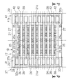
図3は素子チップ18の平面図を概略的に示す。素子チップ18は基板21を備える。基板21の表面(第1面)には素子アレイ22が形成される。素子アレイ22はアレイ状に配置された超音波トランスデューサー素子(以下「素子」という)23で構成される。アレイは複数行複数列のマトリクスで形成される。その他、アレイでは千鳥配置が確立されてもよい。千鳥配置では偶数列の素子23群は奇数列の素子23群に対して行ピッチの2分の1でずらされればよい。奇数列および偶数列の一方の素子数は他方の素子数に比べて1つ少なくてもよい。個々の素子23は圧電素子部を備える。圧電素子部は下部電極24、上部電極25および圧電体膜26で構成される。個々の素子23ごとに下部電極24および上部電極25の間に圧電体膜26が挟み込まれる。
FIG. 3 schematically shows a plan view of the
下部電極24は複数本の第1導電体(電極)24aを有する。第1導電体24aは配列の行方向に相互に平行に延びる。1行の素子23ごとに1本の第1導電体24aが割り当てられる。1本の第1導電体24aは配列の行方向に並ぶ素子23の圧電体膜26に共通に配置される。第1導電体24aの両端は1対の引き出し配線27にそれぞれ接続される。引き出し配線27は配列の列方向に相互に平行に延びる。したがって、全ての第1導電体24aは同一長さを有する。こうしてマトリクス全体の素子23に共通に下部電極24は接続される。
The
上部電極25は複数本の第2導電体(第2電極)25aを有する。第2導電体25aは配列の列方向に相互に平行に延びる。1列の素子23ごとに1本の第2導電体25aが割り当てられる。1本の第2導電体25aは配列の列方向に並ぶ素子23の圧電体膜26に共通に配置される。列ごとに素子23の通電は切り替えられる。こうした通電の切り替えに応じてラインスキャンやセクタースキャンは実現される。1列の素子23は同時に超音波を出力することから、1列の個数すなわち配列の行数は超音波の出力レベルに応じて決定されることができる。行数は例えば10〜15行程度に設定されればよい。図中では省略されて5行が描かれる。配列の列数はスキャンの範囲の広がりに応じて決定されることができる。列数は例えば128列や256列に設定されればよい。図中では省略されて8列が描かれる。
The
基板21の輪郭は、相互に平行な1対の直線29で仕切られて対向する第1辺21aおよび第2辺21bを有する。素子アレイ22の外周と基板21の輪郭との間に広がる周縁領域31には、第1辺21aに沿って第1辺21aに平行に1ラインの第1端子アレイ32aが形成され、第2辺21bに沿って第2辺21bに平行に1ラインの第2端子アレイ32bが形成される。第1端子アレイ32aは1対の下部電極端子33および複数の上部電極端子34で構成される。同様に、第2端子アレイ32bは1対の下部電極端子35および複数の上部電極端子36で構成される。1本の引き出し配線27の両端にそれぞれ下部電極端子33、35は接続される。引き出し配線27および下部電極端子33、35は素子アレイ22を二等分する垂直面で面対称に形成されればよい。1本の第2導電体25aの両端にそれぞれ上部電極端子34、36は接続される。第2導電体25aおよび上部電極端子34、36は素子アレイ22を二等分する垂直面で面対称に形成されればよい。ここでは、基板21の輪郭は矩形に形成される。基板21の輪郭は正方形であってもよく台形であってもよい。
The outline of the
チップユニット17は第1フレキシブルプリント基板(以下「第1フレキ」という)37および第2フレキシブルプリント基板(以下「第2フレキ」という)41を備える。第1フレキ37は基板21に連結される。連結にあたって第1フレキ37は第1端子アレイ32aに覆い被さる。第1フレキ37の第1端37aには下部電極端子33および上部電極端子34に個別に対応して導電線すなわち第1信号線(第2配線)38が形成される。第1信号線38は下部電極端子33および上部電極端子34に個別に向き合わせられ個別に接合される。同様に、第2フレキ41は基板21に連結される。連結にあたって第2フレキ41は第2端子アレイ32bに覆い被さる。第2フレキ41の第1端41aには下部電極端子35および上部電極端子36に個別に対応して導電線すなわち第2信号線(第2配線)42が形成される。第2信号線42は下部電極端子35および上部電極端子36に個別に向き合わせられ個別に接合される。
The
図4に示されるように、個々の素子23は振動膜43を有する。振動膜43の構築にあたって基板21の基体44には個々の素子23ごとに開口45が形成される。開口45は基体44に対してアレイ状に配置される。基体44の表面には可撓膜46が一面に形成される。可撓膜46は、基体44の表面に積層される酸化シリコン(SiO2)層47と、酸化シリコン層47の表面に積層される酸化ジルコニウム(ZrO2)層48とで構成される。可撓膜46は開口45に接する。こうして開口45の輪郭に対応して可撓膜46の一部が振動膜43として機能する。酸化シリコン層47の膜厚は共振周波数に基づき決定されることができる。開口45の輪郭で素子23の輪郭は規定される。開口45のアレイの輪郭で素子アレイ22の輪郭は規定されることができる。
As shown in FIG. 4, each
振動膜43の表面に下部電極24、圧電体膜26および上部電極25が順番に積層される。下部電極24には例えばチタン(Ti)、イリジウム(Ir)、白金(Pt)およびチタン(Ti)の積層膜が用いられることができる。圧電体膜26は例えばジルコン酸チタン酸鉛(PZT)で形成されることができる。上部電極25は例えばイリジウム(Ir)で形成されることができる。下部電極24および上部電極25にはその他の導電材が利用されてもよく、圧電体膜26にはその他の圧電材料が用いられてもよい。ここでは、上部電極25の下で圧電体膜26は完全に下部電極24を覆う。圧電体膜26の働きで上部電極25と下部電極24との間で短絡は回避されることができる。
The
基板21の表面には保護膜49が積層される。保護膜49は例えば全面にわたって基板21の表面に覆い被さる。その結果、素子アレイ22や第1および第2端子アレイ32a、32b、第1および第2フレキ37、41の第1端37a、41aは保護膜49で覆われる。保護膜49には例えばシリコーン樹脂膜が用いられることができる。保護膜49は、素子アレイ22の構造や、第1端子アレイ32aおよび第1フレキ37の接合、第2端子アレイ32bおよび第2フレキ41の接合を保護する。
A
隣接する開口45同士の間には仕切り壁51が区画される。開口45同士は仕切り壁51で仕切られる。開口45同士の間隔は仕切り壁51の厚みtに相当する。開口45の深さは仕切り壁51の高さHに相当する。仕切り壁51の厚みtが縮小されれば、振動膜43の配置密度は高められる。素子チップ18の小型化に寄与することができる。厚みtに比べて仕切り壁51の高さHが大きければ、素子チップ18の曲げ剛性は高められることができる。こうして開口45同士の間隔は開口45の深さよりも小さく設定される。
A
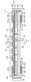
基板21の裏面(第2面)には配線基板52が固定される。配線基板52の表面(第1面)に基板21の裏面が重ねられる。配線基板52は基板21の裏面で開口45を塞ぐ。配線基板52はリジッドな基材を備えることができる。配線基板52は例えばシリコン基板から形成されることができる。基体44の板厚は例えば100μm程度に設定され、配線基板52の板厚は例えば100〜150μm程度に設定される。ここでは、仕切り壁51は配線基板52に結合される。面同士で接合されればよい。
A
配線基板52の裏面(第2面)には第1配線54が形成される。第1配線54は導電材の薄膜で構成されることができる。導電材には例えば銅といった金属材料が用いられることができる。薄膜は配線基板52の裏面に配線パターンを描くことができる。
A
配線基板52の裏面には集積回路(IC)チップ55が実装される。集積回路チップ55は集積回路を構成する。集積回路は第1配線54に接続される。
An integrated circuit (IC)
配線基板52の裏面には外部接続端子56が形成される。外部接続端子56は第1配線54に接続される。外部接続端子56は例えばパッド形状の導電材で構成されることができる。導電材には例えば銅といった金属材料が用いられることができる。外部接続端子56に導電材のバンプ57が結合されてもよい。外部接続端子56は第1配線54経由で集積回路に接続される。ここでは、外部接続端子56にはケーブル14の信号線が結合される。その他、図5に示されるように、外部接続端子56に代えて配線基板52の裏面にはコネクター59が設置されることができる。コネクター59は第1配線54に接続される。コネクター59は筐体16内で受け側のコネクター(図示されず)に結合されることができる。受け側のコネクターにはケーブル14の一端が結合されることができる。
配線基板52には第1フレキ37および第2フレキ41がそれぞれ個別に支持される。支持にあたって第1フレキ37および第2フレキ41は配線基板52の裏面に連結される。配線基板52の裏面には中継端子58が形成される。中継端子58は第1配線54に接続される。中継端子58には第1フレキ37の第2端37bおよび第2フレキ41の第2端41bがそれぞれ覆い被さる。中継端子58には第1信号線38および第2信号線42が個別に接続される。第1信号線38および第2信号線42は例えばはんだや導電接着剤で中継端子58に接合されることができる。こうして第1信号線38および第2信号線42は少なくとも基板21上の素子アレイ22および第1配線54の間で電気的導通を確立する。
The
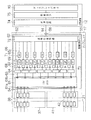
(2)超音波診断装置の回路構成
図6に示されるように、集積回路はマルチプレクサー61および送受信回路62を備える。マルチプレクサー61は素子23側のポート群61aと信号処理側のポート群61bとを備える。素子23側のポート群61aには第1配線54経由で第1信号線38および第2信号線42が接続される。こうしてポート群61aは素子アレイ22に繋がる。ここでは、信号処理側のポート群61bには送受信回路62の規定数の信号線63が接続される。規定数はスキャンにあたって同時に出力される素子23の列数に相当する。マルチプレクサー61は素子23側のポートと信号処理側すなわちケーブル14側のポートとの間で相互接続を管理する。
(2) Circuit Configuration of Ultrasonic Diagnostic Device As shown in FIG. 6, the integrated circuit includes a
送受信回路62は規定数の切り替えスイッチ64を備える。個々の切り替えスイッチ64はそれぞれ個別に対応の信号線63に接続される。送受信回路62は個々の切り替えスイッチ64ごとに送信経路65および受信経路66を備える。切り替えスイッチ64には送信経路65と受信経路66とが並列に接続される。切り替えスイッチ64はマルチプレクサー61に選択的に送信経路65または受信経路66を接続する。送信経路65にはパルサー67が組み込まれる。パルサー67は振動膜43の共振周波数に応じた周波数でパルス信号を出力する。受信経路66にはアンプ68、ローパスフィルター(LPF)69およびアナログデジタル変換器(ADC)71が組み込まれる。個々の素子23の検出信号は増幅されてデジタル信号に変換される。
The transmission /
送受信回路62は駆動/受信回路72を備える。送信経路65および受信経路66は駆動/受信回路72に接続される。駆動/受信回路72はスキャンの形態に応じて同時にパルサー67を制御する。駆動/受信回路72はスキャンの形態に応じて検出信号のデジタル信号を受信する。駆動/受信回路72は制御線73でマルチプレクサー61に接続される。マルチプレクサー61は駆動/受信回路72から供給される制御信号に基づき相互接続の管理を実施する。
The transmission /
装置端末12には処理回路74が組み込まれる。処理回路74は例えば中央演算処理装置(CPU)やメモリーを備えることができる。超音波診断装置11の全体動作は処理回路74の処理に従って制御される。ユーザーから入力される指示に応じて処理回路74は駆動/受信回路72を制御する。処理回路74は素子23の検出信号に応じて画像を生成する。画像は描画データで特定される。
A
装置端末12には描画回路75が組み込まれる。描画回路75は処理回路74に接続される。描画回路75にはディスプレイパネル15が接続される。描画回路75は処理回路74で生成された描画データに応じて駆動信号を生成する。駆動信号はディスプレイパネル15に送り込まれる。その結果、ディスプレイパネル15に画像が映し出される。
A
(3)超音波診断装置の動作
次に超音波診断装置11の動作を簡単に説明する。処理回路74は駆動/受信回路72に超音波の送信および受信を指示する。駆動/受信回路72はマルチプレクサー61に制御信号を供給するとともに個々のパルサー67に駆動信号を供給する。パルサー67は駆動信号の供給に応じてパルス信号を出力する。マルチプレクサー61は制御信号の指示に従ってポート群61bのポートにポート群61aのポートを接続する。パルス信号はポートの選択に応じて下部電極端子33、35および上部電極端子34、36を通じて列ごとに素子23に供給される。パルス信号の供給に応じて振動膜43は振動する。その結果、対象物(例えば人体の内部)に向けて所望の超音波は発せられる。
(3) Operation of Ultrasonic Diagnostic Device Next, the operation of the ultrasonic
超音波の送信後、切り替えスイッチ64は切り替えられる。マルチプレクサー61はポートの接続関係を維持する。切り替えスイッチ64は送信経路65および信号線63の接続に代えて受信経路66および信号線63の接続を確立する。超音波の反射波は振動膜43を振動させる。その結果、素子23から検出信号が出力される。検出信号はデジタル信号に変換されて駆動/受信回路72に送り込まれる。
After transmission of the ultrasonic wave, the
超音波の送信および受信は繰り返される。繰り返しにあたってマルチプレクサー61はポートの接続関係を変更する。その結果、ラインスキャンやセクタースキャンは実現される。スキャンが完了すると、処理回路74は検出信号のデジタル信号に基づき画像を形成する。形成された画像はディスプレイパネル15の画面に表示される。
Transmission and reception of ultrasonic waves are repeated. In the repetition, the
チップユニット17では基板21および配線基板52は第1フレキ37および第2フレキ41で電気的に接続される。第1フレキ37および第2フレキ41は基板21および配線基板52の外側に配置される。基板21と配線基板52との間に接続端子の配置は省略されることができる。その結果、基板21は配線基板52に重ね合わせられることができる。基板21および配線基板52の距離は最大限に縮小される。したがって、集積回路の接続にあたって基板21および配線基板52の厚みは縮小される。
In the
素子チップ18では基板21の裏面に配線基板52が接合される。配線基板52は基板21の強度を補強する。基板21の板厚が例えば100μm程度に設定されても、配線基板52は基板21の破損を防止することができる。その一方で、バルク型の超音波トランスデューサー素子で素子アレイが構成される場合には、基板の板厚は500μm〜数mm程度に設定される。たとえ配線基板52が接合されても、素子チップ18の厚みは、バルク型の超音波トランスデューサー素子で素子アレイが構成される場合に比べて確実に縮小されることができる。加えて、振動膜43の音響インピーダンスはバルク型の超音波トランスデューサー素子に比べて人体のそれに近いことから、素子チップ18ではバルク型の超音波トランスデューサー素子に比べて音響インピーダンスの整合層が省略されることができる。こういった整合層の省略は素子チップ18の薄型化にさらに寄与することができる。
In the
さらに、素子チップ18では仕切り壁51は配線基板52に結合される。仕切り壁51の剛性は高められることができる。その結果、仕切り壁51の振動(残響振動)は抑制されることができる。素子23の振動特性は安定化することができる。その一方で、仕切り壁51の厚みtが高さHより小さいと、断面のアスペクト比の関係で、仕切り壁51の曲げ剛性は素子チップ18の面内方向に弱まる。仕切り壁51が配線基板52に結合されないと、仕切り壁51は素子チップ18の面内方向に振動しやすい。いわゆるクロストークが発生してしまう。
Further, in the
素子チップ18には集積回路が組み込まれる。集積回路チップ55は、素子アレイ22に接続される導電線の本数すなわち下部電極端子33、35および上部電極端子34、36の個数よりも少ない本数の入出力端子で外部接続端子56に接続されることができる。集積回路チップ55の入出力端子の端子数は下部電極端子33、35および上部電極端子34、36の個数よりも減少する。その結果、素子チップ18に接続されるケーブル14やコネクターのサイズは縮小されることができる。素子チップ18は従来に比べて狭小な空間に収容されることができる。
An integrated circuit is incorporated in the
特に、集積回路チップ55にはマルチプレクサー61が組み込まれる。マルチプレクサー61は、下部電極端子33、35および上部電極端子34、36に接続されるポート群61aと、下部電極端子33、35および上部電極端子34、36の個数よりも少ない本数の信号処理側のポート群61bとの間で接続関係を管理する。したがって、マルチプレクサー61は、素子チップ18に接続されるケーブル14やコネクターのサイズの縮小に大いに貢献する。
In particular, a
加えて、集積回路チップ55にはパルサー67が組み込まれる。素子23とパルサー67との間で距離は短縮される。したがって、素子23に供給される共振信号のS/N比は高められることができる。また、集積回路チップ55にはアナログデジタル変換器71がさらに組み込まれる。素子23とアナログデジタル変換器71との間で距離は短縮される。したがって、素子33から出力される検出信号のS/N比は高められることができる。
In addition, a pulser 67 is incorporated in the
素子チップ18では配線基板52の裏面に外部接続端子56が形成される。こうしてチップユニット17は1つのユニットとして取り扱われることができる。外部接続端子56で簡単に実装されることができる。しかも、外部接続端子56は基板21の裏側に引き回されることから、基板21を含む二次元平面に沿って配線基板52の広がりは抑制されることができる。チップユニット17の小型化に貢献することができる。
In the
素子チップ18では下部電極24は第1導電体24aを有する。第1導電体24aの両端はそれぞれ引き出し配線27に接続される。引き出し配線27には下部電極端子33、35から共振信号が入力される。こうして第1導電体24aには両端から共振信号が供給されることから、電圧降下の影響はできるだけ低減されることができる。同様に、上部電極25は第2導電体25aを有する。第2導電体25aの両端はそれぞれ上部電極端子34、36に接続される。したがって、第2導電体25aには両端の上部電極端子34、36から共振信号が供給される。電圧降下の影響はできるだけ抑制されることができる。
In the
(4)第2実施形態に係るチップユニットの構成
図7は第2実施形態に係るチップユニット17の構成を概略的に示す。超音波診断装置11は前述の素子チップ18に代えて素子チップ18aを利用することができる。この第2実施形態では、第1実施形態の集積回路チップ55に代わって、配線基板52の裏面に形成されるモノリシック集積回路81で前述の集積回路が構成される。モノリシック集積回路81は配線基板52の裏面に形成されることから素子チップ18aの小型化に貢献することができる。他の構成は前述の第1実施形態と同様に構成されることができる。例えば図7では第1配線は図示されていないが、第1実施形態と同様に配線基板52の裏面に第1配線が形成され、モノリシック集積回路81、外部接続端子56、中継端子58が第1配線に接続される。その他、前述の第1実施形態と均等な構成や構造には同一の参照符号が付され、重複する説明は割愛される。
(4) Configuration of Chip Unit According to Second Embodiment FIG. 7 schematically shows the configuration of the
(5)第3実施形態に係るチップユニットの構成
図8は第3実施形態に係るチップユニット17の構成を概略的に示す。超音波診断装置11は前述の素子チップ18に代えて素子チップ18bを利用することができる。この第3実施形態では集積回路チップ55は第1フレキ37および(または)第2フレキ41に実装される。第1フレキ37上で集積回路チップ55は第1フレキ37の導電線に接続される。第2フレキ41上で集積回路チップ55は第2フレキ41の導電線に接続される。集積回路チップ55は、基板21を含む二次元平面に沿って広がらないことから、素子チップ18bの小型化に貢献することができる。他の構成は前述の第1実施形態および第2実施形態と同様に構成されることができる。例えば図8では第1配線は図示されていないが、第1実施形態と同様に配線基板52の裏面に第1配線が形成され、モノリシック集積回路81、外部接続端子56、中継端子58が第1配線に接続される。その他、前述の第1および第2実施形態と均等な構成や構造には同一の参照符号が付され、重複する説明は割愛される。
(5) Configuration of Chip Unit According to Third Embodiment FIG. 8 schematically shows the configuration of the
(6)第4実施形態に係るチップユニットの構成
図9は第4実施形態に係るチップユニット17の構成を概略的に示す。超音波診断装置11は前述の素子チップ18に代えて素子チップ18cを利用することができる。この第4実施形態では前述の配線基板52に代えて配線基板82が用いられる。配線基板82は表面で基板21を受け止める。配線基板82の裏面は平面に形成される。配線基板82の表面に第1配線83が形成される。第1配線83の形成にあたって配線基板82は基板21の輪郭よりも外側に広がる。第1配線83は導電材の薄膜で構成されることができる。導電材には例えば銅といった金属材料が用いられることができる。薄膜は配線基板82の表面に配線パターンを描くことができる。
(6) Configuration of Chip Unit According to Fourth Embodiment FIG. 9 schematically shows the configuration of the
配線基板82には第1フレキ37および第2フレキ41がそれぞれ個別に支持される。支持にあたって第1フレキ37および第2フレキ41は配線基板82の表面に連結される。配線基板82の表面には中継端子84が形成される。中継端子84は第1配線83に繋がる。中継端子84には第1フレキ37の第2端37bおよび第2フレキ41の第2端41bがそれぞれ覆い被さる。中継端子84には第1信号線38および第2信号線42が個別に接続される。第1信号線38および第2信号線42は例えばはんだや導電接着剤で中継端子84に接合されることができる。こうして第1信号線38および第2信号線42は少なくとも基板21上の素子アレイ22および第1配線83の間で電気的導通を確立する。配線基板82の表面には集積回路チップ55が実装される。集積回路は第1配線83に繋がる。
The first
配線基板82の表面には外部接続端子85が形成される。外部接続端子85は第1配線83に接続される。外部接続端子85は例えばパッド形状の導電材で構成されることができる。導電材には例えば銅といった金属材料が用いられることができる。外部接続端子85は例えばワイヤーボンディング86でケーブル14の信号線に結合されることができる。外部接続端子85は第1配線83経由で集積回路に接続される。
こうした素子チップ18cの採用によれば、外部接続端子85の形成作業、および、外部接続端子85および第1配線83の接続作業はいずれも配線基板82の表面で実施されることができ、製造工程の複雑化は回避されることができる。他の構成は前述の第1〜第3実施形態と同様に構成されることができる。前述の第1〜第3実施形態と均等な構成や構造には同一の参照符号が付され、重複する説明は割愛される。
According to the adoption of such an
なお、上記のように本実施形態について詳細に説明したが、本発明の新規事項および効果から実体的に逸脱しない多くの変形が可能であることは当業者には容易に理解できるであろう。したがって、このような変形例はすべて本発明の範囲に含まれる。例えば、明細書または図面において、少なくとも一度、より広義または同義な異なる用語とともに記載された用語は、明細書または図面のいかなる箇所においても、その異なる用語に置き換えられることができる。また、超音波診断装置11、超音波プローブ13、チップユニット17、超音波トランスデューサー素子23、集積回路、処理回路74等の構成および動作も本実施形態で説明したものに限定されず、種々の変形が可能である。
Although the present embodiment has been described in detail as described above, it will be easily understood by those skilled in the art that many modifications can be made without departing from the novel matters and effects of the present invention. Therefore, all such modifications are included in the scope of the present invention. For example, a term described with a different term having a broader meaning or the same meaning at least once in the specification or the drawings can be replaced with the different term in any part of the specification or the drawings. In addition, the configurations and operations of the ultrasonic
11 超音波診断装置(電子機器)、13 プローブ(超音波プローブ)、16 筐体、17 超音波トランスデューサー装置(超音波トランスデューサー素子チップユニット)、18 超音波トランスデューサー素子チップ、21 基板、23 超音波トランスデューサー素子、38 第2配線(第1信号線)、42 第2配線(第2信号線)、45 開口、52 配線基板、54 第1配線、55 集積回路(集積回路チップ)、56 外部接続端子、61 マルチプレクサー、67 パルサー、71 アナログデジタル変換器、74 処理回路、81 集積回路(モノリシック集積回路)、82 配線基板、83 第1配線、85 外部接続端子。
DESCRIPTION OF
Claims (18)
前記複数の開口に設けられ、行方向及び列方向に配列される超音波トランスデューサー素子と、
前記超音波トランスデューサー素子が設けられる前記基板の第1面とは反対側の前記基板の第2面に対向配置され、第1配線を有する配線基板と、
前記基板および前記配線基板に接続されて、前記超音波トランスデューサー素子および前記第1配線を相互に電気的に接続する第2配線を有する配線部材と、
を備え、
前記基板は、
前記行方向に並ぶ前記超音波トランスデューサー素子に共通に延びて、前記行方向に並ぶ前記超音波トランスデューサー素子に接続される1本の第1電極と、
前記第1電極の両端にそれぞれ個別に接続される第1電極端子と、
前記列方向に並ぶ前記超音波トランスデューサー素子に共通に延びて、前記列方向に並ぶ前記超音波トランスデューサー素子に接続される1本の第2電極と、
前記第2電極の両端にそれぞれ個別に接続される第2電極端子と、
を備えることを特徴とする超音波トランスデューサー装置。 A substrate having a plurality of openings arranged in an array; and
Provided in the plurality of openings, and the ultrasonic transducer element that is arranged in the row direction and a column direction,
A wiring substrate having a first wiring disposed opposite to the second surface of the substrate opposite to the first surface of the substrate on which the ultrasonic transducer element is provided;
A wiring member connected to the substrate and the wiring substrate and having a second wiring that electrically connects the ultrasonic transducer element and the first wiring;
Equipped with a,
The substrate is
A first electrode extending in common to the ultrasonic transducer elements arranged in the row direction and connected to the ultrasonic transducer elements arranged in the row direction;
First electrode terminals individually connected to both ends of the first electrode;
A second electrode extending in common to the ultrasonic transducer elements arranged in the column direction and connected to the ultrasonic transducer elements arranged in the column direction;
A second electrode terminal individually connected to both ends of the second electrode;
An ultrasonic transducer device comprising:
前記配線部材は、前記第2配線を含む導電線を有するフレキシブルプリント基板であり、
前記集積回路は、前記フレキシブルプリント基板に実装され、かつ前記導電線に接続されている集積回路チップを含むことを特徴とする超音波トランスデューサー装置。 The ultrasonic transducer device according to claim 4,
The wiring member is a flexible printed board having a conductive line including the second wiring,
The ultrasonic transducer device, wherein the integrated circuit includes an integrated circuit chip mounted on the flexible printed board and connected to the conductive wire.
前記開口に設けられる超音波トランスデューサー素子と、
前記超音波トランスデューサー素子が設けられる前記基板の第1面とは反対側の前記基板の第2面に対向配置され、第1配線を有する配線基板と、
前記基板および前記配線基板に接続されて、前記超音波トランスデューサー素子および前記第1配線を相互に電気的に接続する第2配線を有する配線部材と、を備える超音波トランスデューサー装置を含み、
前記基板は、
前記行方向に並ぶ前記超音波トランスデューサー素子に共通に延びて、前記行方向に並ぶ前記超音波トランスデューサー素子に接続される1本の第1電極と、
前記第1電極の両端にそれぞれ個別に接続される第1電極端子と、
前記列方向に並ぶ前記超音波トランスデューサー素子に共通に延びて、前記列方向に並ぶ前記超音波トランスデューサー素子に接続される1本の第2電極と、
前記第2電極の両端にそれぞれ個別に接続される第2電極端子と、
を備えることを特徴とする電子機器。 A substrate having a plurality of openings arranged in an array; and
An ultrasonic transducer element provided in the opening;
A wiring substrate having a first wiring disposed opposite to the second surface of the substrate opposite to the first surface of the substrate on which the ultrasonic transducer element is provided;
The substrate and connected to the wiring board, seen including a wiring member, the ultrasonic transducer device comprising a having a second wiring connecting the ultrasonic transducer element and the first wire to each other electrically,
The substrate is
A first electrode extending in common to the ultrasonic transducer elements arranged in the row direction and connected to the ultrasonic transducer elements arranged in the row direction;
First electrode terminals individually connected to both ends of the first electrode;
A second electrode extending in common to the ultrasonic transducer elements arranged in the column direction and connected to the ultrasonic transducer elements arranged in the column direction;
A second electrode terminal individually connected to both ends of the second electrode;
An electronic apparatus comprising: a.
前記開口に設けられる超音波トランスデューサー素子と、
前記超音波トランスデューサー素子が設けられる前記基板の第1面とは反対側の前記基板の第2面に対向配置され、第1配線を有する配線基板と、
前記基板および前記配線基板に接続されて、前記超音波トランスデューサー素子および前記第1配線を相互に電気的に接続する第2配線を有する配線部材と、を備える超音波トランスデューサー装置を含み、
前記基板は、
前記行方向に並ぶ前記超音波トランスデューサー素子に共通に延びて、前記行方向に並ぶ前記超音波トランスデューサー素子に接続される1本の第1電極と、
前記第1電極の両端にそれぞれ個別に接続される第1電極端子と、
前記列方向に並ぶ前記超音波トランスデューサー素子に共通に延びて、前記列方向に並ぶ前記超音波トランスデューサー素子に接続される1本の第2電極と、
前記第2電極の両端にそれぞれ個別に接続される第2電極端子と、
を備えることを特徴とする超音波診断装置。
A substrate having a plurality of openings arranged in an array; and
An ultrasonic transducer element provided in the opening;
A wiring substrate having a first wiring disposed opposite to the second surface of the substrate opposite to the first surface of the substrate on which the ultrasonic transducer element is provided;
The substrate and connected to the wiring board, seen including a wiring member, the ultrasonic transducer device comprising a having a second wiring connecting the ultrasonic transducer element and the first wire to each other electrically,
The substrate is
A first electrode extending in common to the ultrasonic transducer elements arranged in the row direction and connected to the ultrasonic transducer elements arranged in the row direction;
First electrode terminals individually connected to both ends of the first electrode;
A second electrode extending in common to the ultrasonic transducer elements arranged in the column direction and connected to the ultrasonic transducer elements arranged in the column direction;
A second electrode terminal individually connected to both ends of the second electrode;
An ultrasonic diagnostic apparatus comprising:
Priority Applications (5)
| Application Number | Priority Date | Filing Date | Title |
|---|---|---|---|
| JP2012038401A JP5990929B2 (en) | 2012-02-24 | 2012-02-24 | Ultrasonic transducer device and probe, electronic device and ultrasonic diagnostic device |
| CN201310052062.2A CN103284755B (en) | 2012-02-24 | 2013-02-17 | Ultrasound transducer apparatus, detector, electronic equipment and diagnostic ultrasound equipment |
| CN201610698500.6A CN106236139B (en) | 2012-02-24 | 2013-02-17 | Ultrasound transducer apparatus, detector, electronic equipment and diagnostic ultrasound equipment |
| US13/770,153 US9197331B2 (en) | 2012-02-24 | 2013-02-19 | Ultrasonic transducer device, probe, electronic instrument, and ultrasonic diagnostic device |
| US14/929,875 US9692524B2 (en) | 2012-02-24 | 2015-11-02 | Ultrasonic transducer device, probe, electronic instrument, and ultrasonic diagnostic device |
Applications Claiming Priority (1)
| Application Number | Priority Date | Filing Date | Title |
|---|---|---|---|
| JP2012038401A JP5990929B2 (en) | 2012-02-24 | 2012-02-24 | Ultrasonic transducer device and probe, electronic device and ultrasonic diagnostic device |
Publications (3)
| Publication Number | Publication Date |
|---|---|
| JP2013175878A JP2013175878A (en) | 2013-09-05 |
| JP2013175878A5 JP2013175878A5 (en) | 2015-04-09 |
| JP5990929B2 true JP5990929B2 (en) | 2016-09-14 |
Family
ID=49002734
Family Applications (1)
| Application Number | Title | Priority Date | Filing Date |
|---|---|---|---|
| JP2012038401A Active JP5990929B2 (en) | 2012-02-24 | 2012-02-24 | Ultrasonic transducer device and probe, electronic device and ultrasonic diagnostic device |
Country Status (3)
| Country | Link |
|---|---|
| US (2) | US9197331B2 (en) |
| JP (1) | JP5990929B2 (en) |
| CN (2) | CN106236139B (en) |
Families Citing this family (17)
| Publication number | Priority date | Publication date | Assignee | Title |
|---|---|---|---|---|
| JP5990929B2 (en) * | 2012-02-24 | 2016-09-14 | セイコーエプソン株式会社 | Ultrasonic transducer device and probe, electronic device and ultrasonic diagnostic device |
| KR102126033B1 (en) * | 2013-10-23 | 2020-06-23 | 삼성전자주식회사 | Ultrasonic transducer and ultrasonic diagnostic equipment including the same |
| JP6281262B2 (en) * | 2013-11-29 | 2018-02-21 | セイコーエプソン株式会社 | Ultrasonic device and probe, electronic apparatus and ultrasonic imaging apparatus |
| JP6468426B2 (en) * | 2014-03-10 | 2019-02-13 | セイコーエプソン株式会社 | Ultrasonic sensor |
| EP3140049B1 (en) * | 2014-05-06 | 2018-08-01 | Koninklijke Philips N.V. | Ultrasonic transducer chip assembly, ultrasound probe, ultrasonic imaging system and ultrasound assembly and probe manufacturing methods |
| US10130339B2 (en) * | 2014-06-30 | 2018-11-20 | Seiko Epson Corporation | Ultrasound sensor and method of manufacturing thereof |
| JP6299511B2 (en) * | 2014-07-31 | 2018-03-28 | セイコーエプソン株式会社 | Ultrasonic device and probe and electronic equipment |
| JP2016033970A (en) * | 2014-07-31 | 2016-03-10 | セイコーエプソン株式会社 | Ultrasonic device and method for manufacturing the same, and probe and electronic equipment |
| JP6398454B2 (en) * | 2014-08-13 | 2018-10-03 | セイコーエプソン株式会社 | Piezoelectric drive device, robot, and drive method thereof |
| JP6402983B2 (en) * | 2014-08-29 | 2018-10-10 | セイコーエプソン株式会社 | Ultrasonic device, method for manufacturing ultrasonic device, ultrasonic probe, ultrasonic measuring device, electronic equipment |
| JP2016086956A (en) * | 2014-10-31 | 2016-05-23 | セイコーエプソン株式会社 | Ultrasonic probe, electronic apparatus, and ultrasonogram device |
| KR20160069293A (en) * | 2014-12-08 | 2016-06-16 | 삼성전자주식회사 | Probe, Ultrasound Imaging Apparatus, and Controlling Method of the Ultrasound Imaging Apparatus |
| USD831834S1 (en) * | 2015-12-04 | 2018-10-23 | Sonotec Ultraschallsensorik Halle Gmbh | Ultrasonic probe |
| EP3459465A4 (en) * | 2016-05-20 | 2020-01-15 | Olympus Corporation | Ultrasonic transducer module, ultrasonic endoscope, and method for manufacturing ultrasonic transducer module |
| CN106332448B (en) * | 2016-08-06 | 2019-04-12 | 业成科技(成都)有限公司 | Ultrasonic sensor and electronic device with the ultrasonic sensor |
| JP6828389B2 (en) * | 2016-11-16 | 2021-02-10 | セイコーエプソン株式会社 | Ultrasonic Transducer Devices, Ultrasonic Probes and Ultrasonic Devices |
| JP6922300B2 (en) * | 2017-03-22 | 2021-08-18 | セイコーエプソン株式会社 | Ultrasonic device unit, ultrasonic probe, and ultrasonic device |
Family Cites Families (49)
| Publication number | Priority date | Publication date | Assignee | Title |
|---|---|---|---|---|
| JPH0730136Y2 (en) * | 1987-06-29 | 1995-07-12 | タマパック株式会社 | Oscillator |
| JP3940683B2 (en) * | 2003-02-24 | 2007-07-04 | 株式会社東芝 | Ultrasonic probe and manufacturing method thereof |
| US7491172B2 (en) | 2004-01-13 | 2009-02-17 | General Electric Company | Connection apparatus and method for controlling an ultrasound probe |
| US7431698B2 (en) | 2004-01-13 | 2008-10-07 | Ge Medical Systems Global Technology Company, Llc | Apparatus and method for controlling an ultrasound probe |
| US7867168B2 (en) * | 2004-08-24 | 2011-01-11 | Sonosite, Inc. | Ultrasonic transducer having distributed weight properties |
| EP1810619B1 (en) | 2004-10-27 | 2011-09-14 | Olympus Corporation | Capacitive ultrasonic transducer and endo cavity ultrasonic diagnosis system using the same |
| JP4624763B2 (en) | 2004-10-27 | 2011-02-02 | オリンパス株式会社 | Capacitive ultrasonic transducer and manufacturing method thereof |
| JP4744849B2 (en) | 2004-11-11 | 2011-08-10 | 株式会社東芝 | Semiconductor device |
| US8047995B2 (en) * | 2007-08-28 | 2011-11-01 | Olympus Medical Systems Corp. | Ultrasonic transducer, method of manufacturing ultrasonic transducer, ultrasonic diagnostic apparatus, and ultrasonic microscope |
| JP4774393B2 (en) * | 2007-08-28 | 2011-09-14 | オリンパスメディカルシステムズ株式会社 | Ultrasonic transducer, ultrasonic diagnostic apparatus and ultrasonic microscope |
| JP5129011B2 (en) * | 2008-04-24 | 2013-01-23 | シャープ株式会社 | Sensor element, analysis chip, and analysis device using nanostructures |
| WO2010044312A1 (en) * | 2008-10-17 | 2010-04-22 | コニカミノルタエムジー株式会社 | Array-type ultrasonic vibrator |
| JP5206432B2 (en) | 2009-01-13 | 2013-06-12 | セイコーエプソン株式会社 | Detection device and electronic device |
| JP5499479B2 (en) | 2009-01-13 | 2014-05-21 | セイコーエプソン株式会社 | Electronics |
| JP5206433B2 (en) | 2009-01-13 | 2013-06-12 | セイコーエプソン株式会社 | Input device and input method |
| JP5177033B2 (en) | 2009-03-18 | 2013-04-03 | セイコーエプソン株式会社 | Input device and electronic device |
| JP2010244119A (en) | 2009-04-01 | 2010-10-28 | Seiko Epson Corp | Input auxiliary device, and input device |
| US8286488B2 (en) * | 2009-05-01 | 2012-10-16 | General Electric Company | Apparatus and system for measuring material thickness |
| JP5332060B2 (en) * | 2009-05-09 | 2013-11-06 | 本多電子株式会社 | Ultrasonic diagnostic equipment |
| US20110060225A1 (en) * | 2009-09-09 | 2011-03-10 | General Electric Company | Ultrasound probe with integrated pulsers |
| JP2011082624A (en) | 2009-10-02 | 2011-04-21 | Asahi Kasei Electronics Co Ltd | Proximity ultrasonic sensor |
| JP5671876B2 (en) | 2009-11-16 | 2015-02-18 | セイコーエプソン株式会社 | Ultrasonic transducer, ultrasonic sensor, method for manufacturing ultrasonic transducer, and method for manufacturing ultrasonic sensor |
| JP5754129B2 (en) * | 2010-03-11 | 2015-07-29 | セイコーエプソン株式会社 | Piezoelectric element, piezoelectric sensor, electronic device, and method of manufacturing piezoelectric element |
| JP2013527702A (en) * | 2010-04-29 | 2013-06-27 | リサーチ・トライアングル・インスティチュート | Method and associated apparatus for forming a connection with a micromachined ultrasonic transducer |
| JP5435802B2 (en) | 2010-06-25 | 2014-03-05 | 富士フイルム株式会社 | Piezoelectric thin film element, ultrasonic sensor using the same, and manufacturing method thereof |
| JP5678670B2 (en) * | 2011-01-06 | 2015-03-04 | セイコーエプソン株式会社 | Ultrasonic sensor, tactile sensor, and gripping device |
| JP5708214B2 (en) * | 2011-03-28 | 2015-04-30 | セイコーエプソン株式会社 | Pressure sensor, sensor array, sensor array manufacturing method, and gripping device |
| JP5834657B2 (en) * | 2011-09-12 | 2015-12-24 | セイコーエプソン株式会社 | Ultrasonic probe and ultrasonic diagnostic imaging apparatus |
| JP5990929B2 (en) * | 2012-02-24 | 2016-09-14 | セイコーエプソン株式会社 | Ultrasonic transducer device and probe, electronic device and ultrasonic diagnostic device |
| JP5978649B2 (en) * | 2012-02-24 | 2016-08-24 | セイコーエプソン株式会社 | Ultrasonic transducer element chip, probe head and probe, electronic device and ultrasonic diagnostic apparatus |
| JP6019671B2 (en) * | 2012-03-30 | 2016-11-02 | セイコーエプソン株式会社 | Ultrasonic probe, electronic device, and ultrasonic diagnostic apparatus |
| US20130342810A1 (en) * | 2012-06-04 | 2013-12-26 | Seiko Epson Corporation | Eyeball biological information collection device and method for collecting eyeball biological information |
| JP6089499B2 (en) * | 2012-08-28 | 2017-03-08 | セイコーエプソン株式会社 | Ultrasonic transducer device and probe, electronic device and ultrasonic diagnostic device |
| JP6011235B2 (en) * | 2012-10-17 | 2016-10-19 | セイコーエプソン株式会社 | Ultrasonic measuring device, probe head, ultrasonic probe, electronic device and ultrasonic diagnostic device |
| JP6186696B2 (en) * | 2012-10-25 | 2017-08-30 | セイコーエプソン株式会社 | Ultrasonic measuring device, head unit, probe and diagnostic device |
| JP6205704B2 (en) * | 2012-10-25 | 2017-10-04 | セイコーエプソン株式会社 | Ultrasonic measuring device, head unit, probe and diagnostic device |
| JP2014083281A (en) * | 2012-10-25 | 2014-05-12 | Seiko Epson Corp | Ultrasonic measuring device, head unit, probe, and diagnostic system |
| JP2014083283A (en) * | 2012-10-25 | 2014-05-12 | Seiko Epson Corp | Ultrasonic measuring device, head unit, probe, and diagnostic system |
| JP6102284B2 (en) * | 2013-01-29 | 2017-03-29 | セイコーエプソン株式会社 | Ultrasonic measuring device, ultrasonic head unit, ultrasonic probe, and ultrasonic imaging device |
| JP6160120B2 (en) * | 2013-02-28 | 2017-07-12 | セイコーエプソン株式会社 | Ultrasonic transducer device, ultrasonic measurement device, head unit, probe, and ultrasonic imaging device |
| JP2014175577A (en) * | 2013-03-12 | 2014-09-22 | Seiko Epson Corp | Piezoelectric element, liquid ejecting head, liquid ejector, ultrasonic transducer and ultrasonic device |
| JP6164405B2 (en) * | 2013-03-28 | 2017-07-19 | セイコーエプソン株式会社 | Piezoelectric element module, ultrasonic transducer, ultrasonic device, liquid ejecting head, liquid ejecting apparatus, and method of manufacturing piezoelectric element module |
| JP2015023994A (en) * | 2013-07-26 | 2015-02-05 | セイコーエプソン株式会社 | Ultrasonic measurement device, ultrasonic head unit, ultrasonic probe, and ultrasonic imaging device |
| JP2015023995A (en) * | 2013-07-26 | 2015-02-05 | セイコーエプソン株式会社 | Ultrasonic measurement device, ultrasonic head unit, ultrasonic probe and ultrasonic imaging device |
| JP6183599B2 (en) * | 2013-08-20 | 2017-08-23 | セイコーエプソン株式会社 | Piezoelectric element manufacturing method, liquid jet head manufacturing method, and ultrasonic transducer manufacturing method |
| JP6248535B2 (en) * | 2013-10-23 | 2017-12-20 | セイコーエプソン株式会社 | Ultrasonic device, ultrasonic probe head, ultrasonic probe, electronic apparatus, ultrasonic imaging apparatus, and method of manufacturing ultrasonic device |
| JP6229431B2 (en) * | 2013-10-28 | 2017-11-15 | セイコーエプソン株式会社 | Ultrasonic device, ultrasonic probe head, ultrasonic probe, electronic device and ultrasonic imaging apparatus |
| JP6252130B2 (en) * | 2013-11-20 | 2017-12-27 | セイコーエプソン株式会社 | Ultrasonic device, manufacturing method thereof, electronic apparatus, and ultrasonic imaging apparatus |
| JP6281262B2 (en) * | 2013-11-29 | 2018-02-21 | セイコーエプソン株式会社 | Ultrasonic device and probe, electronic apparatus and ultrasonic imaging apparatus |
-
2012
- 2012-02-24 JP JP2012038401A patent/JP5990929B2/en active Active
-
2013
- 2013-02-17 CN CN201610698500.6A patent/CN106236139B/en active Active
- 2013-02-17 CN CN201310052062.2A patent/CN103284755B/en active Active
- 2013-02-19 US US13/770,153 patent/US9197331B2/en active Active
-
2015
- 2015-11-02 US US14/929,875 patent/US9692524B2/en active Active
Also Published As
| Publication number | Publication date |
|---|---|
| CN103284755A (en) | 2013-09-11 |
| US20160056901A1 (en) | 2016-02-25 |
| US9692524B2 (en) | 2017-06-27 |
| US9197331B2 (en) | 2015-11-24 |
| US20130223192A1 (en) | 2013-08-29 |
| JP2013175878A (en) | 2013-09-05 |
| CN106236139A (en) | 2016-12-21 |
| CN106236139B (en) | 2019-08-16 |
| CN103284755B (en) | 2016-08-24 |
Similar Documents
| Publication | Publication Date | Title |
|---|---|---|
| JP5990929B2 (en) | Ultrasonic transducer device and probe, electronic device and ultrasonic diagnostic device | |
| JP5990930B2 (en) | Ultrasonic transducer element chip and probe, electronic device and ultrasonic diagnostic apparatus | |
| JP6078994B2 (en) | Ultrasonic transducer element unit, probe, probe head, electronic device, and ultrasonic diagnostic apparatus | |
| US20140066778A1 (en) | Ultrasonic transducer device, probe, electronic instrument, and ultrasonic diagnostic device | |
| JP6102075B2 (en) | Ultrasonic transducer element chip and probe, electronic device and ultrasonic diagnostic apparatus | |
| JP6047936B2 (en) | Ultrasonic transducer element package, probe, probe head, electronic device, ultrasonic diagnostic apparatus, and method of manufacturing ultrasonic transducer element package | |
| JP5978649B2 (en) | Ultrasonic transducer element chip, probe head and probe, electronic device and ultrasonic diagnostic apparatus | |
| JP5900107B2 (en) | Ultrasonic transducer element chip and probe, electronic device and ultrasonic diagnostic apparatus | |
| JP6136464B2 (en) | ULTRASONIC TRANSDUCER DEVICE AND PROBE, ELECTRONIC DEVICE, AND ULTRASONIC IMAGING DEVICE | |
| JP2015195351A (en) | Piezoelectric element, piezoelectric device and probe, and electronic device and ultrasonic image device | |
| JP6252279B2 (en) | ULTRASONIC TRANSDUCER DEVICE AND PROBE, ELECTRONIC DEVICE, AND ULTRASONIC IMAGING DEVICE | |
| JP6221582B2 (en) | Ultrasonic device and probe, electronic apparatus and ultrasonic imaging apparatus | |
| JP6273743B2 (en) | Ultrasonic device and probe, electronic apparatus and ultrasonic imaging apparatus | |
| JP2016086956A (en) | Ultrasonic probe, electronic apparatus, and ultrasonogram device | |
| JP2014195495A (en) | Ultrasonic transducer device, probe, electronic device, and ultrasonic image device | |
| JP2015160104A (en) | Ultrasonic device unit, probe, electronic device and ultrasonic image apparatus | |
| JP6365726B2 (en) | Ultrasonic transducer device and electronic equipment | |
| JP2017000792A (en) | Ultrasonic transducer element chip, probe, electronic device, and ultrasonic diagnostic device | |
| JP6311815B2 (en) | Ultrasonic transducer element chip and probe, electronic device and ultrasonic diagnostic apparatus | |
| JP6222259B2 (en) | Ultrasonic transducer element chip and probe, electronic device and ultrasonic diagnostic apparatus |
Legal Events
| Date | Code | Title | Description |
|---|---|---|---|
| A521 | Request for written amendment filed |
Free format text: JAPANESE INTERMEDIATE CODE: A523 Effective date: 20150224 |
|
| A621 | Written request for application examination |
Free format text: JAPANESE INTERMEDIATE CODE: A621 Effective date: 20150224 |
|
| A977 | Report on retrieval |
Free format text: JAPANESE INTERMEDIATE CODE: A971007 Effective date: 20151217 |
|
| A131 | Notification of reasons for refusal |
Free format text: JAPANESE INTERMEDIATE CODE: A131 Effective date: 20160105 |
|
| A521 | Request for written amendment filed |
Free format text: JAPANESE INTERMEDIATE CODE: A523 Effective date: 20160307 |
|
| TRDD | Decision of grant or rejection written | ||
| A01 | Written decision to grant a patent or to grant a registration (utility model) |
Free format text: JAPANESE INTERMEDIATE CODE: A01 Effective date: 20160719 |
|
| A61 | First payment of annual fees (during grant procedure) |
Free format text: JAPANESE INTERMEDIATE CODE: A61 Effective date: 20160801 |
|
| R150 | Certificate of patent or registration of utility model |
Ref document number: 5990929 Country of ref document: JP Free format text: JAPANESE INTERMEDIATE CODE: R150 |