JP6089499B2 - Ultrasonic transducer device and probe, electronic device and ultrasonic diagnostic device - Google Patents
Ultrasonic transducer device and probe, electronic device and ultrasonic diagnostic device Download PDFInfo
- Publication number
- JP6089499B2 JP6089499B2 JP2012187465A JP2012187465A JP6089499B2 JP 6089499 B2 JP6089499 B2 JP 6089499B2 JP 2012187465 A JP2012187465 A JP 2012187465A JP 2012187465 A JP2012187465 A JP 2012187465A JP 6089499 B2 JP6089499 B2 JP 6089499B2
- Authority
- JP
- Japan
- Prior art keywords
- piezoelectric element
- ultrasonic transducer
- transducer device
- opening
- substrate
- Prior art date
- Legal status (The legal status is an assumption and is not a legal conclusion. Google has not performed a legal analysis and makes no representation as to the accuracy of the status listed.)
- Active
Links
- 239000000523 sample Substances 0.000 title claims description 25
- 230000035945 sensitivity Effects 0.000 claims description 70
- 239000000758 substrate Substances 0.000 claims description 59
- 238000001514 detection method Methods 0.000 claims description 53
- 230000010287 polarization Effects 0.000 claims description 34
- 238000005192 partition Methods 0.000 claims description 22
- 238000000034 method Methods 0.000 claims description 12
- 239000012528 membrane Substances 0.000 claims description 11
- 230000008569 process Effects 0.000 claims description 9
- 239000011159 matrix material Substances 0.000 claims description 7
- 239000004020 conductor Substances 0.000 description 73
- 230000005540 biological transmission Effects 0.000 description 30
- 230000007423 decrease Effects 0.000 description 24
- 230000004044 response Effects 0.000 description 20
- XUIMIQQOPSSXEZ-UHFFFAOYSA-N Silicon Chemical compound [Si] XUIMIQQOPSSXEZ-UHFFFAOYSA-N 0.000 description 12
- 229910052710 silicon Inorganic materials 0.000 description 12
- 239000010703 silicon Substances 0.000 description 12
- 230000003014 reinforcing effect Effects 0.000 description 9
- 239000000463 material Substances 0.000 description 8
- VYPSYNLAJGMNEJ-UHFFFAOYSA-N Silicium dioxide Chemical compound O=[Si]=O VYPSYNLAJGMNEJ-UHFFFAOYSA-N 0.000 description 6
- 229910052814 silicon oxide Inorganic materials 0.000 description 6
- 239000010936 titanium Substances 0.000 description 6
- 230000006870 function Effects 0.000 description 5
- BASFCYQUMIYNBI-UHFFFAOYSA-N platinum Chemical compound [Pt] BASFCYQUMIYNBI-UHFFFAOYSA-N 0.000 description 5
- 230000001681 protective effect Effects 0.000 description 5
- RTAQQCXQSZGOHL-UHFFFAOYSA-N Titanium Chemical compound [Ti] RTAQQCXQSZGOHL-UHFFFAOYSA-N 0.000 description 4
- 229910052741 iridium Inorganic materials 0.000 description 4
- GKOZUEZYRPOHIO-UHFFFAOYSA-N iridium atom Chemical compound [Ir] GKOZUEZYRPOHIO-UHFFFAOYSA-N 0.000 description 4
- RVTZCBVAJQQJTK-UHFFFAOYSA-N oxygen(2-);zirconium(4+) Chemical compound [O-2].[O-2].[Zr+4] RVTZCBVAJQQJTK-UHFFFAOYSA-N 0.000 description 4
- 229910052719 titanium Inorganic materials 0.000 description 4
- 229910001928 zirconium oxide Inorganic materials 0.000 description 4
- 230000002159 abnormal effect Effects 0.000 description 3
- 230000005856 abnormality Effects 0.000 description 3
- 230000009471 action Effects 0.000 description 3
- 238000003745 diagnosis Methods 0.000 description 3
- 238000010586 diagram Methods 0.000 description 3
- 229910052451 lead zirconate titanate Inorganic materials 0.000 description 3
- 238000000206 photolithography Methods 0.000 description 3
- 239000000853 adhesive Substances 0.000 description 2
- 230000001070 adhesive effect Effects 0.000 description 2
- 238000003491 array Methods 0.000 description 2
- 238000005530 etching Methods 0.000 description 2
- 238000005304 joining Methods 0.000 description 2
- 230000033001 locomotion Effects 0.000 description 2
- 230000007246 mechanism Effects 0.000 description 2
- 230000004048 modification Effects 0.000 description 2
- 238000012986 modification Methods 0.000 description 2
- 229910052697 platinum Inorganic materials 0.000 description 2
- 230000009467 reduction Effects 0.000 description 2
- 229910004298 SiO 2 Inorganic materials 0.000 description 1
- 230000015572 biosynthetic process Effects 0.000 description 1
- 230000008859 change Effects 0.000 description 1
- 230000006866 deterioration Effects 0.000 description 1
- 230000000694 effects Effects 0.000 description 1
- 230000010354 integration Effects 0.000 description 1
- HFGPZNIAWCZYJU-UHFFFAOYSA-N lead zirconate titanate Chemical compound [O-2].[O-2].[O-2].[O-2].[O-2].[Ti+4].[Zr+4].[Pb+2] HFGPZNIAWCZYJU-UHFFFAOYSA-N 0.000 description 1
- 238000004519 manufacturing process Methods 0.000 description 1
- 238000005259 measurement Methods 0.000 description 1
- 230000002787 reinforcement Effects 0.000 description 1
- 229920002050 silicone resin Polymers 0.000 description 1
- 238000003860 storage Methods 0.000 description 1
- 230000009466 transformation Effects 0.000 description 1
Images


Classifications
-
- A—HUMAN NECESSITIES
- A61—MEDICAL OR VETERINARY SCIENCE; HYGIENE
- A61B—DIAGNOSIS; SURGERY; IDENTIFICATION
- A61B8/00—Diagnosis using ultrasonic, sonic or infrasonic waves
- A61B8/44—Constructional features of the ultrasonic, sonic or infrasonic diagnostic device
- A61B8/4483—Constructional features of the ultrasonic, sonic or infrasonic diagnostic device characterised by features of the ultrasound transducer
-
- B—PERFORMING OPERATIONS; TRANSPORTING
- B06—GENERATING OR TRANSMITTING MECHANICAL VIBRATIONS IN GENERAL
- B06B—METHODS OR APPARATUS FOR GENERATING OR TRANSMITTING MECHANICAL VIBRATIONS OF INFRASONIC, SONIC, OR ULTRASONIC FREQUENCY, e.g. FOR PERFORMING MECHANICAL WORK IN GENERAL
- B06B1/00—Methods or apparatus for generating mechanical vibrations of infrasonic, sonic, or ultrasonic frequency
- B06B1/02—Methods or apparatus for generating mechanical vibrations of infrasonic, sonic, or ultrasonic frequency making use of electrical energy
- B06B1/0207—Driving circuits
- B06B1/0215—Driving circuits for generating pulses, e.g. bursts of oscillations, envelopes
-
- A—HUMAN NECESSITIES
- A61—MEDICAL OR VETERINARY SCIENCE; HYGIENE
- A61B—DIAGNOSIS; SURGERY; IDENTIFICATION
- A61B8/00—Diagnosis using ultrasonic, sonic or infrasonic waves
- A61B8/44—Constructional features of the ultrasonic, sonic or infrasonic diagnostic device
- A61B8/4483—Constructional features of the ultrasonic, sonic or infrasonic diagnostic device characterised by features of the ultrasound transducer
- A61B8/4494—Constructional features of the ultrasonic, sonic or infrasonic diagnostic device characterised by features of the ultrasound transducer characterised by the arrangement of the transducer elements
-
- B—PERFORMING OPERATIONS; TRANSPORTING
- B06—GENERATING OR TRANSMITTING MECHANICAL VIBRATIONS IN GENERAL
- B06B—METHODS OR APPARATUS FOR GENERATING OR TRANSMITTING MECHANICAL VIBRATIONS OF INFRASONIC, SONIC, OR ULTRASONIC FREQUENCY, e.g. FOR PERFORMING MECHANICAL WORK IN GENERAL
- B06B1/00—Methods or apparatus for generating mechanical vibrations of infrasonic, sonic, or ultrasonic frequency
- B06B1/02—Methods or apparatus for generating mechanical vibrations of infrasonic, sonic, or ultrasonic frequency making use of electrical energy
- B06B1/06—Methods or apparatus for generating mechanical vibrations of infrasonic, sonic, or ultrasonic frequency making use of electrical energy operating with piezoelectric effect or with electrostriction
- B06B1/0607—Methods or apparatus for generating mechanical vibrations of infrasonic, sonic, or ultrasonic frequency making use of electrical energy operating with piezoelectric effect or with electrostriction using multiple elements
- B06B1/0622—Methods or apparatus for generating mechanical vibrations of infrasonic, sonic, or ultrasonic frequency making use of electrical energy operating with piezoelectric effect or with electrostriction using multiple elements on one surface
- B06B1/0629—Square array
-
- B—PERFORMING OPERATIONS; TRANSPORTING
- B06—GENERATING OR TRANSMITTING MECHANICAL VIBRATIONS IN GENERAL
- B06B—METHODS OR APPARATUS FOR GENERATING OR TRANSMITTING MECHANICAL VIBRATIONS OF INFRASONIC, SONIC, OR ULTRASONIC FREQUENCY, e.g. FOR PERFORMING MECHANICAL WORK IN GENERAL
- B06B2201/00—Indexing scheme associated with B06B1/0207 for details covered by B06B1/0207 but not provided for in any of its subgroups
- B06B2201/70—Specific application
- B06B2201/76—Medical, dental
Description
本発明は、超音波トランスデューサー装置、並びに、それを利用したプローブ、電子機器および超音波診断装置等に関する。 The present invention relates to an ultrasonic transducer device, and a probe, an electronic device, an ultrasonic diagnostic apparatus, and the like using the ultrasonic transducer device.
超音波トランスデューサー装置は1枚の基板を備えることができる。基板には開口が形成される。個々の開口に超音波トランスデューサー素子が設けられる。超音波トランスデューサー素子は振動膜を備える。振動膜は基板の表面から開口を塞ぐ。振動膜には圧電素子が取り付けられる。圧電素子の働きで個々の超音波トランスデューサー素子ごとに振動膜の振動が引き起こされる。振動膜の振動に応じて超音波が生成される。こうした超音波トランスデューサー装置では圧電素子の圧電体膜は薄く形成されることができる。 The ultrasonic transducer device can comprise a single substrate. An opening is formed in the substrate. An ultrasonic transducer element is provided at each opening. The ultrasonic transducer element includes a vibrating membrane. The vibrating membrane closes the opening from the surface of the substrate. A piezoelectric element is attached to the vibrating membrane. The vibration of the vibrating membrane is caused for each ultrasonic transducer element by the action of the piezoelectric element. An ultrasonic wave is generated according to the vibration of the vibrating membrane. In such an ultrasonic transducer device, the piezoelectric film of the piezoelectric element can be formed thin.
特許文献1に開示されるように、圧電体膜には分極が確立される。圧電体膜が薄く形成されると、相対的に抗電圧が低いので、電磁ノイズや温度などの外乱により分極量は低下しやすい。分極量は時間の経過とともに低下することが懸念される。分極の低下は感度の低下となり、感度の低下は測定の精度の悪化に繋がる。しかしながら、超音波トランスデューサー装置とは別の装置例えば校正装置を用いることなしに、圧電素子の感度は検出されることはできなかった。 As disclosed in Patent Document 1, polarization is established in the piezoelectric film. When the piezoelectric film is formed thin, the coercive voltage is relatively low, so that the amount of polarization tends to decrease due to disturbances such as electromagnetic noise and temperature. There is concern that the amount of polarization decreases with time. A decrease in polarization results in a decrease in sensitivity, and a decrease in sensitivity leads to deterioration in measurement accuracy. However, the sensitivity of the piezoelectric element could not be detected without using a device other than the ultrasonic transducer device, such as a calibration device.
本発明の少なくとも1つの態様によれば、超音波トランスデューサー装置とは別の装置を用いることなしに圧電素子の感度を検出することができる。 According to at least one aspect of the present invention, it is possible to detect the sensitivity of a piezoelectric element without using a device different from the ultrasonic transducer device.
(1)本発明の一態様は、複数の開口を有する基板と、前記開口を塞ぐ振動膜と、前記振動膜上であって前記開口ごとに設けられる圧電素子と、前記圧電素子のうちの一部の圧電素子に駆動信号を入力する入力部と、前記圧電素子のうちの一部の圧電素子に前記駆動信号が入力されている期間に、前記圧電素子のうちの前記駆動信号が入力されていない圧電素子の振動を検出する検出部と、を備える、超音波トランスデューサー装置に関する。 (1) One embodiment of the present invention is a substrate having a plurality of openings, a vibration film that closes the openings, a piezoelectric element that is provided on the vibration film for each opening, and one of the piezoelectric elements. An input unit that inputs a drive signal to the piezoelectric element of the unit, and the drive signal of the piezoelectric element is input during a period in which the drive signal is input to some of the piezoelectric elements. The present invention relates to an ultrasonic transducer device comprising: a detection unit that detects vibration of a piezoelectric element that is not present.
一部の圧電素子は駆動信号の供給に応じて変形する。圧電素子の変形は対応する振動膜の変形を引き起こす。振動膜の変形に応じて基板は変形する。基板の変形は別の振動膜の変形を引き起こす。別の振動膜の変形は、駆動信号が入力されていない圧電素子でも応力を発生させる。駆動信号が入力されていない圧電素子で起電圧が生成される。こうした起電圧が検出されることで、超音波トランスデューサー装置とは別の装置例えば校正装置を用いることなしに、圧電素子の感度は検出されることができる。 Some piezoelectric elements are deformed in response to the supply of drive signals. The deformation of the piezoelectric element causes the deformation of the corresponding vibration film. The substrate is deformed according to the deformation of the vibration film. The deformation of the substrate causes another vibration film to be deformed. Another deformation of the diaphragm causes stress even in a piezoelectric element to which no drive signal is input. An electromotive voltage is generated by a piezoelectric element to which no drive signal is input. By detecting such an electromotive voltage, the sensitivity of the piezoelectric element can be detected without using a device other than the ultrasonic transducer device, for example, a calibration device.
(2)超音波トランスデューサー装置は制御処理部を備えることができる。前記制御処理部は、前記駆動信号が入力されていない前記圧電素子の振動を検出した検出結果に基づき前記圧電素子の感度を判別することができる。こうして感度の良否は判別されることができる。 (2) The ultrasonic transducer device may include a control processing unit. The control processing unit can determine the sensitivity of the piezoelectric element based on a detection result obtained by detecting vibration of the piezoelectric element to which the drive signal is not input. Thus, the quality of the sensitivity can be determined.
(3)超音波トランスデューサー装置では、前記複数の開口が前記基板の厚み方向の平面視においてマトリクス状またはライン状に配置され、前記検出部は、前記駆動信号が入力されていない前記圧電素子のうちの前記駆動信号が入力されている前記一部の圧電素子に隣接している圧電素子の振動を検出することができる。こうして駆動信号が入力されている一部の圧電素子は駆動信号が入力されていない圧電素子に確実に変形を引き起こすことができる。 (3) In the ultrasonic transducer device, the plurality of openings are arranged in a matrix shape or a line shape in plan view in the thickness direction of the substrate, and the detection unit is configured to detect the piezoelectric element to which the drive signal is not input. Vibrations of the piezoelectric elements adjacent to the part of the piezoelectric elements to which the drive signal is input can be detected. Thus, some of the piezoelectric elements to which the drive signal is input can surely cause deformation of the piezoelectric elements to which the drive signal is not input.
(4)前記検出部は、前記駆動信号が入力されていない前記圧電素子のうちの前記駆動信号が入力されている二つの前記圧電素子の間に位置しかつ前記二つの圧電素子に隣接している圧電素子の振動を検出することができる。こうして駆動信号が入力されていない圧電素子には両側から変形力が加わる。したがって、一度の駆動信号の供給で圧電素子の応力は増大することができる。圧電素子の起電圧は増大する。その結果、感度の検出の精度は高められることができる。 (4) The detection unit is located between the two piezoelectric elements to which the drive signal is input and adjacent to the two piezoelectric elements among the piezoelectric elements to which the drive signal is not input. The vibration of the piezoelectric element can be detected. Thus, a deformation force is applied from both sides to the piezoelectric element to which no drive signal is input. Therefore, the stress of the piezoelectric element can be increased by supplying the drive signal once. The electromotive voltage of the piezoelectric element increases. As a result, the accuracy of sensitivity detection can be increased.
(5)前記制御処理部は、前記駆動信号を入力しない前記圧電素子の感度が所定値以下と判別されると、前記駆動信号を入力しない前記圧電素子に分極用電圧を供給することができる。使用に先立って圧電素子には分極が確立される。分極量は時間の経過とともに低下する。その結果、圧電素子の感度は低下していく。したがって、圧電素子の感度が所定値以下に低下した際に圧電素子に分極用電圧が供給されれば、圧電素子では再び十分な分極が確立されることができる。圧電素子の感度は良好に維持されることができる。 (5) When the sensitivity of the piezoelectric element that does not receive the drive signal is determined to be equal to or less than a predetermined value, the control processing unit can supply a polarization voltage to the piezoelectric element that does not receive the drive signal. Prior to use, polarization is established in the piezoelectric element. The amount of polarization decreases with time. As a result, the sensitivity of the piezoelectric element decreases. Accordingly, if the polarization voltage is supplied to the piezoelectric element when the sensitivity of the piezoelectric element falls below a predetermined value, sufficient polarization can be established again in the piezoelectric element. The sensitivity of the piezoelectric element can be maintained well.
(6)前記制御処理部は、前記駆動信号を入力しない前記圧電素子の感度が所定値以下と判別されると、感度が前記所定値以下を示す通知信号を出力することができる。圧電素子の感度低下は制御処理部から外部に通知されることができる。こうした通知に基づきユーザーは圧電素子の感度低下を知ることができる。 (6) When the sensitivity of the piezoelectric element that does not receive the drive signal is determined to be equal to or lower than a predetermined value, the control processing unit can output a notification signal indicating that the sensitivity is equal to or lower than the predetermined value. A decrease in sensitivity of the piezoelectric element can be notified to the outside from the control processing unit. Based on such notification, the user can know the decrease in sensitivity of the piezoelectric element.
(7)超音波トランスデューサー装置は制御処理部を備えることができる。前記制御処理部は、前記駆動信号が入力されていない前記圧電素子の振動を検出した検出結果に基づき通知信号を出力することができる。こうして検出結果は制御処理部から外部に通知されることができる。こうした通知に基づきユーザーは圧電素子の感度低下を判断することができる。 (7) The ultrasonic transducer device may include a control processing unit. The control processing unit can output a notification signal based on a detection result obtained by detecting vibration of the piezoelectric element to which the drive signal is not input. Thus, the detection result can be notified to the outside from the control processing unit. Based on such notification, the user can determine the sensitivity reduction of the piezoelectric element.
(8)本発明の他の態様は、第1の開口、第2の開口、および、前記第1の開口と前記第2の開口とに挟まれた部分である隔壁部を有する基板と、前記第1の開口および前記第2の開口を塞ぐ振動膜と、前記基板の厚み方向の平面視において前記第1の開口に重なる位置を含んで前記振動膜上に設けられた第1の圧電素子と、前記基板の厚み方向の平面視において前記第2の開口に重なる位置を含んで前記振動膜上に設けられた第2の圧電素子と、前記第1の圧電素子に駆動信号を入力する入力部と、前記第1の圧電素子に前記駆動信号が入力されている期間に、前記駆動信号が入力されていない前記第2の圧電素子の振動を検出する検出部と、を備え、前記隔壁部は、前記基板の厚み方向の平面視における前記第1の開口と前記第2の開口との間の距離の最小値より前記基板の厚み方向の厚みが大きい形状を有する超音波トランスデューサー装置に関する。 (8) According to another aspect of the present invention, there is provided a substrate having a first opening, a second opening, and a partition wall portion that is sandwiched between the first opening and the second opening; A vibration film that covers the first opening and the second opening; and a first piezoelectric element provided on the vibration film including a position overlapping the first opening in a plan view in the thickness direction of the substrate; A second piezoelectric element provided on the vibration film including a position overlapping the second opening in a plan view in the thickness direction of the substrate, and an input unit for inputting a drive signal to the first piezoelectric element And a detector that detects vibration of the second piezoelectric element to which the drive signal is not input during a period in which the drive signal is input to the first piezoelectric element. The first opening and the second opening in plan view in the thickness direction of the substrate On the minimum value ultrasonic transducer device having more thickness direction thickness is large shape of the substrate of the distance between.
第1の圧電素子は駆動信号の供給に応じて変形する。第1の圧電素子の変形は第1の開口に重なる振動膜の変形を引き起こす。振動膜の変形に応じて隔壁部は変形する。隔壁部の変形は第2の開口に重なる振動膜の変形を引き起こす。第2の開口に重なる振動膜の変形は第2の圧電素子で応力を発生させる。駆動信号が入力されていない第2の圧電素子で起電圧が生成される。こうした起電圧が検出されることで、超音波トランスデューサー装置とは別の装置例えば校正装置を用いることなしに、第2の圧電素子の感度は検出されることができる。 The first piezoelectric element is deformed in response to the supply of the drive signal. The deformation of the first piezoelectric element causes deformation of the vibration film that overlaps the first opening. The partition wall portion is deformed according to the deformation of the vibration film. The deformation of the partition wall causes deformation of the vibration film overlapping the second opening. The deformation of the vibration film overlying the second opening generates stress in the second piezoelectric element. An electromotive voltage is generated by the second piezoelectric element to which no drive signal is input. By detecting such an electromotive voltage, the sensitivity of the second piezoelectric element can be detected without using a device other than the ultrasonic transducer device, for example, a calibration device.
(9)本発明のさらに他の態様は、マトリクス状またはライン状に配置される複数の第1開口、および、前記複数の第1開口が配置される領域の輪郭の外側に配置される第2開口を有する基板と、前記第1開口および前記第2開口を塞ぐ振動膜と、前記基板の厚み方向の平面視において前記複数の第1開口ごとに前記振動膜上に設けられた第1圧電素子と、前記基板の厚み方向の平面視において前記第2開口に重なる位置を含んで前記振動膜上に設けられた第2圧電素子と、前記第1圧電素子に駆動信号を入力する入力部と、前記第1圧電素子に前記駆動信号が入力されている期間に、前記駆動信号が入力されていない前記第2圧電素子の振動を検出する検出部と、を備える超音波トランスデューサー装置に関する。 (9) According to still another aspect of the present invention, a plurality of first openings arranged in a matrix or a line, and a second arranged outside an outline of a region where the plurality of first openings are arranged. A substrate having an opening, a vibration film that closes the first opening and the second opening, and a first piezoelectric element provided on the vibration film for each of the plurality of first openings in a plan view in the thickness direction of the substrate A second piezoelectric element provided on the vibration film including a position overlapping the second opening in a plan view in the thickness direction of the substrate; and an input unit that inputs a drive signal to the first piezoelectric element; The present invention relates to an ultrasonic transducer device comprising: a detection unit that detects vibration of the second piezoelectric element in which the drive signal is not input during a period in which the drive signal is input to the first piezoelectric element.
第1圧電素子は駆動信号の供給に応じて変形する。第1圧電素子の変形は第1開口に重なる振動膜の変形を引き起こす。振動膜の変形に応じて基板は変形する。基板の変形は第2開口に重なる振動膜の変形を引き起こす。第2開口に重なる振動膜の変形は第2圧電素子で応力を発生させる。駆動信号が入力されていない第2圧電素子で起電圧が生成される。こうした起電圧が検出されることで、超音波トランスデューサー装置とは別の装置例えば校正装置を用いることなしに、第2圧電素子の感度は検出されることができる。 The first piezoelectric element is deformed in response to the supply of the drive signal. The deformation of the first piezoelectric element causes deformation of the vibration film overlapping the first opening. The substrate is deformed according to the deformation of the vibration film. The deformation of the substrate causes deformation of the vibration film overlapping the second opening. The deformation of the vibration film overlapping the second opening causes stress to be generated in the second piezoelectric element. An electromotive voltage is generated by the second piezoelectric element to which no drive signal is input. By detecting such an electromotive voltage, the sensitivity of the second piezoelectric element can be detected without using a device other than the ultrasonic transducer device, for example, a calibration device.
(10)超音波トランスデューサー装置では、前記第1開口および前記第2開口は同一の形状に形成されることができ、前記第1圧電素子および前記第2圧電素子は同一の構造に形成されることができる。こうして第2圧電素子の特性は第1圧電素子の特性に関連づけられることができる。第2圧電素子の特性は第1圧電素子の特性を高い精度で反映することができる。 (10) In the ultrasonic transducer device, the first opening and the second opening can be formed in the same shape, and the first piezoelectric element and the second piezoelectric element are formed in the same structure. be able to. Thus, the characteristics of the second piezoelectric element can be related to the characteristics of the first piezoelectric element. The characteristics of the second piezoelectric element can reflect the characteristics of the first piezoelectric element with high accuracy.
(11)本発明のさらに他の態様は、マトリクス状またはライン状に配置される複数の第1開口、前記第1開口が配置される領域の輪郭の外側に配置される第2開口、および、前記複数の第1開口が配置される領域の外側かつ前記第1開口よりも前記第2開口に近い位置に配置される第3開口を有する基板と、前記第1開口、前記第2開口および前記第3開口を塞ぐ振動膜と、前記基板の厚み方向の平面視において前記複数の第1開口ごとに前記振動膜上に設けられた第1圧電素子と、前記基板の厚み方向の平面視において前記第2開口に重なる位置を含んで前記振動膜上に設けられた第2圧電素子と、前記基板の厚み方向の平面視において前記第3開口に重なる位置を含んで前記振動膜上に設けられた第3圧電素子と、前記第3圧電素子に駆動信号を入力する入力部と、前記第3圧電素子に前記駆動信号が入力されている期間に、前記駆動信号が入力されていない前記第2圧電素子の振動を検出する検出部とを備える超音波トランスデューサー装置に関する。 (11) According to still another aspect of the present invention, a plurality of first openings arranged in a matrix or a line, a second opening arranged outside an outline of a region where the first openings are arranged, and A substrate having a third opening disposed outside a region where the plurality of first openings are disposed and closer to the second opening than the first opening; the first opening; the second opening; A vibration film for closing the third opening; a first piezoelectric element provided on the vibration film for each of the plurality of first openings in a plan view in the thickness direction of the substrate; and a plan view in the thickness direction of the substrate. A second piezoelectric element provided on the vibration film including a position overlapping the second opening, and provided on the vibration film including a position overlapping the third opening in a plan view in the thickness direction of the substrate; A third piezoelectric element and the third piezoelectric element; A superstructure comprising: an input unit for inputting a motion signal; and a detection unit for detecting vibration of the second piezoelectric element to which the drive signal is not input during a period in which the drive signal is input to the third piezoelectric element. The present invention relates to an acoustic transducer device.
第3圧電素子は駆動信号の供給に応じて変形する。第3圧電素子の変形は第3開口の振動膜の変形を引き起こす。振動膜の変形に応じて基板は変形する。基板の変形は第2開口の振動膜の変形を引き起こす。第2開口の振動膜の変形は第2圧電素子で応力を発生させる。駆動信号が入力されていない第2圧電素子で起電圧が生成される。こうした起電圧が検出されることで、超音波トランスデューサー装置とは別の装置例えば校正装置を用いることなしに、第2圧電素子の感度は検出されることができる。一般に、第2圧電素子の特性は第1圧電素子の特性を反映することから、第2圧電素子の感度に基づき第1圧電素子の感度は推定されることができる。 The third piezoelectric element is deformed in response to the supply of the drive signal. The deformation of the third piezoelectric element causes deformation of the vibration film of the third opening. The substrate is deformed according to the deformation of the vibration film. The deformation of the substrate causes deformation of the vibration film of the second opening. The deformation of the vibration film in the second opening generates stress in the second piezoelectric element. An electromotive voltage is generated by the second piezoelectric element to which no drive signal is input. By detecting such an electromotive voltage, the sensitivity of the second piezoelectric element can be detected without using a device other than the ultrasonic transducer device, for example, a calibration device. In general, since the characteristics of the second piezoelectric element reflect the characteristics of the first piezoelectric element, the sensitivity of the first piezoelectric element can be estimated based on the sensitivity of the second piezoelectric element.
(12)前記基板の厚み方向の平面視で前記第3圧電素子は前記第2圧電素子よりも大きい面積を有することができる。こうして第2圧電素子にはより大きい変形力が加えられることができる。その結果、振動の検出の精度は高められることができる。 (12) The third piezoelectric element may have a larger area than the second piezoelectric element in a plan view in the thickness direction of the substrate. Thus, a larger deformation force can be applied to the second piezoelectric element. As a result, the accuracy of vibration detection can be increased.
(13)超音波トランスデューサー装置は制御処理部を備えることができる。前記制御処理部は、前記駆動信号が入力されていない前記第2圧電素子の振動を検出した検出結果に基づき前記第1圧電素子の感度を判別することができる。こうして感度の良否は判別されることができる。 (13) The ultrasonic transducer device may include a control processing unit. The control processing unit can determine the sensitivity of the first piezoelectric element based on a detection result of detecting the vibration of the second piezoelectric element to which the drive signal is not input. Thus, the quality of the sensitivity can be determined.
(14)前記制御処理部は、前記第1圧電素子の感度が所定値以下と判別されると、前記第1圧電素子に分極用電圧を供給することができる。使用に先立って圧電素子には分極が確立される。分極量は時間の経過とともに低下する。その結果、圧電素子の感度は低下していく。したがって、圧電素子の感度が所定値以下に低下した際に圧電素子に分極用電圧が供給されれば、圧電素子では再び十分な分極が確立されることができる。圧電素子の感度は良好に維持されることができる。 (14) When the sensitivity of the first piezoelectric element is determined to be equal to or less than a predetermined value, the control processing unit can supply a polarization voltage to the first piezoelectric element. Prior to use, polarization is established in the piezoelectric element. The amount of polarization decreases with time. As a result, the sensitivity of the piezoelectric element decreases. Accordingly, if the polarization voltage is supplied to the piezoelectric element when the sensitivity of the piezoelectric element falls below a predetermined value, sufficient polarization can be established again in the piezoelectric element. The sensitivity of the piezoelectric element can be maintained well.
(15)前記制御処理部は、前記第1圧電素子の感度が所定値以下と判別されると、感度が前記所定以下を示す通知信号を出力することができる。圧電素子の感度低下は制御処理部から外部に通知されることができる。こうした通知に基づきユーザーは圧電素子の感度低下を知ることができる。 (15) When the sensitivity of the first piezoelectric element is determined to be equal to or lower than a predetermined value, the control processing unit can output a notification signal indicating that the sensitivity is equal to or lower than the predetermined value. A decrease in sensitivity of the piezoelectric element can be notified to the outside from the control processing unit. Based on such notification, the user can know the decrease in sensitivity of the piezoelectric element.
(16)いずれの超音波トランスデューサー装置もプローブに組み込まれて利用されることができる。プローブは、超音波トランスデューサー装置と、前記超音波トランスデューサー装置を支持する筐体とを備えることができる。 (16) Any ultrasonic transducer device can be used by being incorporated in a probe. The probe may include an ultrasonic transducer device and a housing that supports the ultrasonic transducer device.
(17)超音波トランスデューサー装置は電子機器に組み込まれて利用されることができる。電子機器は、超音波トランスデューサー装置と、前記超音波トランスデューサー装置に接続されて、前記超音波トランスデューサー装置の出力を処理する処理部とを備えることができる。 (17) The ultrasonic transducer device can be used by being incorporated in an electronic apparatus. The electronic device may include an ultrasonic transducer device and a processing unit that is connected to the ultrasonic transducer device and processes an output of the ultrasonic transducer device.
(18)超音波トランスデューサー装置は超音波診断装置に組み込まれて利用されることができる。超音波診断装置は、超音波トランスデューサー装置と、前記超音波トランスデューサー装置に接続されて、前記超音波トランスデューサー装置の出力を処理し、画像を生成する処理部と、前記画像を表示する表示装置と、を備えることができる。 (18) The ultrasonic transducer device can be used by being incorporated in an ultrasonic diagnostic apparatus. The ultrasonic diagnostic apparatus includes an ultrasonic transducer device, a processing unit that is connected to the ultrasonic transducer device, processes an output of the ultrasonic transducer device, and generates an image; and a display that displays the image An apparatus.
(19)いずれの超音波トランスデューサー装置もプローブヘッドに組み込まれて利用されることができる。プローブヘッドは、超音波トランスデューサー装置と、前記超音波トランスデューサー装置を支持する筐体とを備えることができる。 (19) Any ultrasonic transducer device can be used by being incorporated in a probe head. The probe head can include an ultrasonic transducer device and a housing that supports the ultrasonic transducer device.
(20)本発明のさらに他の態様は、隔壁部によって区画された複数の開口を有する基板と、前記開口を塞ぐ振動膜と、前記振動膜上であって前記開口ごとに設けられる圧電素子と、複数の前記圧電素子うちの一部の圧電素子に駆動信号を入力する入力部と、前記一部の圧電素子に前記駆動信号が入力されている期間に、前記駆動信号が入力されていない前記圧電素子の振動を検出する検出部と、を備え、前記駆動信号が前記一部の圧電素子に入力されることで振動する前記振動膜の振動が前記隔壁部を変形させて前記駆動信号が入力されていない前記圧電素子を振動させる超音波トランスデューサー装置に関する。 (20) According to still another aspect of the present invention, there is provided a substrate having a plurality of openings defined by partition walls, a vibration film that closes the openings, and a piezoelectric element that is provided on each vibration film and for each opening. An input unit that inputs a drive signal to a part of the plurality of piezoelectric elements, and the drive signal is not input during a period in which the drive signal is input to the part of the piezoelectric elements. A detection unit that detects vibration of the piezoelectric element, and the vibration of the vibration film that is vibrated when the drive signal is input to the part of the piezoelectric element deforms the partition wall and inputs the drive signal. The present invention relates to an ultrasonic transducer device that vibrates the piezoelectric element that is not used.
一部の圧電素子は駆動信号の供給に応じて変形する。圧電素子の変形は対応する振動膜の振動を引き起こす。振動膜の振動に応じて隔壁部は変形する。隔壁部の変形は別の振動膜の変形を引き起こす。別の振動膜の変形は、駆動信号が入力されていない圧電素子でも応力を発生させる。駆動信号が入力されていない圧電素子で起電圧が生成される。こうした起電圧が検出されることで、超音波トランスデューサー装置とは別の装置例えば校正装置を用いることなしに、圧電素子の感度は検出されることができる。 Some piezoelectric elements are deformed in response to the supply of drive signals. The deformation of the piezoelectric element causes the vibration of the corresponding vibration film. The partition wall portion is deformed according to the vibration of the vibration film. The deformation of the partition wall causes deformation of another diaphragm. Another deformation of the diaphragm causes stress even in a piezoelectric element to which no drive signal is input. An electromotive voltage is generated by a piezoelectric element to which no drive signal is input. By detecting such an electromotive voltage, the sensitivity of the piezoelectric element can be detected without using a device other than the ultrasonic transducer device, for example, a calibration device.
以下、添付図面を参照しつつ本発明の一実施形態を説明する。なお、以下に説明する本実施形態は、特許請求の範囲に記載された本発明の内容を不当に限定するものではなく、本実施形態で説明される構成の全てが本発明の解決手段として必須であるとは限らない。 Hereinafter, an embodiment of the present invention will be described with reference to the accompanying drawings. The present embodiment described below does not unduly limit the contents of the present invention described in the claims, and all the configurations described in the present embodiment are essential as means for solving the present invention. Not necessarily.
(1)超音波診断装置の全体構成
図1は本発明の一実施形態に係る電子機器の一具体例すなわち超音波診断装置11の構成を概略的に示す。超音波診断装置11は装置端末12と超音波プローブ(プローブ)13とを備える。装置端末12と超音波プローブ13とはケーブル14で相互に接続される。装置端末12と超音波プローブ13とはケーブル14を通じて電気信号をやりとりする。装置端末12にはディスプレイパネル(表示装置)15が組み込まれる。ディスプレイパネル15の画面は装置端末12の表面で露出する。装置端末12では、後述されるように、超音波プローブ13で検出された超音波に基づき画像が生成される。画像化された検出結果がディスプレイパネル15の画面に表示される。
(1) Overall Configuration of Ultrasonic Diagnostic Apparatus FIG. 1 schematically shows a specific example of an electronic apparatus according to an embodiment of the present invention, that is, a configuration of an ultrasonic
図2に示されるように、超音波プローブ13は筐体16を有する。筐体16内には超音波トランスデューサー素子ユニット(以下「素子ユニット」という)17が収容される。素子ユニット17の表面は筐体16の表面で露出することができる。素子ユニット17は表面から超音波を出力するとともに超音波の反射波を受信する。その他、超音波プローブ13は、プローブ本体13aに着脱自在に連結されるプローブヘッド13bを備えることができる。このとき、素子ユニット17はプローブヘッド13bの筐体16内に組み込まれることができる。
As shown in FIG. 2, the
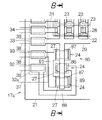
図3は第1実施形態に係る素子ユニット17の平面図を概略的に示す。素子ユニット17は基体21を備える。基体21には素子アレイ22が形成される。素子アレイ22は超音波トランスデューサー素子(以下「素子」という)23の配列で構成される。配列は複数行複数列のマトリクスで形成される。個々の素子23は圧電素子部24を備える。圧電素子部24は上部電極25、下部電極26および圧電体膜27で構成される。個々の素子23ごとに上部電極25および下部電極26の間に圧電体膜27が挟み込まれる。素子ユニット17は1枚の超音波トランスデューサー素子チップとして構成される。
FIG. 3 schematically shows a plan view of the
基体21の表面には複数本の第1導電体28が形成される。第1導電体28は配列の行方向に相互に平行に延びる。1行の素子23ごとに1本の第1導電体28が割り当てられる。1本の第1導電体28は配列の行方向に並ぶ素子23の圧電体膜27に共通に接続される。第1導電体28は個々の素子23ごとに上部電極25を形成する。第1導電体28の両端は1対の引き出し配線29にそれぞれ接続される。引き出し配線29は配列の列方向に相互に平行に延びる。したがって、全ての第1導電体28は同一長さを有する。こうしてマトリクス全体の素子23に共通に上部電極25は接続される。
A plurality of
基体21の表面には複数本の第2導電体31が形成される。第2導電体31は配列の列方向に相互に平行に延びる。1列の素子23ごとに1本の第2導電体31が割り当てられる。1本の第2導電体31は配列の列方向に並ぶ素子23の圧電体膜27に共通に配置される。列ごとに素子23の通電は切り替えられる。こうした通電の切り替えに応じてラインスキャンやセクタースキャンは実現される。1列の素子23は同時に超音波を出力することから、1列の個数すなわち配列の行数は超音波の出力レベルに応じて決定されることができる。行数は例えば10〜15行程度に設定されればよい。図中では省略されて5行が描かれる。配列の列数はスキャンの範囲の広がりに応じて決定されることができる。列数は例えば128列や256列に設定されればよい。図中では省略されて8列が描かれる。その他、配列では千鳥配置が確立されてもよい。千鳥配置では偶数列の素子23群は奇数列の素子23群に対して行ピッチの2分の1でずらされればよい。奇数列および偶数列の一方の素子数は他方の素子数に比べて1つ少なくてもよい。さらにまた、上部電極25および下部電極26の役割は入れ替えられてもよい。すなわち、マトリクス全体の素子23に共通に下部電極が接続される一方で、配列の列ごとに共通に素子23に上部電極が接続されてもよい。
A plurality of
基体21の輪郭は、相互に平行な1対の直線で仕切られて対向する第1辺21aおよび第2辺21bを有する。第1辺21aと素子アレイ22の輪郭との間に1ラインの第1端子アレイ32aが配置される。第2辺21bと素子アレイ22の輪郭との間に1ラインの第2端子アレイ32bが配置される。第1端子アレイ32aは第1辺21aに平行に1ラインを形成することができる。第2端子アレイ32bは第2辺21bに平行に1ラインを形成することができる。第1端子アレイ32aは1対の上部電極端子33および複数の下部電極端子34で構成される。同様に、第2端子アレイ32bは1対の上部電極端子35および複数の下部電極端子36で構成される。1本の引き出し配線29の両端にそれぞれ上部電極端子33、35は接続される。引き出し配線29および上部電極端子33、35は素子アレイ22を二等分する垂直面で面対称に形成されればよい。1本の第2導電体31の両端にそれぞれ下部電極端子34、36は接続される。第2導電体31および下部電極端子34、36は素子アレイ22を二等分する垂直面で面対称に形成されればよい。ここでは、基体21の輪郭は矩形に形成される。基体21の輪郭は正方形であってもよく台形であってもよい。
The outline of the
基体21には第1フレキシブルプリント配線板(以下「第1配線板」という)37が連結される。第1配線板37は第1端子アレイ32aに覆い被さる。第1配線板37の一端には上部電極端子33および下部電極端子34に個別に対応して導電線すなわち第1信号線38が形成される。第1信号線38は上部電極端子33および下部電極端子34に個別に向き合わせられ個別に接合される。同様に、基体21には第2フレキシブルプリント配線板(以下「第2配線板」という)41が覆い被さる。第2配線板41は第2端子アレイ32bに覆い被さる。第2配線板41の一端には上部電極端子35および下部電極端子36に個別に対応して導電線すなわち第2信号線42が形成される。第2信号線42は上部電極端子35および下部電極端子36に個別に向き合わせられ個別に接合される。
A first flexible printed wiring board (hereinafter referred to as “first wiring board”) 37 is connected to the
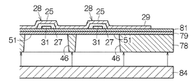
図4に示されるように、基体21は基板44および可撓膜45を備える。基板44の表面に可撓膜45が一面に形成される。基板44には個々の素子23ごとに開口46が形成される。開口46は基板44に対してアレイ状に配置される。開口46が配置される領域の輪郭は素子アレイ22の輪郭に相当する。隣接する2つの開口46の間には仕切り壁(隔壁部)47で区画される。隣接する開口46は仕切り壁47で仕切られる。仕切り壁47の壁厚みは開口46の間隔に相当する。仕切り壁47は相互に平行に広がる平面内に2つの壁面を規定する。壁厚みは2つの壁面の距離に相当する。すなわち、壁厚みは壁面に直交して壁面の間に挟まれる垂線の長さで規定されることができる。
As shown in FIG. 4, the
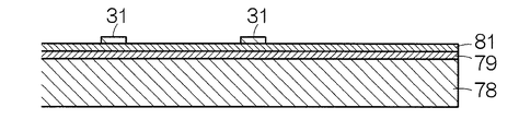
可撓膜45は、基板44の表面に積層される酸化シリコン(SiO2)層48と、酸化シリコン層48の表面に積層される酸化ジルコニウム(ZrO2)層49とで構成される。可撓膜45は開口46に接する。こうして開口46の輪郭に対応して可撓膜45の一部が振動膜51を形成する。振動膜51は、可撓膜45のうち、開口46に臨むことから基板44の厚み方向に膜振動することができる部分である。酸化シリコン層48の膜厚は共振周波数に基づき決定されることができる。
The
振動膜51の表面に第2導電体31、圧電体膜27および第1導電体28が順番に積層される。第2導電体31には例えばチタン(Ti)、イリジウム(Ir)、白金(Pt)およびチタン(Ti)の積層膜が用いられることができる。圧電体膜27は例えばジルコン酸チタン酸鉛(PZT)で形成されることができる。第1導電体28は例えばイリジウム(Ir)で形成されることができる。第1導電体28および第2導電体31にはその他の導電材が利用されてもよく、圧電体膜27にはその他の圧電材料が用いられてもよい。ここでは、第1導電体28の下で圧電体膜27は完全に第2導電体31を覆う。圧電体膜27の働きで第1導電体28と第2導電体31との間で短絡は回避されることができる。
The
基体21の表面には保護膜53が積層される。保護膜53は例えば全面にわたって基体21の表面に覆い被さる。その結果、素子アレイ22や第1および第2端子アレイ32a、32b、第1および第2配線板37、41は保護膜53で覆われる。保護膜53には例えばシリコーン樹脂膜が用いられることができる。保護膜53は、素子アレイ22の構造や、第1端子アレイ32aおよび第1配線板37の接合、第2端子アレイ32bおよび第2配線板41の接合を保護する。
A
基体21の裏面には補強板54が固定される。補強板54の表面に基体21の裏面が重ねられる。補強板54は素子ユニット17の裏面で開口46を閉じる。補強板54はリジッドな基材を備えることができる。補強板54は例えばシリコン基板から形成されることができる。基体21の板厚は例えば100μm程度に設定され、補強板54の板厚は例えば100〜150μm程度に設定される。ここでは、仕切り壁47は補強板54に結合される。補強板54は個々の仕切り壁47に少なくとも1カ所の接合域で接合される。接合にあたって接着剤は用いられることができる。
A reinforcing
(2)超音波診断装置の回路構成
図5に示されるように、超音波診断装置11は素子ユニット17に電気的に接続される集積回路チップ58を備える。集積回路チップ58はマルチプレクサー59および送受信回路61を備える。マルチプレクサー59は素子ユニット17側のポート群59aと送受信回路61側のポート群59bとを備える。素子ユニット17側のポート群59aには配線62経由で第1信号線38および第2信号線42が接続される。こうしてポート群59aは素子アレイ22に繋がる。ここでは、送受信回路61側のポート群59bには集積回路チップ55内の規定数の信号線63が接続される。規定数はスキャンにあたって同時に出力される素子23の列数に相当する。マルチプレクサー59はケーブル14側のポートと素子ユニット17側のポートとの間で相互接続を管理する。
(2) Circuit Configuration of Ultrasonic Diagnostic Device As shown in FIG. 5, the ultrasonic
送受信回路61は規定数の切り替えスイッチ64を備える。個々の切り替えスイッチ64はそれぞれ個別に対応の信号線63に接続される。送受信回路61は個々の切り替えスイッチ64ごとに送信経路65および受信経路66を備える。切り替えスイッチ64には送信経路65と受信経路66とが並列に接続される。切り替えスイッチ64はマルチプレクサー59に選択的に送信経路65または受信経路66を接続する。送信経路65にはパルサー67が組み込まれる。パルサー67は振動膜52の共振周波数に応じた周波数でパルス信号を出力する。受信経路66にはアンプ68、ローパスフィルター(LPF)69およびアナログデジタル変換器(ADC)71が組み込まれる。個々の素子23の出力信号は増幅されてデジタル信号に変換される。
The transmission /
送受信回路61は駆動/受信回路72を備える。送信経路65および受信経路66は駆動/受信回路72に接続される。駆動/受信回路72はスキャンの形態に応じて同時にパルサー67を制御する。駆動/受信回路72はスキャンの形態に応じて出力信号のデジタル信号を受信する。駆動/受信回路72は制御線73でマルチプレクサー59に接続される。マルチプレクサー59は駆動/受信回路72から供給される制御信号に基づき相互接続の管理を実施する。
The transmission /
装置端末12には処理回路74が組み込まれる。処理回路74は例えば中央演算処理装置(CPU)やメモリーを備えることができる。超音波診断装置11の全体動作は処理回路74の処理に従って制御される。ユーザーから入力される指示に応じて処理回路74は駆動/受信回路72を制御する。処理回路74は素子23の出力信号に応じて画像を生成する。画像は描画データで特定される。
A
装置端末12には描画回路75が組み込まれる。描画回路75は処理回路74に接続される。描画回路75にはディスプレイパネル15が接続される。描画回路75は処理回路74で生成された描画データに応じて駆動信号を生成する。駆動信号はディスプレイパネル15に送り込まれる。その結果、ディスプレイパネル15に画像が映し出される。
A
(3)超音波診断装置の動作
次に超音波診断装置11の動作を簡単に説明する。処理回路74は超音波診断モードと感度検出モードとを切り替える。超音波診断モードでは超音波診断装置11で超音波診断が実施されることができる。感度検出モードでは圧電素子部24の感度の低下が判定されることができる。処理回路74が超音波診断モードを選択すると、処理回路74は駆動/受信回路72に超音波の送信および受信を指示する。駆動/受信回路72はマルチプレクサー59に制御信号を供給するとともに個々のパルサー67に駆動信号を供給する。パルサー67は駆動信号の供給に応じてパルス信号を出力する。マルチプレクサー59は制御信号の指示に従ってポート群59bのポートにポート群59aのポートを接続する。パルス信号はポートの選択に応じて上部電極端子33、35および下部電極端子34、36を通じて列ごとに素子23に供給される。パルス信号の供給に応じて振動膜53は振動する。その結果、対象物(例えば人体の内部)に向けて所望の超音波ビームは発せられる。
(3) Operation of Ultrasonic Diagnostic Device Next, the operation of the ultrasonic
超音波の送信後、切り替えスイッチ64は切り替えられる。マルチプレクサー59はポートの接続関係を維持する。切り替えスイッチ64は送信経路65および信号線63の接続に代えて受信経路66および信号線63の接続を確立する。超音波の反射波は振動膜43を振動させる。その結果、素子23から出力信号が出力される。出力信号はデジタル信号に変換されて駆動/受信回路72に送り込まれる。
After transmission of the ultrasonic wave, the
超音波の送信および受信は繰り返される。繰り返しにあたってマルチプレクサー59はポートの接続関係を変更する。その結果、ラインスキャンやセクタースキャンは実現される。スキャンが完了すると、処理回路74は出力信号のデジタル信号に基づき画像を形成する。形成された画像はディスプレイパネル15の画面に表示される。
Transmission and reception of ultrasonic waves are repeated. In the repetition, the
図6に示されるように、処理回路74が感度検出モードを選択すると、処理回路74はステップS1で特定の1列の素子23群(以下「対象検出素子列」という)を選択する。ここでは、図3に示されるように、複数本の第2導電体31のうち、最も外側に位置する2本の第2導電体31以外の1本の第2導電体31に接続される素子23群が対象検出素子列76として選択されることができる。この選択に応じて駆動/受信回路72はマルチプレクサー59に制御信号を供給する。制御信号では、対象検出素子列76と、対象検出素子列76の両側に隣接する2列の素子23群(以下「対象駆動素子列」という)とが特定される。マルチプレクサー59は、制御信号の指示に従って、ポート群59bの任意のポートに、対象検出素子列76および対象駆動素子列77にそれぞれ繋がるポート群59aのポートを個別に接続する。切り替えスイッチ64の切り替えに応じて、対象検出素子列76は受信経路66に接続され、2列の対象駆動素子列77はそれぞれ送信経路65に接続される。
As shown in FIG. 6, when the
処理回路74はステップS2で対象駆動素子列77に対する駆動信号の供給を指示する。処理回路74は2つのパルサー67に駆動信号を供給する。パルサー67は駆動信号の供給に応じてパルス信号(駆動信号)を出力する。パルス信号は第1導電体28および第2導電体31を通じて対象駆動素子列77に供給される。こうして対象駆動素子列77では個々の圧電素子部24に電圧が印加される。このとき、駆動/受信回路72は、一部の素子23の圧電素子部24に駆動信号を入力する入力部として機能する。
The
対象駆動素子列77では駆動信号の供給に応じて圧電体膜27は変形する。圧電体膜27の変形は振動膜51の変形すなわち振動を引き起こす。図7に示されるように、対象駆動素子列77の振動膜51の振動に応じて基板44の仕切り壁47は振動する。仕切り壁47の振動は対象検出素子列76の振動膜51で振動を引き起こす。この振動に応じて対象検出素子列76の圧電体膜27では応力が生成される。応力の生成に応じて圧電体膜27では起電圧が生成される。起電圧は出力信号として出力される。対象検出素子列76は対象駆動素子列77に隣接することから、対象駆動素子列77の振動膜51は確実に対象検出素子列76の振動膜51の変形を引き起こすことができる。
In the target
処理回路74はステップS3で対象検出素子列76に対する出力信号の受信を指示する。出力信号はデジタル信号に変換されて駆動/受信回路72に送り込まれる。このとき、駆動/受信回路72は、圧電素子のうちの一部の圧電素子すなわち対象駆動素子列77の圧電素子部24に駆動信号が入力されている期間に、圧電素子のうちの駆動信号が入力されていない圧電素子すなわち対象検出素子列76の圧電素子部24の振動を検出する検出部として機能する。処理回路74は出力信号の検出値を特定する。特定された検出値はステップS4で予め決められた閾値に比べられる。閾値は例えば処理回路74のメモリといった記憶部に予め格納されていればよい。検出値が閾値以上であれば、感度は良好と判断される。感度検出モードは終了する。検出値が閾値を下回れば、処理回路74は圧電体膜27の分極量の低下を判別する。圧電素子部24の感度の低下すなわち「異常」が判断される。こうして「異常」が検出されると、処理回路74はステップS5で分極処理の実施を指示する。分極処理が実施されると、個々の圧電体膜27に分極用電圧が供給される。圧電体膜27では分極用電圧の印加に応じて分極が実現される。
The
前述のように、素子ユニット17では使用に先立って個々の圧電体膜27で分極が確立される。分極量は時間の経過とともに低下する。その結果、素子23の感度は低下していく。したがって、素子23の感度の低下が検出された際に圧電体膜27に改めて分極用電圧が供給されれば、圧電体膜27では再び十分な分極が確立されることができる。素子23の感度は良好な状態に戻されることができる。
As described above, in the
素子ユニット17では超音波診断にあたって素子アレイ22全体の素子23が超音波の発信および受信を実施する。個々の素子23は超音波の送信と受信とで切り替えられる。素子23は送信時に振動膜51から超音波ビームを放射する。受信時には、対象物から反射してきた超音波は当該振動膜51の振動を引き起こす。こうして反射してきた超音波に応じて素子23から出力信号は出力される。そして、素子アレイ22中の3列の素子23群が感度の判定にあたって利用される。したがって、感度の判定にあたってそれ専用の構造が改めて付加される必要はない。感度の判定は簡単に実現されることができる。
In the
この例では、感度の判定にあたって検出対象である1列の素子23の振動膜51に両側の2列の素子23から変形力が加えられる。したがって、単純に片側の1列の素子23から変形力が加えられる場合に比べて、一度の駆動信号の供給で検出対象である圧電体膜27の応力は増大することができる。圧電体膜27の起電圧は増大する。その結果、判定の精度は高められることができる。素子ユニット17では各列ごとに全列で感度の判定が実施されることもできる。この場合には、素子アレイ22の両端の列では検出対象である圧電体膜27に片側の1列の素子23からのみ変形力が加えられる。その他、素子アレイ22の両端の列は感度の判定にあたってのみ駆動電圧を受信し超音波診断モードでは利用されなくてもよい。
In this example, a deformation force is applied from the two rows of
分極量の低下の判別にあたって、ステップS4の検出値および閾値の比較に代えて、出力信号の信号波形の変化率が観察されてもよい。例えば信号レベルの立ち上がりが閾値以上であれば、感度は良好と判断されることができる。信号レベルの立ち上がりが閾値を下回れば、分極量の低下は判別されることができる。信号レベルの立ち上がりは、所定の時間間隔で検出される信号レベルの大きさに基づき特定されることができる。 In determining the decrease in the polarization amount, the rate of change in the signal waveform of the output signal may be observed instead of comparing the detected value and the threshold value in step S4. For example, if the rise of the signal level is equal to or higher than the threshold value, the sensitivity can be determined to be good. If the rise of the signal level falls below the threshold value, a decrease in the polarization amount can be determined. The rise of the signal level can be specified based on the magnitude of the signal level detected at a predetermined time interval.
その他、ステップS5の分極処理に代えて処理回路74は「異常」の検出に応じて通知信号を生成してもよい。例えば通知信号には感度の低下を表示する画像信号が含まれることができる。こうした画像信号は描画回路75に送り込まれることができる。感度の低下はディスプレイパネル15の画面表示でユーザーに通知されることができる。こうしてユーザーは圧電体膜27の感度低下を知ることができる。こうした通知に応じてプローブヘッド13bや素子ユニット17が交換されてもよく外部装置を通じて圧電体膜27の分極処理が実施されてもよい。
In addition, instead of the polarization process in step S5, the
通知信号には、前述の画像信号に代えて、起電圧の大きさを示す画像信号が含まれてもよい。起電圧の大きさはディスプレイパネル15の画面表示でユーザーに提示されることができる。ユーザーは起電圧の大きさに基づき分極量が適正か否かを判断することができる。こうした通知信号の出力にあたって、処理回路74は、対象駆動素子列77の圧電素子部24に駆動信号を入力する駆動期間の積分信号を出力することができる。こうして駆動期間分の出力信号の積分値が取得されることができる。
The notification signal may include an image signal indicating the magnitude of the electromotive voltage instead of the above-described image signal. The magnitude of the electromotive voltage can be presented to the user on the screen display of the
(4)超音波トランスデューサー素子ユニットの製造方法
図8に示されるように、シリコンウエハー78の表面で個々の素子ユニット17ごとに第2導電体31および下部電極端子34、36(図8以降では図示されず)を形成する。第2導電体31および下部電極端子34、36の形成に先立ってシリコンウエハー78の表面に酸化シリコン膜79および酸化ジルコニウム膜81を相次いで形成する。酸化ジルコニウム膜81の表面に導電膜を形成する。導電膜はチタン、イリジウム、白金およびチタンの積層膜で構成される。フォトリソグラフィ技術に基づき導電膜から第2導電体31および下部電極端子34、36を成形する。
(4) Manufacturing Method of Ultrasonic Transducer Element Unit As shown in FIG. 8, the
図9に示されるように、第2導電体31の表面で個々の素子23ごとに圧電体膜27および第1導電膜82を形成する。圧電体膜27および第1導電膜82の形成にあたってシリコンウエハー78の表面に圧電材料膜および導電材の膜を成膜する。圧電材料膜はPZT膜から構成される。導電材の膜はイリジウム膜から構成される。フォトリソグラフィ技術に基づき個々の素子23ごとに圧電材料膜および導電材の膜から圧電体膜27および第1導電膜82を成形する。
As shown in FIG. 9, the
続いて、図10に示されるように、シリコンウエハー78の表面に導電材の膜83を成膜する。導電材の膜83は個々の第1導電膜82に覆い被さる。隣接する第1導電膜82は膜83で相互に接続される。そして、フォトリソグラフィ技術に基づき膜83から第2導電膜を成形する。第2導電膜は、第1導電体31に直交する方向に延び、次々と第1導電体31を横切る。第2導電膜は素子アレイ22の行方向に第1導電膜82を相互に接続する。第2導電膜は第2導電体31、引き出し配線29および上部電極端子33、35を形成する。第2導電膜の一部は第1導電膜82に重なって第1導電膜82とともに上部電極25を形成する。
Subsequently, as shown in FIG. 10, a
その後、図11に示されるように、シリコンウエハー78の裏面からアレイ状の開口46を形成する。開口46の形成にあたってエッチング処理を施す。酸化シリコン膜79はエッチングストップ層として機能する。酸化シリコン膜79および酸化ジルコニウム膜81に振動膜51は区画される。開口46の形成後、シリコンウエハー78の裏面に補強板用のウエハー84の表面を重ね合わせる。重ね合わせに先立ってウエハー84はハンドリング機構やステージ上に保持される。ウエハー84には例えばリジッドな絶縁性基板が用いられることができる。絶縁性基板にはシリコンウエハーが用いられることができる。接合にあたって例えば接着剤が用いられることができる。接合後、シリコンウエハー78から個々の素子ユニット17を切り出す。切り出した素子ユニット17で分極処理を実施する。個々の圧電体膜27に分極用電圧が印加される。
Thereafter, as shown in FIG. 11, an array-shaped
(5)第2実施形態に係る超音波トランスデューサー素子ユニット
図12は第2実施形態に係る素子ユニット17aの構造を概略的に示す。第2実施形態では基体21上に前述の素子アレイ22に加えて感度検出モードに専用の圧電素子セット85が形成される。素子アレイ22は前述のように第1素子23の配列で構成される。圧電素子セット85は素子アレイ22の輪郭の外側に配置される。圧電素子セット85は1つの第2素子86および1対の第3素子87を備える。第2素子86は検出専用の素子として機能する。第3素子87は駆動専用の素子として機能する。第2素子86は2つの第3素子87の間に配置される。第2素子86および第3素子87は第1素子23と同様に圧電素子部24を備える。圧電素子部24は上部電極25、圧電体膜27および下部電極26で構成される。第2素子86は第1素子23と同一構造に形成される。
(5) Ultrasonic Transducer Element Unit According to Second Embodiment FIG. 12 schematically shows the structure of an
基体21の表面には第1補助導電体88が形成される。第1補助導電体88は第2素子86および第3素子87に共通に割り当てられる。第1補助導電体88は第2素子86および第3素子87の圧電体膜27に共通に接続される。第1補助導電体88は個々の素子86、87ごとに上部電極25を形成する。第1補助導電体88の一端は例えば引き出し配線29に接続される。第1補助導電体88は第1導電体28および引き出し配線29と同一の材料から形成されることができる。
A first
基体21の表面には第2補助導電体89が形成される。第2補助導電体89は第2素子86の圧電体膜27に接続される。第2補助導電体89は第2素子86の下部電極26を形成する。こうして第2素子86では圧電体膜27に第1補助導電体88および第2補助導電体89から駆動電圧が印加される。第2補助導電体89は第2導電体31と同一の材料から形成されることができる。
A second
基体21の表面には第3補助導電体91が形成される。第3補助導電体91は第3素子87の圧電体膜27に共通に接続される。第3補助導電体91は第3素子87の下部電極26を形成する。こうして第3素子87では圧電体膜27に第1補助導電体88および第3補助導電体91から駆動電圧が印加される。第3補助導電体91は第2導電体31と同一の材料から形成されることができる。
A third
第1端子アレイ32aには第1補助電極端子92および第2補助電極端子93が組み込まれる。第1補助電極端子92は第2補助導電体89に電気的に接続される。第1補助電極端子92は第2補助導電体89に一体化されることができる。第2補助電極端子93は第3補助導電体91に電気的に接続される。第2補助電極端子93は第3補助導電体91に一体化されることができる。第1補助電極端子92および第2補助電極端子93は第1配線板37の第1信号線38に個別に接合される。
A first
図13に示されるように、基板44には前述の第1開口46に加えて第2開口94および第3開口95が形成される。第2開口94は第2素子86の振動膜51を区画する。第3開口95は第3素子87の振動膜51を区画する。したがって、第2開口94および第3開口95は素子アレイ22の輪郭の外側に配置される。第3開口95は第1開口46よりも第2開口94に近接して配置される。第2開口94上に第2素子86の圧電素子部24は配置される。第3開口95上に第3素子87の圧電素子部24は配置される。こうして第2素子86および第3素子87の圧電素子部24は個々に対応する振動膜51に結合される。
As shown in FIG. 13, a
このとき、第3素子87の圧電素子部24は第1および第2素子23、86の圧電素子部24よりも大きい面積で形成される。具体的には、第2素子86の輪郭の中心軸に直交する方向に第3素子87の圧電素子部24は第2素子86の圧電素子部24の第1幅W1よりも大きい第2幅W2を有する。しかも、第3素子87の圧電素子部24は第3開口95の輪郭の外側まで広がる。すなわち、第3素子87の圧電素子部24は第3開口95を横切って基板44の対岸を接続する。圧電素子部24の大きさは圧電体膜27のうち上部電極25および下部電極26で挟まれる領域で規定されればよい。
At this time, the
図14に示されるように、第2実施形態に係る素子ユニット17aの利用にあたって超音波診断装置11の集積回路チップ58では前述の上部電極端子33、35および下部電極端子34、36に加えて配線62経由で第1補助電極端子92および第2補助電極端子93がマルチプレクサー59のポート群59aに接続される。処理回路74で感度検出モードが選択されると、マルチプレクサー59の働きで第1補助電極端子92は受信経路66に接続され第2補助電極端子93は送信経路に接続される。その他の構成および動作は前述と同様である。
As shown in FIG. 14, in using the
処理回路74が超音波診断モードを選択すると、前述と同様に、上部電極端子33、35および下部電極端子34、36を通じて素子アレイ22内の第1素子23に駆動信号は供給される。マルチプレクサー59の働きでラインスキャンやセクタースキャンは実現される。検出信号に応じてディスプレイパネル15の画面に画像が表示される。
When the
処理回路74が感度検出モードを選択すると、駆動/受信回路72はマルチプレクサー59に制御信号を供給する。制御信号では第2素子86および第3素子87が特定される。マルチプレクサー59は、制御信号の指示に従って、ポート群59bの任意のポートに、第1補助電極端子92および第2補助電極端子93に繋がるポート群59aのポートを個別に接続する。切り替えスイッチ64の切り替えに応じて、第1補助電極端子92は受信経路66に接続され、第2補助電極端子93は送信経路65に接続される。
When the
処理回路74は第3素子87に対する駆動信号の供給を指示する。処理回路74はパルサー67に駆動信号を供給する。パルサー67は駆動信号の供給に応じてパルス信号(駆動信号)を出力する。パルス信号は第1補助導電体88および第2補助導電体89を通じて第3素子87に供給される。
The
第3素子87では駆動信号の供給に応じて圧電体膜27は変形する。圧電体膜27の変形は振動膜51の変形を引き起こす。第3素子87の振動膜51の変形は第2素子86の振動膜51で変形を引き起こす。この変形に応じて第2素子86の圧電体膜27では応力が生成される。応力の生成に応じて圧電体膜27では起電圧が生成される。起電圧は出力信号として出力される。
In the
処理回路74は第2素子86に対する出力信号の受信を指示する。出力信号はデジタル信号に変換されて駆動/受信回路72に送り込まれる。処理回路74は出力信号の検出値を特定する。特定された検出値は予め決められた閾値に比べられる。検出値が閾値以上であれば、感度検出モードは終了する。検出値が閾値を下回れば、処理回路74は圧電体膜27の分極量の低下を認定する。一般に、第2素子86の特性は第1圧電素子23の特性を反映することから、第2素子86の異常に基づき第1素子23の異常は推定されることができる。こうして第2素子86で圧電素子部24の感度の低下すなわち「異常」が判断されると、前述と同様に、処理回路74は分極処理の実施を指示してもよく通知信号を生成してもよい。
The
ここでは、第2素子86は第1素子23と同一の構造を有する。第2開口94は第1開口46と同一の形状に形成される。振動膜51は同一形状および同一膜厚を有する。圧電素子部24は同一の構造を有する。こうして第2素子86の特性は第1素子23の特性に簡単に関連づけられることができる。第2素子86の特性は第1素子23の特性を高い精度で反映することができる。素子アレイ22内では個々の素子で特性のばらつきは小さいことから、1つの第2素子86で特性が特定されれば、全ての第1素子23の特性は推定されることができる。
Here, the
圧電素子セット85では検出対象である第2素子86の振動膜51に両側の第3素子87から変形力が加えられる。したがって、単純に片側から変形力が加えられる場合に比べて、一度の駆動信号の供給で検出対象である圧電体膜27の応力は増大することができる。圧電体膜27の起電圧は増大する。その結果、判定の精度は高められることができる。しかも、第3素子87では振動膜51は圧電体膜27の変形を増幅することができる。その結果、第2素子86の圧電体膜27の変形は増大することができる。判定の精度は一層高められることができる。ただし、第3素子87の圧電体から第2素子86の圧電体膜27に十分な変形力が加わる限り、第3素子87では振動膜51は省略されることができる。
In the piezoelectric element set 85, a deformation force is applied from the
圧電素子セット85では第3素子87の圧電素子部24は第2素子86の圧電素子部24よりも大きく形成される。こうして第2素子86にはより大きい変形力が加えられることができる。その結果、判定の精度は高められることができる。圧電素子セット85は素子アレイ22の輪郭の外側に配置されることから、第3素子87の拡大は素子アレイ22内の第1素子23には影響しない。
In the piezoelectric element set 85, the
加えて、第3素子87の圧電素子部24は第3開口95の輪郭の外側まで広がる。第3素子87の変形は直接的に第2開口94の周囲の基板44すなわち仕切り壁47に伝達されることができる。したがって、第3素子87の変形が振動膜51を通じて第2開口94の周囲の基板44に伝達される場合に比べて、第3素子87の変形は効率的に第2素子86に伝達されることができる。その結果、第2素子86の応力は増大することができる。判定の精度は高められることができる。
In addition, the
(6)第3実施形態に係る超音波トランスデューサー素子ユニット
図15は第3実施形態に係る素子ユニット17bの構造を概略的に示す。第3実施形態では基体21上に前述の圧電素子セット85に代えて感度検出モードに専用の単一の第2素子86が基体21上に形成される。第2素子86は素子アレイ22の輪郭の外側に配置される。第2素子86は第1素子23と同様に圧電素子部24を備える。第2素子86は第1素子23と同一構造に形成される。第2補助導電体89は第2素子86の圧電体膜27に接続される。第1補助電極端子92は第2補助導電体89に電気的に接続される。その他の構成および動作は前述と同様である。
(6) Ultrasonic Transducer Element Unit According to Third Embodiment FIG. 15 schematically shows the structure of an
処理回路74が感度検出モードを選択すると、駆動/受信回路72はマルチプレクサー59に制御信号を供給する。制御信号では第2素子86および第2素子86に最も近い1列の第1素子23群(以下「対象駆動素子列」という)が特定される。マルチプレクサー59は、制御信号の指示に従って、ポート群59bの任意のポートに、対象駆動素子列および第2補助電極端子93に繋がるポート群59aのポートを個別に接続する。切り替えスイッチ64の切り替えに応じて、第1補助電極端子92は受信経路66に接続され、第2補助電極端子93は送信経路65に接続される。
When the
(7)他の実施形態に係る超音波診断装置
図16は他の実施形態に係る超音波診断装置11aの回路構成を概略的に示す。超音波診断装置11aでは素子ユニット17、17a、17bに集積回路チップ58aが接続される。素子ユニット17、17a、17bでは素子アレイ22の列ごとに送信用の素子23と受信用の素子23とが割り当てられる。送信用の列と受信用の列とは例えば交互に配置されることができる。集積回路チップ58aでは送信経路65および受信経路66が個別にマルチプレクサー59に接続される。マルチプレクサー59は超音波の送信時には送信用の列ごとに素子23に送信経路65を接続する。マルチプレクサー59は超音波の受信時には受信用の列ごとに素子23に受信経路66を接続する。送信経路65に接続される素子23は超音波の送信を担当する。受信経路66に接続される素子23は超音波の受信を担当する。こうして個々の素子23ごとに超音波の送信および受信が分担されることから、個々の素子23は超音波の送信または受信に特化して調整されることができる。その結果、超音波の受信感度は向上することができる。
(7) Ultrasonic Diagnostic Apparatus According to Other Embodiment FIG. 16 schematically shows a circuit configuration of an ultrasonic
なお、上記のように本実施形態について詳細に説明したが、本発明の新規事項および効果から実体的に逸脱しない多くの変形が可能であることは当業者には容易に理解できるであろう。したがって、このような変形例はすべて本発明の範囲に含まれる。例えば、明細書または図面において、少なくとも一度、より広義または同義な異なる用語とともに記載された用語は、明細書または図面のいかなる箇所においても、その異なる用語に置き換えられることができる。また、超音波診断装置11、11a、超音波プローブ13、プローブヘッド13b、素子ユニット17、17a、素子23、86、87、集積回路チップ58、58a等の構成および動作も本実施形態で説明したものに限定されず、種々の変形が可能である。
Although the present embodiment has been described in detail as described above, it will be easily understood by those skilled in the art that many modifications can be made without departing from the novel matters and effects of the present invention. Therefore, all such modifications are included in the scope of the present invention. For example, a term described with a different term having a broader meaning or the same meaning at least once in the specification or the drawings can be replaced with the different term in any part of the specification or the drawings. The configuration and operation of the ultrasonic
11 電子機器としての超音波診断装置、11a 電子機器としての超音波診断装置、13 プローブ(超音波プローブ)、13b プローブヘッド、15 表示装置(ディスプレイパネル)、16 筐体、17 超音波トランスデューサー装置の一部を構成する超音波トランスデューサー素子ユニット、17a 超音波トランスデューサー装置の一部を構成する超音波トランスデューサー素子ユニット、17b 超音波トランスデューサー装置の一部を構成する超音波トランスデューサー素子ユニット、23 (第1)超音波トランスデューサー素子、24 (第1および第2)圧電素子(圧電素子部)、44 基板、46 (第1)開口、51 振動膜、64 切り替えスイッチ、65 送信経路、66 受信経路、72 入力部および検出部(駆動/受信回路)、74 処理部としての処理回路、94 第2開口、95 第3開口。
DESCRIPTION OF
Claims (15)
前記基板に設けられた振動膜と、
前記振動膜上であって、前記基板の厚み方向の平面視において前記第1開口に重なる位置に設けられた第1圧電素子と、
前記振動膜上であって、前記基板の厚み方向の平面視において前記第2開口に重なる位置に設けられた第2圧電素子と、
前記第1圧電素子に駆動信号を入力する入力部と、
前記第1圧電素子に前記駆動信号が入力されている期間に、前記駆動信号が入力されていない前記第2圧電素子の振動を検出する検出部と、
前記駆動信号が入力されていない前記第2圧電素子の振動を検出した検出結果に基づき前記第1圧電素子の感度を判別する制御処理部と、を備える、
ことを特徴とする超音波トランスデューサー装置。 A substrate having a first opening and a second opening ;
A vibration film provided on the substrate;
A first piezoelectric element provided on the vibration film at a position overlapping the first opening in a plan view in the thickness direction of the substrate;
A second piezoelectric element provided on the vibration film and in a position overlapping the second opening in a plan view in the thickness direction of the substrate;
An input unit for inputting a drive signal to the first piezoelectric element;
A detection unit that detects vibration of the second piezoelectric element in which the drive signal is not input during a period in which the drive signal is input to the first piezoelectric element;
A control processing unit for determining sensitivity of the first piezoelectric element based on a detection result of detecting vibration of the second piezoelectric element to which the drive signal is not input .
An ultrasonic transducer device.
前記第1圧電素子と前記第2圧電素子とが隣接している、ことを特徴とする超音波トランスデューサー装置。 The ultrasonic transducer device according to claim 1 ,
The ultrasonic transducer device, wherein the first piezoelectric element and the second piezoelectric element are adjacent to each other.
前記基板に設けられた第3開口と、
前記基板の厚み方向の平面視において前記第3開口に重なる位置に設けられ、かつ、前記第2圧電素子に隣接し、前記第1圧電素子とは反対側に設けられた第3圧電素子と、を備え、
前記検出部は、前記第1圧電素子および前記第3圧電素子に前記駆動信号が入力されている期間に、前記第2圧電素子の振動を検出する、
ことを特徴とする超音波トランスデューサー装置。 The ultrasonic transducer device according to claim 2 ,
A third opening provided in the substrate;
A third piezoelectric element provided at a position overlapping the third opening in a plan view in the thickness direction of the substrate , adjacent to the second piezoelectric element, and provided on the opposite side of the first piezoelectric element ; With
The detection unit detects vibration of the second piezoelectric element during a period in which the drive signal is input to the first piezoelectric element and the third piezoelectric element.
An ultrasonic transducer device.
前記制御処理部は、前記駆動信号を入力しない前記第2圧電素子の感度が所定値以下と判別されると、前記駆動信号を入力しない前記第2圧電素子に分極用電圧を供給する、
ことを特徴とする超音波トランスデューサー装置。 The ultrasonic transducer device according to any one of claims 1 to 3 ,
The control processing unit supplies a polarization voltage to the second piezoelectric element that does not input the driving signal when it is determined that the sensitivity of the second piezoelectric element that does not input the driving signal is equal to or less than a predetermined value.
An ultrasonic transducer device.
前記制御処理部は、前記駆動信号を入力しない前記第2圧電素子の感度が所定値以下と判別されると、感度が前記所定値以下を示す通知信号を出力する、
ことを特徴とする超音波トランスデューサー装置。 The ultrasonic transducer device according to any one of claims 1 to 3 ,
The control processing unit outputs a notification signal indicating that the sensitivity is equal to or lower than the predetermined value when it is determined that the sensitivity of the second piezoelectric element that does not receive the drive signal is equal to or lower than the predetermined value.
An ultrasonic transducer device.
前記基板は、前記第1開口と前記第2開口とに挟まれた部分である隔壁部を有し、
前記隔壁部は、前記基板の厚み方向の平面視における前記第1開口と前記第2開口との間の距離の最小値より前記基板の厚み方向の厚みが大きい形状を有する、
ことを特徴とする超音波トランスデューサー装置。 In the ultrasonic transducer device according to any one of claims 1 to 5 ,
The substrate has a partition wall portion that is a portion sandwiched between the first opening and the second opening;
The partition wall has a shape in which the thickness in the thickness direction of the substrate is larger than the minimum value of the distance between the first opening and the second opening in a plan view in the thickness direction of the substrate.
An ultrasonic transducer device.
前記基板に設けられた振動膜と、
前記振動膜上であって、前記基板の厚み方向の平面視において前記第1開口に重なる位置に設けられ、感度検出モード時に選択される第1圧電素子と、
前記振動膜上であって、前記基板の厚み方向の平面視において前記第2開口に重なる位置に設けられ、前記感度検出モード時に選択される第2圧電素子と、
前記振動膜上であって、前記基板の厚み方向の平面視において前記複数の開口に重なる位置に設けられ、超音波診断モード時に選択される圧電素子群と、
前記第1圧電素子に駆動信号を入力する入力部と、
前記第1圧電素子に前記駆動信号が入力されている期間に、前記駆動信号が入力されていない前記第2圧電素子の振動を検出する検出部と、を備える、
ことを特徴とする超音波トランスデューサー装置。 A first opening, a second opening, and a plurality of openings arranged in a matrix or a line , wherein the first opening and the second opening are contours of a region where the plurality of openings are arranged A substrate disposed on the outside of
A vibration film provided on the substrate;
A first piezoelectric element which is provided on the vibration film and is provided at a position overlapping the first opening in a plan view in the thickness direction of the substrate, and is selected in a sensitivity detection mode;
A second piezoelectric element which is provided on the vibration film and is provided at a position overlapping the second opening in a plan view in the thickness direction of the substrate, and is selected in the sensitivity detection mode;
A piezoelectric element group provided on the vibration film, at a position overlapping the plurality of openings in a plan view in the thickness direction of the substrate, and selected in an ultrasonic diagnostic mode;
An input unit for inputting a drive signal to the first piezoelectric element;
A detection unit that detects vibration of the second piezoelectric element in which the drive signal is not input during a period in which the drive signal is input to the first piezoelectric element.
An ultrasonic transducer device.
前記基板に設けられた第3開口と、 A third opening provided in the substrate;
前記基板の厚み方向の平面視において前記第3開口に重なる位置に設けられ、かつ、前記第2圧電素子に隣接し、前記第1圧電素子とは反対側に設けられた第3圧電素子と、を備え、 A third piezoelectric element provided at a position overlapping the third opening in a plan view in the thickness direction of the substrate, adjacent to the second piezoelectric element, and provided on the opposite side of the first piezoelectric element; With
前記検出部は、前記第1圧電素子および前記第3圧電素子に前記駆動信号が入力されている期間に、前記第2圧電素子の振動を検出する、 The detection unit detects vibration of the second piezoelectric element during a period in which the drive signal is input to the first piezoelectric element and the third piezoelectric element.
ことを特徴とする超音波トランスデューサー装置。An ultrasonic transducer device.
前記第1開口および前記第2開口は同一の形状に形成され、前記第1圧電素子および前記第2圧電素子は同一の構造に形成されている、
ことを特徴とする超音波トランスデューサー装置。 In the ultrasonic transducer device according to any one of claims 1 to 8,
The first opening and the second opening are formed in the same shape, and the first piezoelectric element and the second piezoelectric element are formed in the same structure,
An ultrasonic transducer device.
前記基板の厚み方向の平面視で前記第3圧電素子は前記第2圧電素子よりも大きい面積を有する、
ことを特徴とする超音波トランスデューサー装置。 The ultrasonic transducer device according to claim 3 or 8 ,
The third piezoelectric element has a larger area than the second piezoelectric element in plan view in the thickness direction of the substrate;
An ultrasonic transducer device.
ことを特徴とするプローブ。 The ultrasonic transducer device according to any one of claims 1 to 10, and a housing that supports the ultrasonic transducer device.
A probe characterized by that.
ことを特徴とする電子機器。 The ultrasonic transducer device according to claim 1, and a processing unit that is connected to the ultrasonic transducer device and processes an output of the ultrasonic transducer device.
An electronic device characterized by that.
ことを特徴とする超音波診断装置。 An ultrasonic transducer device according to any one of claims 1 to 10, a processing unit connected to the ultrasonic transducer device, processing an output of the ultrasonic transducer device, and generating an image; A display device for displaying the image,
An ultrasonic diagnostic apparatus.
前記超音波トランスデューサー装置を支持する筐体と、を備える、
ことを特徴とするプローブヘッド。 The ultrasonic transducer device according to any one of claims 1 to 10,
A housing that supports the ultrasonic transducer device,
A probe head characterized by that.
前記開口を塞ぐ振動膜と、
前記振動膜上であって前記開口ごとに設けられる圧電素子と、
複数の前記圧電素子うちの一部の圧電素子に駆動信号を入力する入力部と、
前記一部の圧電素子に前記駆動信号が入力されている期間に、前記駆動信号が入力されていない前記他の一部の圧電素子の振動を検出する検出部と、
前記他の一部の圧電素子の振動を検出した検出結果に基づき前記一部の圧電素子の感度を判別する制御処理部と、を備え、
前記駆動信号が前記一部の圧電素子に入力されることで振動する前記振動膜の振動が前記隔壁部を変形させて前記駆動信号が入力されていない前記他の一部の圧電素子を振動させる、ことを特徴とする超音波トランスデューサー装置。 A substrate having a plurality of openings partitioned by a partition;
A vibrating membrane that closes the opening;
A piezoelectric element provided on each of the openings on the vibrating membrane;
An input unit for inputting a drive signal to a part of the plurality of piezoelectric elements;
A detection unit that detects vibrations of the other part of the piezoelectric elements in which the driving signal is not input during a period in which the driving signal is input to the part of the piezoelectric elements;
A control processing unit for determining sensitivity of the part of the piezoelectric elements based on a detection result of detecting vibration of the other part of the piezoelectric elements ,
The vibration of the vibrating membrane that vibrates when the drive signal is input to the part of the piezoelectric elements deforms the partition and vibrates the other part of the piezoelectric elements to which the drive signal is not input. An ultrasonic transducer device characterized by that.
Priority Applications (3)
| Application Number | Priority Date | Filing Date | Title |
|---|---|---|---|
| JP2012187465A JP6089499B2 (en) | 2012-08-28 | 2012-08-28 | Ultrasonic transducer device and probe, electronic device and ultrasonic diagnostic device |
| CN201310379245.5A CN103654848B (en) | 2012-08-28 | 2013-08-27 | Ultrasound transducer apparatus, detector, electronic equipment and diagnostic ultrasound equipment |
| US14/010,755 US20140066778A1 (en) | 2012-08-28 | 2013-08-27 | Ultrasonic transducer device, probe, electronic instrument, and ultrasonic diagnostic device |
Applications Claiming Priority (1)
| Application Number | Priority Date | Filing Date | Title |
|---|---|---|---|
| JP2012187465A JP6089499B2 (en) | 2012-08-28 | 2012-08-28 | Ultrasonic transducer device and probe, electronic device and ultrasonic diagnostic device |
Publications (3)
| Publication Number | Publication Date |
|---|---|
| JP2014042714A JP2014042714A (en) | 2014-03-13 |
| JP2014042714A5 JP2014042714A5 (en) | 2015-10-08 |
| JP6089499B2 true JP6089499B2 (en) | 2017-03-08 |
Family
ID=50188446
Family Applications (1)
| Application Number | Title | Priority Date | Filing Date |
|---|---|---|---|
| JP2012187465A Active JP6089499B2 (en) | 2012-08-28 | 2012-08-28 | Ultrasonic transducer device and probe, electronic device and ultrasonic diagnostic device |
Country Status (3)
| Country | Link |
|---|---|
| US (1) | US20140066778A1 (en) |
| JP (1) | JP6089499B2 (en) |
| CN (1) | CN103654848B (en) |
Families Citing this family (21)
| Publication number | Priority date | Publication date | Assignee | Title |
|---|---|---|---|---|
| JP5678670B2 (en) * | 2011-01-06 | 2015-03-04 | セイコーエプソン株式会社 | Ultrasonic sensor, tactile sensor, and gripping device |
| JP5990929B2 (en) * | 2012-02-24 | 2016-09-14 | セイコーエプソン株式会社 | Ultrasonic transducer device and probe, electronic device and ultrasonic diagnostic device |
| JP6234788B2 (en) * | 2013-11-19 | 2017-11-22 | 東芝メディカルシステムズ株式会社 | Ultrasonic diagnostic apparatus and program for ultrasonic diagnostic apparatus |
| USD733321S1 (en) * | 2014-01-10 | 2015-06-30 | Celleration, Inc. | Ultrasonic treatment device |
| USD733319S1 (en) * | 2014-01-10 | 2015-06-30 | Celleration, Inc. | Ultrasonic treatment wand |
| JP6519212B2 (en) * | 2014-03-27 | 2019-05-29 | セイコーエプソン株式会社 | Piezoelectric element, piezoelectric device and probe, electronic device and ultrasonic imaging apparatus |
| JP6405737B2 (en) * | 2014-06-18 | 2018-10-17 | コニカミノルタ株式会社 | Acoustic sensor and ultrasonic probe |
| EP3169083A4 (en) * | 2014-07-09 | 2018-05-16 | Seiko Epson Corporation | Ultrasonic sensor and method for manufacturing same |
| JP6476633B2 (en) * | 2014-07-31 | 2019-03-06 | セイコーエプソン株式会社 | Piezoelectric device |
| JP2016033970A (en) * | 2014-07-31 | 2016-03-10 | セイコーエプソン株式会社 | Ultrasonic device and method for manufacturing the same, and probe and electronic equipment |
| JP6314777B2 (en) * | 2014-09-30 | 2018-04-25 | セイコーエプソン株式会社 | Ultrasonic sensor and probe and electronic equipment |
| JP2016086956A (en) * | 2014-10-31 | 2016-05-23 | セイコーエプソン株式会社 | Ultrasonic probe, electronic apparatus, and ultrasonogram device |
| JP6610058B2 (en) * | 2015-07-29 | 2019-11-27 | セイコーエプソン株式会社 | Ultrasonic device and electronic equipment |
| JP6617488B2 (en) * | 2015-09-09 | 2019-12-11 | セイコーエプソン株式会社 | Ultrasonic module, ultrasonic device, and control method of ultrasonic module |
| JP6724502B2 (en) * | 2016-04-06 | 2020-07-15 | セイコーエプソン株式会社 | Ultrasonic device |
| JP6805630B2 (en) | 2016-08-24 | 2020-12-23 | セイコーエプソン株式会社 | Ultrasonic devices, ultrasonic modules, and ultrasonic measuring devices |
| GB2555835B (en) * | 2016-11-11 | 2018-11-28 | Novosound Ltd | Ultrasound transducer |
| JP2018157125A (en) * | 2017-03-21 | 2018-10-04 | セイコーエプソン株式会社 | Piezoelectric element, ultrasonic sensor, discharge head, ultrasonic device, liquid discharge device and manufacturing method of piezoelectric element |
| JP6899804B2 (en) | 2018-06-29 | 2021-07-07 | 富士フイルム株式会社 | How to operate the ultrasonic diagnostic equipment and the ultrasonic diagnostic equipment |
| CN109805958B (en) | 2019-02-22 | 2021-03-16 | 无锡海斯凯尔医学技术有限公司 | Ultrasonic imaging apparatus |
| JP7424069B2 (en) * | 2020-01-21 | 2024-01-30 | セイコーエプソン株式会社 | Ultrasonic devices and sensors |
Family Cites Families (13)
| Publication number | Priority date | Publication date | Assignee | Title |
|---|---|---|---|---|
| JP4723732B2 (en) * | 2000-07-12 | 2011-07-13 | セイコーインスツル株式会社 | Pulse detection device and ultrasonic diagnostic device |
| JP3908512B2 (en) * | 2001-11-16 | 2007-04-25 | セイコーインスツル株式会社 | Piezoelectric transducer and pulse wave detector |
| US6548937B1 (en) * | 2002-05-01 | 2003-04-15 | Koninklijke Philips Electronics N.V. | Array of membrane ultrasound transducers |
| JP4967663B2 (en) * | 2007-01-09 | 2012-07-04 | ソニー株式会社 | Vibration type gyro sensor, control circuit and electronic device |
| JP5274806B2 (en) * | 2007-09-26 | 2013-08-28 | 株式会社東芝 | Ultrasonic diagnostic apparatus and method, and control program for ultrasonic diagnostic apparatus |
| JP2009178262A (en) * | 2008-01-29 | 2009-08-13 | Toshiba Corp | Ultrasonic diagnostic apparatus |
| WO2009126378A2 (en) * | 2008-03-11 | 2009-10-15 | Drexel University | Enhanced detection sensitivity with piezoelectric microcantilever sensors |
| JP5275698B2 (en) * | 2008-06-17 | 2013-08-28 | 富士フイルム株式会社 | Method for polarizing piezoelectric film and method for manufacturing piezoelectric element structure |
| CN101645484B (en) * | 2009-03-02 | 2011-01-05 | 中国科学院声学研究所 | Soft support bridge type silicon micro-piezoelectric ultrasonic transducer chip and prepration method thereof |
| CN101712028B (en) * | 2009-11-13 | 2012-02-01 | 中国科学院声学研究所 | Thin-film ultrasonic transducer and preparation method thereof |
| JP5671876B2 (en) * | 2009-11-16 | 2015-02-18 | セイコーエプソン株式会社 | Ultrasonic transducer, ultrasonic sensor, method for manufacturing ultrasonic transducer, and method for manufacturing ultrasonic sensor |
| JP5401330B2 (en) * | 2010-01-05 | 2014-01-29 | 株式会社日立製作所 | Ultrasonic flaw detection apparatus and ultrasonic flaw detection method |
| JP5505251B2 (en) * | 2010-10-19 | 2014-05-28 | セイコーエプソン株式会社 | Blood vessel diameter measuring device |
-
2012
- 2012-08-28 JP JP2012187465A patent/JP6089499B2/en active Active
-
2013
- 2013-08-27 CN CN201310379245.5A patent/CN103654848B/en active Active
- 2013-08-27 US US14/010,755 patent/US20140066778A1/en not_active Abandoned
Also Published As
| Publication number | Publication date |
|---|---|
| CN103654848B (en) | 2017-07-21 |
| JP2014042714A (en) | 2014-03-13 |
| CN103654848A (en) | 2014-03-26 |
| US20140066778A1 (en) | 2014-03-06 |
Similar Documents
| Publication | Publication Date | Title |
|---|---|---|
| JP6089499B2 (en) | Ultrasonic transducer device and probe, electronic device and ultrasonic diagnostic device | |
| JP5990930B2 (en) | Ultrasonic transducer element chip and probe, electronic device and ultrasonic diagnostic apparatus | |
| JP6078994B2 (en) | Ultrasonic transducer element unit, probe, probe head, electronic device, and ultrasonic diagnostic apparatus | |
| JP5990929B2 (en) | Ultrasonic transducer device and probe, electronic device and ultrasonic diagnostic device | |
| JP6102075B2 (en) | Ultrasonic transducer element chip and probe, electronic device and ultrasonic diagnostic apparatus | |
| JP6136464B2 (en) | ULTRASONIC TRANSDUCER DEVICE AND PROBE, ELECTRONIC DEVICE, AND ULTRASONIC IMAGING DEVICE | |
| JP6102284B2 (en) | Ultrasonic measuring device, ultrasonic head unit, ultrasonic probe, and ultrasonic imaging device | |
| JP5900107B2 (en) | Ultrasonic transducer element chip and probe, electronic device and ultrasonic diagnostic apparatus | |
| JP5978649B2 (en) | Ultrasonic transducer element chip, probe head and probe, electronic device and ultrasonic diagnostic apparatus | |
| JP6252279B2 (en) | ULTRASONIC TRANSDUCER DEVICE AND PROBE, ELECTRONIC DEVICE, AND ULTRASONIC IMAGING DEVICE | |
| JP6273743B2 (en) | Ultrasonic device and probe, electronic apparatus and ultrasonic imaging apparatus | |
| JP2014195495A (en) | Ultrasonic transducer device, probe, electronic device, and ultrasonic image device | |
| JP2015130994A (en) | Ultrasonic device, ultrasonic transducer device, electronic apparatus and ultrasonic imaging device | |
| JP6024120B2 (en) | Ultrasonic probe, probe head, electronic device and diagnostic device | |
| JP2015160104A (en) | Ultrasonic device unit, probe, electronic device and ultrasonic image apparatus | |
| JP6365726B2 (en) | Ultrasonic transducer device and electronic equipment | |
| JP2017000792A (en) | Ultrasonic transducer element chip, probe, electronic device, and ultrasonic diagnostic device | |
| JP6311815B2 (en) | Ultrasonic transducer element chip and probe, electronic device and ultrasonic diagnostic apparatus | |
| JP6222259B2 (en) | Ultrasonic transducer element chip and probe, electronic device and ultrasonic diagnostic apparatus |
Legal Events
| Date | Code | Title | Description |
|---|---|---|---|
| A521 | Request for written amendment filed |
Free format text: JAPANESE INTERMEDIATE CODE: A523 Effective date: 20150825 |
|
| A621 | Written request for application examination |
Free format text: JAPANESE INTERMEDIATE CODE: A621 Effective date: 20150825 |
|
| A977 | Report on retrieval |
Free format text: JAPANESE INTERMEDIATE CODE: A971007 Effective date: 20160628 |
|
| A131 | Notification of reasons for refusal |
Free format text: JAPANESE INTERMEDIATE CODE: A131 Effective date: 20160712 |
|
| A521 | Request for written amendment filed |
Free format text: JAPANESE INTERMEDIATE CODE: A523 Effective date: 20160824 |
|
| TRDD | Decision of grant or rejection written | ||
| A01 | Written decision to grant a patent or to grant a registration (utility model) |
Free format text: JAPANESE INTERMEDIATE CODE: A01 Effective date: 20170110 |
|
| A61 | First payment of annual fees (during grant procedure) |
Free format text: JAPANESE INTERMEDIATE CODE: A61 Effective date: 20170123 |
|
| R150 | Certificate of patent or registration of utility model |
Ref document number: 6089499 Country of ref document: JP Free format text: JAPANESE INTERMEDIATE CODE: R150 |