JP5987213B2 - WIRELESS POWER TRANSMISSION DEVICE, AND POWER GENERATION DEVICE PROVIDED WITH WIRELESS POWER TRANSMISSION DEVICE - Google Patents
WIRELESS POWER TRANSMISSION DEVICE, AND POWER GENERATION DEVICE PROVIDED WITH WIRELESS POWER TRANSMISSION DEVICE Download PDFInfo
- Publication number
- JP5987213B2 JP5987213B2 JP2012517948A JP2012517948A JP5987213B2 JP 5987213 B2 JP5987213 B2 JP 5987213B2 JP 2012517948 A JP2012517948 A JP 2012517948A JP 2012517948 A JP2012517948 A JP 2012517948A JP 5987213 B2 JP5987213 B2 JP 5987213B2
- Authority
- JP
- Japan
- Prior art keywords
- power
- power generation
- energy
- antenna
- inductor
- Prior art date
- Legal status (The legal status is an assumption and is not a legal conclusion. Google has not performed a legal analysis and makes no representation as to the accuracy of the status listed.)
- Active
Links
Images


Classifications
-
- H—ELECTRICITY
- H01—ELECTRIC ELEMENTS
- H01Q—ANTENNAS, i.e. RADIO AERIALS
- H01Q1/00—Details of, or arrangements associated with, antennas
- H01Q1/12—Supports; Mounting means
- H01Q1/22—Supports; Mounting means by structural association with other equipment or articles
- H01Q1/24—Supports; Mounting means by structural association with other equipment or articles with receiving set
- H01Q1/248—Supports; Mounting means by structural association with other equipment or articles with receiving set provided with an AC/DC converting device, e.g. rectennas
-
- H—ELECTRICITY
- H01—ELECTRIC ELEMENTS
- H01Q—ANTENNAS, i.e. RADIO AERIALS
- H01Q3/00—Arrangements for changing or varying the orientation or the shape of the directional pattern of the waves radiated from an antenna or antenna system
- H01Q3/26—Arrangements for changing or varying the orientation or the shape of the directional pattern of the waves radiated from an antenna or antenna system varying the relative phase or relative amplitude of energisation between two or more active radiating elements; varying the distribution of energy across a radiating aperture
-
- H—ELECTRICITY
- H01—ELECTRIC ELEMENTS
- H01Q—ANTENNAS, i.e. RADIO AERIALS
- H01Q7/00—Loop antennas with a substantially uniform current distribution around the loop and having a directional radiation pattern in a plane perpendicular to the plane of the loop
-
- H—ELECTRICITY
- H02—GENERATION; CONVERSION OR DISTRIBUTION OF ELECTRIC POWER
- H02J—CIRCUIT ARRANGEMENTS OR SYSTEMS FOR SUPPLYING OR DISTRIBUTING ELECTRIC POWER; SYSTEMS FOR STORING ELECTRIC ENERGY
- H02J50/00—Circuit arrangements or systems for wireless supply or distribution of electric power
- H02J50/10—Circuit arrangements or systems for wireless supply or distribution of electric power using inductive coupling
- H02J50/12—Circuit arrangements or systems for wireless supply or distribution of electric power using inductive coupling of the resonant type
-
- H—ELECTRICITY
- H02—GENERATION; CONVERSION OR DISTRIBUTION OF ELECTRIC POWER
- H02J—CIRCUIT ARRANGEMENTS OR SYSTEMS FOR SUPPLYING OR DISTRIBUTING ELECTRIC POWER; SYSTEMS FOR STORING ELECTRIC ENERGY
- H02J50/00—Circuit arrangements or systems for wireless supply or distribution of electric power
- H02J50/20—Circuit arrangements or systems for wireless supply or distribution of electric power using microwaves or radio frequency waves
-
- H—ELECTRICITY
- H02—GENERATION; CONVERSION OR DISTRIBUTION OF ELECTRIC POWER
- H02J—CIRCUIT ARRANGEMENTS OR SYSTEMS FOR SUPPLYING OR DISTRIBUTING ELECTRIC POWER; SYSTEMS FOR STORING ELECTRIC ENERGY
- H02J50/00—Circuit arrangements or systems for wireless supply or distribution of electric power
- H02J50/40—Circuit arrangements or systems for wireless supply or distribution of electric power using two or more transmitting or receiving devices
-
- H—ELECTRICITY
- H02—GENERATION; CONVERSION OR DISTRIBUTION OF ELECTRIC POWER
- H02J—CIRCUIT ARRANGEMENTS OR SYSTEMS FOR SUPPLYING OR DISTRIBUTING ELECTRIC POWER; SYSTEMS FOR STORING ELECTRIC ENERGY
- H02J50/00—Circuit arrangements or systems for wireless supply or distribution of electric power
- H02J50/70—Circuit arrangements or systems for wireless supply or distribution of electric power involving the reduction of electric, magnetic or electromagnetic leakage fields
-
- H—ELECTRICITY
- H02—GENERATION; CONVERSION OR DISTRIBUTION OF ELECTRIC POWER
- H02J—CIRCUIT ARRANGEMENTS OR SYSTEMS FOR SUPPLYING OR DISTRIBUTING ELECTRIC POWER; SYSTEMS FOR STORING ELECTRIC ENERGY
- H02J7/00—Circuit arrangements for charging or depolarising batteries or for supplying loads from batteries
- H02J7/34—Parallel operation in networks using both storage and other dc sources, e.g. providing buffering
- H02J7/35—Parallel operation in networks using both storage and other dc sources, e.g. providing buffering with light sensitive cells
Description
本発明は、電磁誘導や電磁波の伝播の代わりに共振磁界結合を利用して非接触で電力を伝送する磁気共振型の無線電力伝送装置に関する。また、本発明は、太陽電池などの発電部によって生成された電気エネルギの電圧を磁気共振型の無線電力伝送によって上昇させる発電装置に関する。 The present invention relates to a magnetic resonance type wireless power transmission device that transmits power in a non-contact manner using resonance magnetic field coupling instead of electromagnetic induction or electromagnetic wave propagation. The present invention also relates to a power generation apparatus that raises the voltage of electric energy generated by a power generation unit such as a solar battery by magnetic resonance type wireless power transmission.
一般の太陽光発電装置では、多数の太陽電池(以下、簡単に「セル」と称する場合がある)セルを金属枠内に配列し、セル間を相互接続した「太陽電池モジュール」が使用される。太陽電池モジュール(以下、簡単に「モジュール」と称する場合がある)の前面にはガラス板が設けられ、各セルは大気からシールされた状態で動作する。このような太陽電池モジュールを敷設することにより、太陽光発電装置を構築することができる。 In a general photovoltaic power generation apparatus, a “solar cell module” in which a large number of solar cells (hereinafter sometimes simply referred to as “cells”) cells are arranged in a metal frame and the cells are interconnected is used. . A glass plate is provided on the front surface of the solar cell module (hereinafter sometimes simply referred to as “module”), and each cell operates in a state sealed from the atmosphere. A solar power generation device can be constructed by laying such a solar cell module.
このような太陽光発電装置を導入する上で、セルおよびモジュールの製造コストが高いということが障壁になっているが、セルやモジュールを敷設してシステムを構成するコストが高いということも導入障壁として無視できない。敷設作業が高所になるほど、危険かつ高コストとなるため、太陽光発電装置の更なる普及に対して深刻な課題となっている。また、新築ではない建物に太陽光発電装置を導入する場合は、屋外に敷設した太陽光発電部と建物内部の電子機器と接続するための配線工事を施すことが困難であり、このことも、普及に対する大きな課題となっている。 In introducing such a solar power generation device, the high manufacturing cost of cells and modules is a barrier, but the high cost of laying cells and modules to configure the system is also a barrier to introduction. Cannot be ignored. The higher the laying work is, the more dangerous and expensive it becomes, which is a serious problem for further spread of solar power generation devices. In addition, when installing a solar power generation device in a building that is not newly built, it is difficult to perform wiring work to connect the solar power generation unit laid outdoors and the electronic equipment inside the building, It has become a big issue for diffusion.
後述するように、個々のセルの出力電圧が低いため、従来の太陽光発電装置では、電子機器の動作に必要な電圧を得るためには、多数の太陽電池セルを接続する必要があり、多数の接続箇所における信頼性の低下がシステム全体の長期信頼性を低下させる大きな要因ともなっている。また、長期動作中に劣化したモジュールや接続配線を交換する場合も、高所での作業を要するため、維持コストが高いという問題もある。 As will be described later, since the output voltage of each cell is low, in order to obtain a voltage necessary for the operation of the electronic device, it is necessary to connect a large number of solar cells in the conventional solar power generation device. The decrease in reliability at the connection point is also a major factor that degrades the long-term reliability of the entire system. In addition, when a module or connection wiring that has deteriorated during long-term operation is replaced, there is a problem that maintenance costs are high because work at a high place is required.
従来の太陽光発電装置の一例として、屋外から壁材を介して屋内へ無線でエネルギを供給する電力システムが提案されている(例えば、特許文献1参照)。この電力供給システムでは、壁を介したRF(高周波:Radio Frequency)エネルギの伝送を電磁誘導方式によって実現している。 As an example of a conventional solar power generation device, a power system that supplies energy wirelessly from the outside to the inside through a wall material has been proposed (see, for example, Patent Document 1). In this power supply system, transmission of RF (Radio Frequency) energy through a wall is realized by an electromagnetic induction method.
一方、特許文献2は、2つの共振器の間で空間を介してエネルギを伝送する新しい無線エネルギ伝送装置を開示している。この無線エネルギ伝送装置では、共振器の周辺の空間に生じる共振周波数の振動エネルギのしみ出し(エバネッセント・テール)を介して2つの共振器を結合することにより、振動エネルギを無線(非接触)で伝送する。
On the other hand,
特許文献1に記載されている電力伝送システムでは、個々のセルから出力される電圧が低いという太陽光発電部に固有の課題を解決することができない。太陽光発電分野において、現在、エネルギ変換効率が高いということから広く使用されている結晶シリコン系の1個の太陽電池(セル)の出力電圧Vcは0.5V程度であり、極めて低い。例えば、太陽光発電部からの直流出力を交流に変換する場合、一般の変換回路(パワーコンディショナ)の動作効率が300Vdc程度の入力電圧に対して最大化されるため、高効率での変換を実行するには、数百個ものセルを直列に接続することにより、太陽光発電部の出力電圧を300V程度に高めることが必要になる。また、家庭内配電である単相3線(100Vあるいは200V)の系統に連系する場合、太陽光発電部の出力電圧をパワーコンディショナによって200倍以上に昇圧することも考えられるが、昇圧時における電力効率の低下を考慮すると、やはり多数のセルを直列に接続して太陽光発電部の出力電圧をできるだけ高めることが求められる。
In the power transmission system described in
なお、太陽光発電装置内で直流から交流への変換を行わない場合でも、同様の問題が生じ得る。昨今注目を集めている直流給電システムでも、使用が検討されている電圧は、48Vdc、あるいは300〜400Vdcの大きさである。このため、直流給電システムへ太陽光エネルギを供給する場合でも、やはり数十から数百個の太陽電池セルを直列に接続する必要がある。 Note that the same problem may occur even when conversion from direct current to alternating current is not performed in the solar power generation device. Even in a DC power supply system that has been attracting attention recently, the voltage under consideration for use is 48 Vdc, or 300 to 400 Vdc. For this reason, even when solar energy is supplied to the DC power supply system, it is necessary to connect several tens to several hundreds of solar cells in series.
直列に接続されるセルやモジュールの個数が増大するほど、敷設領域の一部が日陰になった場合(パーシャルシェイディング)や、敷設されるセルやモジュールの一部で特性が劣化した場合に、システム全体の性能低下を招き易くなる。このような問題を回避するため、モジュール内にバイパスダイオードを導入することが一般的に行われるが、発熱やコスト増などの問題を招き、好ましくない。一方、昇圧機能を有する一般的なDC/DCコンバータを用いて昇圧を行う場合でも、直列に接続されたセルの個数を大幅に低減できるほどの高い昇圧比を高効率に実現することは困難である。 When the number of cells and modules connected in series increases, when a part of the laying area becomes shaded (partial shading), or when characteristics deteriorate in a part of the laid cells and modules, It becomes easy to cause the performance degradation of the whole system. In order to avoid such a problem, a bypass diode is generally introduced into the module, but this is not preferable because it causes problems such as heat generation and cost increase. On the other hand, even when boosting is performed using a general DC / DC converter having a boosting function, it is difficult to achieve a high boosting ratio that can greatly reduce the number of cells connected in series with high efficiency. is there.
また、特許文献2の無線エネルギ伝送装置での昇圧特性は、従来のトランス技術によってもたらされる昇圧特性でしかなく、本発明の課題を解決するには不十分である。
Further, the boosting characteristic in the wireless energy transmission device of
本発明の1つの実施形態は、上記の課題を解決するためになされたものであり、その目的は、発電部の低い出力電圧を効果的に上昇させることができる無線電力伝送装置を提供することにある。 One embodiment of the present invention has been made to solve the above-described problem, and an object thereof is to provide a wireless power transmission device that can effectively increase a low output voltage of a power generation unit. It is in.
本発明の無線電力伝送装置は、第1および第2の無線電力伝送部であって、前記第1および第2の無線電力伝送部の各々が、直流エネルギを周波数f0のRFエネルギに変換する発振器と、前記RFエネルギを送出する送電アンテナであって、共振周波数fTを有する直列共振回路を構成するように直列に接続された第1インダクタおよび第1容量素子を含む送電アンテナと、前記送電アンテナによって送出された前記RFエネルギの少なくとも一部を共振磁界の結合によって受け取る受電アンテナであって、共振周波数fRを有する並列共振回路を構成するように並列に接続された第2インダクタおよび第2容量素子を含む受電アンテナとを備え、前記共振周波数fTおよび前記共振周波数fRは、前記RFエネルギの周波数f0に実質的に等しく設定され、前記発振器の昇圧比をVoc、第1インダクタのインダクタンスをL1、第2インダクタのインダクタンスをL2、前記送電アンテナと前記受電アンテナとの結合係数をkとするとき、(L2/L1)≧4(k/Voc)2を満足する、第1および第2の無線電力伝送部と、第1および第2の無線電力伝送部における前記受電アンテナから受け取ったRFエネルギを合成して出力する合成部と、前記第1の無線電力伝送部における前記共振磁界の位相と前記第2の無線電力伝送部における前記共振磁界の位相との位相差θresを90度以上180度以下にするように前記第1および第2の無線電力伝送部における前記発振器を制御する制御部とを備える。The wireless power transmission device according to the present invention includes first and second wireless power transmission units, wherein each of the first and second wireless power transmission units converts DC energy into RF energy having a frequency f0. A power transmission antenna for transmitting the RF energy, the power transmission antenna including a first inductor and a first capacitance element connected in series so as to form a series resonance circuit having a resonance frequency fT, and the power transmission antenna A power receiving antenna that receives at least a part of the transmitted RF energy by coupling of a resonant magnetic field, and includes a second inductor and a second capacitive element connected in parallel so as to form a parallel resonant circuit having a resonant frequency fR. The resonance frequency fT and the resonance frequency fR are substantially equal to the frequency f0 of the RF energy. (L2 / L1) where the step-up ratio of the oscillator is Voc, the inductance of the first inductor is L1, the inductance of the second inductor is L2, and the coupling coefficient between the transmitting antenna and the receiving antenna is k. The first and second wireless power transmission units satisfying ≧ 4 (k / Voc) 2 , and the synthesis for combining and outputting the RF energy received from the power receiving antennas in the first and second wireless power transmission units The phase difference θres between the phase of the resonant magnetic field in the first wireless power transmission unit and the phase of the resonant magnetic field in the second wireless power transmission unit is set to 90 degrees or more and 180 degrees or less. A control unit that controls the oscillator in the first and second wireless power transmission units.
本発明の発電装置は、第1および第2の発電ユニットであって、前記第1および第2の発電ユニットの各々が、直流エネルギを出力する発電部と、前記発電部から出力された直流エネルギを周波数f0のRFエネルギに変換する発振器と、前記RFエネルギを送出する送電アンテナであって、共振周波数fTを有する直列共振回路を構成するように直列に接続された第1インダクタおよび第1容量素子を含む送電アンテナと、前記送電アンテナによって送出された前記RFエネルギの少なくとも一部を共振磁界の結合によって受け取る受電アンテナであって、共振周波数fRを有する並列共振回路を構成するように並列に接続された第2インダクタおよび第2容量素子を含む受電アンテナと、を備え、前記共振周波数fTおよび前記共振周波数fRは、前記RFエネルギの周波数f0に実質的に等しく設定され、前記発振器の昇圧比をVoc、第1インダクタのインダクタンスをL1、第2インダクタのインダクタンスをL2、前記送電アンテナと前記受電アンテナとの結合係数をkとするとき、(L2/L1)≧4(k/Voc)2を満足する、第1および第2の発電ユニットと、前記第1および第2の発電ユニットにおける前記受電アンテナから受け取ったRFエネルギを合成して出力する合成部と、前記第1の発電ユニットにおける前記共振磁界の位相と前記第2の発電ユニットにおける前記共振磁界の位相との位相差θresを90度以上180度以下にするように前記第1および第2の発電ユニットにおける前記発振器を制御する制御部とを備える。The power generation device of the present invention is a first and second power generation unit, wherein each of the first and second power generation units outputs a DC energy, and a DC energy output from the power generation unit. A first inductor and a first capacitive element connected in series so as to form a series resonant circuit having a resonant frequency fT, and an oscillator that converts RF into RF energy of frequency f0, and a power transmission antenna that transmits the RF energy And a power receiving antenna that receives at least a portion of the RF energy transmitted by the power transmitting antenna by coupling of a resonant magnetic field, and is connected in parallel to form a parallel resonant circuit having a resonant frequency fR. A power receiving antenna including a second inductor and a second capacitive element, the resonance frequency fT and the resonance frequency fR is set substantially equal to the frequency f0 of the RF energy, the step-up ratio of the oscillator is Voc, the inductance of the first inductor is L1, the inductance of the second inductor is L2, and the power transmission antenna and the power receiving antenna When the coupling coefficient is k, (L2 / L1) ≧ 4 (k / Voc) 2 satisfying (L2 / L1) ≧ 4 (k / Voc) 2 and received from the power receiving antennas in the first and second power generating units And a phase difference θres between the phase of the resonance magnetic field in the first power generation unit and the phase of the resonance magnetic field in the second power generation unit is 90 degrees or more and 180 degrees or less. And a control unit that controls the oscillator in the first and second power generation units.
本発明の他の発電装置は、第1および第2の発電ユニットであって、前記第1および第2の発電ユニットの各々が、直流エネルギを出力する発電部と、前記発電部から出力された直流エネルギを周波数f0のRFエネルギに変換する発振器と、前記RFエネルギを送出する送電アンテナであって、共振周波数fTを有する直列共振回路を構成するように直列に接続された第1インダクタおよび第1容量素子を含む送電アンテナと、前記送電アンテナによって送出された前記RFエネルギの少なくとも一部を共振磁界の結合によって受け取る受電アンテナであって、共振周波数fRを有する並列共振回路を構成するように並列に接続された第2インダクタおよび第2容量素子を含む受電アンテナと、前記受電アンテナから得られるRFエネルギを直流エネルギに変換する整流器とを備え、前記共振周波数fTおよび前記共振周波数fRは、前記RFエネルギの周波数f0に実質的に等しく設定され、前記発振器の昇圧比をVoc、前記整流器の昇圧比をVrr、前記第1インダクタのインダクタンスをL1、前記第2インダクタのインダクタンスをL2、前記送電アンテナと前記受電アンテナとの結合係数をkとするとき、(L2/L1)≧4(k/(Voc×Vrr))2を満足する、第1および第2の発電ユニットと、前記第1および第2の発電ユニットにおける前記送電アンテナから受け取ったRFエネルギを合成して出力する出力部と、前記第1の発電ユニットにおける前記共振磁界の位相と前記第2の発電ユニットにおける前記共振磁界の位相との位相差θresを90度以上180度以下にするように前記第1および第2の発電ユニットにおける前記発振器を制御する制御部とを備える。Another power generation device of the present invention is the first and second power generation units, each of the first and second power generation units being output from the power generation unit that outputs DC energy and the power generation unit. An oscillator that converts DC energy into RF energy having a frequency f0, a power transmission antenna that transmits the RF energy, and a first inductor and a first inductor connected in series so as to form a series resonant circuit having a resonant frequency fT A power transmitting antenna including a capacitive element and a power receiving antenna that receives at least a part of the RF energy transmitted by the power transmitting antenna by coupling of a resonant magnetic field, and is configured in parallel to form a parallel resonant circuit having a resonant frequency fR A power receiving antenna including a connected second inductor and a second capacitive element, and RF energy obtained from the power receiving antenna The resonance frequency fT and the resonance frequency fR are set substantially equal to the frequency f0 of the RF energy, the step-up ratio of the oscillator is Voc, and the step-up ratio of the rectifier is Vrr. When the inductance of the first inductor is L1, the inductance of the second inductor is L2, and the coupling coefficient between the power transmitting antenna and the power receiving antenna is k, (L2 / L1) ≧ 4 (k / (Voc × Vrr) )) The first and second power generation units satisfying 2 ; the output unit that combines and outputs the RF energy received from the power transmission antenna in the first and second power generation units; and the first power generation The phase difference θres between the phase of the resonant magnetic field in the unit and the phase of the resonant magnetic field in the second power generation unit is 90 degrees or less. And a control unit for controlling the oscillator in said first and second power generating unit to below 180 degrees.
本発明の更に他の発電装置は、N個(Nは4以上の整数)の発電ユニットと、前記発電ユニットの出力を並列に合成する合成部とを備える発電装置であって、各発電ユニットは、直流エネルギを出力する発電部と、前記発電部から出力された直流エネルギを周波数f0のRFエネルギに変換する発振器と、前記RFエネルギを送出する送電アンテナであって、共振周波数fTを有する直列共振回路を構成するように直列に接続された第1インダクタおよび第1容量素子を含む送電アンテナと、前記送電アンテナによって送出された前記RFエネルギの少なくとも一部を共振磁界の結合によって受け取る受電アンテナであって、共振周波数fRを有する並列共振回路を構成するように並列に接続された第2インダクタおよび第2容量素子を含む受電アンテナと、を備え、前記共振周波数fTおよび前記共振周波数fRは、前記RFエネルギの周波数f0に実質的に等しく設定され、前記発振器の昇圧比をVoc、第1インダクタのインダクタンスをL1、第2インダクタのインダクタンスをL2、前記送電アンテナと前記受電アンテナとの結合係数をkとするとき、(L2/L1)≧4(k/Voc)2を満足し、前記発電装置は、前記N個の発電ユニットのうち、最近接する2つの発電ユニットの一方における前記共振磁界の位相と他方における前記共振磁界の位相との位相差θresを90度以上180度以下にするように各発電ユニットにおける前記発振器を制御する制御部を更に備える。Still another power generation device according to the present invention is a power generation device including N (N is an integer of 4 or more) power generation units and a combining unit that combines the outputs of the power generation units in parallel. A power generation unit that outputs DC energy, an oscillator that converts DC energy output from the power generation unit into RF energy having a frequency f0, and a power transmission antenna that transmits the RF energy, the series resonance having a resonance frequency fT A power transmission antenna including a first inductor and a first capacitance element connected in series so as to constitute a circuit, and a power reception antenna that receives at least a part of the RF energy transmitted by the power transmission antenna by coupling of resonant magnetic fields. A second inductor and a second capacitive element connected in parallel to form a parallel resonant circuit having a resonant frequency fR The resonance frequency fT and the resonance frequency fR are set substantially equal to the frequency f0 of the RF energy, the step-up ratio of the oscillator is Voc, the inductance of the first inductor is L1, the second When the inductance of the inductor is L2, and the coupling coefficient between the power transmission antenna and the power reception antenna is k, (L2 / L1) ≧ 4 (k / Voc) 2 is satisfied, and the power generation device Control the oscillator in each power generation unit so that the phase difference θres between the phase of the resonance magnetic field in one of the two closest power generation units and the phase of the resonance magnetic field in the other of the units is 90 degrees or more and 180 degrees or less. And a control unit.
本発明の無線電力伝送装置の好ましい実施形態によれば、共振磁界による結合を利用してアンテナ間の伝送を行うときに昇圧効果を実現できる。また、本発明の発電装置の好ましい実施形態によれば、非接触の無線エネルギ伝送を行うことができる。そのため、例えば屋外に設置された発電部で発生させたエネルギを建物の電子機器に昇圧しながら伝送することが可能になる。このため、発電装置の敷設コストを低減し、発電部の一部が劣化した時の交換作業を簡便化することも可能になる。また、本発明の実施形態によれば、無線電力伝送装置の導入に対して懸念される、周辺空間へ漏洩する不要な電磁成分を抑圧することが可能となる。 According to a preferred embodiment of the wireless power transmission device of the present invention, a boosting effect can be realized when transmission between antennas is performed using coupling by a resonant magnetic field. Moreover, according to preferable embodiment of the electric power generating apparatus of this invention, non-contact wireless energy transmission can be performed. Therefore, for example, it is possible to transmit energy generated in a power generation unit installed outdoors while boosting the energy to an electronic device in the building. For this reason, it is possible to reduce the installation cost of the power generation device and simplify the replacement work when a part of the power generation unit is deteriorated. Moreover, according to the embodiment of the present invention, it is possible to suppress unnecessary electromagnetic components that are concerned about the introduction of the wireless power transmission device and leak to the surrounding space.
さらに、本発明の好ましい実施形態によれば、発電部の出力電圧を簡単に上昇させることができるため、出力電圧の低い発電素子(太陽電池)を直列に接続して発電部を構成する場合に、発電素子の接続個数を大幅に低減することが可能になる。そのため、本発明のある実施形態における発電装置を並列に接続して太陽光発電装置を構築した場合には、パーシャルシェイディングに対する特性劣化を低減し、安定した電力供給を実現することが可能になる。 Furthermore, according to a preferred embodiment of the present invention, since the output voltage of the power generation unit can be easily increased, when a power generation unit is configured by connecting power generation elements (solar cells) having a low output voltage in series. The number of connected power generation elements can be greatly reduced. Therefore, when a photovoltaic power generation apparatus is constructed by connecting power generation apparatuses in an embodiment of the present invention in parallel, it is possible to reduce characteristic deterioration with respect to partial shading and realize stable power supply. .
本発明による無線電力伝送装置および発電装置の好ましい実施形態を説明する前に、まず、図1から図11を参照しながら、本発明の基本構成を簡単に説明する。 Before describing preferred embodiments of a wireless power transmission device and a power generation device according to the present invention, first, the basic configuration of the present invention will be briefly described with reference to FIGS.
図1は、本発明による無線電力伝送装置の基本構成の一例を示している。 FIG. 1 shows an example of a basic configuration of a wireless power transmission apparatus according to the present invention.
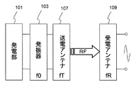
この無線電力伝送装置は、出力が並列に接続された第1の無線電力伝送部10aと第2の無線電力伝送部10bとを備えている。第1および第2の無線電力伝送部10a、10bの各々は、周波数f0のRFエネルギを出力する発振器103と、発振器103から周波数f0のRFエネルギを受け取り、送出する送電アンテナ107と、送電アンテナ107によって送出されたRFエネルギの少なくとも一部を共振磁界結合によって受け取る受電アンテナ109とを有している。
This wireless power transmission device includes a first wireless
各発振器103から出力されるRFエネルギの位相は、制御部192によって調整される。制御部192の働きにより、第1の無線電力伝送部10aにおける共振磁界195aの位相と、第2の無線電力伝送部10bにおける共振磁界195bの位相との間の差異(位相差)を所定の値に設定することができる。この無線電力伝送装置では、第1の無線電力伝送部10aにおける共振磁界195aと第2の無線電力伝送部10bにおける共振磁界195bとの間の位相差が90度以上180度以下に設定される。
The phase of the RF energy output from each
図2(a)、(b)は、いずれも、共振磁界195a、195bの位相差を模式的に示す波形図である。図2(a)に示す例では、位相差θresが90度以上180度以下の値を有していることが示されている。図2(b)は、位相差θresが180度に等しい場合における共振磁界195a、195bの波形例を示している。
FIGS. 2A and 2B are waveform diagrams schematically showing the phase difference between the resonant
本明細書では、着目する2つの共振磁界の間における位相の差異が(360×n+θ)度で表されるとき(nは整数、θは0以上360未満の実数)、θ度および(360−θ)度のうちの大きくない方の値を「位相差」と定義する。したがって、位相差の最大値は180度である。 In this specification, when the phase difference between the two resonance magnetic fields of interest is represented by (360 × n + θ) degrees (n is an integer, θ is a real number between 0 and 360), θ degrees and (360− The smaller value of θ) degrees is defined as “phase difference”. Therefore, the maximum value of the phase difference is 180 degrees.
再び図1を参照する。 Refer to FIG. 1 again.
図1では、共振磁界195aを示す点線矢印の向きと、共振磁界195bを示す点線矢印の向きが反対である。このことは、位相差が180度であることを模式的に表している。
In FIG. 1, the direction of the dotted arrow indicating the resonant
図1に示す制御部192は、例えば、対応する発振器103の発振開始のタイミングを規定するスイッチングパルスを生成する複数のパルス生成器と、これらのパルス生成器の動作を制御する制御部とを有していている。制御部192の構成例については、後述する。
The
図1の無線電力伝送装置では、第1および第2の無線電力伝送部10a、10bが並列に配置され、受電アンテナ109の受電したRFエネルギが合成部199で合成される。その結果、この無線電力伝送システムからは、合成されたRFエネルギが出力されて負荷133aに与えられる。
In the wireless power transmission apparatus of FIG. 1, the first and second wireless
第1および第2の無線電力伝送部10a、10bから出力されたRFエネルギが合成部199で合成されるとき、位相差がゼロであることが好ましい。図1の例では、各受電アンテナ109から合成部199までの伝送線路距離(線路長)を調節することにより、合成部199における位相を一致させている。
When the RF energy output from the first and second wireless
図3は、図1の無線電力伝送装置の改変例を示す図である。図1の構成と異なる点は、受電アンテナ109と合成部199との間に位相調整部135が挿入されている点にある。位相調整部135は、第1および第2の無線電力伝送部10a、10bにおける受電アンテナ109から出力されたRFエネルギの少なくとも一方の位相を進めるか遅らせることにより、合成部199での位相を一致させる回路を備えている。このような回路は、例えばキャパシタ素子およびインダクタ素子を有するリアクタンス調整回路であり得る。
FIG. 3 is a diagram illustrating a modification of the wireless power transmission device in FIG. 1. A difference from the configuration of FIG. 1 is that a
図4は、図1の無線電力伝送装置の他の改変例を示す図である。図1の構成と異なる点は、第1および第2の無線電力伝送部10a、10bから出力されるRFエネルギを伝送する2本の配線の接続を反転させている点にある。RFエネルギを有線で伝送する場合、2本の配線の組み合わせからなる一対の配線対構成が必要である。一方の配線に電流が流れるとき、もう一方の配線には戻り電流が流れており、両配線における電流の位相は逆転している。よって、第1および第2の無線電力伝送部10a、10bにおける受電アンテナ109から出力されたRFエネルギの位相差が180度である場合、第1の無線電力伝送部10aにおける受電アンテナ109と第2の無線電力伝送部10bにおける受電アンテナ109に接続されている配線対の極性の組み合わせを反対に違えれば、第1の無線電力伝送部10aにおける受電アンテナ109が受電したRFエネルギと第2の無線電力伝送部10bにおける受電アンテナ109が受電したRFエネルギの合成部199での位相を一致させることができる。
FIG. 4 is a diagram illustrating another modification of the wireless power transmission device of FIG. The difference from the configuration of FIG. 1 is that the connection of two wires that transmit RF energy output from the first and second wireless
実用的には、受電アンテナ109から出力されるRFエネルギの位相差が厳密に180度である必要はない。隣接する受電アンテナ間距離dが伝送周波数波長λに対して数度以内の電気長範囲に収まる条件では、図4の構成が有利である。例えば、1m間隔での太陽光発電モジュールの配置を想定した場合、伝送周波数が1MHzならば、伝送周波数における波長λは300mであり、dは1.2度の電気長に相当する。このような場合、図3の構成よりも簡単な図4の構成の採用が好ましい。
Practically, the phase difference of the RF energy output from the
なお、本発明の無線電力伝送装置に含まれる無線電力伝送部の個数は2つに限定されず、3つ以上であってもよい。送電アンテナ107と受電アンテナ109とによって形成されるアンテナ対の個数が3以上である場合、最近接するアンテナ対の間で位相差が90度以上180度以下となるように発振器103の発振状態を制御することが好ましい。
Note that the number of wireless power transmission units included in the wireless power transmission device of the present invention is not limited to two, and may be three or more. When the number of antenna pairs formed by the
次に、図5および図6を参照しながら、第1および第2の無線電力伝送部10a、10bにおける無線電力伝送の基本的な原理を説明する。第1および第2の無線電力伝送部10a、10bの基本構成は同一である。
Next, the basic principle of wireless power transmission in the first and second wireless
まず、図5を参照する。図5は、図1の無線電力伝送装置の構成例を示すブロックである。無線電力伝送部10a、10bは、それぞれ、発振周波数f0の発振器103と、共振周波数fTの送電アンテナと、共振周波数fRの受電アンテナ109とを備えており、共振周波数fTおよび共振周波数fRは、いずれも、周波数f0に等しく設定されている。周波数f0は、例えば50Hz〜300GHz、より好ましくは10kHz〜6GHz、さらに好ましくは20kHz〜20MHzに設定される。なお、用途によっては、20kHz〜100kHz、あるいは、13.56MHzや2.45GHzに設定される。
First, referring to FIG. FIG. 5 is a block diagram illustrating a configuration example of the wireless power transmission device in FIG. 1. Each of the wireless
発振器103は、直流エネルギ(電力)を受け取り、この直流エネルギを周波数f0のRFエネルギに変換する(DC−RF変換)。発振器103の発振状態は、発振器駆動回路190によって制御される。
The
発振器駆動回路190は、例えば、発振器103の発振のタイミングを規定するパルス信号を生成するパルス生成回路であり得る。発振器駆動回路190から発振器103に入力されるパルス信号は、典型的には矩形の波形を有するアナログ信号である。このパルス信号は、発振器103の中に含まれる大電力用トランジスタをスイッチングする駆動信号である。この駆動信号の波形が歪まないように、発振器駆動回路190と発振器103とは近接して配置されることが好ましい。なお、本実施形態では、発振器駆動回路190と発振器103とが別々の回路に分かれているが、発振器駆動回路190は、発振器103と一体化されていてもよい。
The
各発振器103から出力されるRFエネルギの位相は、発振器駆動回路190から入力されるパルス信号の入力タイミングによって規定される。ここで、第1の無線電力伝送部10aの発振器103から出力されるRFエネルギ193aの位相を「θta」、第2の無線電力伝送部10bの発振器103から出力されるRFエネルギ193bの位相を「θtb」とする。また、第1の無線電力伝送部10aの共振磁界195aの位相を「θresa」、第2の無線電力伝送部10bにおける共振磁界195bの位相を「θresb」と称する。更に、第1の無線電力伝送部10aにおける受電アンテナ109から出力されるRFエネルギ197aの位相を「θra」、第2の無線電力伝送部10bにおける受電アンテナ109から出力されるRFエネルギ197bの位相を「θrb」と称する。
The phase of the RF energy output from each
個々の発振器駆動回路190の動作は、制御部192によって調整される。制御部192は、個々の発振器駆動回路190が生成するパルス信号の生成タイミングを調整し、それによって第1の無線電力伝送部10aの発振器103から出力されるRFエネルギ193aの位相θtaと、第2の無線電力伝送部10bの発振器103から出力されるRFエネルギ193bの位相θtbとの差異を90度以上180度以下の値に設定することができる。
The operation of each
制御部192と複数の発振器駆動回路190との間では、好適にはデジタル信号からなる制御信号の伝達が行われるため、両者は離れていてもよい。制御部192と複数の発振器駆動回路190との接続は、有線によっても可能であるが、無線通信によって接続されることが好ましい。このように、制御部192は、複数の発振器駆動回路190から、それぞれ、対応する発振器に駆動信号を入力するタイミングを調整する同期調整部として機能する。
Between the
発振器103から出力されたRFエネルギ193a、193bは、それぞれ、発振器103に接続された送電アンテナ107に入力される。共振周波数が等しくなるように設計された送電アンテナ107および受電アンテナ109は、互いの共振器が形成する共振磁界の重なりによって回路的に結合し、受電アンテナ109は、送電アンテナ107によって送出されたRFエネルギの少なくとも一部を受け取ることができる。受電アンテナ109は、送電アンテナ107に接触しておらず、送電アンテナ107から例えば数mm〜数m程度の距離は離間している。
本発明の無線電力伝送装置における「アンテナ」は、共振器の電磁界の近接成分(エバネッセント・テール)を利用した結合を利用して2つの物体間でエネルギ伝送を行うための構成要素である。共振磁界を利用した無線電力伝送によれば、電磁波を遠方に伝播させるときに生じるエネルギ損失が生じないため、極めて高い効率で電力を伝送することが可能になる。このような共振磁界の結合を利用したエネルギ伝送では、ファラデーの電磁誘導の法則を利用した公知の無線電力伝送に比べて損失が少ない。また、本発明のある実施形態では、例えば数メートルも離れた2つの共振器(アンテナ)間でエネルギを伝送することが可能になる。 The “antenna” in the wireless power transmission device of the present invention is a component for performing energy transmission between two objects using coupling using a proximity component (evanescent tail) of the electromagnetic field of the resonator. According to wireless power transmission using a resonant magnetic field, energy loss that occurs when electromagnetic waves are propagated far away does not occur, so that power can be transmitted with extremely high efficiency. In energy transmission using such a coupling of resonant magnetic fields, there is less loss compared to known wireless power transmission using Faraday's law of electromagnetic induction. Moreover, in an embodiment of the present invention, energy can be transmitted between two resonators (antennas) separated by several meters, for example.
このような原理に基づく無線電力伝送を行うには、2つの共振アンテナ対の間で磁気共振による結合を生じさせる必要がある。上述のように、本発明における共振周波数fTおよび共振周波数fRは、いずれも、発振器103の周波数f0に等しく設定されるが、厳密に周波数f0に等しく設定される必要はなく、実質的に等しく設定されていれば良い。fTおよびfRのいずれも、周波数f0と完全に一致する必要は無い。共振器間の結合に基づき高効率なエネルギ伝送を実現するためには、fT=fRが理想的であるが、fTとfRとの差異が充分に小さければよい。本明細書において、「周波数fTが周波数fRに等しい」とは、以下の式1が満足される場合であると定義する。
(式1) |fT−fR|≦fT/QT+fR/QR
ここで、QTは送電アンテナの共振器としてのQ値、QRは受電アンテナの共振器としてのQ値である。一般に、共振周波数をX、共振器のQ値をQxとした場合、この共振器の共振が生じる帯域はX/Qxに相当する。|fT−fR|≦fT/QT+fR/QRの関係が設立すれば、2つの共振器間で磁気共振によるエネルギ伝送が実現する。In order to perform wireless power transmission based on such a principle, it is necessary to cause coupling by magnetic resonance between two resonant antenna pairs. As described above, the resonance frequency fT and the resonance frequency fR in the present invention are both set equal to the frequency f0 of the
(Formula 1) | fT−fR | ≦ fT / QT + fR / QR
Here, QT is a Q value as a resonator of the power transmitting antenna, and QR is a Q value as a resonator of the power receiving antenna. Generally, when the resonance frequency is X and the Q value of the resonator is Qx, the band in which the resonance of the resonator occurs corresponds to X / Qx. If a relationship of | fT−fR | ≦ fT / QT + fR / QR is established, energy transfer by magnetic resonance is realized between the two resonators.
図6は、送電アンテナ107および受電アンテナ109の等価回路を示す図である。本発明における送電アンテナ107は、送電インダクタ107aおよび第1容量素子107bが直列に接続された直列共振回路であり、受電アンテナ109は、受電インダクタ109aおよび第2容量素子109bが並列に接続された並列共振回路である。なお、送電アンテナ107の直列共振回路は寄生抵抗成分R1を有し、受電アンテナ109の並列共振回路は寄生抵抗成分R2を有している。
FIG. 6 is a diagram showing an equivalent circuit of the
本発明では、発振器103の昇圧比をVoc、送電インダクタ107aのインダクタンスをL1、受電インダクタ109aのインダクタンスをL2、送電アンテナ107と受電アンテナ109との結合係数をkとするとき、以下の関係が満足するようにL1、L2、k、Vocの値が決定されている。
(L2/L1)≧4(k/Voc)2 In the present invention, when the step-up ratio of the
(L2 / L1) ≧ 4 (k / Voc) 2
上記の関係を満足するとき、無線電力伝送を経ることで、出力されるRFエネルギの電圧を入力される直流エネルギの電圧に対して2倍以上に高めること(昇圧比:2以上)が可能になる。このような昇圧が実現する理由については、後に詳しく説明する。なお、今後、昇圧比とはシステム内における該当回路ブロック(複数の回路ブロックが接続された回路ブロック群も含む)における入出力エネルギの電圧比として定義する。例えば、直流電圧(Vdc)が交流電圧(実効電圧Vac)に上昇したとき、昇圧比はVac/Vdcである。なお、回路ブロックは、発振部103、送電アンテナ107、受電アンテナ109、後述する発電部101および整流器115などの要素である。
When the above relationship is satisfied, it is possible to increase the output RF energy voltage more than twice the input DC energy voltage (step-up ratio: 2 or more) through wireless power transmission. Become. The reason why such boosting is realized will be described in detail later. In the future, the step-up ratio will be defined as the voltage ratio of input / output energy in a corresponding circuit block (including a circuit block group to which a plurality of circuit blocks are connected) in the system. For example, when the DC voltage (Vdc) rises to the AC voltage (effective voltage Vac), the step-up ratio is Vac / Vdc. The circuit block is an element such as the
本発明の無線電力伝送装置によれば、低電圧のエネルギ(電力)を伝送時に効率的に昇圧することができる。 According to the wireless power transmission device of the present invention, low voltage energy (power) can be efficiently boosted during transmission.
次に、本発明による発電装置の構成例を説明する。図7は、本発明における発電装置の模式図である。図8は、本発明による発電装置の構成の一部を示している。 Next, a configuration example of the power generator according to the present invention will be described. FIG. 7 is a schematic diagram of a power generator according to the present invention. FIG. 8 shows a part of the configuration of the power generator according to the present invention.
図7の発電装置は、第1の発電ユニット131aと第2の発電ユニット131bとを有している。この発電装置は、各発電ユニット131a、131bが発振器103に直流エネルギを供給する発電部(発電デバイス)101を備えている点で、図1に示される無線電力伝送装置とは異なっているが、その他の構成は、図1に示す構成と同様である。
The power generation device in FIG. 7 includes a first
本発明の発電装置によれば、発電部101の出力電圧が低い場合でも、昇圧効果により、高電圧の電力を出力することが可能である。したがって、本発明の発電装置によれば、例えば太陽電池(セル)から構成された発電部(太陽光発電部)が生成する低電圧のエネルギ(電力)を伝送時に効率的に昇圧することができる。このため、直列に接続されるべきセルの個数を大幅に低減することが可能になる。その結果、敷設費用や維持費用を低減できる、普及に適した新しい太陽光発電装置を提供することが可能になる。
According to the power generation device of the present invention, even when the output voltage of the
図9は、本発明による無線電力伝送装置を備えた発電装置の使用例を示す模式図である。図示されている発電装置は、建物200の外部(屋外)に設置された発電部101と、建物200の内部に存在する電子機器に電力を伝送するための無線伝送部105とを備えている。この例における発電部101は、太陽光によって発電を行うため、以下も、太陽光発電部101と称する場合がある。ただし、本発明の発電部は、太陽光発電部に限定されない。
FIG. 9 is a schematic diagram illustrating an example of use of a power generation device including a wireless power transmission device according to the present invention. The illustrated power generation apparatus includes a
太陽光発電部101は、発電デバイスとして、接続された複数の太陽電池を有している。無線伝送部105は、建物200の壁111を介して対向する送電アンテナ107と受電アンテナ109とを有している。送電アンテナ107は、屋外の太陽光発電部101に接続されており、受電アンテナ109は屋内の電子機器に接続されている。なお、太陽光発電部101は、屋根に設置される必要は無く、建物200の壁111上に設置されても良いし、他の建物に設置されていても良い。
The solar
図9の例では、受電アンテナ109が建物200の内側に配置されているが、受電アンテナ109の位置は、この例に限定されない。送電アンテナ107および受電アンテナ109によって形成される共振アンテナ対の全体が建物200の外側(屋根または壁面)に設置されてもよい。その場合、受電アンテナ109が受け取ったRFエネルギは建物200の内部に有線または無線によって送られ得る。
In the example of FIG. 9, the
本発明における発電部を構成する発電デバイスは太陽電池に限定されず、他の発電デバイスであってもよい。例えば、発電部は燃料電池を有していても良い。燃料電池は、比較的に低い電圧のDCエネルギを出力し、高電圧系統と連結して用いられるため、本発明の昇圧効果は有用である。 The power generation device constituting the power generation unit in the present invention is not limited to the solar battery, and may be another power generation device. For example, the power generation unit may have a fuel cell. Since the fuel cell outputs DC energy having a relatively low voltage and is used in connection with a high voltage system, the boosting effect of the present invention is useful.
図10は、本発明による他の無線電力伝送装置の構成の一部を示す図である。この無線電力伝送装置が前述の無線電力伝送装置(図6)と異なる点は、受電アンテナ109に接続された整流回路(整流器)115を備えている点にある。この整流回路115の働きにより、無線電力伝送装置から直流エネルギを出力させることが可能になる。図11は、このタイプの無線電力伝送装置を備える本発明の発電装置の構成の一部を示している。図11の発電装置によれば、低電圧の直流エネルギを出力する発電部101を用いても、無線電力伝送時の昇圧効果により、充分に高い電圧に昇圧された直流エネルギを出力することができる。
FIG. 10 is a diagram showing a part of the configuration of another wireless power transmission apparatus according to the present invention. The wireless power transmission device is different from the above-described wireless power transmission device (FIG. 6) in that a rectifier circuit (rectifier) 115 connected to the
なお、整流回路115の昇圧比をVrrとすると、受電アンテナ109に整流回路115が接続されている場合には、以下の関係を満足するときに2倍以上の昇圧を実現することが可能になる。
(L2/L1)≧4(k/(Voc×Vrr))2
この点についても、詳細な説明は後述する。Note that when the boosting ratio of the
(L2 / L1) ≧ 4 (k / (Voc × Vrr)) 2
A detailed description of this point will be described later.
受電アンテナ109が受け取ったRFエネルギは、直流ではなく交流に変換されてもよい。
The RF energy received by the
以下、図面を参照しながら、本発明の好ましい実施形態を説明する。 Hereinafter, preferred embodiments of the present invention will be described with reference to the drawings.
(実施形態1)
まず、図12および図13を参照しながら、本発明による発電装置の第1の実施形態を説明する。図12は、本実施形態を示す透視模式図であり、図13は、図12に示す無線伝送部105の等価回路図である。図12、図13において、図5、図6に示した構成要素に対応する構成要素には同じ参照符号を付している。(Embodiment 1)
First, a first embodiment of a power generator according to the present invention will be described with reference to FIGS. 12 and 13. FIG. 12 is a perspective schematic diagram showing the present embodiment, and FIG. 13 is an equivalent circuit diagram of the
本実施形態の発電装置は、図7に示すように、出力が並列に接続された複数の発電ユニットを有し、各発電ユニットは、図12に示すように、発電部101と、発振器103と、無線伝送部105とが直列に接続された構成を有している。
As shown in FIG. 7, the power generation apparatus of the present embodiment includes a plurality of power generation units whose outputs are connected in parallel. Each power generation unit includes a
本実施形態における発電部101は、直列に接続された複数の太陽電池(セル)を有している。太陽電池としては、発電効率向上の観点から、結晶シリコン系の太陽光発電素子を用いることが好ましい。しかし、本発明に使用可能な太陽電池は、ガリウム砒素、CIS系などの化合物半導体材料を用いた各種の太陽光発電素子であってもよいし、有機材料を用いた各種の太陽光発電素子であってもよい。また、使用する半導体の結晶構造は、単結晶、多結晶、アモルファスのいずれであってもよい。各種半導体材料を積層したタンデム型の太陽光発電素子を利用してもよい。
The
発振器103には、D級、E級、F級などの、高効率且つ低歪な特性を実現できる増幅器を用いることができるし、ドハーティ増幅器を用いてもよい。歪成分を含む出力信号を発生するスイッチング素子の後段に、低域通過フィルタまたは帯域通過フィルタを配置することにより、高効率な正弦波を生成してもよい。
As the
無線伝送部105は、送電アンテナ107と受電アンテナ109とを有している。伝送効率の観点から、送電アンテナ107および受電アンテナ109は、対向するように配置されることが好ましい。ただし、アンテナ107、109の配置は、対向配置に限定されず、両者が直交しないように配置されていればよい。
The
発電部101によって生成された直流エネルギは、発振器103でRFエネルギに高い効率で変換される。このRFエネルギは、無線伝送部105により、空間(壁111) を介して非接触に無線によって伝送され、出力端子119から出力される。
The direct current energy generated by the
図示されている送電アンテナ107は、送電インダクタ107aおよび第1容量素子107bからなる直列共振回路であり、受電アンテナ109は受電インダクタ109aおよび第2容量素子109bからなる並列共振回路である。送電アンテナ107の共振周波数fTおよび受電アンテナ109の共振周波数fRは、それぞれ、発振器103によって生成されるRFエネルギの周波数f0にほぼ等しくなるよう設定されている。また、本実施形態における受電アンテナ109の出力インピーダンスZoutは、発振器103の入力直流インピーダンスZidcよりも高い値に設定されている。
The illustrated
前述した原理により、本実施形態では、送電アンテナ107と受電アンテナ109との距離を例えば数mm〜数mの距離に設定することができ、両者の間に壁111が存在しても、高い効率でエネルギを伝送できる。なお、送電アンテナ107と受電アンテナ109との間に壁111が存在せず、単なる空間が存在する場合でも、非接触でエネルギを伝送できることは言うまでもない。
Based on the principle described above, in this embodiment, the distance between the
また、本実施形態では、このような無線による非接触接続を実現できるだけではなく、送電アンテナ107に流入するRFエネルギの入力電圧に対して、受電アンテナ109の側で昇圧されたRFエネルギとして取り出すことが可能となる。
Further, in the present embodiment, not only such wireless non-contact connection can be realized, but also the RF energy boosted on the
回路ブロック間でのRFエネルギの多重反射を抑圧し、総合発電効率を改善するためには、受電アンテナ109の出力端子が負荷に接続された状態において、発振器103の出力インピ−ダンスZocと送電アンテナ107の入力インピーダンスZinとを等しくすることが好ましい。また、同様に、発振器103が送電アンテナ107に接続された状態で、受電アンテナの出力インピーダンスZoutが、接続される負荷の抵抗値Rと等しくすることが好ましい。
In order to suppress multiple reflections of RF energy between circuit blocks and improve the overall power generation efficiency, the output impedance Zoc of the
なお、本明細書において、2つのインピーダンスが「等しい」とは、インピーダンスが厳密に一致する場合に限られず、ほぼ等しい場合を含み、具体的には、2つのインピーダンスの差異が、大きい方のインピーダンスの25%以下である場合を含むものと定義する。 In the present specification, the phrase “two impedances are“ equal ”” is not limited to the case where the impedances are exactly the same, but includes the case where the two impedances are substantially equal. It is defined to include the case of 25% or less.
送電アンテナ107と受電アンテナ109との間は、壁111が存在する必要はなく、障害物を介することなく送電アンテナ107と受電アンテナ109とが対向していてもよい。また、送電アンテナ107と受電アンテナ109とを隔てるものが屋根であってもかまわない。
There is no need for the
なお、送電アンテナ107および受電アンテナ109の両方が屋内に配置されていてもよいし、屋外に配置されていてもよい。このような場合でも、2つのアンテナ間で無線電力伝送を行う際に昇圧を行うことができる。送電アンテナ107および受電アンテナ109の両方が屋内に設置されている場合、屋外の太陽光発電部101と送電アンテナ107との接続は、例えば建物200の壁111に設けた開口部を介した有線によって実現され得る。また、送電アンテナ107および受電アンテナ109の両方が屋外に設置されている場合、屋内の電子機器と受電アンテナ109との接続も、例えば建物200の壁111に設けた開口部を介した有線によって実現され得る。屋内外の有線接続を省略するためには、図12に示す例のように、送電アンテナ107を屋外に設置し、受電アンテナ109を屋内に設置することが好ましい。
Note that both the
本実施形態における無線電力伝送の効率は、送電アンテナ107と受電アンテナ109との間隔(アンテナ間隔)や、送電アンテナ107と受電アンテナ109を構成する回路素子の損失の大きさに依存する。なお、「アンテナ間隔」とは、実質的に2つのインダクタ107a、109aの間隔である。アンテナ間隔は、アンテナの配置領域(アンテナにによって占有される領域)の大きさを基準に評価することができる。
The efficiency of wireless power transmission in the present embodiment depends on the distance between the
好ましい実施形態において、送電インダクタ107aおよび受電インダクタ109aは、いずれも、平面状に広がり、両者は互いに平行に対向するように配置される。ここで、アンテナの配置領域の大きさとは、サイズが相対的に小さなアンテナの配置領域の大きさを意味し、アンテナを構成するインダクタの外形が円形の場合は円の直径、正方形の場合は正方形の一辺の長さ、長方形の場合は長方形の短辺の長さに定義されるものとする。本実施形態によれば、アンテナ間隔が、アンテナの配置領域の大きさの1.5倍程度であっても、90%以上の無線伝送効率でエネルギを伝送することが可能である。また、無線伝送部105の出力インピーダンスを入力インピーダンスに対して7832倍以上に増大させることも可能である。
In a preferred embodiment, the
本実施形態における送電インダクタ107aおよび受電インダクタ109aは、それぞれ、巻数N1、N2のスパイラル構造を有している(N1>1、N2>1)が、巻数が1のループ構造を有していてもよい。これらのインダクタ107a、109aは、一層の導電体パターンから構成されている必要は無く、積層された複数の導電体パターンを直列に接続した構成を有していてもよい。
The
送電インダクタ107a、受電インダクタ109aは、良好な導電率を有する銅や銀などの導電体から好適に形成され得る。RFエネルギの高周波電流は、導電体の表面を集中して流れるため、発電効率を高めるため、導電体の表面を高導電率材料で被覆してもよい。導電体の断面中央に空洞を有する構成からインダクタ107a、109aを形成すると、軽量化を実現することができる。更に、リッツ線などの並列配線構造を採用してインダクタ107a、109aを形成すれば、単位長さ辺りの導体損失を低減できるため、直列共振回路、および並列共振回路のQ値を向上させることができ、より高い効率で電力伝送が可能になる。
The
製造コストを抑制するために、インク印刷技術を用いて、配線を一括して形成することも可能である。送電インダクタ107aおよび/または受電インダクタ109aの周辺に磁性体を配置してもよいが、送電インダクタ107aと受電インダクタ109aとの結合係数を極端に高い値に設定することは好ましくない。このため、インダクタ107a、109aの間の結合係数を適度な値に設定できる空芯スパイラル構造を有するインダクタを用いることがより好ましい。
In order to suppress the manufacturing cost, it is also possible to form the wirings at a time using an ink printing technique. Although a magnetic body may be arranged around the
各インダクタは、一般的にはコイル形状を有している。しかし、そのような形状に限定されない。高周波では、ある程度の線長をもつ導体は、インダクタンスをもつため、インダクタとして機能する。また、他の例として、ビーズ状のフェライトに導線を通しただけのものでもインダクタとして機能する。 Each inductor generally has a coil shape. However, it is not limited to such a shape. At high frequencies, a conductor having a certain line length has an inductance and functions as an inductor. As another example, a bead-like ferrite simply passed through a conducting wire functions as an inductor.
第1、第2容量素子107b、109bには、例えばチップ形状、リード形状を有する、あらゆるタイプのキャパシタを利用できる。空気を介した2配線間の容量を第1、第2容量素子107b、109bとして機能させることも可能である。第1、第2容量素子107b、109bをMIMキャパシタから構成する場合は、公知の半導体プロセスまたは多層基板プロセスを用いて低損失の容量回路を形成できる。
For the first and
長期信頼性の確保という観点から、送電アンテナ107および受電アンテナ109を構成する部品(インダクタおよび容量素子など)は保護装置117内に格納されることが好ましい。また、保護装置117内には防水加工が施されることが好ましい。
From the viewpoint of ensuring long-term reliability, it is preferable that components (such as an inductor and a capacitive element) constituting the
伝送損失を最小化するためには、送電アンテナ107および受電アンテナ109は、できるだけ近接して配置されることが好ましい。ただし、昇圧比を所望の値に調整する目的で保護装置117内における位置を調整してもよい。
In order to minimize transmission loss, the
保護装置117は、壁111や屋根などの外部部材に直接に固定されていてもよい。送電アンテナ107と受電アンテナ109との磁界結合の強さに影響を与えない範囲で、保護装置117および外部部材にそれぞれ強磁性体および磁石を設けることにより、強磁性体と磁石との間に働く磁力を利用し、保護装置117を外部部材に着脱自在に取り付けるようにしてもよい。あるいは、保護装置117および外部部材のいずれか一方に吸盤を設けることにより、保護装置117を外部部材に着脱自在に取り付けるようにしてもよい。
The
次に、図13を参照しながら、本発明の発電装置によって得られる昇圧効果を説明する。 Next, the boosting effect obtained by the power generator of the present invention will be described with reference to FIG.
ここでは、送電側の送電アンテナ107と受電側の受電アンテナ109とが結合係数kで結合しているものとする。結合係数は、同一周波数f0で共振する2つの共振器(アンテナ107、109)を近接させた際に分離する2つの共振周波数fL、fHを計測することにより、以下の式から導かられる。
(式2) k=(fH2−fL2)/(fH2+fL2)Here, it is assumed that the
(Equation 2) k = (fH 2 -fL 2) / (
なお、発振器103の周波数f0は、共振周波数fL、fHの近傍に設定することが好ましい。より詳しくは、共振周波数fL、fHにおける結合共振器対のQ値を、それぞれ、QL、QHとするとき、以下の式3を満たすようにf0を設定することが好ましい。
(式3)fL−fL/QL≦f0≦fH+fH/QHThe frequency f0 of the
(Formula 3) fL−fL / QL ≦ f0 ≦ fH + fH / QH
また、インダクタンスL1の送電インダクタ107aとインダクタンスL2の受電インダクタ109aとの間に生じる相互インダクタンスMと結合係数kとの間には、以下の関係が成立する。
(式4) M=k×(L1×L2)0.5 Further, the following relationship is established between the mutual inductance M generated between the
(Formula 4) M = k × (L1 × L2) 0.5
このように、結合係数kは、インダクタ間または共振器間の結合強度の指標として従来から用いられている公知の結合係数と同一の指標である。結合係数kは、0<k<1の関係を満たす数値である。従来の電磁誘導によるエネルギ伝送では、結合係数kを可能な限り大きく、ほぼ1に等しくなるように、インダクタ対の構成および配置関係が設計される。後述するように、本発明では、結合係数kを1に近い値に設定する必要はなく、0.5以下の値に設定することも可能である。
Thus, the coupling coefficient k is the same index as a known coupling coefficient conventionally used as an index of coupling strength between inductors or resonators. The coupling coefficient k is a numerical value that satisfies the
受電アンテナ109の並列型共振回路において、受電インダクタ109aを流れる高周波電流をIL2、第2容量素子109bを流れる高周波電流をIC2とすると、図13に示す向きに流れる出力高周波電流I2は、以下の式によって表される。
(式5) I2=−IL2−IC2In the parallel resonance circuit of the
(Formula 5) I2 = -IL2-IC2
また、送電インダクタ107aを流れる高周波電流をIL1とすると、受電インダクタ109aを流れる高周波電流IL2、第2容量素子109bを流れる高周波電流IC2、受電インダクタ109aのインダクタンスL2、受電インダクタ109aの寄生抵抗R2、送電インダクタ107aのインダクタンスL1、第2容量素子109bのキャパシタンスC2を用いて、以下の式が導かれる。
(式6) (R2+jωL2)×IL2+jωM×IL1=IC2/(jωC2)If the high-frequency current flowing through the
(Expression 6) (R2 + jωL2) × IL2 + jωM × IL1 = IC2 / (jωC2)
受電アンテナ109では共振条件が成立しているため、以下の(式7)が成立している。
(式7) ωL2=1/(ωC2)Since the resonance condition is satisfied in the
(Expression 7) ωL2 = 1 / (ωC2)
上記の(式5)〜(式7)から、以下の式が成立する。
(式8) R2×IL2+jωM×IL1=jωL2×I2From the above (Formula 5) to (Formula 7), the following formula is established.
(Expression 8) R2 × IL2 + jωM × IL1 = jωL2 × I2
(式8)を変形して以下の式を得る。
(式9) I2=k×(L1/L2)0.5×IL1−j(R2/ωL2)×IL2(Expression 8) is modified to obtain the following expression.
(Formula 9) I2 = k × (L1 / L2) 0.5 × IL1-j (R2 / ωL2) × IL2
一方、送電アンテナ107の共振器の低損失性を評価する指標Q値は、(式10)の式によって表される。
(式10) Q2=ωL2/R2On the other hand, the index Q value for evaluating the low loss property of the resonator of the
(Formula 10) Q2 = ωL2 / R2
ここで、共振器のQ値が非常に高い場合、(式6)の右辺第2項を無視する近似が成り立つ。よって、最終的に、以下の(式11)により、受電アンテナ109で生じる高周波電流(出力電流)I2の大きさが導出される。
(式11) I2=k×(L1/L2)0.5×IL1
ここで、高周波電流I2は、送電側の共振器(送電アンテナ107)に入力される高周波電流I1(=送電インダクタ107aを流れる高周波電流IL1)、共振器(アンテナ)間の結合係数k、送電インダクタ107aおよび受電インダクタ109aのインダクタンスL1、L2に依存する。Here, when the Q value of the resonator is very high, an approximation that ignores the second term on the right side of (Equation 6) holds. Therefore, finally, the magnitude of the high-frequency current (output current) I2 generated in the
(Formula 11) I2 = k × (L1 / L2) 0.5 × IL1
Here, the high-frequency current I2 is the high-frequency current I1 (= high-frequency current IL1 flowing through the
上記の(式11)から、本実施形態の発電装置の昇流比Irは、次の(式12)によって表される。
(式12) Ir=|I2/I1|/Voc=k/Voc×(L1/L2)0.5 From the above (Formula 11), the ascending ratio Ir of the power generator of this embodiment is expressed by the following (Formula 12).
(Formula 12) Ir = | I2 / I1 | / Voc = k / Voc × (L1 / L2) 0.5
また、昇圧比Vrおよびインピーダンス変換比Zrは、それぞれ、(式13)および(式14)によって表される。
(式13) Vr=(Voc/k)×(L2/L1)0.5
(式14) Zr=(Voc/k)2×(L2/L1)Further, the boost ratio Vr and the impedance conversion ratio Zr are expressed by (Expression 13) and (Expression 14), respectively.
(Formula 13) Vr = (Voc / k) × (L2 / L1) 0.5
(Formula 14) Zr = (Voc / k) 2 × (L2 / L1)
(式13)からわかるように、(L2/L1)>(k/Voc)2の条件が成立するとき、昇圧比Vrは1よりも大きくなる。このことから、結合係数kが小さくなると、昇圧比Vrが上昇することがわかる。従来の電磁誘導によるエネルギ伝送では、結合係数kを低下させることは、伝送効率の大幅な低下につながっていたが、本発明の磁気共振方式では、結合係数kを低下させても伝送効率の大幅な低下には至らない。特に、送電アンテナ107および受電アンテナ109の各々を構成する共振器のQ値を高い値に設定すれば、昇圧比Vrを増大させながら、伝送効率の低下を抑制することが可能である。As can be seen from (Expression 13), when the condition of (L2 / L1)> (k / Voc) 2 is satisfied, the step-up ratio Vr is greater than 1. This shows that the step-up ratio Vr increases as the coupling coefficient k decreases. In conventional energy transmission by electromagnetic induction, reducing the coupling coefficient k has led to a significant reduction in transmission efficiency. However, in the magnetic resonance system of the present invention, the transmission efficiency is greatly increased even if the coupling coefficient k is reduced. It does not lead to a significant decline. In particular, if the Q value of the resonator constituting each of the
太陽光発電システムにおけるパーシャルシェイディングの影響を回避するためには、多数の太陽光発電部を直列に接続する構成よりも、複数の太陽光発電部を並列に接続する構成を採用することが好ましい。2つの太陽光発電部を直列に接続する場合と同等の電圧特性を、2つの太陽光発電部を並列に接続することによって得るためには、各太陽光発電部の出力電圧を2倍に昇圧する必要がある。 In order to avoid the influence of partial shading in the photovoltaic power generation system, it is preferable to adopt a configuration in which a plurality of photovoltaic power generation units are connected in parallel rather than a configuration in which a large number of photovoltaic power generation units are connected in series. . In order to obtain the same voltage characteristics as when two solar power generation units are connected in series by connecting the two solar power generation units in parallel, the output voltage of each solar power generation unit is boosted twice. There is a need to.
(式12)から、昇圧比Vrが2に等しくなるのは、(L2/L1)≧4×(k/Voc)2の関係が満足されるときである。本発明では、(L2/L1)≧4×(k/Voc)2の関係が満足されるため、2以上の昇圧比Vrが実現できる。From (Equation 12), the step-up ratio Vr is equal to 2 when the relationship of (L2 / L1) ≧ 4 × (k / Voc) 2 is satisfied. In the present invention, since the relationship of (L2 / L1) ≧ 4 × (k / Voc) 2 is satisfied, a boost ratio Vr of 2 or more can be realized.
(L2/L1)≧100×(k/Voc)2の関係が成立すると、10倍以上の昇圧比Vrを実現することができる。(L2/L1)≧10000×(k/Voc)2の関係が成立すると、100倍以上の昇圧比Vrを実現することができる。When the relationship of (L2 / L1) ≧ 100 × (k / Voc) 2 is established, a boost ratio Vr of 10 times or more can be realized. When the relationship of (L2 / L1) ≧ 10000 × (k / Voc) 2 is established, a step-up ratio Vr of 100 times or more can be realized.
本実施形態の発電部では、このように高い昇圧比Vrを実現するように、k、Voc、L2、L1の大きさを設定することは容易である。 In the power generation unit of the present embodiment, it is easy to set the sizes of k, Voc, L2, and L1 so as to realize such a high boost ratio Vr.
以下、本実施形態の無線電力伝送装置の効果を従来の無線電力伝送装置と比較しながら説明する。 Hereinafter, the effect of the wireless power transmission device of the present embodiment will be described in comparison with a conventional wireless power transmission device.
特許文献2に開示されている無線電力伝送装置では、2つの磁気共振器の間でエネルギが伝送されるが、その無線電力伝送装置は、2つの共振器で同一の共振回路構成を採用しているため、伝送に際して昇圧効果が発現しない。本発明の無線電力伝送装置によって得られる出力電圧の上昇効果は、送電アンテナの側に直列共振構造を採用するとともに、受電アンテナの側に並列共振構造を採用し、これらの異なる共振構造の間でエネルギの伝送が行われたときに生じる新規な効果である。
In the wireless power transmission device disclosed in
なお、直列共振回路や並列共振回路は、RFタグに代表される従来の無線通信システムでも使用され得る。しかし、無線通信システムの高周波ブロックの特性試験に用いる測定器の測定端子の終端インピーダンスや高周波ケーブルの特性インピーダンスは、基本的に50Ωに設定されている。よって、無線通信システムのアンテナとの接続点では、送信機器内でも受信機器内でも、インピーダンスを50Ωにあわせて回路ブロック間を接続するのが一般的である。 Note that the series resonant circuit and the parallel resonant circuit can also be used in a conventional wireless communication system represented by an RF tag. However, the termination impedance of the measurement terminal of the measuring instrument used for the high frequency block characteristic test of the wireless communication system and the high frequency cable characteristic impedance are basically set to 50Ω. Therefore, at the connection point with the antenna of the wireless communication system, it is common to connect the circuit blocks in accordance with the impedance of 50Ω in both the transmitting device and the receiving device.
一方、本発明における無線伝送部での入出力インピーダンスの変換比Zrは、後述の実施例においても100を超えたり、条件によっては20000を超えていたり、と極めて高い値を示すように設定される。このような高い入出力インピーダンス変換比Zrは、従来の通信システムでは考慮の対象外である。 On the other hand, the input / output impedance conversion ratio Zr in the wireless transmission unit according to the present invention is set so as to be extremely high, such as exceeding 100 or exceeding 20000 depending on conditions in the embodiments described later. . Such a high input / output impedance conversion ratio Zr is not considered in the conventional communication system.
また、本発明では、2つの共振器(アンテナ)間の距離を大きく設定し、結合係数kを低く設定するほど、より高い昇圧比Vrを得ることができるが、このことは、公知の通信システムに用いられてきた無線伝送部の構造および機能からは容易に想到し得ない効果である。 Further, in the present invention, the higher the step-up ratio Vr can be obtained as the distance between the two resonators (antennas) is set larger and the coupling coefficient k is set lower, this is a known communication system. This is an effect that cannot easily be conceived from the structure and function of the wireless transmission unit used in the above.
なお、電源回路などに利用されるトランスでは、2つのインダクタが近接しており、一種の無線電力伝送装置として機能している。しかし、これらのインダクタ間では、磁気共振型の結合は生じていない。なお、トランスでは、送電インダクタの巻数N1に対する受電インダクタの巻数N2の比率を大きくすることにより、昇圧効果を実現することも可能である。しかし、トランス昇圧回路によって例えば10以上の昇圧比を実現しようとすると、巻数N2を巻数N1の10倍以上に増加させる必要がある。巻数N2の大幅な増加は、受電インダクタにおける寄生抵抗成分R2を比例的に上昇させるため、伝送効率の低下を招いてしまう。この点、従来のトランス技術での昇圧効果は、巻数比に対して線形的な効果に限定されるのに対して、本発明では、巻数N1と巻数N2とが同じ値に設定されていても、非線形的に高いZrを得ることができる。 In a transformer used for a power supply circuit or the like, two inductors are close to each other and function as a kind of wireless power transmission device. However, no magnetic resonance type coupling occurs between these inductors. In the transformer, it is also possible to realize a boosting effect by increasing the ratio of the number of turns N2 of the power receiving inductor to the number of turns N1 of the power transmission inductor. However, to achieve a boost ratio of, for example, 10 or more by the transformer booster circuit, it is necessary to increase the number of turns N2 to 10 times or more the number of turns N1. A large increase in the number of turns N2 causes the parasitic resistance component R2 in the power receiving inductor to increase proportionally, leading to a decrease in transmission efficiency. In this regard, the boosting effect in the conventional transformer technology is limited to a linear effect with respect to the turns ratio, whereas in the present invention, even if the turns N1 and the turns N2 are set to the same value. , Non-linearly high Zr can be obtained.
本発明では、送電インダクタ107aのインダクタンスL1と受電インダクタ109aのインダクタンスL2とを等しく設定する必要はない。例えば、インダクタンスL2をインダクタンスL1より大きく設定することにより、昇圧比Vrを高めることができる。
In the present invention, it is not necessary to set the inductance L1 of the
図14は、受電インダクタ109aのインダクタンスL2を高めるため、受電インダクタ109aの巻数N2を送電インダクタ107aの巻数N1よりも大きな値に設定した実施形態を示す図である。N2/N1が1よりも大きいと、公知のトランス昇圧回路を用いて昇圧する場合に比べ、より低い損失で高い昇圧比を実現できる。
FIG. 14 is a diagram showing an embodiment in which the number of turns N2 of the
インダクタンスL2をインダクタンスL1より大きくするために、N2/N1を1よりも大きく設定する代わりに、あるいはN2/N1を1に設定したままで、受電アンテナ109の形成領域を送電アンテナ105の形成領域よりも拡大してもよい。
Instead of setting N2 / N1 larger than 1 in order to make the inductance L2 larger than the inductance L1, or with N2 / N1 set to 1, the area where the
以下の説明において、送電インダクタ107aおよび受電インダクタ109aの少なくとも前面は、いずれも、平面的な形状を有しており、それらは互いに直交しないように配置されているものとする。図15(a)は、送電アンテナ107の配置面に対して垂直に投影した、受電アンテナ109の配置領域113を示している。ここで、送電アンテナ107の「配置面」とは、送電インダクタ107aの前面を含む1つの平面(第1配置面)であると定義する。図15(b)は、送電インダクタ107aの配置面240を示す断面図である。図15(b)の例における送電インダクタ107aは、配置面240に対して平行である。また、受電アンテナの配置領域とは、送電アンテナ107の配置面240に対して垂直に投影された受電インダクタ109aの輪郭によって囲まれた領域であると定義する。
In the following description, it is assumed that at least the front surfaces of the
図15(a)には、送電アンテナ107の配置面に対して垂直に投影された送電インダクタ107aが示されている。図15(a)に示す例では、送電アンテナ107の配置面に投影された送電インダクタ107aが、配置領域113の内部に存在し、かつ、配置領域113の縁部に寄っている。このような配置構成を採用することにより、更に高い昇圧比を実現することができる。
FIG. 15A shows a
無線伝送部105の昇圧比を調整するために、アンテナの形状およびサイズを非対称な組合せに設定した上で、受電アンテナよりも送電アンテナを大きく設定してもよい。
In order to adjust the step-up ratio of the
なお、アンテナの配置関係は図15に示す例に限定されず、送電アンテナ107と受電アンテナ109とを入れ替えた配置関係であってもよい。すなわち、図15における「送電アンテナ107」を「受電アンテナ109」に置き換え、「配置領域113」を「送電アンテナ107の配置領域」に置き換えてもよい。ここで、「送電アンテナ107の配置領域」とは、受電アンテナ109の配置面に投影されたインダクタ107aの輪郭によって囲まれた領域である。また、「受電アンテナ109の配置面」とは、受電インダクタ109aの前面を含む1つの平面(第2配置面)であると定義する。伝送効率の観点から、第1配置面と第2配置面とは互いに平行な関係にあることが好ましいが、両者は厳密に平行である必要は無い。なお、送電インダクタ107a、受電インダクタ109aは、平面的な形状を有している必要はない。
Note that the antenna arrangement relationship is not limited to the example illustrated in FIG. 15, and may be an arrangement relationship in which the
以下、本発明の発電装置の好ましい実施形態を説明する。 Hereinafter, preferred embodiments of the power generator of the present invention will be described.
まず、図16を参照する。図16に示す発電装置の実施形態は、各々が、発電部101、発振器103、送電アンテナ107及び受電アンテナ109を含む複数の発電ユニット131a、131b、・・・、131nを備えている。複数の受電アンテナ109が受電した出力エネルギは並列に合成されて総出力エネルギを形成する。送電アンテナ107と受電アンテナ109とを含む共振アンテナ対において形成される共振磁界195は、隣接するアンテナ対の間で、位相差の絶対値θres(=|θresa−θresb|)が90度以上180度以下、好ましくは180度となるよう設定される。
First, referring to FIG. 16 includes a plurality of
本実施形態では、例えば、第1の発電ユニット131aにおける発振器駆動回路190によって、対応する発振器103から送出されるRFエネルギ193aの位相θtaが制御される。同様に、第2の発電ユニット131bにおける発振器駆動回路190によって、対応する発振器103から送出されるRFエネルギ193bの位相θtbが制御される。図5を参照しながら説明したように、各発振器駆動回路190は有線または無線により、制御部192(図5)と接続されている。
In the present embodiment, for example, the phase θta of the
第1の発電ユニット131a内における発振器103から出力されたRFエネルギ193a、および、第2の発電ユニット131b内における発振器103から出力されたRFエネルギ193bは、いずれも、同一周波数f0の高周波エネルギである。上記制御により、RFエネルギ193aとRFエネルギ193bの位相差の絶対値θt(=|θta−θtb|)を制御する。θresを上述の範囲内にするには、θtを、90度以上180度以下、好ましくは180度となるよう制御する。
The
各発電ユニット131a、131bにおける送電アンテナ107のインダクタンス、サイズ、巻数を等しく設定することにより、θtをθresと等しく設定することができる。第1の発電ユニット131a内における受電アンテナ109から出力されるRFエネルギ197aの位相θraと第2の発電ユニット内におけるRFエネルギ197bの位相θrbが最終的に同相となるよう、図3および図4を参照しながら説明した構成を採用することが好ましい。
By setting the inductance, size, and number of turns of the
共振磁界195a、195bの位相差の絶対値θresが90度以上180度以下になれば、2つの共振磁界195a、195bのベクトル成分の少なくとも一部が相殺しあうため、周辺空間への電磁漏洩が低減できる。また、θresが180度になれば、2つの共振磁界が相殺しあうため、周辺空間への電磁漏洩が抑圧できる。この効果は、波長に対して遥かに短い(一般的に周波数f0の波長の1/8、好ましくは1/16以下とされる)磁界源対に対して有効であり、その抑圧効果は、磁界源対間距離が短いほど有効である。よって本発明の発電装置内に3以上の共振アンテナ対が存在する場合、最も隣接する共振アンテナ対間についてθresを90度以上、より好ましくは180度に設定すると、電磁漏洩抑圧効果が向上する。
If the absolute value θres of the phase difference between the resonance
本発明の発電装置内にN個(Nは4以上の整数)の共振アンテナ対が存在する場合、Nが偶数であるときは、N/2個の隣接共振アンテナ対組についてθresを90度以上180度以下、より好ましくは180度に設定することが、装置からの総電磁漏洩の抑圧効果を最大化する条件である。また、Nが奇数であるときも、(N−1)/2個の隣接共振アンテナ対組についてθresを90度以上180度以下、より好ましくは180度に設定することが、装置からの総電磁漏洩の抑圧効果を最大化する条件である。 When N (N is an integer of 4 or more) resonant antenna pairs are present in the power generation device of the present invention, when N is an even number, θres is 90 degrees or more for N / 2 adjacent resonant antenna pairs. Setting to 180 degrees or less, more preferably 180 degrees is a condition for maximizing the effect of suppressing the total electromagnetic leakage from the apparatus. In addition, even when N is an odd number, it is possible to set θres to 90 degrees or more and 180 degrees or less, and more preferably 180 degrees for (N−1) / 2 adjacent resonant antenna pair pairs. This is a condition that maximizes the suppression effect of leakage.
図17は、本発明の発電装置内に4対の送受共振アンテナ対141a〜141dが正方格子配置で存在する場合の上面模式図である。この場合には、中心間の距離がd3である送受共振アンテナ対141aと送受共振アンテナ対141dよりも、中心間の距離がd1(<d3)である送受共振アンテナ対141aと送受共振アンテナ対141b、および中心間の距離がd2(<d3)である送受共振アンテナ対141aと送受共振アンテナ対141cがθres≧90度を満たすことが好ましい。これは、相殺する磁界成分間の距離が短いほど、周辺への漏洩電磁成分が低減できるからである。よって、本発明の発電装置内においては、図18に示すように、最近接する送受共振アンテナ対間で磁界抑圧条件(90度≦θres≧180度)を満足させることが好ましい。図18において、「+」の符号は同じ位相を有する共振磁界を示し、「−」の符号は、「+」の符号の共振磁界に対して90度以上180度以下の範囲で位相が異なる共振磁界を示している。
FIG. 17 is a schematic top view when four pairs of transmitting and receiving
(実施形態2)
次に、図19を参照しながら、本発明による発電装置の第2の実施形態を説明する。(Embodiment 2)
Next, a second embodiment of the power generator according to the present invention will be described with reference to FIG.
本実施形態の発電装置が第1実施形態における発電装置と異なる第1の点は、合成部199より後段で、RFエネルギをDCエネルギに変換する整流回路115を直列に接続している点にある。このような構成を採用することにより、複数の受電アンテナ109が受電した受電エネルギをDCエネルギとして出力することができる。
The first point of difference between the power generation apparatus of the present embodiment and the power generation apparatus of the first embodiment is that a
本実施形態の発電装置によっても、第1の実施形態における発電装置の効果と同様の効果を得ることができ、更に、直流の電力を出力として得ることができる。 Also by the power generation device of this embodiment, the same effect as that of the power generation device in the first embodiment can be obtained, and further, DC power can be obtained as an output.
回路ブロック間でのRFエネルギの多重反射を抑圧し、総合発電効率を改善するためには、整流回路115の出力端子が不図示の直流負荷または直流負荷システムに接続された状態において、発振器103の出力インピ−ダンスZocと送電アンテナ107の入力インピーダンスZinとをほぼ等しくすることが好ましい。また、同様に、発振器103が送電アンテナ107に接続された状態で、整流回路115の出力インピーダンスZroutが、接続される不図示の直流負荷または直流負荷システムの抵抗値Rにほぼ等しく設定されることが好ましい。
In order to suppress multiple reflections of RF energy between circuit blocks and improve the overall power generation efficiency, the output terminal of the
整流回路115には様々な方式で整流を行う回路があり、両波整流やブリッジ整流回路を利用できる。図20(a)は、半波倍電圧整流回路の回路図であり、図20(b)は両波倍電圧整流回路の回路図である。他にも、3倍以上の昇圧比を実現できる高倍圧整流回路方式がある。これらの整流回路は、いずれも、本発明に適用可能である。
The
図20に例示される倍電圧整流回路を用いれば、整流回路115に入力されるRF電圧の2倍に昇圧した直流電圧を出力させることが可能となる。このような整流回路115を用いると、無線伝送部105での昇圧効果に加えて、更なる昇圧効果を実現することが可能になる。
If the voltage doubler rectifier circuit illustrated in FIG. 20 is used, a DC voltage boosted to twice the RF voltage input to the
本実施形態では、実施形態1について導出した昇圧比Vrおよびインピーダンス変換比Zrが、それぞれ、整流回路115における昇圧比Vrrを用いて、以下の(式15)、(式16)へと書き換えられる。
(式15) Vr=(Voc×Vrr/k)×(L2/L1)0.5
(式16) Zr=(Voc×Vrr/k)2×(L2/L1)In the present embodiment, the boost ratio Vr and the impedance conversion ratio Zr derived for the first embodiment are rewritten into the following (Expression 15) and (Expression 16) using the boost ratio Vrr in the
(Formula 15) Vr = (Voc × Vrr / k) × (L2 / L1) 0.5
(Formula 16) Zr = (Voc × Vrr / k) 2 × (L2 / L1)
本実施形態では、上記の(式15)からわかるように、(L2/L1)>(k/(Voc×Vrr))2の関係を満足する場合に昇圧比を1より大きくすることが可能になる。In this embodiment, as can be seen from the above (Formula 15), the step-up ratio can be made larger than 1 when the relationship of (L2 / L1)> (k / (Voc × Vrr)) 2 is satisfied. Become.
昇圧比Vrを2以上にするためには、(L2/L1)≧4×(k/(Voc×Vrr))2での関係を満足する必要がある。(L2/L1)≧100×(k/(Voc×Vrr))2の関係が成立するとき、10倍以上の昇圧比Vrを実現することができる。In order to increase the boost ratio Vr to 2 or more, it is necessary to satisfy the relationship of (L2 / L1) ≧ 4 × (k / (Voc × Vrr)) 2 . When the relationship of (L2 / L1) ≧ 100 × (k / (Voc × Vrr)) 2 is established, a boost ratio Vr of 10 times or more can be realized.
本実施形態の発電装置によれば、直流給電システムを実現できる。直流給電システムの一例として、24Vdcでの給電システムが検討されているが、(L2/L1)=2304×(k/(Voc×Vrr))2の関係を満たすことにより、0.5Vから24Vまで48倍の昇圧を実現できる。このため、本発明を直流給電システムに適用する場合は、(L2/L1)≧2304×(k/(Voc×Vrr))2の関係を満足することが好ましい。また、(L2/L1)≧10000×(k/(Voc×Vrr))2の関係が成立すると、100倍以上の昇圧比Vrを達成することができる。According to the power generation device of this embodiment, a DC power feeding system can be realized. As an example of a DC power supply system, a power supply system at 24 Vdc has been studied, but by satisfying the relationship of (L2 / L1) = 2304 × (k / (Voc × Vrr)) 2 , from 0.5 V to 24 V A boost of 48 times can be realized. Therefore, when the present invention is applied to a DC power supply system, it is preferable to satisfy the relationship of (L2 / L1) ≧ 2304 × (k / (Voc × Vrr)) 2 . Further, when the relationship of (L2 / L1) ≧ 10000 × (k / (Voc × Vrr)) 2 is established, a boost ratio Vr of 100 times or more can be achieved.
(実施形態3)
次に、図21を参照しながら、本発明による発電装置の実施形態を説明する。図21は、本実施形態における発電装置のブロック図である。図21において、前述の実施形態における発電装置の構成要素と同一の構成要素には、同一の参照符号を付しており、その詳細な説明は省略する。(Embodiment 3)
Next, an embodiment of the power generator according to the present invention will be described with reference to FIG. FIG. 21 is a block diagram of the power generation device according to this embodiment. In FIG. 21, the same reference numerals are given to the same components as those of the power generation device in the above-described embodiment, and the detailed description thereof is omitted.
図21の発電装置は、並列的に接続された複数の発電ユニット131a、131b・・・131nを含んでいる。本実施形態における発電ユニット131a〜131nは、いずれも、実施形態2の発電装置であるが、本発明の効果を得るには、並列に接続された少なくとも2つの発電装置が本発明の発電装置であればよい。
21 includes a plurality of
各発電ユニット131a〜131nは、直列に接続された太陽光発電部101、発振器103、送電アンテナ107、受電アンテナ109、および整流回路115を備えている。
Each of the
太陽光発電部101によって生成された直流エネルギは、発振器103でRFエネルギに高い効率で変換される。このRFエネルギは、送電側の送電アンテナ107と受電側の受電アンテナ109との間で非接触に転送された後、整流回路115によって直流エネルギに変換され、各発電ユニット131a〜131nから出力された直流エネルギ(電力)は、並列接続によって加算された後、負荷133aに供給される。
The direct current energy generated by the photovoltaic
本実施形態によれば、発電ユニット131a〜131nの各々から得られる出力電圧が、個々の太陽光発電部によって得られる出力電圧よりも飛躍的に増大している。よって、発電ユニット131a〜131nを並列に接続しても、負荷133aが要求する電圧値により近い値を実現することが可能である。
According to the present embodiment, the output voltage obtained from each of the
発電ユニット131a〜131nが並列に接続されているため、発電ユニット131a〜131nの一部の特性が劣化した場合や、発電ユニット131a〜131nに対する太陽光の照射条件に差異が生じた場合でも、従来の発電装置よりも安定した特性を得ることが可能となる。
Since the
負荷133aは、例えば、一般の電気機器や蓄電池である。負荷133aは、直流を交流へ変換するためのインバータ機能回路、昇降圧機能回路、または両機能の複合機能を持つパワーコンディショナ回路であってもよい。例えば負荷133aのインピーダンスと整合させるため、本実施形態における発電装置の一部で発電装置が直列に接続されていてもよい。
The
(実施形態4)
次に、図22を参照しながら、本発明による発電装置の第4の実施形態を説明する。(Embodiment 4)
Next, a fourth embodiment of the power generator according to the present invention will be described with reference to FIG.
本実施形態の発電装置が第2実施形態における発電装置と異なる第1の点は、合成部199より後段で、RFエネルギをACエネルギに変換する周波数変換回路189を直列に接続し、複数の受電アンテナ109が受電した受電エネルギをACエネルギとして出力する点にある。
The first point that the power generation device of the present embodiment is different from the power generation device in the second embodiment is that a
本実施形態の発電装置によっても、第1の実施形態における発電装置の効果と同様の効果を得ることができ、さらに負荷/系統133bへ送出可能な交流電力を出力として得ることができる。ここで、負荷/系統133bとは、後述するように、ACエネルギで駆動可能な負荷、またはACエネルギを送電する電力系統の少なくとも一方を意味する。本実施形態によれば、要求に応じて、ACエネルギを負荷へ出力する場合と系統へ出力する場合とを切り替えることも可能である。
Also with the power generation device of the present embodiment, the same effect as that of the power generation device in the first embodiment can be obtained, and AC power that can be sent to the load /
回路ブロック間でのRFエネルギの多重反射を抑圧し、総合発電効率を改善するためには、周波数変換回路189の出力端子が交流負荷または交流系統システムに接続された状態において、発振器103の出力インピ−ダンスZocと送電アンテナ107の入力インピーダンスZinとをほぼ等しくすることが好ましい。
In order to suppress multiple reflections of RF energy between circuit blocks and improve the overall power generation efficiency, the output impedance of the
周波数変換回路189には様々な方式の回路があるが、マトリックスコンバータ方式のように直接周波数変換を行う構成や、間接周波数変換を行う回路が採用できる。また、出力構成として、単相や三相などの出力に対応した周波数変換回路技術は、いずれも、本発明に適用可能である。
There are various types of circuits for the
本実施形態では、実施形態1について導出した昇圧比Vrおよびインピーダンス変換比Zrが、それぞれ、周波数変換回路189における昇圧比Vconを用いて、以下の(式17)、(式18)へと書き換えられる。
(式17) Vr=(Voc×Vcon/k)×(L2/L1)0.5
(式18) Zr=(Voc×Vcon/k)2×(L2/L1)In the present embodiment, the boost ratio Vr and the impedance conversion ratio Zr derived for the first embodiment are rewritten into the following (Expression 17) and (Expression 18) using the boost ratio Vcon in the
(Expression 17) Vr = (Voc × Vcon / k) × (L2 / L1) 0.5
(Formula 18) Zr = (Voc × Vcon / k) 2 × (L2 / L1)
本実施形態では、上記の(式17)からわかるように、(L2/L1)>(k/(Voc×Vcon))2の関係を満足する場合に昇圧比を1より大きくすることが可能になる。In this embodiment, as can be seen from the above (Equation 17), the step-up ratio can be made larger than 1 when the relationship of (L2 / L1)> (k / (Voc × Vcon)) 2 is satisfied. Become.
昇圧比Vrを2以上にするためには、(L2/L1)≧4×(k/(Voc×Vcon))2での関係を満足する必要がある。(L2/L1)≧100×(k/(Voc×Vcon))2の関係が成立するとき、10倍以上の昇圧比Vrを実現することができる。In order to increase the boost ratio Vr to 2 or more, it is necessary to satisfy the relationship of (L2 / L1) ≧ 4 × (k / (Voc × Vcon)) 2 . When the relationship of (L2 / L1) ≧ 100 × (k / (Voc × Vcon)) 2 is established, a boost ratio Vr of 10 times or more can be realized.
本実施形態の発電装置によれば、系統接続発電装置を実現できる。発電部の電圧をVinとした場合、Vout=Vin×(Voc×Vcon/k)×(L2/L1)0.5が出力電圧となる。系統システムの一例として、202V系システム(202V±20V)が存在しているが、182≦Vout≦222を満足することにより、低電圧な発電部出力エネルギを系統接続することが可能となる。According to the power generator of this embodiment, a system connection power generator can be realized. When the voltage of the power generation unit is Vin, Vout = Vin × (Voc × Vcon / k) × (L2 / L1) 0.5 is the output voltage. As an example of the system, there is a 202V system (202V ± 20V). However, when 182 ≦ Vout ≦ 222 is satisfied, it is possible to connect the low-voltage power generation unit output energy to the system.
なお、周波数変換回路189には、昇降圧機能を備えることも可能である。
Note that the
(実施形態5)
次に、図23を参照しながら、本発明による発電装置の実施形態を説明する。図23は、本実施形態における発電装置のブロック図である。図23において、前述の実施形態における発電装置の構成要素と同一の構成要素には、同一の参照符号を付しており、その詳細な説明は省略する。(Embodiment 5)
Next, an embodiment of the power generator according to the present invention will be described with reference to FIG. FIG. 23 is a block diagram of the power generation device in the present embodiment. In FIG. 23, the same reference numerals are given to the same components as those of the power generation device in the above-described embodiment, and the detailed description thereof is omitted.
図23の発電装置は、並列的に接続された複数の発電ユニット131a、131b・・・131nを含んでいる。本発明の効果を得るには、並列に接続された少なくとも2つの発電装置が本発明の発電装置であればよい。
23 includes a plurality of
各発電ユニット131a〜131nは、直列に接続された太陽光発電部101、発振器103、送電アンテナ107、受電アンテナ109、および周波数変換回路189を備えている。
Each of the
太陽光発電部101によって生成された直流エネルギは、発振器103でRFエネルギに高い効率で変換される。このRFエネルギは、送電側の送電アンテナ107と受電側の受電アンテナ109との間で非接触に転送された後、周波数変換回路189によって交流エネルギに変換され、各発電ユニット131a〜131nから出力された交流エネルギ(電力)は、並列接続によって加算された後、負荷133aに供給される。
The direct current energy generated by the photovoltaic
本実施形態によれば、発電ユニット131a〜131nの各々から得られる出力電圧が、個々の太陽光発電部によって得られる出力電圧よりも飛躍的に増大している。よって、発電ユニット131a〜131nを並列に接続しても、負荷133aが要求する電圧値により近い値を実現することが可能である。
According to the present embodiment, the output voltage obtained from each of the
発電ユニット131a〜131nが並列に接続されているため、発電ユニット131a〜131nの一部の特性が劣化した場合や、発電ユニット131a〜131nに対する太陽光の照射条件に差異が生じた場合でも、従来の発電装置よりも安定した特性を得ることが可能となる。
Since the
負荷/系統133bは、例えば、交流入力に対応した一般の電気機器や蓄電池である。負荷/系統133bは、昇降圧機能回路を備えることが出来る。例えば負荷/系統133bのインピーダンスと整合させるため、本実施形態における発電装置の一部で発電装置が直列に接続されていてもよい。
The load /
(実施例1)
本発明の発電装置では、複数の発電ユニットが並列に接続される。そして、個々の発電ユニットにおける無線電力伝送によって昇圧を行うことができる。このため、最初に1つの発電ユニットの実施例を説明し、その後、複数の発電ユニットを備える発電装置の実施例を説明する。Example 1
In the power generator of the present invention, a plurality of power generation units are connected in parallel. And pressure | voltage rise can be performed by the wireless power transmission in each electric power generation unit. For this reason, the Example of one electric power generation unit is described first, and the Example of an electric power generating apparatus provided with a several electric power generation unit is described after that.
以下、本発明の実施例1を説明する。
まず、受光面側の形状が一辺12cmの正方形である9つの単結晶シリコン系太陽光発電素子(セル)を直列に接続し、出力電圧4.5V、出力電流1A、出力インピーダンス4.5Ωの太陽光発電部を作製した。この太陽光発電部の出力端子に、出力周波数が3MHz、出力インピーダンスZocが5Ωの発振器を接続した。F級増幅器により実現した発振器の効率は95%であった。実施例1における発振器の昇圧比Zocは1.05である。 First, nine single crystal silicon solar power generation elements (cells) having a square shape with a side of 12 cm on the side of the light receiving surface are connected in series, and a solar having an output voltage of 4.5 V, an output current of 1 A, and an output impedance of 4.5Ω. A photovoltaic unit was produced. An oscillator having an output frequency of 3 MHz and an output impedance Zoc of 5Ω was connected to the output terminal of the solar power generation unit. The efficiency of the oscillator realized by the class F amplifier was 95%. The step-up ratio Zoc of the oscillator in the first embodiment is 1.05.
送電アンテナおよび受電アンテナは、その共振周波数が発振器の出力周波数に等しい3MHzとなるように設計した。送電アンテナは、インダクタンスが1.988μHの送電インダクタとキャパシタンスが830pFの第1容量素子とを直列に接続することによって作製した。受電アンテナは、インダクタンスが1.988μHの受電インダクタとキャパシタンスが830pFの第2容量素子とを並列に接続して作製した。第1および受電インダクタは、共に、直径80μmの銅配線を30本ずつ互いに絶縁して並列に配置して構成したリッツ線により実現した。2つのインダクタの外形は共に一辺36cmの正方形であり、巻数は2に設定した。各アンテナ(共振器)のQ値は1350であった。 The power transmission antenna and the power reception antenna were designed so that the resonance frequency was 3 MHz, which is equal to the output frequency of the oscillator. The power transmission antenna was manufactured by connecting a power transmission inductor having an inductance of 1.988 μH and a first capacitor element having a capacitance of 830 pF in series. The power receiving antenna was manufactured by connecting a power receiving inductor having an inductance of 1.988 μH and a second capacitor element having a capacitance of 830 pF in parallel. Both the first and power receiving inductors were realized by litz wires configured by arranging 30 parallel copper wires each having a diameter of 80 μm and arranging them in parallel. The outer shape of the two inductors was a square with a side of 36 cm, and the number of turns was set to two. The Q value of each antenna (resonator) was 1350.
送電アンテナと受電アンテナは、互いの形成面を平行に対向して配置し、対抗面間の間隔はg(cm)とした。この間隔gを5cmから75cmまでの範囲で変化させながら、各g値に対する共振器間の無線伝送効率を最大とする最適な入出力インピーダンスZinとZoutを測定した。実際の測定は、以下の2段階の手順で行った。 The power transmitting antenna and the power receiving antenna were disposed so that their formation surfaces face each other in parallel, and the distance between the opposing surfaces was g (cm). While changing the gap g in the range from 5 cm to 75 cm, optimum input / output impedances Zin and Zout that maximize the wireless transmission efficiency between the resonators for each g value were measured. Actual measurement was performed by the following two-step procedure.
第1に、2つのアンテナ(共振器)の入出力端子間の高周波特性を、50Ωの端子インピーダンスのネットワークアナライザにて測定し、50Ωを基準インピーダンスとする測定データを得た。 First, high-frequency characteristics between the input and output terminals of two antennas (resonators) were measured with a network analyzer having a terminal impedance of 50Ω, and measurement data having 50Ω as a reference impedance were obtained.
第2に、上記測定データを基に、端子での信号反射が最小化するような入出力端子のインピーダンス条件Zin、Zoutを回路シミュレータ上で導出した。 Second, based on the measurement data, impedance conditions Zin and Zout of the input / output terminals that minimize signal reflection at the terminals are derived on a circuit simulator.
図24は、導出したZinおよびZoutのg依存性を示すグラフである。図25は、無線伝送部の入出力インピーダンス変換比Zrおよび伝送効率のg依存性を示すグラフである。 FIG. 24 is a graph showing g dependence of derived Zin and Zout. FIG. 25 is a graph showing the dependency of the input / output impedance conversion ratio Zr and transmission efficiency on the wireless transmission unit on g.
Zrの値は、間隔gの全範囲で1を超えており、間隔gが大きくなるほど、Zrが飛躍的に増大することがわかった。より詳しく説明すると、g=5cmでZrは7.7であり、g=7.5cmでZrは20.6、g=75cmでは23158に達した。 The value of Zr exceeded 1 in the entire range of the interval g, and it was found that Zr increased dramatically as the interval g increased. More specifically, g = 5 cm, Zr was 7.7, g = 7.5 cm, Zr was 20.6, and g = 75 cm, reaching 23158.
また、g=5mmでの共振器間の結合係数kは0.376であり、(式14)においてVocを1として無線伝送部のみのkを導出した場合(=0.361)と比較して4%の誤差しかなかった。以上の結果より、(式14)の妥当性が証明された。 In addition, the coupling coefficient k between the resonators when g = 5 mm is 0.376, compared with the case where k of only the wireless transmission unit is derived by setting Voc to 1 in (Equation 14) (= 0.361). There was only an error of 4%. From the above results, the validity of (Equation 14) was proved.
図26は、図25のグラフにおける10cm≦g≦40cmの範囲での特性を拡大して示したグラフである。例えば、一般的な建物において壁の厚さは、10cmから30cm程度の範囲である。この範囲内に間隔gが含まれるとき、20〜363という非常に大きいZrが得られた。なお、g=22.5の条件で得られた147という高いZr値は、従来のトランス技術によって得るためには、一次コイルの巻数に対する二次コイルの巻数の比を12.1倍に設定する必要がある。本発明の実施例では、巻数比1の送電アンテナおよび受電アンテナを用いながら、Zrを147まで飛躍的に高めることができた。 FIG. 26 is a graph showing enlarged characteristics in the range of 10 cm ≦ g ≦ 40 cm in the graph of FIG. For example, in a typical building, the wall thickness is in the range of about 10 cm to 30 cm. When the gap g was included in this range, a very large Zr of 20 to 363 was obtained. In order to obtain the high Zr value of 147 obtained under the condition of g = 22.5 by the conventional transformer technique, the ratio of the number of turns of the secondary coil to the number of turns of the primary coil is set to 12.1 times. There is a need. In the example of the present invention, Zr could be dramatically increased to 147 while using a power transmission antenna and a power reception antenna with a turns ratio of 1.
上記の方法で導出した入出力インピーダンスZin、Zoutに、入出力端子インピーダンスを整合させた場合の順方向通過特性は、本発明による発電装置の発電ユニット内での無線伝送効率に相当する。図26に示されるように、g=22.5cmでも、98.3%という良好な無線伝送効率を得ることができた。 The forward pass characteristics when the input / output terminal impedances are matched with the input / output impedances Zin and Zout derived by the above method correspond to the wireless transmission efficiency in the power generation unit of the power generation apparatus according to the present invention. As shown in FIG. 26, good wireless transmission efficiency of 98.3% could be obtained even with g = 22.5 cm.
無線伝送部に前述の発振器を接続することにより、入力直流電圧から効率93.1%でRF出力を得ることが実現した。入力直流電圧に対する出力RF実効電圧の昇圧比は12.7であった。入力された電力の一部は、回路ブロック間のわずかな不整合に起因する損失により、熱に変わったものと考えられる。 By connecting the aforementioned oscillator to the wireless transmission unit, it was possible to obtain an RF output with an efficiency of 93.1% from the input DC voltage. The step-up ratio of the output RF effective voltage to the input DC voltage was 12.7. It is considered that a part of the input electric power is changed to heat due to a loss due to a slight mismatch between circuit blocks.
次に、上述した実施例1の構成と同じ構成を有する2つの発電ユニットを用意し、これらの出力を並列に接続した。具体的には、2つの送電アンテナの重心間、及び2つの受電アンテナの重心間の距離がそれぞれ50cmとなるよう、平行移動して並列に配置した。2つの受電アンテナが受電したエネルギは、並列に合成された。 Next, two power generation units having the same configuration as that of Example 1 described above were prepared, and their outputs were connected in parallel. Specifically, the distance between the centroids of the two power transmission antennas and the distance between the centroids of the two power reception antennas were respectively moved in parallel and arranged in parallel. The energy received by the two power receiving antennas was synthesized in parallel.
実施例1aでは、2つの発振器の出力の位相差を90度から180度まで30度ずつずらして測定を行い、それぞれ実施例1a−90、1a−120、・・・1a−180とした。一方、比較例1では、2つの発振器の出力の位相差をゼロ度から60度までの値とし、比較例1−0、1−30、1−60とした。2つの発電ユニットにおける送電インダクタの配線は同一方向に回転して形成した。実施例1a、及び比較例1における漏洩電磁界評価指標として5m離れた地点での近傍界強度を導出した。 In Example 1a, measurement was performed by shifting the phase difference between the outputs of the two oscillators by 30 degrees from 90 degrees to 180 degrees, and Examples 1a-90, 1a-120,. On the other hand, in Comparative Example 1, the phase difference between the outputs of the two oscillators was set to a value from zero degrees to 60 degrees, and Comparative Examples 1-0, 1-30, and 1-60 were used. The wiring of the power transmission inductor in the two power generation units was formed by rotating in the same direction. As a leakage electromagnetic field evaluation index in Example 1a and Comparative Example 1, the near-field strength at a point 5 m away was derived.
(比較例a〜c)
実施例1の場合と同様に、無線伝送部を送受共に共振周波数3MHzの共振器で実現した比較例a、bを作製した。実施例1と比較例a、bとの間にある相違点は、比較例a、bにおける2つのアンテナ(共振器)の共振方式を相互に等しくした点のみにある。すなわち、比較例aでは、2つのアンテナをそれぞれLC直列型共振器から構成し、比較例bでは、2つのアンテナをそれぞれLC並列共振器から構成した。各共振器の回路定数は、実施例1における回路定数と一致させた。更に、2つのアンテナが共振しないように構成された比較例cも作製した。なお、比較例a〜cは、昇圧効果と高効率動作の両立が出来なかったため、2つの発電ユニットの並列動作や近傍界測定は行わなかった。(Comparative Examples a to c)
As in the case of Example 1, comparative examples a and b in which the wireless transmission unit was realized by a resonator having a resonance frequency of 3 MHz for both transmission and reception were produced. The only difference between Example 1 and Comparative Examples a and b is that the resonance methods of the two antennas (resonators) in Comparative Examples a and b are equal to each other. That is, in Comparative Example a, each of the two antennas is composed of an LC series resonator, and in Comparative Example b, each of the two antennas is composed of an LC parallel resonator. The circuit constant of each resonator was matched with the circuit constant in Example 1. Further, a comparative example c configured so that the two antennas do not resonate was also produced. In Comparative Examples a to c, the boosting effect and the high-efficiency operation could not be achieved at the same time, so the parallel operation of the two power generation units and the near-field measurement were not performed.
以下の表1は、実施例1、比較例a〜cにおける共振器の構成や、g=22.5cmの無線伝送部特性などを示している。 Table 1 below shows the configuration of the resonators in Example 1 and Comparative Examples a to c, the characteristics of the wireless transmission unit at g = 22.5 cm, and the like.

表1から明らかなように、実施例1ではワイヤレスでの高効率電力伝送を実現しつつ、極めて高い昇圧比Vrを達成できることが明らかとなった。 As is clear from Table 1, it was found that Example 1 can achieve a very high step-up ratio Vr while realizing high-efficiency power transmission wirelessly.
また、表2は、実施例1a、比較例1における近傍界強度を示している。なお、近傍界強度については、10度刻みで全立体角方向で測定を行った後、最悪値を示した方向での強度を示している。 Table 2 shows the near-field intensity in Example 1a and Comparative Example 1. In addition, about the near-field intensity | strength, after measuring in all the solid angle directions by 10 degree | times, the intensity | strength in the direction which showed the worst value is shown.
表2から明らかなように、θresが90度以上180度以下となる本発明の構成は、ワイヤレスでの高効率電力伝送を実現しつつ、極めて高い昇圧比Vrを達成できるだけでなく周辺空間への電磁漏洩を効果的に抑圧できることが実証された。 As is apparent from Table 2, the configuration of the present invention in which θres is 90 degrees or more and 180 degrees or less not only achieves a very high step-up ratio Vr while realizing high-efficiency power transmission wirelessly, It has been demonstrated that electromagnetic leakage can be effectively suppressed.
(実施例2)
次に、実施例2として、実施例1における受電アンテナの構成と同一の構成を有する受電アンテナの出力に、倍電圧整流回路を接続した発電ユニットを作製した。作製した半波倍電圧整流回路の直流変換効率は、共振周波数3MHzにおいて、93.4%を示した。導入した整流回路では、入力高周波電圧に対して出力直流電圧が2倍の値となる昇圧比Vrr=2の昇圧機能が得られ、太陽光発電部の出力エネルギに対して、本発電ユニットが出力する直流エネルギは86.4%の強度であった。(Example 2)
Next, as Example 2, a power generation unit in which a voltage doubler rectifier circuit was connected to the output of the power receiving antenna having the same configuration as that of the power receiving antenna in Example 1 was produced. The DC conversion efficiency of the produced half-wave voltage doubler rectifier circuit was 93.4% at a resonance frequency of 3 MHz. In the introduced rectifier circuit, a step-up function with a step-up ratio Vrr = 2 in which the output DC voltage is twice the input high-frequency voltage is obtained, and the power generation unit outputs the output energy of the solar power generation unit. The direct current energy was 86.4% intensity.
次に、上述した実施例2の構成と同じ構成を有する2つの発電ユニットを用意し、これらの出力を並列に接続した。具体的には、2つの送電アンテナの重心間、及び2つの受電アンテナの重心間の距離がそれぞれ50cmとなるよう、平行移動して並列に配置した。2つの受電アンテナが受電したエネルギは整流回路で整流された後、並列に合成された。 Next, two power generation units having the same configuration as that of Example 2 described above were prepared, and their outputs were connected in parallel. Specifically, the distance between the centroids of the two power transmission antennas and the distance between the centroids of the two power reception antennas were respectively moved in parallel and arranged in parallel. The energy received by the two power receiving antennas was rectified by the rectifier circuit and then combined in parallel.
実施例2aでは、2つの発振器の出力の位相差を180度ずらして測定を行ったのに対し、比較例2では、2つの発振器の出力の位相差をゼロ度とした。2つの発電ユニットにおける送電インダクタの配線は同一方向に回転して形成した。10度刻みで全立体角方向の近傍界強度測定を行ったが、実施例2aの最悪値は比較例2に対し65%低い値を実現できた。 In Example 2a, measurement was performed by shifting the phase difference between the outputs of the two oscillators by 180 degrees, whereas in Comparative Example 2, the phase difference between the outputs of the two oscillators was set to zero degrees. The wiring of the power transmission inductor in the two power generation units was formed by rotating in the same direction. The near-field intensity measurement in all solid angle directions was performed in increments of 10 degrees, and the worst value of Example 2a was 65% lower than that of Comparative Example 2.
(実施例3)
実施例3として、実施例1の構成の受電アンテナ出力に、ブリッジ整流回路を接続した発電ユニットを作製した。作製したブリッジ整流回路の直流変換効率は、共振周波数3MHzにおいて、94.1%を示した。導入した整流回路では、太陽光発電部の出力エネルギに対して、本発電装置の出力直流エネルギは87.0%の強度であった。(Example 3)
As Example 3, a power generation unit in which a bridge rectifier circuit was connected to the power receiving antenna output having the configuration of Example 1 was produced. The DC conversion efficiency of the manufactured bridge rectifier circuit was 94.1% at a resonance frequency of 3 MHz. In the introduced rectifier circuit, the output DC energy of the power generation device was 87.0% of the intensity of the output energy of the photovoltaic power generation unit.
次に、上述した実施例3の構成と同じ構成を有する2つの発電ユニットを用意し、これらの出力を並列に接続した。具体的には、2つの送電アンテナの重心間、及び2つの受電アンテナの重心間の距離がそれぞれ50cmとなるよう、平行移動して並列に配置した。2つの受電アンテナが受電したエネルギは整流回路で整流された後、並列に合成された。 Next, two power generation units having the same configuration as that of Example 3 described above were prepared, and their outputs were connected in parallel. Specifically, the distance between the centroids of the two power transmission antennas and the distance between the centroids of the two power reception antennas were respectively moved in parallel and arranged in parallel. The energy received by the two power receiving antennas was rectified by the rectifier circuit and then combined in parallel.
実施例3aでは、2つの発振器の出力の位相差を180度ずらして測定を行ったのに対し、比較例3では、2つの発振器の出力の位相差をゼロ度とした。2つの発電ユニットにおける送電インダクタの配線は同一方向に回転して形成した。10度刻みで全立体角方向の近傍界強度測定を行ったが、実施例3aの最悪値は比較例3に対し66%低い値を示した。 In Example 3a, measurement was performed by shifting the phase difference between the outputs of the two oscillators by 180 degrees, whereas in Comparative Example 3, the phase difference between the outputs of the two oscillators was set to zero degrees. The wiring of the power transmission inductor in the two power generation units was formed by rotating in the same direction. The near field intensity measurement in all solid angle directions was performed in increments of 10 degrees. The worst value of Example 3a was 66% lower than that of Comparative Example 3.
(実施例4)
実施例3の条件を一部変更し、Voc=1.52、g=15cmの条件で実施例4の発電ユニットを作製した。実施例4の発電ユニットの出力電圧は308Vであり、発電効率は87.2%であった。Example 4
A part of the conditions of Example 3 was changed, and a power generation unit of Example 4 was produced under the conditions of Voc = 1.52 and g = 15 cm. The output voltage of the power generation unit of Example 4 was 308 V, and the power generation efficiency was 87.2%.
次に、上述した実施例4の構成と同じ構成を有する2つの発電ユニットを用意し、これらの出力を並列に接続した。具体的には、2つの送電アンテナの重心間、及び2つの受電アンテナの重心間の距離がそれぞれ50cmとなるよう、平行移動して並列に配置した。2つの受電アンテナが受電したエネルギは整流回路で整流された後、並列に合成された。 Next, two power generation units having the same configuration as that of Example 4 described above were prepared, and their outputs were connected in parallel. Specifically, the distance between the centroids of the two power transmission antennas and the distance between the centroids of the two power reception antennas were respectively moved in parallel and arranged in parallel. The energy received by the two power receiving antennas was rectified by the rectifier circuit and then combined in parallel.
実施例4aでは、2つの発振器の出力の位相差を180度ずらして測定を行ったのに対し、比較例4では、2つの発振器の出力の位相差をゼロ度とした。2つの発電ユニットにおける送電インダクタの配線は同一方向に回転して形成した。10度刻みで全立体角方向の近傍界強度測定を行ったが、実施例4aの最悪値は比較例4に対し63%低い値を示した。 In Example 4a, measurement was performed by shifting the phase difference between the outputs of the two oscillators by 180 degrees, whereas in Comparative Example 4, the phase difference between the outputs of the two oscillators was set to zero degrees. The wiring of the power transmission inductor in the two power generation units was formed by rotating in the same direction. The near field intensity measurement in all solid angle directions was performed in increments of 10 degrees. The worst value of Example 4a was 63% lower than that of Comparative Example 4.
(実施例5)
実施例4の発電ユニットの構成と同じ構成を有する7個の発電ユニットを一列に並べ、これら全て並列に接続し、実施例5の発電装置を作製した。この発電装置では、出力電圧308V、27.5Wの発電出力を得た。同様に、比較例5として太陽光発電セルを63個直列に接続した発電装置を作製した。以下の表2に、実施例5と比較例5の特性を示した。(Example 5)
Seven power generation units having the same configuration as that of the power generation unit of Example 4 were arranged in a line, and all of these units were connected in parallel to produce the power generation device of Example 5. With this power generation device, a power generation output with an output voltage of 308 V and 27.5 W was obtained. Similarly, as Comparative Example 5, a power generation apparatus in which 63 photovoltaic power generation cells were connected in series was manufactured. Table 2 below shows the characteristics of Example 5 and Comparative Example 5.
実施例5では、セル直列数が比較例5よりも格段に少ないにもかかわらず、出力電圧は9.8倍高い値であった。実施例5によれば、300Vでの直流給電システムに対して最適な電圧値を提供する発電装置を実現することができる。 In Example 5, the output voltage was 9.8 times higher although the number of cells in series was much smaller than that in Comparative Example 5. According to the fifth embodiment, it is possible to realize a power generator that provides an optimal voltage value for a DC power supply system at 300V.
また、実施例5では、並列配置した実施例4の発電ユニットにおいて隣接しあう3組の間で、θres=180度となるよう、発振の位相を制御した。隣接する送電アンテナの重心間、及び受電アンテナの重心間の距離は、それぞれ50cmであった。 Further, in Example 5, the oscillation phase was controlled so that θres = 180 degrees between three adjacent groups in the power generation unit of Example 4 arranged in parallel. The distance between the centroids of the adjacent power transmission antennas and the centroid of the power reception antennas were 50 cm, respectively.
一方、比較例5aでは、実施例5と同数の太陽電池セルを含みながらも、発振器、送電アンテナ、受電アンテナ、整流部を一組しかシステム内に有しない。。実施例5では、全ての発電ユニットにおける送電インダクタの配線は同一方向に回転して形成した。10度刻みで全立体角方向の近傍界強度測定を行ったが、実施例5の最悪値は比較例5aの最悪値に対し78%の低減が実現できた。 On the other hand, the comparative example 5a includes only one set of an oscillator, a power transmission antenna, a power reception antenna, and a rectification unit in the system while including the same number of solar cells as in the fifth embodiment. . In Example 5, the wiring of the power transmission inductor in all the power generation units was formed by rotating in the same direction. The near-field intensity measurement in all solid angle directions was performed in increments of 10 degrees, and the worst value of Example 5 was able to be reduced by 78% with respect to the worst value of Comparative Example 5a.
本発明は、発電装置の敷設コストを低減し、発電部の一部が劣化した時の交換作業を簡便化することを可能にする。また、本発明は、発電部の出力電圧を簡単に上昇させることができるため、出力電圧の低い発電素子(太陽電池)を直列に接続して発電部を構成する場合に、発電素子の接続個数を大幅に低減することが可能になる。このため、パーシャルシェイディングに対する特性劣化を低減し、安定した電力供給を実現する太陽光発電装置を構築できる。また、無線電力伝送部位からの漏洩電磁成分を抑圧することが可能となる。また、低電圧で出力される発電デバイスからの出力エネルギを高電圧な系統と連結して機能する発電装置である燃料電池システムにおいても、本発明の昇圧効果は有用である。 The present invention makes it possible to reduce the installation cost of the power generation device and simplify the replacement work when a part of the power generation unit deteriorates. In addition, since the present invention can easily increase the output voltage of the power generation unit, when the power generation unit is configured by connecting power generation elements (solar cells) with low output voltage in series, the number of connected power generation elements Can be greatly reduced. For this reason, it is possible to construct a photovoltaic power generation apparatus that reduces characteristic deterioration with respect to partial shading and realizes stable power supply. In addition, it is possible to suppress the leakage electromagnetic component from the wireless power transmission site. The boosting effect of the present invention is also useful in a fuel cell system that is a power generation device that functions by connecting output energy from a power generation device that is output at a low voltage to a high voltage system.
101 発電部(太陽光発電部)
103 発振器
10a 第1の無線電力伝送部
10b 第2の無線電力伝送部
105 無線伝送部
107 送電アンテナ(送電側の共振器)
107a 第1インダクタ
107b 第1キャパシタ
109 受電アンテナ(受電側の共振器)
109a 第2インダクタ
109b 第2キャパシタ
111 壁
113 送電アンテナの配置面へ投影した受電アンテナの配置領域
115 整流器
117 保護装置
119 出力端子
131a、131b・・・131n 発電ユニット
133a 負荷
133b 負荷/系統
135 位相調整回路
141 送受共振アンテナ対
141a、141b、141c、141d 送受共振アンテナ対
189 周波数変換回路
190 発振器駆動回路
192 制御部
193a、193b、・・・193n 発振器から出力されるRFエネルギ
195a、195b、・・・195n 共振磁界
197a、197b、・・・197n 受電アンテナから出力されるRFエネルギ
199 合成部101 Power generation unit (solar power generation unit)
DESCRIPTION OF
107a
109a
Claims (32)
直流エネルギを周波数f0のRFエネルギに変換する発振器と、
前記RFエネルギを送出する送電アンテナであって、共振周波数fTを有する直列共振回路を構成するように直列に接続された第1インダクタおよび第1容量素子を含む送電アンテナと、
前記送電アンテナによって送出された前記RFエネルギの少なくとも一部を共振磁界の結合によって受け取る受電アンテナであって、共振周波数fRを有する並列共振回路を構成するように並列に接続された第2インダクタおよび第2容量素子を含む受電アンテナと、を備え、
前記共振周波数fTおよび前記共振周波数fRは、前記RFエネルギの周波数f0に実質的に等しく設定され、
前記発振器に入力された前記直流エネルギの電圧に対する前記発振器から出力される前記RFエネルギの電圧の比である昇圧比をVoc、第1インダクタのインダクタンスをL1、第2インダクタのインダクタンスをL2、前記送電アンテナと前記受電アンテナとの結合係数をkとするとき、
(L2/L1)≧4(k/Voc)2を満足する、第1および第2の無線電力伝送部と、
第1および第2の無線電力伝送部における前記受電アンテナから受け取ったRFエネルギを合成して出力する合成部と、
前記第1の無線電力伝送部における前記共振磁界の位相と前記第2の無線電力伝送部における前記共振磁界の位相との位相差θresを90度以上180度以下にするように前記第1および第2の無線電力伝送部における前記発振器を制御する制御部と、
を備える無線電力伝送装置。 First and second wireless power transmission units, each of the first and second wireless power transmission units,
An oscillator that converts direct current energy into RF energy of frequency f0;
A power transmission antenna for transmitting the RF energy, the power transmission antenna including a first inductor and a first capacitance element connected in series so as to form a series resonance circuit having a resonance frequency fT;
A power receiving antenna that receives at least a part of the RF energy transmitted by the power transmitting antenna by coupling of a resonant magnetic field, and a second inductor connected in parallel to form a parallel resonant circuit having a resonant frequency fR, and a second inductor A power receiving antenna including two capacitive elements;
The resonance frequency fT and the resonance frequency fR are set substantially equal to the frequency f0 of the RF energy,
The step-up ratio, which is the ratio of the voltage of the RF energy output from the oscillator to the voltage of the DC energy input to the oscillator, is Voc, the inductance of the first inductor is L1, the inductance of the second inductor is L2, and the power transmission When the coupling coefficient between the antenna and the power receiving antenna is k,
First and second wireless power transmission units satisfying (L2 / L1) ≧ 4 (k / Voc) 2 ;
A combining unit that combines and outputs the RF energy received from the power receiving antenna in the first and second wireless power transmission units;
The first and second phase differences θres between the phase of the resonant magnetic field in the first wireless power transmission unit and the phase of the resonant magnetic field in the second wireless power transmission unit are 90 degrees or more and 180 degrees or less. A control unit for controlling the oscillator in the two wireless power transmission units;
A wireless power transmission device comprising:
直流エネルギを出力する発電部と、
前記発電部から出力された直流エネルギを周波数f0のRFエネルギに変換する発振器と、
前記RFエネルギを送出する送電アンテナであって、共振周波数fTを有する直列共振回路を構成するように直列に接続された第1インダクタおよび第1容量素子を含む送電アンテナと、
前記送電アンテナによって送出された前記RFエネルギの少なくとも一部を共振磁界の結合によって受け取る受電アンテナであって、共振周波数fRを有する並列共振回路を構成するように並列に接続された第2インダクタおよび第2容量素子を含む受電アンテナと、を備え、
前記共振周波数fTおよび前記共振周波数fRは、前記RFエネルギの周波数f0に実質的に等しく設定され、
前記発振器に入力された前記直流エネルギの電圧に対する前記発振器から出力される前記RFエネルギの電圧の比である昇圧比をVoc、第1インダクタのインダクタンスをL1、第2インダクタのインダクタンスをL2、前記送電アンテナと前記受電アンテナとの結合係数をkとするとき、
(L2/L1)≧4(k/Voc)2を満足する、第1および第2の発電ユニットと、
前記第1および第2の発電ユニットにおける前記受電アンテナから受け取ったRFエネルギを合成して出力する合成部と、
前記第1の発電ユニットにおける前記共振磁界の位相と前記第2の発電ユニットにおける前記共振磁界の位相との位相差θresを90度以上180度以下にするように前記第1および第2の発電ユニットにおける前記発振器を制御する制御部と、
を備える発電装置。 First and second power generation units, each of the first and second power generation units,
A power generation unit that outputs DC energy;
An oscillator for converting DC energy output from the power generation unit into RF energy having a frequency f0;
A power transmission antenna for transmitting the RF energy, the power transmission antenna including a first inductor and a first capacitance element connected in series so as to form a series resonance circuit having a resonance frequency fT;
A power receiving antenna that receives at least a part of the RF energy transmitted by the power transmitting antenna by coupling of a resonant magnetic field, and a second inductor connected in parallel to form a parallel resonant circuit having a resonant frequency fR, and a second inductor A power receiving antenna including two capacitive elements;
The resonance frequency fT and the resonance frequency fR are set substantially equal to the frequency f0 of the RF energy,
The step-up ratio, which is the ratio of the voltage of the RF energy output from the oscillator to the voltage of the DC energy input to the oscillator, is Voc, the inductance of the first inductor is L1, the inductance of the second inductor is L2, and the power transmission When the coupling coefficient between the antenna and the power receiving antenna is k,
First and second power generation units satisfying (L2 / L1) ≧ 4 (k / Voc) 2 ;
A combining unit that combines and outputs the RF energy received from the power receiving antenna in the first and second power generation units;
The first and second power generation units so that a phase difference θres between the phase of the resonance magnetic field in the first power generation unit and the phase of the resonance magnetic field in the second power generation unit is 90 degrees or more and 180 degrees or less. A control unit for controlling the oscillator in
A power generator comprising:
前記受電アンテナは、前記建物の内部に設置されている、請求項5から11のいずれかに記載の発電装置。 The power generation unit and the power transmission antenna are disposed outside a building,
The power generation device according to claim 5, wherein the power reception antenna is installed inside the building.
前記第1の発電ユニットにおける前記受電アンテナから出力されるRFエネルギの位相と前記第2の発電ユニットにおける前記受電アンテナから出力されるRFエネルギの位相とを一致させるように、前記第1および第2の発電ユニットにおける前記受電アンテナと前記合成部との接続極性を互いに反転させたことを特徴とする、請求項5から18のいずれかに記載の発電装置。 The phase difference is 180 degrees;
The first and second phases are set so that the phase of the RF energy output from the power receiving antenna in the first power generation unit matches the phase of the RF energy output from the power reception antenna in the second power generation unit. The power generation device according to any one of claims 5 to 18, wherein the connection polarities of the power receiving antenna and the combining unit in the power generation unit are reversed with respect to each other.
直流エネルギを出力する発電部と、
前記発電部から出力された直流エネルギを周波数f0のRFエネルギに変換する発振器と、
前記RFエネルギを送出する送電アンテナであって、共振周波数fTを有する直列共振回路を構成するように直列に接続された第1インダクタおよび第1容量素子を含む送電アンテナと、
前記送電アンテナによって送出された前記RFエネルギの少なくとも一部を共振磁界の結合によって受け取る受電アンテナであって、共振周波数fRを有する並列共振回路を構成するように並列に接続された第2インダクタおよび第2容量素子を含む受電アンテナと、
前記受電アンテナから得られるRFエネルギを直流エネルギに変換する整流器と
を備え、
前記共振周波数fTおよび前記共振周波数fRは、前記RFエネルギの周波数f0に実質的に等しく設定され、
前記発振器に入力された前記直流エネルギの電圧に対する前記発振器から出力される前記RFエネルギの電圧の比である昇圧比をVoc、前記整流器に入力された前記RFエネルギの電圧に対する前記整流器から出力される前記直流エネルギの電圧の比である昇圧比をVrr、前記第1インダクタのインダクタンスをL1、前記第2インダクタのインダクタンスをL2、前記送電アンテナと前記受電アンテナとの結合係数をkとするとき、
(L2/L1)≧4(k/(Voc×Vrr))2を満足する、第1および第2の発電ユニットと、
前記第1および第2の発電ユニットにおける前記送電アンテナから受け取ったRFエネルギを合成して出力する出力部と、
前記第1の発電ユニットにおける前記共振磁界の位相と前記第2の発電ユニットにおける前記共振磁界の位相との位相差θresを90度以上180度以下にするように前記第1および第2の発電ユニットにおける前記発振器を制御する制御部と、
を備える発電装置。 First and second power generation units, each of the first and second power generation units,
A power generation unit that outputs DC energy;
An oscillator for converting DC energy output from the power generation unit into RF energy having a frequency f0;
A power transmission antenna for transmitting the RF energy, the power transmission antenna including a first inductor and a first capacitance element connected in series so as to form a series resonance circuit having a resonance frequency fT;
A power receiving antenna that receives at least a part of the RF energy transmitted by the power transmitting antenna by coupling of a resonant magnetic field, and a second inductor connected in parallel to form a parallel resonant circuit having a resonant frequency fR, and a second inductor A power receiving antenna including two capacitive elements;
A rectifier that converts RF energy obtained from the power receiving antenna into DC energy;
The resonance frequency fT and the resonance frequency fR are set substantially equal to the frequency f0 of the RF energy,
A step-up ratio that is a ratio of the RF energy voltage output from the oscillator to the DC energy voltage input to the oscillator is Voc, and the RF energy voltage input to the rectifier is output from the rectifier. When the step-up ratio, which is the ratio of the DC energy voltage, is Vrr, the inductance of the first inductor is L1, the inductance of the second inductor is L2, and the coupling coefficient between the power transmission antenna and the power reception antenna is k.
(L2 / L1) ≧ 4 (k / (Voc × Vrr)) 2 satisfying the first and second power generation units;
An output unit that combines and outputs the RF energy received from the power transmission antenna in the first and second power generation units;
The first and second power generation units so that a phase difference θres between the phase of the resonance magnetic field in the first power generation unit and the phase of the resonance magnetic field in the second power generation unit is 90 degrees or more and 180 degrees or less. A control unit for controlling the oscillator in
A power generator comprising:
各発電ユニットは、
直流エネルギを出力する発電部と、
前記発電部から出力された直流エネルギを周波数f0のRFエネルギに変換する発振器と、
前記RFエネルギを送出する送電アンテナであって、共振周波数fTを有する直列共振回路を構成するように直列に接続された第1インダクタおよび第1容量素子を含む送電アンテナと、
前記送電アンテナによって送出された前記RFエネルギの少なくとも一部を共振磁界の結合によって受け取る受電アンテナであって、共振周波数fRを有する並列共振回路を構成するように並列に接続された第2インダクタおよび第2容量素子を含む受電アンテナと、を備え、
前記共振周波数fTおよび前記共振周波数fRは、前記RFエネルギの周波数f0に実質的に等しく設定され、
前記発振器に入力された前記直流エネルギの電圧に対する前記発振器から出力される前記RFエネルギの電圧の比である昇圧比をVoc、第1インダクタのインダクタンスをL1、第2インダクタのインダクタンスをL2、前記送電アンテナと前記受電アンテナとの結合係数をkとするとき、
(L2/L1)≧4(k/Voc)2を満足し、
前記発電装置は、前記N個の発電ユニットのうち、最近接する2つの発電ユニットの一方における前記共振磁界の位相と他方における前記共振磁界の位相との位相差θresを90度以上180度以下にするように各発電ユニットにおける前記発振器を制御する制御部を更に備える、発電装置。 A power generation device including N power generation units (N is an integer of 4 or more) and a combining unit that combines the outputs of the power generation units in parallel.
Each power generation unit
A power generation unit that outputs DC energy;
An oscillator for converting DC energy output from the power generation unit into RF energy having a frequency f0;
A power transmission antenna for transmitting the RF energy, the power transmission antenna including a first inductor and a first capacitance element connected in series so as to form a series resonance circuit having a resonance frequency fT;
A power receiving antenna that receives at least a part of the RF energy transmitted by the power transmitting antenna by coupling of a resonant magnetic field, and a second inductor connected in parallel to form a parallel resonant circuit having a resonant frequency fR, and a second inductor A power receiving antenna including two capacitive elements;
The resonance frequency fT and the resonance frequency fR are set substantially equal to the frequency f0 of the RF energy,
The step-up ratio, which is the ratio of the voltage of the RF energy output from the oscillator to the voltage of the DC energy input to the oscillator, is Voc, the inductance of the first inductor is L1, the inductance of the second inductor is L2, and the power transmission When the coupling coefficient between the antenna and the power receiving antenna is k,
(L2 / L1) ≧ 4 (k / Voc) 2 is satisfied,
In the power generation device, the phase difference θres between the phase of the resonance magnetic field in one of the two power generation units closest to each other among the N power generation units and the phase of the resonance magnetic field in the other are set to 90 degrees or more and 180 degrees or less. As described above, the power generation device further includes a control unit that controls the oscillator in each power generation unit.
Applications Claiming Priority (3)
| Application Number | Priority Date | Filing Date | Title |
|---|---|---|---|
| US39127410P | 2010-10-08 | 2010-10-08 | |
| US61/391,274 | 2010-10-08 | ||
| PCT/JP2011/005631 WO2012046453A1 (en) | 2010-10-08 | 2011-10-06 | Wireless power transmission device, and power generation device provided with wireless power transmission device |
Publications (2)
| Publication Number | Publication Date |
|---|---|
| JPWO2012046453A1 JPWO2012046453A1 (en) | 2014-02-24 |
| JP5987213B2 true JP5987213B2 (en) | 2016-09-07 |
Family
ID=45924571
Family Applications (1)
| Application Number | Title | Priority Date | Filing Date |
|---|---|---|---|
| JP2012517948A Active JP5987213B2 (en) | 2010-10-08 | 2011-10-06 | WIRELESS POWER TRANSMISSION DEVICE, AND POWER GENERATION DEVICE PROVIDED WITH WIRELESS POWER TRANSMISSION DEVICE |
Country Status (5)
| Country | Link |
|---|---|
| US (1) | US8698350B2 (en) |
| EP (1) | EP2482426B1 (en) |
| JP (1) | JP5987213B2 (en) |
| CN (1) | CN102577026B (en) |
| WO (1) | WO2012046453A1 (en) |
Families Citing this family (66)
| Publication number | Priority date | Publication date | Assignee | Title |
|---|---|---|---|---|
| US9224533B2 (en) * | 2011-11-29 | 2015-12-29 | Panasonic Intellectual Property Management Co., Ltd. | Wireless electric power transmission apparatus |
| US9196419B2 (en) * | 2011-11-29 | 2015-11-24 | Panasonic Intellectual Property Management Co., Ltd. | Wireless electric power transmission apparatus |
| JP5841482B2 (en) * | 2012-04-02 | 2016-01-13 | 株式会社アドバンテスト | Wireless power supply apparatus and wireless power transmission system |
| JP5935474B2 (en) * | 2012-04-18 | 2016-06-15 | 株式会社大林組 | Saturation measurement system |
| JP5952091B2 (en) * | 2012-05-29 | 2016-07-13 | シャープ株式会社 | Wireless power feeding device, wireless power receiving device, wireless power feeding system, and electrical equipment |
| US9666357B2 (en) * | 2012-09-11 | 2017-05-30 | Qualcomm Incorporated | Apparatus system, and method for wirelessly receiving power using conductive structures |
| JP2015534422A (en) * | 2012-09-18 | 2015-11-26 | パナソニックIpマネジメント株式会社 | Non-contact power transmission system |
| KR101601352B1 (en) * | 2012-09-26 | 2016-03-08 | 엘지이노텍 주식회사 | Apparatus for transmitting wireless power and method for controlling power thereof |
| JP5449504B1 (en) | 2012-10-31 | 2014-03-19 | 三菱電機エンジニアリング株式会社 | Multiplexed transmission system and transmitter-side multiplexed transmission apparatus using wireless power transmission |
| JP6052301B2 (en) * | 2012-12-07 | 2016-12-27 | 日産自動車株式会社 | Non-contact power feeding apparatus and control method thereof |
| JP6066716B2 (en) * | 2012-12-25 | 2017-01-25 | 三菱電機株式会社 | Wireless power transmission device |
| CA2899563C (en) * | 2013-01-30 | 2017-10-03 | Fujitsu Limited | Power source, wireless power transfer system and wireless power transfer method |
| JP2014168365A (en) * | 2013-02-28 | 2014-09-11 | Renesas Electronics Corp | Wireless power feeding system |
| JP6083310B2 (en) * | 2013-04-15 | 2017-02-22 | 日産自動車株式会社 | Non-contact power feeding apparatus and control method thereof |
| US9225194B2 (en) * | 2013-04-24 | 2015-12-29 | Cyberonics, Inc. | Implantable medical device charging apparatus having both parallel and series resonators |
| CN103312050B (en) * | 2013-06-14 | 2016-02-24 | 清华大学 | Active initiatively accepts wireless energy transfer method and device |
| KR101852940B1 (en) * | 2013-06-20 | 2018-04-27 | 엘지이노텍 주식회사 | Receiving antennas and wireless power receiving apparatus comprising the same |
| JP6127777B2 (en) * | 2013-06-28 | 2017-05-17 | ソニー株式会社 | Power supply device and power supply system |
| JP6240311B2 (en) * | 2013-09-11 | 2017-11-29 | 株式会社東芝 | Control device and power transmission device |
| KR102161826B1 (en) * | 2013-11-13 | 2020-10-06 | 삼성전자주식회사 | Voltage Converter, wireless power receiver and wireless power transmission system |
| GB2520348A (en) * | 2013-11-19 | 2015-05-20 | Bombardier Transp Gmbh | A method of operating a three phase primary winding structure and a primary unit |
| JP6223470B2 (en) * | 2013-12-26 | 2017-11-01 | 三菱電機エンジニアリング株式会社 | Resonant power transmission antenna device |
| US10116230B2 (en) | 2013-12-30 | 2018-10-30 | Eaton Capital Unlimited Company | Methods, circuits and articles of manufacture for configuring DC output filter circuits |
| JP6281963B2 (en) * | 2014-02-24 | 2018-02-21 | 光電子株式会社 | Non-contact power transmission device and non-contact power transmission method |
| JP6497614B2 (en) * | 2014-05-26 | 2019-04-10 | パナソニックIpマネジメント株式会社 | Power transmission device and wireless power transmission system |
| WO2015189959A1 (en) * | 2014-06-12 | 2015-12-17 | 株式会社 東芝 | Electricity transmission device, electricity reception device, and power transmission system |
| JP6326135B2 (en) * | 2014-06-13 | 2018-05-16 | 株式会社東芝 | DRIVE DEVICE AND METHOD THEREOF, AND WIRELESS POWER TRANSMISSION DEVICE |
| US9590525B2 (en) | 2014-07-03 | 2017-03-07 | Eaton Capital | Wireless power transfer systems using load feedback |
| US10027173B2 (en) * | 2014-07-17 | 2018-07-17 | Flir Systems, Inc. | Powered security camera tool-free installation |
| JP6415579B2 (en) * | 2014-09-19 | 2018-10-31 | 三菱電機エンジニアリング株式会社 | Movable part multiplexed transmission system by wireless power transmission |
| KR20160042540A (en) * | 2014-10-10 | 2016-04-20 | 삼성전기주식회사 | Wireless power receiving apparatus and electronic device having the same |
| WO2016073867A1 (en) * | 2014-11-07 | 2016-05-12 | Murata Manufacturing Co., Ltd. | Variable-distance wireless-power-transfer system with fixed tuning and power limiting |
| US9984815B2 (en) | 2014-12-22 | 2018-05-29 | Eaton Capital Unlimited Company | Wireless power transfer apparatus and power supplies including overlapping magnetic cores |
| US10038324B2 (en) | 2015-01-06 | 2018-07-31 | Eaton Intelligent Power Limited | Methods, circuits and articles of manufacture for controlling wireless power transfer responsive to controller circuit states |
| JP6271805B2 (en) * | 2015-02-25 | 2018-01-31 | 株式会社東芝 | Control device, power transmission device, power reception device, wireless power transmission device, and control method |
| JP6310145B2 (en) * | 2015-02-27 | 2018-04-11 | 株式会社東芝 | Power transmission device and wireless power transmission system |
| KR101837121B1 (en) * | 2015-03-05 | 2018-03-09 | 주식회사 맵스 | Dual band Wireless Power Receiving Unit |
| US10116144B2 (en) | 2015-05-22 | 2018-10-30 | Eaton Intelligent Power Limited | Wireless power transfer apparatus using enclosures with enhanced magnetic features and methods of fabricating the same |
| US9979205B2 (en) | 2015-08-18 | 2018-05-22 | Eaton Capital Unlimited Company | Methods and circuits configured to provide for multi-phase wireless power transfer |
| TWI644017B (en) * | 2015-09-30 | 2018-12-11 | 徐夫子 | Power transmission device with damping function and electric engine |
| US10128660B1 (en) * | 2015-11-13 | 2018-11-13 | X Development Llc | Wireless solar power delivery |
| US9866039B2 (en) | 2015-11-13 | 2018-01-09 | X Development Llc | Wireless power delivery over medium range distances using magnetic, and common and differential mode-electric, near-field coupling |
| WO2017131531A1 (en) * | 2016-01-26 | 2017-08-03 | Powerbyproxi Limited | Inductive power transfer |
| CN205595905U (en) * | 2016-03-11 | 2016-09-21 | 东华大学 | Difunctional adjustable wireless power transmission device |
| US10097046B2 (en) * | 2016-03-18 | 2018-10-09 | Global Energy Transmission, Co. | Wireless power assembly |
| DE102016219491A1 (en) * | 2016-10-07 | 2018-04-12 | Bayerische Motoren Werke Aktiengesellschaft | Coil unit for inductive charging of a vehicle |
| JP6691273B2 (en) * | 2016-12-12 | 2020-04-28 | エナージャス コーポレイション | A method for selectively activating the antenna area of a near-field charging pad to maximize delivered wireless power |
| IT201600130095A1 (en) * | 2016-12-22 | 2018-06-22 | Eggtronic Eng S R L | Wireless power transfer system |
| US10742071B2 (en) * | 2017-01-19 | 2020-08-11 | Qualcomm Incorporated | Wireless power transfer for stationary applications |
| CN108347101A (en) * | 2017-01-22 | 2018-07-31 | 立锜科技股份有限公司 | Multi-mode radio power supply receiving circuit and its control method |
| JP6640774B2 (en) * | 2017-03-15 | 2020-02-05 | 株式会社東芝 | Power transmission device and power transmission system |
| JP2019057961A (en) * | 2017-09-19 | 2019-04-11 | パナソニックIpマネジメント株式会社 | Non-contact charger |
| TWI677160B (en) * | 2018-01-18 | 2019-11-11 | 義守大學 | Wireless power transmission system |
| JP6770545B2 (en) * | 2018-03-13 | 2020-10-14 | 株式会社東芝 | Transmission equipment and power transmission system |
| KR102004943B1 (en) | 2018-04-20 | 2019-07-29 | 엘지이노텍 주식회사 | Receiving antennas and wireless power receiving apparatus comprising the same |
| JP6948990B2 (en) * | 2018-07-12 | 2021-10-13 | 株式会社東芝 | Transmission equipment and power transmission system |
| US11476715B2 (en) * | 2018-10-22 | 2022-10-18 | Jack Nilsson | Boson beam enersend system |
| KR102601708B1 (en) * | 2018-11-02 | 2023-11-10 | 니치콘 가부시키가이샤 | wireless power feeder |
| CN109450107A (en) * | 2018-12-14 | 2019-03-08 | 引先自动化科技(苏州)有限公司 | A kind of non-contact electric power Transmission system |
| CN110635698B (en) * | 2019-05-28 | 2021-04-30 | 电子科技大学 | Radio frequency signal rectifier with high backspacing range |
| KR102231882B1 (en) | 2019-07-31 | 2021-03-25 | 에타일렉트로닉스 주식회사 | Method for determining mutual inductance for efficient wireless power transfer and appratus thereof |
| CN110459166A (en) * | 2019-08-20 | 2019-11-15 | 娄睿涵 | A kind of LED display system of 64 tunnel rotation |
| US11128170B1 (en) | 2020-06-10 | 2021-09-21 | Stmicroelectronics Asia Pacific Pte Ltd | Hardware and method for enhanced wireless receiver output power |
| US11133714B1 (en) | 2020-11-11 | 2021-09-28 | Quaze Technologies Inc. | Apparatus for wireless power transmission and method of use thereof |
| US20220297553A1 (en) * | 2021-03-19 | 2022-09-22 | Momentum Dynamics Corporation | Modular magnetic flux control |
| CN114069888B (en) * | 2021-12-02 | 2023-08-08 | 南方电网科学研究院有限责任公司 | Wireless sensing system based on magnetic resonance energy supply and ring main unit |
Citations (4)
| Publication number | Priority date | Publication date | Assignee | Title |
|---|---|---|---|---|
| JPH0696300A (en) * | 1992-09-14 | 1994-04-08 | Masuo Ikeuchi | Non-contact type ic card by electromagnetic induction coupling and reader/writer |
| JPH1014139A (en) * | 1996-06-17 | 1998-01-16 | Nec Corp | Power transmission device |
| JP2002152997A (en) * | 2000-11-09 | 2002-05-24 | Nippon Baruufu Kk | High-frequency remote power supply |
| JP2010166693A (en) * | 2009-01-15 | 2010-07-29 | Nissan Motor Co Ltd | Non-contact power supply device |
Family Cites Families (11)
| Publication number | Priority date | Publication date | Assignee | Title |
|---|---|---|---|---|
| JPH0837121A (en) | 1994-07-26 | 1996-02-06 | Matsushita Electric Works Ltd | Power supply device |
| JPH09275644A (en) | 1996-04-01 | 1997-10-21 | Omron Corp | Solar battery module and solar power generation system using it |
| JPH11103531A (en) | 1997-09-29 | 1999-04-13 | Nec Mori Energy Kk | Noncontact charger |
| JPH11176676A (en) | 1997-12-09 | 1999-07-02 | Tokin Corp | Small-sized noncontact transmitter |
| JP3894876B2 (en) | 2002-11-08 | 2007-03-22 | 株式会社椿本チエイン | Non-contact power feeding device |
| JP4128170B2 (en) | 2004-11-02 | 2008-07-30 | シャープ株式会社 | Power supply system and power supply service using the same |
| US7825543B2 (en) | 2005-07-12 | 2010-11-02 | Massachusetts Institute Of Technology | Wireless energy transfer |
| US8164925B2 (en) | 2005-09-01 | 2012-04-24 | National University Corporation Saitama University | Non-contact power feeder |
| AU2008309020B2 (en) * | 2007-09-28 | 2012-12-20 | Access Business Group International Llc | Multiphase inductive power supply system |
| JP5425539B2 (en) | 2009-01-27 | 2014-02-26 | パナソニック株式会社 | Non-contact power transmission system |
| JP5681947B2 (en) * | 2009-08-13 | 2015-03-11 | パナソニックIpマネジメント株式会社 | WIRELESS POWER TRANSMISSION DEVICE, AND GENERATION DEVICE AND GENERATION SYSTEM INCLUDING WIRELESS POWER TRANSMISSION DEVICE |
-
2011
- 2011-10-06 WO PCT/JP2011/005631 patent/WO2012046453A1/en active Application Filing
- 2011-10-06 CN CN201180004065.8A patent/CN102577026B/en active Active
- 2011-10-06 US US13/267,033 patent/US8698350B2/en active Active
- 2011-10-06 EP EP11830387.4A patent/EP2482426B1/en active Active
- 2011-10-06 JP JP2012517948A patent/JP5987213B2/en active Active
Patent Citations (4)
| Publication number | Priority date | Publication date | Assignee | Title |
|---|---|---|---|---|
| JPH0696300A (en) * | 1992-09-14 | 1994-04-08 | Masuo Ikeuchi | Non-contact type ic card by electromagnetic induction coupling and reader/writer |
| JPH1014139A (en) * | 1996-06-17 | 1998-01-16 | Nec Corp | Power transmission device |
| JP2002152997A (en) * | 2000-11-09 | 2002-05-24 | Nippon Baruufu Kk | High-frequency remote power supply |
| JP2010166693A (en) * | 2009-01-15 | 2010-07-29 | Nissan Motor Co Ltd | Non-contact power supply device |
Also Published As
| Publication number | Publication date |
|---|---|
| CN102577026A (en) | 2012-07-11 |
| US8698350B2 (en) | 2014-04-15 |
| EP2482426A1 (en) | 2012-08-01 |
| EP2482426A4 (en) | 2013-02-06 |
| JPWO2012046453A1 (en) | 2014-02-24 |
| WO2012046453A1 (en) | 2012-04-12 |
| US20120086281A1 (en) | 2012-04-12 |
| EP2482426B1 (en) | 2015-09-16 |
| CN102577026B (en) | 2015-08-12 |
Similar Documents
| Publication | Publication Date | Title |
|---|---|---|
| JP5987213B2 (en) | WIRELESS POWER TRANSMISSION DEVICE, AND POWER GENERATION DEVICE PROVIDED WITH WIRELESS POWER TRANSMISSION DEVICE | |
| JP5681947B2 (en) | WIRELESS POWER TRANSMISSION DEVICE, AND GENERATION DEVICE AND GENERATION SYSTEM INCLUDING WIRELESS POWER TRANSMISSION DEVICE | |
| JP4971527B2 (en) | Power generation device and power generation system | |
| JP5914882B2 (en) | Power generation system, power generation module, module fixing device, and method for laying power generation system | |
| JP5870276B2 (en) | Power generation system and power generation unit | |
| JP5838324B2 (en) | Power generation device, power generation system, and wireless power transmission device | |
| WO2013076936A1 (en) | Electricity-generation system and wireless power-transmission system | |
| EP4197097A1 (en) | Roof mounted photovoltaic system and method for wireless transfer of electrical energy |
Legal Events
| Date | Code | Title | Description |
|---|---|---|---|
| A621 | Written request for application examination |
Free format text: JAPANESE INTERMEDIATE CODE: A621 Effective date: 20140825 |
|
| A711 | Notification of change in applicant |
Free format text: JAPANESE INTERMEDIATE CODE: A711 Effective date: 20141008 |
|
| A131 | Notification of reasons for refusal |
Free format text: JAPANESE INTERMEDIATE CODE: A131 Effective date: 20150929 |
|
| A521 | Request for written amendment filed |
Free format text: JAPANESE INTERMEDIATE CODE: A523 Effective date: 20151028 |
|
| A131 | Notification of reasons for refusal |
Free format text: JAPANESE INTERMEDIATE CODE: A131 Effective date: 20160126 |
|
| A521 | Request for written amendment filed |
Free format text: JAPANESE INTERMEDIATE CODE: A523 Effective date: 20160325 |
|
| TRDD | Decision of grant or rejection written | ||
| A01 | Written decision to grant a patent or to grant a registration (utility model) |
Free format text: JAPANESE INTERMEDIATE CODE: A01 Effective date: 20160712 |
|
| A61 | First payment of annual fees (during grant procedure) |
Free format text: JAPANESE INTERMEDIATE CODE: A61 Effective date: 20160719 |
|
| R151 | Written notification of patent or utility model registration |
Ref document number: 5987213 Country of ref document: JP Free format text: JAPANESE INTERMEDIATE CODE: R151 |