JP5977830B2 - Method for distinguishing P-channel or N-channel devices based on different etching rates - Google Patents
Method for distinguishing P-channel or N-channel devices based on different etching rates Download PDFInfo
- Publication number
- JP5977830B2 JP5977830B2 JP2014531322A JP2014531322A JP5977830B2 JP 5977830 B2 JP5977830 B2 JP 5977830B2 JP 2014531322 A JP2014531322 A JP 2014531322A JP 2014531322 A JP2014531322 A JP 2014531322A JP 5977830 B2 JP5977830 B2 JP 5977830B2
- Authority
- JP
- Japan
- Prior art keywords
- cesl
- fet
- layer
- image
- cmos
- Prior art date
- Legal status (The legal status is an assumption and is not a legal conclusion. Google has not performed a legal analysis and makes no representation as to the accuracy of the status listed.)
- Expired - Fee Related
Links
Images


Classifications
-
- G—PHYSICS
- G01—MEASURING; TESTING
- G01R—MEASURING ELECTRIC VARIABLES; MEASURING MAGNETIC VARIABLES
- G01R31/00—Arrangements for testing electric properties; Arrangements for locating electric faults; Arrangements for electrical testing characterised by what is being tested not provided for elsewhere
- G01R31/28—Testing of electronic circuits, e.g. by signal tracer
- G01R31/302—Contactless testing
- G01R31/305—Contactless testing using electron beams
- G01R31/307—Contactless testing using electron beams of integrated circuits
-
- G—PHYSICS
- G01—MEASURING; TESTING
- G01R—MEASURING ELECTRIC VARIABLES; MEASURING MAGNETIC VARIABLES
- G01R31/00—Arrangements for testing electric properties; Arrangements for locating electric faults; Arrangements for electrical testing characterised by what is being tested not provided for elsewhere
- G01R31/28—Testing of electronic circuits, e.g. by signal tracer
- G01R31/2851—Testing of integrated circuits [IC]
- G01R31/2898—Sample preparation, e.g. removing encapsulation, etching
Landscapes
- Engineering & Computer Science (AREA)
- Computer Hardware Design (AREA)
- Microelectronics & Electronic Packaging (AREA)
- General Engineering & Computer Science (AREA)
- Physics & Mathematics (AREA)
- General Physics & Mathematics (AREA)
- Metal-Oxide And Bipolar Metal-Oxide Semiconductor Integrated Circuits (AREA)
- Testing Or Measuring Of Semiconductors Or The Like (AREA)
- Internal Circuitry In Semiconductor Integrated Circuit Devices (AREA)
- Weting (AREA)
Description
集積回路を調査すること。
(背景)
(発明の分野)
本出願の主題は、半導体集積回路に関し、より具体的には、既に存在しているCMOS集積回路上のデバイスがpチャネルデバイスかnチャネルデバイスかを特定することに関する。
Investigate integrated circuits.
(background)
(Field of Invention)
The subject matter of this application relates to semiconductor integrated circuits, and more specifically to identifying whether devices on existing CMOS integrated circuits are p-channel devices or n-channel devices.
(関連技術の説明)
集積回路(IC)は、pタイプ領域用の過剰ホール及びnタイプ領域用の過剰電子を与えるようにドープが行われたアクティブ領域(複数)を備えるシリコンウェハ上に形成されることが多い。アクティブ領域は、pチャネル金属酸化物電界効果トランジスタ(p-MOSFET、PMOS、又は p-FET)及び又はnチャネル金属酸化物電界効果トランジスタ(n-MOSFET、NMOS、又は n-FET)を形成するように配することができる。或る場合には、アクティブ領域は、当該アクティブ領域(複数)とシリコンウェハとの間に配された二酸化シリコン(SiO2)のような非導電層上に形成される。集積回路の多くは、p−FETとn−FETの両者を設計に組み込んだ相補型金属酸化物半導体(CMOS、complimentary metal-oxide semiconductor)回路を利用する。
(Description of related technology)
Integrated circuits (ICs) are often formed on silicon wafers with active regions that are doped to provide excess holes for p-type regions and excess electrons for n-type regions. The active region forms a p-channel metal oxide field effect transistor (p-MOSFET, PMOS, or p-FET) and / or an n-channel metal oxide field effect transistor (n-MOSFET, NMOS, or n-FET) Can be arranged. In some cases, the active region is formed on a non-conductive layer such as silicon dioxide (SiO 2 ) disposed between the active region (s) and the silicon wafer. Many integrated circuits utilize complementary metal-oxide semiconductor (CMOS) circuits that incorporate both p-FETs and n-FETs in the design.
ほとんどの場合、ICは、一つ又は複数のポリシリコン層を有する。ポリシリコン層は、相互配線層として有用であると共に、p−FETデバイス及び又はn−FETデバイスのゲートに用いられる。或る場合には、p−FET及び又はn−FETの上には、コンタクトエッチストップ層(CESL、contact etch stop layer)が形成される。コンタクトエッチストップ層は、ICにおける種々の層の「セルフアライニング(self-aligning)」に有用である。ポリシリコン、シリコンリッチの酸化物や酸窒化物、及び酸化アルミニウムなどの、種々の異なるストップ層が使用されている。CESLは、従来から用いられているプラズマCVD(PECVD、plasma-enhanced chemical vapor deposition)、高温での低圧CVD(LPCVD、low-pressure chemical vapor deposition)、及びスパッタリングを含む、種々の手法を用いて形成することができる。 In most cases, an IC has one or more polysilicon layers. The polysilicon layer is useful as an interconnect layer and is used for the gate of p-FET and / or n-FET devices. In some cases, a contact etch stop layer (CESL) is formed on the p-FET and / or the n-FET. Contact etch stop layers are useful for “self-aligning” the various layers in an IC. A variety of different stop layers are used, such as polysilicon, silicon-rich oxides and oxynitrides, and aluminum oxide. CESL is formed using various methods including plasma CVD (PECVD), plasma CVD (low pressure chemical vapor deposition) at high temperature, and sputtering, which are conventionally used. can do.
次に、メタル層(metal layer)を形成する前に、酸化物層などの非導電材料の層を用いて、ICの再平坦化(re-level)が行われる。この層は、プリメタル絶縁膜(PMD、pre-metal dielectric)と称されることもある。酸化物その他の非導電材料を用いたPMDの上部には、一つ又は複数の金属(メタル)による相互配線の層が形成される。PMDは、複数のメタル相互配線を互いに絶縁するのに用いられる。ICが備える種々の層と層の間は、ビアを用いて接続され得る。 Next, before forming the metal layer, the IC is re-leveled using a layer of non-conductive material such as an oxide layer. This layer is sometimes referred to as a pre-metal dielectric (PMD). On top of the PMD using an oxide or other non-conductive material, an interconnect layer made of one or more metals is formed. PMD is used to insulate a plurality of metal interconnections from each other. The various layers included in the IC can be connected using vias.
集積回路解析画像技術(Integrated circuit (IC) analysis imaging techniques)は、半導体デバイスの故障解析及び又はリバースエンジニアリングの際に、しばしば用いられる。この解析を実行する方法には、放射線輻射の収集と解析、電子顕微鏡法、及び従来の光画像生成が含まれる。得られた画像を調査して、ICの種々の特性を特定することができる。このため、これらのプロセスは、リバースエンジニアリング、故障解析、及び動作解析に特に有用となる。通常、画像技術の目的がリバースエンジニアリングである場合には、集積回路の前面(front side)が処理され画像化される。 Integrated circuit (IC) analysis imaging techniques are often used during failure analysis and / or reverse engineering of semiconductor devices. Methods for performing this analysis include collection and analysis of radiation radiation, electron microscopy, and conventional optical image generation. The resulting image can be examined to identify various characteristics of the IC. Therefore, these processes are particularly useful for reverse engineering, failure analysis, and operation analysis. Usually, when the purpose of image technology is reverse engineering, the front side of the integrated circuit is processed and imaged.
前面画像により、そのチップの相互配線と能動回路素子を見ることができる。従来技術において周知の如く、集積回路の調査と解析には、洗練されたサンプル処理技術と画像化ツールとを必要とする。最新のICを調査する際には、走査型電子顕微鏡(SEM、scanning electron microscope)などの洗練された画像化装置が有用である。コンポーネントが小さすぎて、光学顕微鏡では見ることができないことが多いからである。しかしながら、多くの場合、SEM画像は、そのICの表面を適切に処理しないと、所要の詳細を明らかにすることができない。 The front image shows the chip interconnects and active circuit elements. As is well known in the prior art, the investigation and analysis of integrated circuits requires sophisticated sample processing techniques and imaging tools. When investigating the latest ICs, sophisticated imaging devices such as a scanning electron microscope (SEM) are useful. This is because the component is too small to be seen with an optical microscope. However, in many cases, SEM images cannot reveal the required details unless the surface of the IC is properly processed.
調査及び解析のプロセスにおいては、その解析の目的に応じて、そのICの種々のパラメータを特定することが有用である。或る場合には、相互配線リストが生成される。或る場合には、電界効果トランジスタ(FET、field effect transistor)などの能動デバイスが特定される。或る場合には、p−FETデバイスとn−FETデバイスとを区別することが有用である。 In the investigation and analysis process, it is useful to specify various parameters of the IC depending on the purpose of the analysis. In some cases, an interconnect list is generated. In some cases, an active device such as a field effect transistor (FET) is identified. In some cases it is useful to distinguish between p-FET devices and n-FET devices.
(概要)
相補型金属酸化物半導体(CMOS)集積回路(IC)を調査する方法についての種々の実施形態は、コンタクトエッチストップ層(CESL、contact etch stop layer)の上にあるCMOS ICの少なくとも少量の材料を除去することと、次にそのCMOS ICを或る時間長さにわたってエッチングして、そのCESLの少なくとも少量を除去することを含み得る。その後に、そのCMOS ICの詳細が精査されて、CESLの領域が区別され得る。CESLの上記区別された領域に基づいて、そのCMOS ICの第1の領域が、pチャネル金属酸化物半導体(p-FET)デバイスを含むものとして特定され、そのCMOS ICの第2の領域が、nチャネル金属酸化物半導体(n-FET)デバイスを含むものとして特定され得る。
(Overview)
Various embodiments of a method for investigating complementary metal oxide semiconductor (CMOS) integrated circuits (ICs) include at least a small amount of material in a CMOS IC overlying a contact etch stop layer (CESL). Removing and then etching the CMOS IC for a period of time to remove at least a small amount of the CESL. Thereafter, the details of the CMOS IC can be scrutinized to distinguish CESL regions. Based on the differentiated region of CESL, the first region of the CMOS IC is identified as including a p-channel metal oxide semiconductor (p-FET) device, and the second region of the CMOS IC is It can be specified as including n-channel metal oxide semiconductor (n-FET) devices.
(図面の種々の内容の簡単な説明)
本明細書に組み込まれその一部を構成する添付図面は、本発明の種々の実施形態を例示するものである。これらの図は、概要説明と共に、種々の実施形態の原理を説明するのに役立つ。これらの図面において:
The accompanying drawings, which are incorporated in and constitute a part of this specification, illustrate various embodiments of the invention. Together with the general description, these figures serve to explain the principles of various embodiments. In these drawings:
(詳細な説明)
以下に示す詳細な説明では、種々の実施形態を完全に理解できるように、多数の具体的詳細が例として示されている。しかしながら、ここに記載された実施例をそのような詳細を用いずに実施できることは、当業者にとり明らかである。他の例示では、本概念について不要な曖昧さが生じるのを避けるべく、周知の方法、手順、及びコンポーネントが、比較的高いレベルで、詳細を示すことなく記載されている。ここに開示する種々の実施形態の説明においては、多くの記述的な用語やフレーズが用いられている。これらの記述的な用語やフレーズは、本明細書において他の定義が示されている場合を除き、当業者において一般的に認められている意味を伝えるべく用いられている。記述的用語及びフレーズの一部については、その意味を明確にすべく、以下の段落(複数)において説明されている。次に、添付図面に示した例を参照しつつ、以下に詳細に説明する。
(Detailed explanation)
In the following detailed description, numerous specific details are set forth by way of example in order to provide a thorough understanding of various embodiments. However, it will be apparent to those skilled in the art that the embodiments described herein may be practiced without such details. In other instances, well-known methods, procedures, and components have been described at higher levels and without details so as to avoid creating unnecessary ambiguity with respect to the present concepts. Many descriptive terms and phrases are used in the description of the various embodiments disclosed herein. These descriptive terms and phrases are used to convey a generally accepted meaning to those skilled in the art, except where otherwise defined herein. Some of the descriptive terms and phrases are described in the following paragraphs to clarify their meaning. Next, a detailed description will be given below with reference to examples shown in the accompanying drawings.
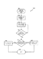
図1は、集積回路(IC)を調査する方法の一実施形態を示すフローチャート100である。ブロック101において、調査に用いるICを準備する。裸のダイ(die)の状態で調査を行うことができるように、前記ICのダイをパッケージから取り出す必要がある。ブロック102において、コンタクトエッチストップ層(CESL)の上部にある材料又は層(複数)の少なくとも少量を除去する。或る場合には、これにより、プリメタル絶縁(PMD)層が露出され得る。ウェットエッチング、ドライエッチング、化学機械研磨(CMP、chemical mechanical planarization)、化学研磨、又は機械研磨などの手法は、従来技術として知られており、CESL上部の材料を除去するのに有用である。
FIG. 1 is a
或る集積回路は、当該集積回路の各メタル層内のメタルライン(metal line)にアルミニウムが用いられ、多結晶シリコン層上に形成されたコンポーネント(複数)とこれらメタルラインとを相互接続するビア(via)(複数)にタングステンが用いられて構成される。アルミニウムとタングステンとは選択的にエッチングすることができるので、選択エッチングの手法によりビアをメタルラインから分離して集積回路を分解することができる。メタルラインからビアを識別するには、ビアとメタルラインとの間でコントラストを示す画像を取得することが有用である。タングステンとアルミニウムとは、走査型電子顕微鏡の画像において容易に区別することができる。 In some integrated circuits, aluminum is used for the metal lines in each metal layer of the integrated circuit, and the vias interconnecting the metal lines with the components formed on the polycrystalline silicon layer. Tungsten is used for (via) (plural). Since aluminum and tungsten can be selectively etched, the integrated circuit can be decomposed by separating the via from the metal line by a selective etching method. In order to identify a via from a metal line, it is useful to acquire an image showing contrast between the via and the metal line. Tungsten and aluminum can be easily distinguished in a scanning electron microscope image.
従って、PMD上の材料を除去する一つの方法は、集積回路ダイの、分解された注目エリアのタイルイメージを取得することである。各メタル層は、従来技術において周知の適切な材料を用いた層間絶縁膜(ILD、interlayer dielectric)により覆われている場合がある。メタル層N+1は、従来技術において周知の適切な材料で形成されたバリア層により、その上部に堆積された内部絶縁膜と分離され得る。バリア層は、堆積されたメタル層N+1、Nが、それらの上部に堆積された内部絶縁膜にマイグレート(migrate)するのを防止する。メタル層N+1のメタルラインは、従来技術において周知の方法で形成されたビアにより、メタル層Nのメタルラインに接続され得る。ビアをメタル層Nから分離するバリア層は、導電性であり、そのビアとメタルラインとを電気的に接続する。 Thus, one way to remove material on the PMD is to obtain a disassembled area of interest tile image of the integrated circuit die. Each metal layer may be covered with an interlayer dielectric (ILD) using an appropriate material known in the prior art. The metal layer N + 1 can be separated from the internal insulating film deposited thereon by a barrier layer formed of an appropriate material known in the prior art. The barrier layer prevents the deposited metal layers N + 1, N from migrating to the internal insulating film deposited thereon. The metal line of the metal layer N + 1 can be connected to the metal line of the metal layer N by a via formed by a well-known method in the prior art. The barrier layer that separates the via from the metal layer N is electrically conductive and electrically connects the via and the metal line.
集積回路のタイル画像を取得するには、パッシベーション層と、オプションである何等かのバリア材料とを、まず、ウェットエッチング若しくはドライエッチング、又は化学的研磨及び若しくは機械的研磨の手法により除去して、メタル層N+1のメタルラインを露出させる。次に、その集積回路ダイを、例えば走査型電子顕微鏡などの画像装置の精密ステージ上に配し、従来技術における周知の方法により、注目エリアのタイル画像を取得する。メタル層N+1のタイル画像を取得したら、メタル層N+1を、例えばウェットエッチング若しくはドライエッチング、又は化学的研磨及び若しくは機械的研磨の手法により、除去することができる。このプロセスは、ビアを無傷な状態に維持しつつメタル層N+1を除去するように制御される。その後、ビアを無傷のまま残しつつバリア層と内部絶縁膜とを除去するエッチング溶液が選択される。このエッチングが注意深く制御されていれば、エッチングの終了時には、ビアは無傷のまま残り、ビアによりシールドされ当該ビアを取り巻いているバリア層の部分が除去される。これにより、メタル層Nのメタルラインとビアとが露出し、露出されたビアとメタル層Nのタイル画像が、従来技術における周知の方法で取得される。 To obtain a tile image of an integrated circuit, the passivation layer and any optional barrier material are first removed by wet or dry etching, or chemical and / or mechanical polishing techniques, The metal line of the metal layer N + 1 is exposed. Next, the integrated circuit die is placed on a precision stage of an image device such as a scanning electron microscope, and a tile image of the area of interest is obtained by a known method in the prior art. Once the tile image of the metal layer N + 1 is acquired, the metal layer N + 1 can be removed by, for example, wet etching or dry etching, or chemical and / or mechanical polishing techniques. This process is controlled to remove the metal layer N + 1 while keeping the via intact. Thereafter, an etching solution is selected that removes the barrier layer and the internal insulating film while leaving the via intact. If this etch is carefully controlled, the via remains intact at the end of the etch, and the portion of the barrier layer that is shielded by the via and surrounding the via is removed. As a result, the metal lines and vias of the metal layer N are exposed, and tile images of the exposed vias and the metal layer N are acquired by a known method in the prior art.
このプロセスは、「ボトムアップ」プロセスと称することができる。ビア(複数)が、それらの下端(bottom end)において接続されているメタル層と共に画像化されるためである。この手法は、アルミニウムのメタルラインとタングステンのビアとを用いて構成された集積回路に対しては、これら2つの金属についての異なるエッチング特性を用いるため有効に働くが、最近では、集積回路は銅のメタルラインと銅のビアを用いて製造される。当業者により理解され得るように、ビアとメタルラインとが同じ金属でできている場合には、エッチングプロセスを制御することは困難である。 This process can be referred to as a “bottom-up” process. This is because the vias are imaged with the metal layer connected at their bottom end. This approach works well for integrated circuits constructed with aluminum metal lines and tungsten vias because of the different etch characteristics for these two metals, but recently integrated circuits have been Of metal lines and copper vias. As can be appreciated by those skilled in the art, it is difficult to control the etching process if the via and the metal line are made of the same metal.
集積回路ダイをパッケージングから取り出した後で、第1のメタル層(メタル層N+1)を覆っているパッシベーション層を除去する。パッシベーション層は、従来技術における周知のエッチングプロセスを用いて除去することができる。次に、その下にあるバリア層を露出させるため、当該集積回路はウェットエッチング又はドライエッチングのプロセスにかけられ、メタルラインとビアとがエッチング除去される。メタルラインとビアとをエッチング除去したら、当該チップは精密ステージに配され、注目エリアのタイル画像が取得される。次に、その集積回路に他のメタル層が存在するか否かが判断される。存在する場合には、そのメタルラインを覆っている層間絶縁膜(ILD)と何等かのバリア材料(不図示)も除去される。当業者により理解されるように、バリア層は、通常、メタルラインの下に用いられ、メタルラインの上には用いられない。とはいえ、パッシベーション層又はILDを除去するのに用いられるプロセスは、メタルラインとその下にあるバリア層とを残しつつ、メタルラインを覆うバリア材料も除去するものとすることができる。すべてのメタル層が露出され、エッチング除去され、その画像が取得された後には、プリメタル絶縁膜が残る。 After removing the integrated circuit die from the packaging, the passivation layer covering the first metal layer (metal layer N + 1) is removed. The passivation layer can be removed using well known etching processes in the prior art. Next, in order to expose the underlying barrier layer, the integrated circuit is subjected to a wet or dry etching process, and the metal lines and vias are etched away. When the metal lines and vias are removed by etching, the chip is placed on a precision stage, and a tile image of the area of interest is acquired. Next, it is determined whether another metal layer exists in the integrated circuit. If present, the interlayer dielectric (ILD) covering the metal line and any barrier material (not shown) are also removed. As will be appreciated by those skilled in the art, the barrier layer is typically used under the metal line and not over the metal line. Nonetheless, the process used to remove the passivation layer or ILD can also remove the barrier material that covers the metal line while leaving the metal line and the underlying barrier layer. After all the metal layer is exposed, etched away, and the image is acquired, the premetal insulating film remains.
銅ダマシンプロセス(copper damascene process)を用いて作製された集積回路は、メタル層N+1のメタルラインを覆うパッシベーション膜を備え得る。そのメタルラインは、一のビアにより、メタル層N内のメタルラインと接続される。そのメタルラインは、一のバリア層により層間絶縁材料から分離される。 An integrated circuit fabricated using a copper damascene process may include a passivation film that covers the metal lines of the metal layer N + 1. The metal line is connected to the metal line in the metal layer N by one via. The metal line is separated from the interlayer insulating material by one barrier layer.
バリア層は、導電性を有するものとすることができ、ビアとメタル層Nのメタルラインとの間を接続する。バリア層は、メタルラインを内部絶縁膜から分離し、金属が内部絶縁膜にマイグレートしないようにして、その特性が変化するのを防止する。次に、ウェットエッチング又はドライエッチングのプロセスを用いて、バリア層を残しつつ、メタルラインとビアとを除去する。当業者により理解されるように、この方法は、従来技術に用いられる方法とは逆に、ビア(複数)がそれらの上端(top end)において接続しているメタルラインと共に表示される画像を生成することができる。したがって、このプロセスは、「トップダウン」プロセスと表現することができる。 The barrier layer may be conductive and connects between the via and the metal line of the metal layer N. The barrier layer separates the metal line from the internal insulating film, prevents the metal from migrating to the internal insulating film, and prevents its characteristics from changing. Next, the metal lines and vias are removed using a wet etching process or a dry etching process while leaving the barrier layer. As will be appreciated by those skilled in the art, this method, contrary to the method used in the prior art, produces an image that is displayed with the metal lines connecting vias at their top ends. can do. This process can thus be described as a “top-down” process.
PMDの上にある材料などの、コンタクトエッチストップ層(CESL)の上にある材料の少なくとも少量を除去したら、ブロック103において、そのダイをエッチングし、CESLの上に残っている付加的な材料とCESLの少なくとも少量を除去する。先進のCMOS ICのデバイス構造に関する詳細な解析を用いることにより、コンタクトエッチストップ層(CESL)が、n−FETデバイスとp−FETデバイスとで異なる特性を持ち得ることが発見された。これら2つの異なるCESLではエッチングが異なる速度で発生し、これによりデバイスのタイプを特定することが可能であることが見出された。この特性は、種々の先進CMOSプロセスに関して確認されており、非導電層上に形成された半導体や標準のCMOSプロセスを用いて形成されたデバイス及び又はバルクシリコン基板上に形成されたデバイスを用いるプロセスにおいて見られるような、埋め込み酸化物層(buried-oxide layer)上に構成されたデバイスにおいても現れ得る。
Once at least a small amount of the material above the contact etch stop layer (CESL), such as the material above the PMD, has been removed, the block is etched at
ICをエッチングする方法は、従来技術において周知であり、ドライエッチング又はウェットエッチングを含む。いくつかの実施形態では、フレオンや六フッ化硫黄などの種々の高エネルギーガスを用いる反応性イオンエッチング(RIE、reactive-ion etching)などのドライエッチングを用いるものとすることができる。他のいくつかの実施形態では、酸又はその他の液体を用いるウェットエッチングを用いるものとすることができる。一の実施形態では、水、フッ化水素酸、及び酢酸の混合液を、ウェットエッチング剤として用いるものとすることができる。いくつかの実施形態では、エッチングは、予め定められた所定の時間期間だけ続けられる。いくつかの実施形態では、この所定の時間期間は、30秒と60秒との間であるが、他の実施形態では、この所定の時間期間は、これよりも短いか又は長いものとすることができる。いくつかの実施形態では、エッチング時間は、エッチングプロセスからのフィードバックを用いて制御されるものとすることができる。 Methods for etching ICs are well known in the prior art and include dry or wet etching. In some embodiments, dry etching such as reactive ion etching (RIE) using various high energy gases such as freon and sulfur hexafluoride may be used. In some other embodiments, wet etching using acids or other liquids may be used. In one embodiment, a mixture of water, hydrofluoric acid, and acetic acid can be used as a wet etchant. In some embodiments, the etching is continued for a predetermined predetermined time period. In some embodiments, this predetermined time period is between 30 and 60 seconds, but in other embodiments, this predetermined time period may be shorter or longer. Can do. In some embodiments, the etching time can be controlled using feedback from the etching process.
いくつかの実施形態では、調査対象であるICと同様の作製プロセスを用いて作製されたICを切断し調査して、エッチング時間及び又は上記所定の時間期間の決定に役立てるものとすることができる。断面を調査し、PMD及び又はCESLの厚さを測定及び又は解析して、使用されている材料を特定することができる。PMD及び又はCESLの厚さは、PMD及び又はCESLに含まれる材料や使用するエッチング手法と共に、エッチング時間及び又は上記所定の時間期間を算出するのに有用である。 In some embodiments, an IC fabricated using a fabrication process similar to the IC under investigation can be cut and examined to help determine the etching time and / or the predetermined time period. . Cross-sections can be examined and PMD and / or CESL thicknesses can be measured and / or analyzed to identify the materials being used. The thickness of PMD and / or CESL is useful for calculating the etching time and / or the predetermined time period as well as the material contained in PMD and / or CESL and the etching technique used.
ブロック104において、ICが精査され、p−FETを覆うCESLの領域が、n−FETを覆うCESLの領域に対し差異を生じているか否かが観察される。いくつかの実施形態では、エッチングプロセスの後で、IC上面の顕微鏡写真を作成するため、走査型電子顕微鏡を用いることが必要となり得る。他のいくつかの実施形態では、光学顕微鏡、原子間力顕微鏡、又はその他の、ICを精査するための方法を用いて、これらのCESLが差異を生じているか否かが観察される。多くのICでは、p−FETを覆うCESLは、n−FETを覆うCESLと異なっており、エッチングが異なる速度で進む等、異なる態様でエッチングが発生し得る。CESLは異なる態様でエッチングされるので、CESLにおけるこの相違に注目し、これを用いて、p−FETを覆うCESLの領域とn−FETを覆うCESLの領域とを区別することができる。いくつかの場合には、2つのタイプのFETを簡単に区別できる程度に、一のタイプのFETの上ではCESLの全部又はほとんど全部が除去され、一方、他のタイプのFETの上ではCESLの有意な量が残存し得る。他のいくつかの場合には、残っているCESLの量の違いはさほど大きくはないが、それでも当業者にとっては顕著ものとなり得る(本開示と、これに関連する請求項(複数)においては、CESLの量とは、CESLの総量ではなく、CESLの厚さ、又は単位面積当たりのCESLの量を意味し得る)。他のいくつかの場合には、2つのタイプのFETを覆うCESLの、不透明度、色、表面状態(texture)、物理的高さ、又はその他同様の特性などの、他の特性が異なるものとなり得る。
At
n−FETデバイスを覆うCESLの領域とp−FETデバイスを覆うCESLの領域とが、ブロック104における初期エッチングの後において差異を生じていない場合には、ブロック103においてエッチングステップがもう一度実行されるものとすることができる。このステップは、n−FETデバイスを覆うCESLの領域とp−FETデバイスを覆うCESLの領域とが差異を生ずるまで、繰り返されるものとすることができる。後続のエッチングステップは、同じ所定の時間長さだけ行われるものしてもよいし、当該所定の時間長さよりも短いか、又は長いものとすることもできる。一の実施形態では、後続のエッチングステップの長さは、オーバエッチングの発生可能性を最小限にし、かつ、n-FETデバイス及びp-FETデバイスの両方からCESLを完全に除去されてしまう可能性を最小化すべく、上記所定の時間長さよりも短いものとすることができる。他の実施形態では、オペレータは、顕微鏡写真を用いて、後続エッチングステップの時間長さの決定に役立てることができる。
If the region of CESL covering the n-FET device and the region of CESL covering the p-FET device has not made a difference after the initial etching in
n−FETデバイスを覆うCESLの領域とp−FETデバイスを覆うCESLの領域とに差異を生ずるような適切な量のエッチングが完了すると、ブロック105において、特定のデバイスフットプリント(占有領域、footprint)又はフットプリントの集合を分析して、CESLの量がより多いか又はより少ないかを観察する。他の実施形態では、他の特性を用いてCESLの領域を区別するものとすることができる。特定のデバイスフットプリント又はフットプリントの集合に、より多い量のCESLが存在する場合には、ブロック106において、そのデバイスをp−FETデバイスとして特定することができる。特定のデバイスフットプリント又はフットプリントの集合が、より少ない量のCESLを有する場合には、ブロック107において、そのデバイスをn−FETデバイスとして特定することができる。他のいくつかの実施形態においては、p−FETデバイスを覆うCESLは、そのCESLの特性と使用するエッチングプロセスに応じて、より速くエッチングされ得る。それらの実施形態では、p−FETデバイスは、より少ない量のCESLを持つことによって特定することができ、n−FETデバイスは、より多い量のCESLを持つことによって特定することができる。注目しているデバイスフットプリントが特定された後、ブロック108において本プロセスは終了する。ここに説明する方法は、広汎な種類のICに関して有用であり、以下に説明する例に限定されるものではない。
When an appropriate amount of etching has been completed to make a difference between the region of CESL covering the n-FET device and the region of CESL covering the p-FET device, at block 105 a specific device footprint (occupied region, footprint) is obtained. Alternatively, the footprint set is analyzed to observe whether the amount of CESL is greater or less. In other embodiments, other characteristics may be used to distinguish CESL regions. If there is a greater amount of CESL in a particular device footprint or set of footprints, at
図2Aは、相補型金属酸化物半導体(CMOS)IC260の断面の概念図である。シリコンウェハからダイに切り出された基板201は、その上面に非導電層202を有する。非導電層202の上には、p−FET220とn−FET230とが形成されている。
FIG. 2A is a conceptual diagram of a cross section of a complementary metal oxide semiconductor (CMOS)
コンタクトエッチストップ層(CESL)は、ICの少なくとも能動領域(active area)の上部に堆積されている。p−FET用に設計された第1のタイプのCESL層229は、p−FET220等のp−FETが形成された領域の上に堆積される。n−FET用に設計された第2のタイプのCESL層239は、n−FET230等のn−FETが形成された領域の上に堆積される。第1のタイプのCESLは、第2のタイプのCESLとは異なる特性を持ち得る。種々のICプロセスについての、これら2つのタイプのCESLの相違のいくつかは、それらの厚さの相違、材料の相違、イオン注入量の相違、多層か単層か、又はその他の相違を含み得る。CESLの上のポリシリコンの層は、相互配線用に用いることができるが、図2Aには示されていない。CESLの上には、プリメタル絶縁(PMD)層203が堆積されている。
A contact etch stop layer (CESL) is deposited over at least the active area of the IC. A first type of
メタル配線の一つ又は複数の層が、PMDの上に堆積され得る。メタルの第1の層205は、相互配線間に設けられた絶縁層204と共に堆積されている。第1メタル層205と絶縁層204の上には、絶縁層206と共にメタルの第2の層207が堆積されている。メタルの第2の層207と絶縁層206の上には、絶縁層208と共にメタルの第3の層209が堆積されている。ビアを用いて層間を接続することができる。
One or more layers of metal wiring may be deposited on the PMD. The
図2Bは、プリメタル絶縁(PMD)層203まで層(複数)が除去されたCMOS IC260の断面の概念図である。この図は、フローチャート100のブロック102の処理が実行された後の、IC260の状態に相当する。メタル相互配線層205、207、209と絶縁層204、206、208が除去されていることに注意されたい。PMD層203の上方にある材料は、ウェットエッチング、ドライエッチング、CMP、又はその他の研磨技術などの、種々の手法を用いて除去することができる。第1及び第2のタイプのCESL229、239と、n−FET230及びp−FET220は、本処理プロセスのこのステップにおいては何の影響も受けない。
FIG. 2B is a conceptual diagram of a cross-section of the
図2Cは、CESL229、239の少量がエッチング除去された後の、CMOS IC260の断面の概念図である。この図は、フローチャート100のブロック103/104の処理が実行された後の、IC260の状態に相当する。図2Cにおいて、第2のタイプのCESL239が完全に除去されている点に注意されたい。第1のタイプのCESL229は、部分的にエッチング除去され、図2Cにおいては図2Bよりも薄くなっている。いくつかの実施形態においては、第2のタイプのCESL239の全てが除去されるのではなく、第2のタイプのCESLの薄い層が残るものとすることができる。p−FET220がn−FET230と区別できる限りにおいて、第2のタイプのCESL239を全て除去することは重要ではない。
FIG. 2C is a conceptual diagram of a cross-section of
図2Cには、これらのFETの詳細が示されている。p−FET220は、pタイプのソース222とドレイン223とを備えた本体部221を有している。薄いゲート酸化膜224により、ポリシリコンゲート225が本体部221から分離されている。本体部221は、nタイプ材料がドープされた又はドープされていない、シリコン又はその他の半導体材料で構成することができる。ゲート225に、ソース222及び又はドレイン223に対する負電圧が印加されると、本体部221内にpチャネルが形成される。n−FET230は、nタイプのソース232とドレイン233とを備えた本体部231を有している。薄いゲート酸化膜234により、ポリシリコンゲート235が本体部231から分離されている。本体部231は、pタイプ材料がドープされた又はドープされていない、シリコン又はその他の半導体材料で構成することができる。ゲート235に、ソース232及び又はドレイン233に対する正電圧が印加されると、本体部231内にnチャネルが形成される。
FIG. 2C shows details of these FETs. The p-
図2Dは、図2Cと同様にCESL229、239の少量がエッチング除去された後の、CMOS IC260の平面視の概念図であり、p−FET220及びn−FET230のフットプリントを示している。図2A、2B、及び2Cに示した断面図は、切断ライン200で示した位置における断面図である。p−FET220及びn−FET230の双方と共に、非導電層202が見えている。この例では、第2のタイプのCESL239は、全て除去されているため見ることはできない。ビア接続部238を有するゲート235、ビア接続部236を有するソース232、及びビア接続部237を有するドレイン233を含む、n−FET230のフットプリントの種々の部分が見えている。第1のタイプのCESL229は、部分的にエッチング除去され、未だ見える状態となっている。ビア接続部228を有するゲート225、ビア接続部226を有するソース222、及びビア接続部237を有するドレイン223を含む、p−FET220のフットプリントの種々の部分が、第1のタイプのCESL229を介して見えている。n−FET230及びp−FET220の見えている部分を、フットプリントと称することができる。図2Dに示すフットプリント(複数)は単純化されているが、実際のデバイスのフットプリントは、従来技術において良く知られており、当業者により認識され得る。
FIG. 2D is a plan view conceptual diagram of the
第2のタイプのCESL239に比べて第1のタイプのCESL229の量が多いと、IC260の特定の領域に存在するデバイスのタイプを特定する際に便利である。ICの上面画像又は平面像を用いることで、断面又はその他のタイプの画像から得られるよりもずっと多くのデバイスを、一枚の画像から特定することができる。上述した種々の実施形態を用いることにより、ICの広い範囲の領域に存在するデバイス(複数)のタイプを、一枚の画像から特定することができる。
A greater amount of the
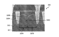
図3A及び図3Bは、CMOS IC300の2つの異なる断面の顕微鏡写真である。図3Aは、IC300の、2つのp−FETデバイス320A及び320Bの部分の断面である。非導電層302の上に形成されたp−FET320A/Bと共に、シリコン基板301と非導電層302が見えている。p−FET320A/Bの上の第1のタイプのCESLは、かすかに見える分離線329Cにより区分された2つの個別の領域329Aと329Bを有している。図3Bは、IC300の、2つのn−FETデバイス330A及び330Bの部分の断面である。非導電層302の上に形成されたn−FET330A/Bと共に、シリコン基板301と非導電層302が見えている。n−FET330A/Bの上の第2のタイプのCESL339は、単なる単一の層であり、p−FET320A/B上の第1のタイプのCESL329よりもずっと薄い。
3A and 3B are photomicrographs of two different cross sections of the
第1のタイプのCESL329と第2のタイプのCESL339とを、他の特性を用いて区別することもできる。ここに示す例では、第1のタイプのCESL329は、周囲の構造と共に、より窪んだメニスカス(meniscus)を持ち、一方、第2のタイプのCESL339は、周囲構造と共に凸状のメニスカスを持つ。他のICでは、第1のタイプのCESLは、当該CESLが覆う領域上に圧縮力を働かせ、第2のタイプのCESLは張力を働かせる。これらの力の効果は、種々の顕微鏡写真で見ることができる。他のICでは、一のタイプのCESLにおいて注入されたイオンを見ることができ、他のタイプのCESLでは見ることができないという場合もある。注入されたイオンは、顕微鏡写真では白い点として見ることができる。従来技術における種々の手法を用いて、CESLに用いられている材料を特定することができる。2つの異なるCESLにおける相違は、何であれ、これらを区別するのに有用である。
The first type CESL 329 and the
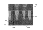
図3Cは、ウェットエッチプロセスを用いてCESLの少量をエッチング除去した後の、CMOS IC300の平面視の顕微鏡写真である。その細部は、種々のデバイスのフットプリントと相互配線である。CESLが残存しているか又は除去されたより広いエリアを認識することができる。図3Dは、図3Cの平面視の概念図であり、CESLエリアの概略を示している。エリア351、エリア353、エリア355、及びエリア357は、残存しているCESLを示している。これらのエリア内に見られるMOSFETは、p−FETデバイスとして特定することができる。エリア352、エリア354、及びエリア356は、CESLのほとんど又は全てがエッチング除去された領域である。これらの領域内のいずれかに形成されたMOSFETは、n−FETデバイスとして特定することができる。
FIG. 3C is a plan view micrograph of the
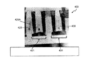
図4Aは、図3に示すIC300とは異なるプロセスを用いて作製された異なるタイプのCMOS IC400の断面の顕微鏡写真である。p−FETデバイス421が、第1のタイプのCESL429に覆われている。第1のタイプのCESL429は、p−FET421上部のより高いドーム構造から判るように圧縮性(compressive)である。IC400における第1のタイプのCESL429の他の特徴は、第1のタイプのCESL429と第2のタイプのCESL439との境界におけるCESLテール(すそ引き)429Aである。n−FETデバイス431は、第2のタイプのCESL439に覆われている。第2のタイプのCESL439は、n−FET431が広幅化(broadening)していることから判るように伸長性(tensile)である。
FIG. 4A is a photomicrograph of a cross-section of a different type of
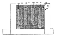
図4Bは、異なるタイプのCMOS IC400の平面視の顕微鏡写真である。この顕微鏡写真は、ウェットエッチプロセスを用いてCESLの少量をエッチング除去した後に撮影されたものである。その細部は、種々のデバイスのフットプリントと相互配線である。或るエリアは、他のエリアよりもCESLが多く残存している。エリア451、エリア453、エリア455、及びエリア457等の、CESLがより多く残存しているエリア内に見られるMOSFETは、p−FETデバイスとして特定することができる。エリア452、エリア454、エリア456、及びエリア458等の、CESLの残存がより少ないエリア内に見られるMOSFETは、n−FETデバイスとして特定することができる。
FIG. 4B is a photomicrograph in plan view of different types of
図5は、ドライエッチプロセスを用いてCESLの少なくとも少量が除去された他のCMOS IC500の、平面視の顕微鏡写真である。CESLの少なくとも少量を反応性イオンエッチングにより除去したものであり、いくつかのエリアは、他のエリアよりもCESLの量が多いことが判る。エリア551及びエリア555等の、CESLがより多く残存しているエリア内に見られるMOSFET(複数)は、p−FETデバイスとして特定することができる。エリア552及びエリア554等の、残属するCESLがより少ないエリア内に見られるMOSFET(複数)は、n−FETデバイスとして特定することができる。
FIG. 5 is a plan view micrograph of another
MOFET(複数)のタイプが特定された後は、その情報と、種々のメタル相互配線層の画像から抽出された情報とを関連付けることが有用である。これを行うには、種々の画像を関連付けて位置合わせし、そのICのネットリストを特定することが有用である。それらの画像は、MOSFETのタイプの特定に用いられるものと同じICダイから取得された画像、又はこれと同じタイプの他のICダイから得られた画像とすることができる。 After the types of MOFETs are identified, it is useful to correlate that information with information extracted from various metal interconnect layer images. To do this, it is useful to associate and align the various images and identify the IC's netlist. The images can be images taken from the same IC die used to identify the type of MOSFET, or images taken from other IC dies of the same type.
一の方法は、N個のメタル層Mを有する集積回路の注目エリアに関するタイル画像(複数)の位置合わせ可能にする。ここで、Nは、1より大きい整数である。この方法は、メタル層(MN)の注目エリアとメタル層(MN−1)の上面の少なくとも一部の画像とが取得できるように、集積回路の表面を調える第1のステップを含む。この方法は、さらに、その集積回路のメタル層(MN)及びメタル層(MN−1)の露出部分の、注目エリアについての少なくとも一つのタイル画像を取得することを含む。そして、メタル層(MN−1)の露出部分についての副タイル画像から、当該メタル層(MN−1)の同じ領域を撮影した主タイル画像に写っているエッジ(複数)と一致するようなエッジ(複数)を抽出する。次に、それぞれのメタル層のタイル画像(複数)に見えるエッジ(複数)のパラメトリック表現を生成する。パラメトリック表現は、抽出された各エッジに関連するメタル層の表示(indication)を含む。このパラメトリック表現を用いて、タイル画像(複数)を垂直方向(vertically)に位置合わせし、当該タイル画像(複数)をデザイン分析ワークステーションに表示させたときに、最も都合のよい状態となるようにする。本発明に従う方法及びシステムを用いることにより、位置合わせを非常に高水準な精度で実現することができる。この位置合わせの精度により、集積回路の注目エリアについての、より正確かつ信頼度の高い分析が可能となる。 One method allows alignment of tile images for an area of interest of an integrated circuit having N metal layers M. Here, N is an integer greater than 1. This method, as the image of at least a portion of the upper surface of the target area and the metal layer of the metal layer (M N) (M N- 1) can be obtained, including a first step of raise money the surface of the integrated circuit. The method further includes obtaining at least one tile image for the area of interest of the exposed portion of the metal layer (M N ) and metal layer (M N-1 ) of the integrated circuit. Then, from sub-tile image for the exposed portions of the metal layer (M N-1), so as to match with the metal layer (M N-1) is reflected in the main tile images obtained by photographing the same area are the edge (s) Simple edges (s) are extracted. Next, a parametric representation of the edge (s) visible in the tile image (s) of each metal layer is generated. The parametric representation includes an indication of the metal layer associated with each extracted edge. Using this parametric representation, the tile image (s) are aligned vertically and the tile image (s) are displayed in the design analysis workstation so that they are in the most convenient state. To do. By using the method and system according to the invention, alignment can be realized with a very high level of accuracy. This alignment accuracy enables a more accurate and reliable analysis of the area of interest of the integrated circuit.
集積回路ダイは、まず精査され、コンポーネントのサイズが特定される。コンポーネントのサイズが可視光領域の範囲であれば、光学顕微鏡を用いて注目エリアの画像が取得される。この場合、従来技術において周知の適切な手法を用いて、注目エリアを露出させる。次に、ステージ上にダイが配され、注目エリアの画像が取得される。第1の画像は、露出したメタル層の画像を取得するための第1の焦点設定で取得される。従来技術において周知のように、層1と層2の間の絶縁層は、一般に透明な誘電体層である。したがって、ステージを動かすことなく光学顕微鏡の焦点を変更することで、露出していない層についての第2の画像を取得することができる。後述するように、第2の画像は、同じステージ位置における露出していない層の、遮られていない部分を表すものである。第1の画像と第2の画像を取得する間においてステージは移動しないため、第1と第2の画像における垂直方向(vertical)の位置関係は正確に保たれる。 The integrated circuit die is first scrutinized to determine the component size. If the size of the component is in the visible light range, an image of the area of interest is acquired using an optical microscope. In this case, the attention area is exposed using an appropriate method known in the prior art. Next, a die is arranged on the stage, and an image of the attention area is acquired. The first image is acquired with a first focus setting for acquiring an image of the exposed metal layer. As is well known in the prior art, the insulating layer between layers 1 and 2 is generally a transparent dielectric layer. Therefore, the second image of the unexposed layer can be acquired by changing the focus of the optical microscope without moving the stage. As will be described later, the second image represents an unobstructed portion of the unexposed layer at the same stage position. Since the stage does not move during the acquisition of the first image and the second image, the vertical positional relationship between the first and second images is accurately maintained.
第1及び第2の画像を取得したら、各画像上の焦点の合っているエッジ(複数)のパラメトリック表現を、各エッジのX座標及びY座標の少なくとも一つを抽出することにより生成する。当業者により理解されるように、タイル画像から抽出された各エッジについてX座標とY座標の両方を定めることはできない。例えば、タイル画像を横切って延在する配線(複数)は、X座標又はY座標の一方のみを提供する。ではあるものの、各エッジは、そのエッジに関連するX座標及びY座標の一方又は両方により抽出されるものとされる。パラメトリック表現は、そのエッジに関連するメタル層の表示も含む。次に、注目エリアの全体について画像が取得されたか否かを判断する。全体について取得されていないときは、本プロセスを繰り返して、注目エリアの他の部分の画像を取得する。注目エリアの全体について画像を取得しているときは、注目している各層の画像が取得されたか否かを判断する。各層の画像が取得されていなときは、新しい層を露出させて、画像取得を開始する。そうでないときは、本プロセスを終了する。 Once the first and second images are acquired, a parametric representation of the in-focus edges on each image is generated by extracting at least one of the X and Y coordinates of each edge. As will be appreciated by those skilled in the art, it is not possible to define both X and Y coordinates for each edge extracted from a tile image. For example, the wiring (s) extending across the tile image provides only one of the X coordinate or the Y coordinate. However, each edge is assumed to be extracted by one or both of the X and Y coordinates associated with that edge. The parametric representation also includes a representation of the metal layer associated with that edge. Next, it is determined whether an image has been acquired for the entire attention area. When the entire image has not been acquired, this process is repeated to acquire an image of another part of the attention area. When images have been acquired for the entire area of interest, it is determined whether images of each layer of interest have been acquired. When the image of each layer is not acquired, a new layer is exposed and image acquisition is started. Otherwise, the process ends.
ダイのコンポーネントサイズが可視光領域の範囲より小さいと判断されると、注目エリアの一の層について、制御されたエッチングプロセスを用いて当該層の全体と当該層の直下にある層の少なくとも一部とを露出させることにより、撮影のための準備が行われる。異方性エッチングを用いることにより良好な結果が得られる場合もある。次に、ダイは、画像取得のため精密ステージ上に配され、そのダイの露出した第1のメタル層と部分的に露出した第2のメタル層の画像が、例えば走査型電子顕微鏡を用いて取得される。走査型電子顕微鏡は、露出した第1のメタル層と少なくとも部分的に露出した第2のメタル層を同時に画像化するのに十分な被写界深度を有している。その後、露出した第1のメタル層と部分的に露出した第2のメタル層のエッジ(複数)のパラメトリック表現が抽出される。抽出されたエッジは、その画像における明度に基づき、第1のメタル層又は第2のメタル層についてのパラメトリック表現に割り当てられる。これは、後述するように、走査型電子顕微鏡が露出した第1のメタル層と部分的に露出した第2のメタル層の両方を写す一枚の画像を取得するのに十分な被写界深度を有しているとはいっても、露出した第1のメタル層は、当該画像においては部分的に露出した第2のメタル層よりも明るく撮影されるためである。 When it is determined that the component size of the die is smaller than the visible light range, using a controlled etching process for one layer of the area of interest, the entire layer and at least a portion of the layer immediately below the layer Are prepared for shooting. Good results may be obtained by using anisotropic etching. Next, the die is placed on a precision stage for image acquisition, and an image of the exposed first metal layer and the partially exposed second metal layer is obtained using, for example, a scanning electron microscope. To be acquired. The scanning electron microscope has a depth of field sufficient to simultaneously image the exposed first metal layer and the at least partially exposed second metal layer. Thereafter, parametric representations of the edge (s) of the exposed first metal layer and the partially exposed second metal layer are extracted. The extracted edges are assigned to parametric representations for the first metal layer or the second metal layer based on the lightness in the image. As will be described later, this is a depth of field sufficient to acquire a single image that captures both the first metal layer exposed by the scanning electron microscope and the second metal layer partially exposed. This is because the exposed first metal layer is photographed brighter than the partially exposed second metal layer in the image.
次に、注目エリアの全体を画像化したか否かが判断される。全体が画像化されていないときは、ダイは、従来技術において周知の方法によりステージ位置を調整することにより再配置され、更なる画像が取得される。注目エリアの全体が画像化されたときは、注目している各層が画像化されたか否かが判断される。各層が画像化されていないときは、本プロセスはもとに戻り、ICの層の他のセットを除去して、注目している層の撮影準備が行われる。当業者により理解されるように、第1及び第2の層の画像取得を行った後に、従来技術において周知の方法により、バッフィング又はポリッシングを用いてダイサンプルから第1の層が除去される。さらに理解されるように、他の方法として、異なるダイを用いて、各層の画像取得準備を行うものとすることもできる。 Next, it is determined whether or not the entire attention area has been imaged. When the whole is not imaged, the die is repositioned by adjusting the stage position by methods well known in the prior art, and additional images are acquired. When the entire area of interest has been imaged, it is determined whether or not each layer of interest has been imaged. If each layer is not imaged, the process returns to the other set of IC layers to remove the other set of ICs and prepare the layer of interest for imaging. As will be appreciated by those skilled in the art, after image acquisition of the first and second layers, the first layer is removed from the die sample using buffing or polishing by methods well known in the art. As will be further understood, other methods may be used to prepare the image acquisition for each layer using different dies.
メタル層Nのタイル画像が生成される。これらは、メタル層N上の集積回路コンポーネント(複数)のみを表示するように焦点合わせされた画像(複数)である。これらの画像は、従来技術において周知の方法により、組み合わされて一枚のモザイク画像となる。光学顕微鏡から得られたこれらのタイル画像は、メタル層Nの主画像(一つのメタル層のみを示すように焦点合わせされた画像)である。当業者により理解されるように、集積回路のメタル層(複数)は、可視光に対して透明なシリコンガラス層により分離されている。しかしながら、必要な倍率のため、一の画像取得処理の実行時に光学顕微鏡上の焦点位置に配することができるのは一の層のみである。メタル層MN−1の副画像(焦点位置において部分的に遮られた層を表している)が取得される。 A tile image of the metal layer N is generated. These are the image (s) focused to display only the integrated circuit component (s) on the metal layer N. These images are combined into a single mosaic image by a method well known in the prior art. These tile images obtained from the optical microscope are main images of the metal layer N (images focused so as to show only one metal layer). As will be appreciated by those skilled in the art, the metal layers of the integrated circuit are separated by a silicon glass layer that is transparent to visible light. However, because of the required magnification, only one layer can be placed at the focal position on the optical microscope during execution of one image acquisition process. A sub-image of the metal layer MN-1 (representing a partially blocked layer at the focal position) is acquired.
当業者により良く理解されるように、走査型電子顕微鏡は光学顕微鏡よりも被写界深度が深い。したがって、露出した2つの層を同時に取得することができ、走査型電子顕微鏡の画像パラメータの選択には依存するものの、一の層は他の層よりもエッジが明るく撮影される。これを行うため、上述のように、集積回路を、管理されたプロセスによりエッチングして、メタル層MNを露出させると共に、メタル層MN−1を部分的に露出させる。当業者により理解されるように、2つのメタル層を分離している誘電体層は、走査型電子顕微鏡に対しては不透明である。モザイクのように分割された画像についての視覚分析を容易にするには、各メタル層について、当該メタル層のみが露出している画像をそれぞれ取得することが望ましい。これらのモザイク状のタイル画像の目合わせ(位置合わせ、alignment)は、後述するように主画像と副画像を用いることにより、正確に行うことができる。 As is well understood by those skilled in the art, a scanning electron microscope has a greater depth of field than an optical microscope. Therefore, two exposed layers can be acquired simultaneously, and one layer is photographed with a brighter edge than the other layer, depending on the selection of the image parameter of the scanning electron microscope. To do this, as described above, the integrated circuit is etched by controlled process, to expose the metal layer M N, to expose the metal layer M N-1 partially. As will be appreciated by those skilled in the art, the dielectric layer separating the two metal layers is opaque to a scanning electron microscope. In order to facilitate visual analysis of an image divided like a mosaic, it is desirable to acquire, for each metal layer, an image in which only the metal layer is exposed. The alignment (alignment) of these mosaic tile images can be accurately performed by using a main image and a sub-image as will be described later.
タイル画像のパラメトリック表現を調整して当該タイル画像間の疑似的な目合わせを行うアルゴリズムが有用である。当業者により理解されるように、集積回路の基部層(bottom layer)は、通常、多結晶シリコン層であり、この層の上に集積回路コンポーネント(複数)が構築される。その上の層(複数)は、第1層のコンポーネント(複数)を相互接続するワイヤ及び又はバスを含むメタル相互配線層(複数)である。したがって、注目エリアを分析する目的で画像モザイクを構成する際には、通常は最も底部の層をレイヤ1とし、ダイ座標空間基準(すなわち、その上の各層の方位決定に用いられる座標空間)として用いる。したがって、アルゴリズムは、多結晶シリコン層をメタル層Nとし、画像が通常取得される順序とは逆の順で画像モザイクの目合わせが実行されるものとして動作する。 An algorithm that adjusts the parametric representation of tile images and performs artificial alignment between the tile images is useful. As will be appreciated by those skilled in the art, the bottom layer of an integrated circuit is typically a polycrystalline silicon layer upon which integrated circuit components are built. The layer (s) above it is a metal interconnect layer (s) that includes wires and / or buses interconnecting the first layer components (s). Therefore, when constructing an image mosaic for the purpose of analyzing the area of interest, usually the lowest layer is layer 1 and the die coordinate space reference (ie, the coordinate space used to determine the orientation of each layer above it) Use. Therefore, the algorithm operates on the assumption that the polycrystalline silicon layer is the metal layer N, and image mosaic alignment is executed in the reverse order to the order in which images are normally acquired.
本アルゴリズムは、メタル層N+1の副タイル画像のパラメトリック表現をメタル層N+1の主タイル画像のパラメトリック表現と比較して、共通のエッジを特定することから始まる。共通のエッジが何も特定されない場合、メタル層N+1のパラメトリック表現は内挿用にフラッグが立てられ、その画像モザイクにおける次のタイル画像のパラメトリック表現が選択される。共通エッジが存在すると判断されると、層N+1の主タイル画像表現が、層N+1の副タイル画像のパラメトリック表現に対して位置調整される。上述したように、層N+1の副タイル画像は、対応する層Nのタイル画像と完全に一致することが判っている。N+1主タイル画像とN+1副タイル画像との間の目合わせは、これら2つのパラメトリック表現における共通エッジのX座標とY座標とを調整して、N+1主タイル画像がN+1副タイル画像に一致するようにすることで行われる。次に、層N+1の主タイル画像のパラメトリック表現における他のエッジ座標を、同じX、Yオフセットを用いて位置調整する。次に、その画像モザイクに他のタイル画像が存在するか否かを判断する。存在するときは、主タイル画像と副タイル画像のパラメトリック表現が選択される。 The algorithm begins by comparing the parametric representation of the subtile image of the metal layer N + 1 with the parametric representation of the main tile image of the metal layer N + 1 to identify common edges. If no common edge is identified, the parametric representation of the metal layer N + 1 is flagged for interpolation and the parametric representation of the next tile image in the image mosaic is selected. If it is determined that a common edge is present, the primary tile image representation of layer N + 1 is aligned with the parametric representation of the subtile image of layer N + 1. As described above, it has been found that the subtile image of layer N + 1 completely matches the corresponding tile image of layer N. The alignment between the N + 1 main tile image and the N + 1 subtile image is performed by adjusting the X and Y coordinates of the common edge in these two parametric representations so that the N + 1 main tile image matches the N + 1 subtile image. It is done by. Next, the other edge coordinates in the parametric representation of the main tile image of layer N + 1 are adjusted using the same X and Y offsets. Next, it is determined whether another tile image exists in the image mosaic. If present, a parametric representation of the main tile image and the subtile image is selected.
層N+1の画像モザイクに他のタイル画像が残っていないときは、内挿用のフラグが立てられたパラメトリック表現が存在するか否かを判断する。存在しないときは、同じ集積回路ダイの他の層の画像が存在するか否かを判断する。存在しないときは、本プロセスは終了する。存在するときは、Nを1だけインクリメントし、サンプルダイの次のタイル画像モザイクを処理すべく、本処理が繰り返される。 When no other tile image remains in the image mosaic of the layer N + 1, it is determined whether or not there is a parametric expression that is flagged for interpolation. If not, it is determined whether there are images of other layers of the same integrated circuit die. If not, the process ends. If present, N is incremented by 1 and the process is repeated to process the next tile image mosaic of the sample die.
内挿用にフラグが立てられたパラメトリック表現が存在すると判断されたときは、それらのフラグが立てられたパラメトリック表現の最初の一つが選択される。必要な座標を有する少なくとも3つの隣接するタイル画像のパラメトリック表現を用いて、未知のX座標及び又はY座標が内挿される。次に、フラグが立てられた主タイル画像のパラメトリック表現が、内挿されたデータを用いて更新される。この詳細については後述する。次に、層N+1の主タイル画像のパラメトリック表現におけるエッジ座標が、その前に算出したX、Y座標オフセットを用いて調整される。次に、フラグが立てられた他のパラメトリック表現があるか否かが判断される。 When it is determined that there are parametric expressions flagged for interpolation, the first one of the flagged parametric expressions is selected. The unknown X and / or Y coordinates are interpolated using a parametric representation of at least three adjacent tile images with the required coordinates. Next, the parametric representation of the flagged main tile image is updated with the interpolated data. Details of this will be described later. Next, the edge coordinates in the parametric representation of the main tile image of layer N + 1 are adjusted using the previously calculated X and Y coordinate offsets. Next, it is determined whether there are other parametric expressions flagged.
集積回路ダイの注目エリアの主タイル画像と副タイル画像の両方に共通エッジが存在しない場合が起こり得る。当業者により理解されるように、このような状況は、例えば、注目エリアの主タイル画像が、対応する副タイル画像においては上部の層構造により遮られて見えなくなっている一つ又は複数の特徴物のみを含んでいる場合に発生し得る。 There may be a case where there is no common edge in both the main tile image and the sub tile image in the area of interest of the integrated circuit die. As will be appreciated by those skilled in the art, such a situation is, for example, one or more features in which the main tile image of the area of interest is obstructed by the upper layer structure in the corresponding sub-tile image. It can occur when it contains only things.
メタル層Nと遮られているメタル層N−1とを含む副画像は、視認可能なビアを含んでいる。このビアは、メタル層Nの画像モザイクにおいてはメタル層Nの平行なワイヤにより遮られている場合もあるが、メタル層N−1のモザイク画像上では視認可能であり得る。位置合わせ用データは、メタル層N−1の主画像のパラメトリック表現から抽出される。当業者により理解されるように、隣接するいくつかの点のうちの少なくとも一つの座標が既知である場合において一の点の座標を見出すための、多くの方法が知られている。例を挙げると、これを行う一つの方法は、ドロネー三角形分割(Delaunay triangulation)と称される既知の手法を用いることである。 The sub-image including the metal layer N and the shielded metal layer N-1 includes a visible via. This via may be blocked by parallel wires of the metal layer N in the image mosaic of the metal layer N, but may be visible on the mosaic image of the metal layer N-1. The alignment data is extracted from the parametric representation of the main image of the metal layer N-1. As will be appreciated by those skilled in the art, many methods are known for finding the coordinates of a point when the coordinates of at least one of several adjacent points are known. By way of example, one way to do this is to use a known technique called Delaunay triangulation.
ビアのXオフセットは、ドロネー三角形分割を用いて3つの既知の点の間の値を内挿することにより行うことができる。3つの既知のX座標(例えば既知のXオフセットが与えられた画像モザイク内の位置)が存在するときは、ビアの位置は、これら既知の点間の三角形(単数)をより小さな3つの三角形に分割する。次に、より小さな三角形のそれぞれの面積が算出される。ドロネー三角形分割を知る当業者により理解されるように、これらの三角形の各面積と元の三角形の面積との比は、その三角形の反対側(opposite side)に対する重みを与える。当業者によりさらに理解されるように、ドロネー三角形分割を用いるべくアルゴリズムを最適化することが可能である。同様の処理を繰り返して、メタル層N−1の主画像に見えるビアのYオフセットデータを算出する。 Via X-offset can be done by interpolating values between three known points using Delaunay triangulation. When there are three known X-coordinates (eg, a position in the image mosaic given a known X-offset), the via position will change the triangle (s) between these known points to three smaller triangles. To divide. Next, the area of each smaller triangle is calculated. As will be appreciated by those skilled in the art of Delaunay triangulation, the ratio of the area of each of these triangles to the area of the original triangle gives a weight to the opposite side of the triangle. As will be further understood by those skilled in the art, it is possible to optimize the algorithm to use Delaunay triangulation. Similar processing is repeated to calculate the Y offset data of the via visible in the main image of the metal layer N-1.
集積回路ダイの注目エリアのスライス(断片、slice)を表すタイル画像(複数)を表示するための処理を用いることができる。当業者により理解されるように、注目エリアの「スライス」とは、後述するように、デザイン分析ワークステーションを用いて注目エリアを分析する技術アナリスト(engineer analysts)により指定されるエリアである。 A process for displaying the tile image (s) representing slices (slices) of the area of interest of the integrated circuit die can be used. As will be appreciated by those skilled in the art, a “slice” of an area of interest is an area specified by an engineer analysts who analyze the area of interest using a design analysis workstation, as described below.
デザイン分析ワークステーションは、例えば当該デザイン分析ワークステーションに接続されたマウスを用いる技術アナリストからスライスの座標を受信すると、スライスを構成するのに必要な層Nの画像を画像記憶部から引き出して、層Nのスライスを組み立てる(アセンブル(assemble)する)。次に、システムは、層Nをダイ座標空間基準として指定して、そのスライスにおける他の全ての層の位置調整に用いるダイ座標空間を提供する。当業者により理解されるように、モザイク画像の実際の目合わせ(位置調整)は、デザイン分析ワークステーションにより「オン・ザ・フライ(on-the-fly)」で実行される。これは、アルゴリズムが満足な結果をもたらさず、技術アナリスト(複数)の経験や判断から正しく表示されていないタイル画像間の正しい位置合わせを行うべきと考えられる領域があるときに、当該技術アナリストによって位置調整のオフセットを追加又は変更することができるようにすることで行われる。画像取得プロセスの出力は、上述したように、それら画像間の位置調整オフセットを付加した画像モザイクの集合であり、当業者により理解されるように、完全に目合わせがされた画像モザイクの集合ではない。技術アナリストは、主画像及び副画像と、自身の経験とを用いて、上述したアルゴリズムが発生させた位置調整エラーを修正することができる。 For example, when the design analysis workstation receives the coordinates of the slice from a technical analyst using a mouse connected to the design analysis workstation, the design analysis workstation extracts an image of the layer N necessary to configure the slice from the image storage unit, Assemble layer N slices (assemble). The system then designates layer N as the die coordinate space reference and provides a die coordinate space that is used to align all other layers in the slice. As will be appreciated by those skilled in the art, the actual alignment (alignment) of the mosaic image is performed “on-the-fly” by the design analysis workstation. This can be done when there is an area where the algorithm does not give a satisfactory result and there is a region where it is thought that correct alignment between tile images that are not displayed correctly should be made based on the experience and judgment of the technical analyst. This is done by allowing the list to add or change the offset of the alignment. The output of the image acquisition process is, as described above, a set of image mosaics with an alignment offset between the images, as will be understood by those skilled in the art, Absent. A technical analyst can use the main and sub-images and his own experience to correct the alignment error generated by the algorithm described above.
システムは、スライス座標に関連する層N+1のタイル画像を画像記憶部から取り出して、層N+1のスライスを組み立てる。次に、層N+1のスライスは、上述のように算出されたパラメトリック表現を用いて、層Nのスライス座標空間基準に対して位置調整される。次に、集積回路ダイの他の層があるか否かを判断する。他の層があるときは、Nを1だけインクリメントして、本プロセスを繰り返す。他の層がないときは、そのスライスが、デザイン分析ワークステーションの画面上の指定された数のウィンドウ内に表示される。 The system retrieves the layer N + 1 tile image associated with the slice coordinates from the image store and assembles the slice of layer N + 1. Next, the slice of layer N + 1 is aligned with respect to the slice coordinate space reference of layer N using the parametric representation calculated as described above. Next, it is determined whether there are other layers of the integrated circuit die. If there are other layers, increment N by 1 and repeat the process. When there are no other layers, the slice is displayed in a specified number of windows on the design analysis workstation screen.
技術アナリストが入力を行ったか否かが判断される。技術アナリストが終了コマンドを入力したときは、本プロセスは終了する。技術アナリストがスクロール、パン(pan)、ズーム等のコマンドを入力したときは、本プロセスが部分的に繰り返される。ただし、技術アナリストがスライス層モザイクのいずれかにおけるいずれかのタイル画像について、新たな座標調整を入力すると、システムは、選択された層Yにおける選択されたタイル画像についての新しい座標オフセットを受け付け、そのタイル画像のパラメトリック表現を調整する。次に、システムは、層Yのスライスモザイクを、層Y−1のスライスモザイクに対して再び位置調整し、その後、上記アナリスト入力の結果として得られたパラメトリック表現データを用いて、層Y+1、...、Nのそれぞれが、そのスライスの層Yに対して再び位置調整される。 It is determined whether a technical analyst has made an input. The process ends when the technical analyst enters a termination command. When a technical analyst enters commands such as scroll, pan, zoom, etc., the process is partially repeated. However, if a technical analyst enters a new coordinate adjustment for any tile image in any of the slice layer mosaics, the system accepts a new coordinate offset for the selected tile image in the selected layer Y, Adjust the parametric representation of the tile image. Next, the system re-aligns the slice mosaic of layer Y with respect to the slice mosaic of layer Y-1, and then uses the parametric representation data obtained as a result of the analyst input to create layer Y + 1, . . . , N are again aligned with respect to layer Y of the slice.
他のプロセスを用いて、集積回路ダイの注目エリアの3次元モデルを算出することができる。本アルゴリズムは、モデリングプログラムからスライス座標を受信することで開始する。注目エリアについて選択された所望の一部がモデル化される場合であっても、スライス座標はその注目エリア全体の座標である。スライス座標を受信すると、アルゴリズムは、画像記憶部から層Nの画像を取り出して、層Nのスライスに関するパラメトリックデータを組み立てる(アセンブル(assemble)する)。次に、システムは、層Nをダイ座標空間基準として指定する。任意選択として、アルゴリズムは、層Nのタイル画像を分析し、従来技術における周知の方法によりパターンマッチングを用いてネットリストを構築することができる。次に、システムは、スライス座標に関連する層N+1のタイル画像を画像記憶部から取り出して、層N+1のスライスデータを組み立てる。次に、システムは、パラメトリック表現データを用いて、層N+1のスライスデータを層Nのスライスデータに対して位置合わせする。次に、画像記憶部に他の層の画像があるか否かを判断する。他の層の画像があるときは、Nを1だけインクリメントし、本プロセスが部分的に繰り返される。他の層がないときは、垂直方向(vertically)に位置合わせされたスライスデータがモデリングプログラムへ渡され、モデリングプログラムが実行されて、従来技術における周知の方法により、そのスライスの3次元モデルが構築される。次に、アルゴリズムは、モデリングプログラムからのフィードバックを待機する。フィードバックは、終了プログラムコマンドとすることができ、この場合には、本アルゴリズムは終了する。モデリングプログラムは、データ内の矛盾を検出し、座標調整値(coordinate adjustment)をアルゴリズムに送って画像目合わせにエラーがあることを示すことができる。アルゴリズムは、モデリングプログラムから座標調整値を受け取ると、層Yにおける選択されたタイル画像のパラメトリック表現を調整する。次に、アルゴリズムは、層Yのスライスを層Y−1のスライスに対して再度位置合わせ(realign)し、次に、パラメトリック表現データを用いて、再位置合わせされたそのスライスの層Yに対して層Y+1、...Nを位置合わせする。その後に、アルゴリズムは、垂直方向(vertically)に再位置合わせされたスライスデータをモデリングプログラムに渡す。 Other processes can be used to calculate a three-dimensional model of the area of interest of the integrated circuit die. The algorithm starts by receiving slice coordinates from a modeling program. Even when the desired part selected for the area of interest is modeled, the slice coordinates are the coordinates of the entire area of interest. Upon receipt of the slice coordinates, the algorithm retrieves the layer N image from the image storage and assembles (assembles) the parametric data for the layer N slice. Next, the system designates layer N as the die coordinate space reference. Optionally, the algorithm can analyze the layer N tile images and build a netlist using pattern matching by methods well known in the art. The system then retrieves the layer N + 1 tile image associated with the slice coordinates from the image store and assembles the slice data for layer N + 1. The system then aligns layer N + 1 slice data with layer N slice data using parametric representation data. Next, it is determined whether there is an image of another layer in the image storage unit. If there are other layer images, N is incremented by 1 and the process is partially repeated. When there are no other layers, the vertically aligned slice data is passed to the modeling program and the modeling program is executed to build a three-dimensional model of the slice by well-known methods in the prior art. Is done. The algorithm then waits for feedback from the modeling program. The feedback can be an exit program command, in which case the algorithm ends. The modeling program can detect inconsistencies in the data and send coordinate adjustments to the algorithm to indicate that there is an error in image alignment. When the algorithm receives coordinate adjustment values from the modeling program, it adjusts the parametric representation of the selected tile image in layer Y. The algorithm then realigns the slice in layer Y with respect to the slice in layer Y-1, and then uses the parametric representation data to realign the layer Y in that slice. Layers Y + 1,. . . Align N. Thereafter, the algorithm passes the vertically realigned slice data to the modeling program.
集積回路のリバースエンジニアリングでは、通常、ウェハ、切断済みのダイ、又はこれらの部分をマイクロイメージングシステム(micro-imaging system)を用いて調査して、設計検証や競争力分析のための、設計情報及びレイアウト情報を引き出す処理が行われる。マイクロイメージングシステムには、高倍率光学顕微鏡、走査型電子顕微鏡、電界放射型電子顕微鏡(field emission electron microscope)等が含まれる。試料であるダイの高倍率のタイル画像は、コンピュータワークステーションの管理の下に、各分解ステップの間に取得される。コンピュータワークステーションは、制御信号を用いてマイクロイメージングシステムを制御する。コンピュータワークステーションは、マイクロイメージングシステムから画像データを受信し、そのタイル画像データを、ハードディスク等のメモリ、通常は大容量記憶装置に保存する。一般に、タイル画像データは、大容量記憶装置に送られ、コンピュータワークステーションと大容量記憶装置との間のデータ通信要件を最小化し、かつ大容量記憶装置でのデータ記憶要件を最小化するように、圧縮形式で保存される。 In reverse engineering of integrated circuits, the design information and design analysis and competitiveness analysis are usually performed by examining the wafer, cut dies, or parts thereof using a micro-imaging system. A process for extracting layout information is performed. The micro imaging system includes a high magnification optical microscope, a scanning electron microscope, a field emission electron microscope, and the like. A high-magnification tile image of the sample die is acquired during each decomposition step under the control of a computer workstation. The computer workstation controls the micro-imaging system using control signals. The computer workstation receives image data from the micro-imaging system and stores the tile image data in a memory such as a hard disk, usually a mass storage device. In general, tile image data is sent to a mass storage device to minimize data communication requirements between the computer workstation and the mass storage device and to minimize data storage requirements on the mass storage device. Saved in a compressed format.
保存されたタイル画像は、画像モザイクに組み立てられる。各画像モザイクは、一の分解ステップにおけるダイの注目面を表している。ダイのタイル画像を取得する際には、サンプル座標空間が定義される。サンプル座標空間は、タイル画像及び画像モザイクの位置合わせに用いられる。 The stored tile images are assembled into an image mosaic. Each image mosaic represents the attention surface of the die in one decomposition step. When acquiring a die tile image, a sample coordinate space is defined. The sample coordinate space is used for alignment of tile images and image mosaics.
デザイン分析ワークステーション(DAW、design analysis workstation)は、技術アナリストが、写真、マーカーペン、及び紙を用いる代わりに、ポインティングデバイスと画像モニタを用いてICをリバースエンジニアリングすることを可能にする。デザイン分析ワークステーションは、画像モザイクへの注釈付与(annotating)や設計・レイアウト表示機能により、技術アナリストがチップのリバースエンジニアリングを行えるようにするためのリバースエンジニアリング・システムとして機能する。ICのリバースエンジニアリングにおける「チップ」とは、これを用いて分析対象である集積回路に関するデータを構築するための基本オブジェクト(fundamental object)である。チップは、複数の層を備える。各層は、それぞれ、物理的なIC上の物理的な相互配線層に対応する。一の層は、一又は複数のダイ写真、一又は複数の画像モザイク、及び一又は複数のアノテーションオーバレイのいずれか一つである。 Design analysis workstations (DAWs) allow technical analysts to reverse engineer ICs using pointing devices and image monitors instead of using photos, marker pens, and paper. The design analysis workstation functions as a reverse engineering system that allows technical analysts to reverse engineer chips by annotating image mosaics and design and layout display functions. A “chip” in reverse engineering of an IC is a basic object (fundamental object) for building data related to an integrated circuit to be analyzed using this. The chip comprises a plurality of layers. Each layer corresponds to a physical interconnection layer on a physical IC. One layer is any one of one or more die photographs, one or more image mosaics, and one or more annotation overlays.
上述したように、一の画像モザイクは、取得された複数のタイル画像の一の配列である。タイル画像は、分解を開始する前の集積回路の全体を捉えた画像であるダイ写真よりも高倍率である。タイル画像(複数)は、互いに接するように並べられて、特定の分解ステップの後における集積回路の、大きな、境目のない、高倍率の画像を形成する。各画像モザイクには、一つ又は複数のアノテーションオーバレイを用いて注釈を付すことができる。これについては後述する。 As described above, one image mosaic is an array of a plurality of acquired tile images. The tile image has a higher magnification than a die photograph, which is an image that captures the entire integrated circuit before starting decomposition. The tile images are arranged in contact with each other to form a large, borderless, high magnification image of the integrated circuit after a particular decomposition step. Each image mosaic can be annotated using one or more annotation overlays. This will be described later.
設計情報とレイアウト情報を引き出すための集積回路の分析においては、技術アナリストは、DAWを利用する。DAWは、表示装置と、キーボードと、マウス(これに限定されるものではない)などのポインティングデバイスと、を備える。表示装置は表示エリアを有し、表示エリアは、対応する表示座標空間を規定する。表示エリアに表示されるシステムポインタは、ポインティングデバイスにより制御される。システムポインタは、望ましくは特徴のある形状、サイズ、及び色を有する。 In analyzing an integrated circuit for extracting design information and layout information, a technical analyst uses a DAW. The DAW includes a display device, a keyboard, and a pointing device such as a mouse (not limited to this). The display device has a display area, and the display area defines a corresponding display coordinate space. A system pointer displayed in the display area is controlled by a pointing device. The system pointer desirably has a characteristic shape, size, and color.
表示装置は、通常は陰極線管(CRT、Cathode Ray Tube)、液晶表示装置(LCD、Liquid Crystal Display)、イメージプロジェクタにより投影される画像等である。これに代えて、デザイン分析ワークステーションの表示装置として、マルチディスプレイ(multi-headed visual display)(不図示)により構成される分散表示装置(distributed visual display)や、複数のワークステーションの表示装置を用いた分散ウィンドウイング環境(distributed windowing environment)を含むものとすることができる。分散ウィンドウイング環境は、XConsortium(登録商標)、NeXTStep(登録商標)/OpenStep(登録商標)等から市販されている。 The display device is usually a cathode ray tube (CRT), a liquid crystal display (LCD), an image projected by an image projector, or the like. Instead, as a display device for a design analysis workstation, a distributed display device comprising a multi-headed visual display (not shown) or a display device for a plurality of workstations is used. It may include a distributed windowing environment. Distributed windowing environments are commercially available from XConsortium (registered trademark), NeXTStep (registered trademark) / OpenStep (registered trademark), and the like.
本発明に従い、複数の技術アナリストは、複数のデザイン分析ワークステーションを操作して、共有する画像モザイクから、分解した一つの集積回路を表す設計情報とレイアウト情報とを、同時並行的に抽出することができる。本システムは、一つのICリバースエンジニアリングプロジェクトに携わる複数の技術アナリストの同期作業を容易にするための、マルチユーザ拡張機能を備える。これについては、アノテーションオブジェクトの所有権との関連において以下に詳細に説明する。 According to the present invention, a plurality of technical analysts operate a plurality of design analysis workstations to simultaneously extract design information and layout information representing one disassembled integrated circuit from a shared image mosaic. be able to. The system includes a multi-user extension function to facilitate the synchronization work of a plurality of technical analysts involved in one IC reverse engineering project. This will be described in detail below in relation to ownership of the annotation object.
表示エリアは、ナビゲーションウィンドウとモザイクビュー(複数)とを表示する。モザイクビューは、それぞれビュー境界(view-boundary)を有する。ナビゲーションウィンドウは、分析対象である集積回路の全体像を提供する。ナビゲーションウィンドウは、その集積回路の低解像度のデジタル画像を表示する。分析対象のサンプルが単一のICダイ又はその主要部分である場合、ナビゲーションウィンドウに表示される低解像度画像は、ダイ写真と称される。スライスは、ナビゲーションウィンドウ内で選択され、ダイ写真の注目エリアを規定する。 The display area displays a navigation window and mosaic views (plural). Each mosaic view has a view-boundary. The navigation window provides an overview of the integrated circuit being analyzed. The navigation window displays a low resolution digital image of the integrated circuit. When the sample to be analyzed is a single IC die or a main part thereof, the low resolution image displayed in the navigation window is called a die photograph. The slice is selected in the navigation window and defines the area of interest of the die photo.
スライスは、ポインティングデバイスを用いてナビゲーションウィンドウ内でシステムポインタの位置を定めることにより、ナビゲーションウィンドウ内で生成される。システムポインタの位置をナビゲーションウィンドウ内に持って行くと、システムポインタはマスターカーソルとして再構成されて表示され、技術アナリストによるマウスクリックなどのトリガイベントが有効となる。このトリガイベントにより、ツール選択メニューが起動される。ツール選択メニューは、例えばポップアップメニューである。ツール選択メニューに表示されるメニューアイテムにより、技術アナリストはスライス作成ツールを起動することができる。スライス作成ツールは、ダイ写真上の注目エリアを選択するのに用いられる。この選択は、ポインティングデバイスをクリックして注目エリアの一の頂点を指定し、マスターカーソルを斜めにドラッグして矩形のスライスを作成することにより行われる。ツール選択メニューも、プルダウンメニューとすることができる。スライス作成ツールは、スライス作成手段(slice creator)の一つの形式を表すものである。本発明の代替の実施形態に従うと、スライス作成ツールは、スライス作成コマンドを発行することによって起動するものとすることができる。さらに他の実施形態に従うと、「ホットキー」を用いてスライス作成を起動するものとすることができる。当業者により理解されるように、他の方法を用いてスライス作成を起動するものとすることもできる。 A slice is generated in the navigation window by locating the system pointer in the navigation window using a pointing device. When the position of the system pointer is brought into the navigation window, the system pointer is reconfigured and displayed as a master cursor, and a trigger event such as a mouse click by a technical analyst becomes effective. This trigger event activates the tool selection menu. The tool selection menu is, for example, a pop-up menu. The menu item displayed in the tool selection menu allows the technical analyst to launch the slice creation tool. The slice creation tool is used to select an area of interest on a die photo. This selection is performed by clicking the pointing device to specify one vertex of the area of interest and dragging the master cursor diagonally to create a rectangular slice. The tool selection menu can also be a pull-down menu. The slice creation tool represents one form of slice creator. According to an alternative embodiment of the present invention, the slice creation tool may be activated by issuing a slice creation command. According to yet another embodiment, a “hot key” may be used to activate slice creation. As will be appreciated by those skilled in the art, other methods may be used to trigger slice creation.
このマンマシン・インタフェースは、技術アナリストの操作に応答して生成されるイベントを監視するイベントドリブン・インタフェースである。当業者により理解されるように、インタフェース・イベントは、マンマシン・インタフェースのデザインや技術アナリストの選択に依存して、複数の方法で生成され得る。例えば、上述したように、スライス作成は、ポップアップメニュー、プルダウンメニュー、ホットキー、又はコマンドモードの操作により有効にするものとすることができる。本発明に従い、マンマシン・インタフェースにおいて、これらのオプションのいずれか一つ又は複数を有効にすることができる。 This man-machine interface is an event-driven interface that monitors events generated in response to operations of technical analysts. As will be appreciated by those skilled in the art, interface events can be generated in a number of ways, depending on the design of the man-machine interface and the choice of a technical analyst. For example, as described above, slice creation can be enabled by a pop-up menu, pull-down menu, hot key, or command mode operation. In accordance with the present invention, any one or more of these options can be enabled in the man-machine interface.
イベントは、検出され分析されて、スライス作成についての要求であるか否かが判断される。上述したように、スライス作成は、例えば、メニュー選択、コマンドライン、又はホットキーを用いて起動するものとすることができる。そのイベントがスライス作成要求ではない場合、そのイベントは処理されて、イベントの監視が再開される。そのイベントをスライス開始イベントであると判断した場合、スライス作成プロセスは、ダイ写真上の注目エリアを規定するスライス座標が返されるのを監視する。例えば所定の時間間隔の間に座標が返されると、システムポインタの位置がダイ写真上にあるか否かが判断される。システムポインタがダイ写真上にある場合、プロセスは、元に戻って注目エリアの選択を待機する。システムポインタがダイ写真上にない場合、技術アナリストに対し、ダイ写真上で注目エリアを選択するよう指示するメッセージが表示される。 The event is detected and analyzed to determine if it is a request for slice creation. As described above, slice creation can be initiated using, for example, menu selection, command line, or hot keys. If the event is not a slice creation request, the event is processed and event monitoring is resumed. If the event is determined to be a slice start event, the slice creation process monitors the return of slice coordinates that define the area of interest on the die photo. For example, if coordinates are returned during a predetermined time interval, it is determined whether the position of the system pointer is on the die photograph. If the system pointer is on the die photo, the process goes back and waits for selection of the area of interest. If the system pointer is not on the die photo, a message instructing the technical analyst to select the area of interest on the die photo is displayed.
スライス座標が受信されると、当該スライス座標はメモリに保存され、スライス作成パラメータが調査されて自動モザイクビュー作成が有効であるか否かが判断される。自動モザイクビュー作成は、本発明の望ましい実施形態に従って与えられる機能であり、スライスに関連する各画像モザイクについてモザイクビューを自動的に作成する。代替的に、一のスライスについて表示すべきモザイクビュー(複数)を、そのスライスに関連する全ての画像モザイクのリストから選択するものとすることができる。スライス作成パラメータが、自動モザイクビュー作成が有効であることを示している場合、画像モザイクリストが取り出され、各画像モザイクについて、そのスライス座標により規定される一のモザイクビューが作成されて表示スペースに表示される。 When the slice coordinates are received, the slice coordinates are stored in memory, and the slice creation parameters are examined to determine whether automatic mosaic view creation is enabled. Automatic mosaic view creation is a function provided in accordance with a preferred embodiment of the present invention that automatically creates a mosaic view for each image mosaic associated with a slice. Alternatively, the mosaic view (s) to be displayed for a slice may be selected from a list of all image mosaics associated with that slice. If the slice creation parameter indicates that automatic mosaic view creation is enabled, the image mosaic list is retrieved, and for each image mosaic, one mosaic view defined by its slice coordinates is created and displayed in the display space. Is displayed.
スライス作成パラメータが、自動モザイクビュー作成が起動されていることを示している場合、一の画像モザイクリストが取り出されて、そのスライス座標により規定される一のモザイクビューが各画像モザイクについて作成され、それらのモザイクビューが表示スペースに表示される。 If the slice creation parameter indicates that automatic mosaic view creation is activated, one image mosaic list is retrieved and one mosaic view defined by its slice coordinates is created for each image mosaic, Those mosaic views are displayed in the display space.
自動モザイクビュー作成が有効でないと判断された場合、そのスライスに関連する画像モザイクのリストが表示エリアに表示され、これにより技術アナリストは、モザイクビューを作成すべき画像モザイクを選択することができる。スライス作成プロセスは、表示されたリストから少なくとも一つの画像モザイクが選択されたか否かを判断する。選択されていないときは、画像モザイクを選択するか又はプロセスをキャンセルするよう要求するメッセージを表示する。選択された各画像モザイクについてモザイクビューが作成され、スライス作成プロセスは終了する。 If it is determined that automatic mosaic view creation is not enabled, a list of image mosaics associated with the slice is displayed in the display area, allowing the technical analyst to select the image mosaic for which the mosaic view should be created. . The slice creation process determines whether at least one image mosaic has been selected from the displayed list. If not, display a message requesting to select an image mosaic or cancel the process. A mosaic view is created for each selected image mosaic and the slice creation process ends.
ロックステップ・カーソルの動作(lock-step cursor motion)を制御するプロセスが開始する。このプロセスは、カーソルイベントを検出するカーソルイベント処理ループの一部である。カーソルイベントは分析され、当該カーソルイベントがカーソルの動きを示すものであるか否かが判断される。カーソルの動きを示すものでないときは、そのカーソルイベントが処理される。「終了(exit)ボタンのクリック」のようなカーソルイベントは、本プロセスを終了させる。 The process of controlling the lock-step cursor motion begins. This process is part of a cursor event processing loop that detects cursor events. The cursor event is analyzed to determine whether the cursor event is indicative of cursor movement. If it does not indicate cursor movement, the cursor event is processed. A cursor event such as “click on exit button” terminates the process.
受信したカーソルイベントがカーソルの移動を表すものであると判断された場合、本プロセスは、表示座標に関してシステムポインタが一のモザイクビューのビュー境界を横切ったか否かを判断する。システムポインタがビュー境界を横切ったと判断されたときは、本プロセスは、システムポインタがビューの内部へ向かって横切ったのか、ビューから出て行ったのかを判断する。システムポインタがビュー内部に向かって横切ったと判断された場合、システムポインタは、表示エリア上においてマスターカーソルを表すように描画(paint)される。システムポインタの表示座標は、サンプル座標に変換される。現在登録されている全てのビューのリストが取得され、そのリスト内の全てのビューについて処理が繰り返されて、システムのマスターカーソルのサンプル座標を含むカーソルイベントが、これらのビューのそれぞれに対して送信される。各ビューは、マスターカーソルのサンプル座標を当該ビューの表示座標に変換し、そのビュー内のビュー座標にロックステップ・カーソルを表示する。次に、本プロセスは戻って処理を繰り返す。 If it is determined that the received cursor event represents cursor movement, the process determines whether the system pointer crosses the view boundary of one mosaic view with respect to display coordinates. When it is determined that the system pointer has crossed the view boundary, the process determines whether the system pointer has crossed towards the interior of the view or has left the view. If it is determined that the system pointer has crossed into the view, the system pointer is painted to represent the master cursor on the display area. The display coordinates of the system pointer are converted into sample coordinates. A list of all currently registered views is obtained, the process is repeated for all views in the list, and a cursor event containing the system master cursor sample coordinates is sent to each of these views. Is done. Each view converts sample coordinates of the master cursor into display coordinates of the view, and displays a lockstep cursor at the view coordinates in the view. The process then returns and repeats the process.
システムポインタがビューから出て行ったと判断された場合、システムポインタの外見は、オペレーティングシステム表示に戻される。プロセスは、登録されているビューのリストを取得し、そのリストについて処理を繰り返して、登録されている各ビューにカーソルイベントを送信する。カーソルイベントを受信すると、各ビューはロックステップ・カーソルをそのビューから消去し、本プロセスは戻って処理を繰り返す。 If it is determined that the system pointer has left the view, the appearance of the system pointer is returned to the operating system display. The process obtains a list of registered views, repeats the process for that list, and sends a cursor event to each registered view. When a cursor event is received, each view deletes the lockstep cursor from that view, and the process returns and repeats the process.
カーソルイベントがカーソルの移動を示すものであり、システムポインタがビュー境界を横切っていないと判断された場合、本プロセスは、システムポインタがビュー内にあるか否かを判断する。ビュー内にないときは、本プロセスは戻って処理を繰り返す。 If the cursor event indicates cursor movement and it is determined that the system pointer does not cross the view boundary, the process determines whether the system pointer is in view. If not in view, the process returns and repeats.
システムポインタがビュー内にあるときにカーソル移動イベントが受信された場合、マスターカーソルの表示座標は、サンプル座標に変換される。登録されているビューのリストが取り出され、カーソルイベントと、サンプル座標空間に関するマスターカーソルの新しいポジションとが、登録された各ビューに対して繰り返し処理により送信される。各ビューは、ロックステップ・カーソルを、新しい座標を受信したときに存在していた位置で消去し、マスターカーソルのサンプル座標を、そのビューの表示座標に変換する。次に、そのビューは、その表示座標がそのビュー内であれば、その新しい表示座標にロックステップ・カーソルを再描画する。 If a cursor movement event is received when the system pointer is in view, the display coordinates of the master cursor are converted to sample coordinates. A list of registered views is retrieved, and the cursor event and the new position of the master cursor with respect to the sample coordinate space are sent to each registered view in an iterative process. Each view erases the lockstep cursor at the position that was present when the new coordinates were received, and converts the master cursor sample coordinates to the display coordinates of the view. The view then redraws the lockstep cursor at the new display coordinates if the display coordinates are within the view.
ロックステップ・カーソルの移動は、全てのビューに広がる範囲を持ったグローバルデータ構造(global data structure)を使って有効にすることもできる。グローバルデータ構造は、少なくとも、調査対象である物理的な試料ICにより定義されるサンプル座標空間に関するマスターカーソルの位置を記憶する。マンマシン・インタフェースは、ポインティングデバイスから受信したシステムポインタ・イベントを処理する。各システムポインタ・イベントが、通常はシステム割り込みを介して受信されると、マンマシン・インタフェースは、システムポインタを現在の位置に表示し、マスターカーソルの位置を更新する。システムポインタは、一のビューのビュー境界内にあるときは、マスターカーソルの形状と構成とにより画面上に描画され、サンプル座標空間におけるマスターカーソルの位置が算出されてグローバルデータ構造に記憶される。割り込み処理の一部として、他の各ビューは、サンプル座標空間におけるマスターカーソルの位置を、当該ビューのビュー境界内において表示可能であるか否かを判断する。表示可能であれば、そのビューは、表示されているロックアップ・カーソルのサンプル座標空間位置とグローバルデータ構造内に記憶されている位置とを比較し、必要に応じてそのビュー内でロックステップ・カーソルを消去して再描画する。 Lockstep cursor movement can also be enabled using a global data structure that spans all views. The global data structure stores at least the position of the master cursor with respect to the sample coordinate space defined by the physical specimen IC to be investigated. The man machine interface processes system pointer events received from the pointing device. As each system pointer event is received, typically via a system interrupt, the man-machine interface displays the system pointer at the current position and updates the position of the master cursor. When the system pointer is within the view boundary of one view, the system pointer is drawn on the screen according to the shape and configuration of the master cursor, and the position of the master cursor in the sample coordinate space is calculated and stored in the global data structure. As part of the interrupt process, each of the other views determines whether the position of the master cursor in the sample coordinate space can be displayed within the view boundary of the view. If so, the view compares the sample coordinate space position of the displayed lockup cursor to the position stored in the global data structure and, if necessary, lockstep Erase the cursor and redraw.
それぞれにシステムポインタを持つワークステーションが複数用いられて、一の試料ICを表す複数の画像モザイクから同時並行的に設計情報とレイアウト情報とが抽出される場合、マスターカーソル競合の問題は、システムポインタがマスターカーソルであるか否かを、選択基準を用いて判断することにより解決することができる。選択基準は、特定のワークステーションの特定のシステムポインタに制限すること、カーソルイベントを発生した最後のシステムポインタを選択すること、等を含むものとすることができる。 When multiple workstations each having a system pointer are used and design information and layout information are extracted simultaneously from a plurality of image mosaics representing one sample IC, the problem of master cursor contention is that the system pointer It can be solved by determining whether or not is a master cursor using a selection criterion. Selection criteria may include limiting to a specific system pointer for a specific workstation, selecting the last system pointer that generated a cursor event, and so on.
モザイクビュー(複数)は、ICを分解するプロセスにおける特定の分解ステップの後に取得された一の画像モザイクの部分(複数)を表示する。スライスは、各モザイクビューにおいて表示される注目エリアを規定する。 The mosaic view (s) displays the portion (s) of one image mosaic acquired after a particular decomposition step in the process of decomposing the IC. The slice defines an area of interest displayed in each mosaic view.
ロックステップ・カーソルは、適切なときに各モザイクビュー内に表示される。対応するロックステップ・カーソルが、ナビゲーションウィンドウにも表示される。望ましくは、ロックステップ・カーソル(複数)は、マスターカーソルを除き、似たような形状、サイズ、及び色を持つ。マスターカーソルは、システムポインタがモザイクビュー内にあるときは、ポインティングデバイスにより制御されるシステムポインタの現在位置を示す。マスターカーソルは、システムポインタと同じ外観を持つものとしてもよいし、特徴的な形状、サイズ、及び又は色を持つものとしてもよい。ロックステップ・カーソル(複数)は、マスターカーソルの制御の下に一斉に動く。これらのロックステップ・カーソルは、サンプル座標空間における位置座標を、マスターカーソルと共有しているためである。
ロックステップの動きは、残像効果(trailing effect)として図中に示される。
A lockstep cursor is displayed in each mosaic view when appropriate. A corresponding lockstep cursor is also displayed in the navigation window. Preferably, the lockstep cursor (s) have a similar shape, size and color except for the master cursor. The master cursor indicates the current position of the system pointer controlled by the pointing device when the system pointer is in the mosaic view. The master cursor may have the same appearance as the system pointer, or may have a characteristic shape, size, and / or color. The lockstep cursor (s) move all together under the control of the master cursor. This is because these lockstep cursors share the position coordinates in the sample coordinate space with the master cursor.
The movement of the lockstep is shown in the figure as a trailing effect.
本発明の望ましい実施形態に従うと、モザイクビュー(複数)は、スライスがズーム又はパンされるのに合わせて、一斉にズーム及び又はパンする。これを行うため、ナビゲーションウィンドウは、パンニングスライダ(panning sliders)を備えるように表示される。 According to a preferred embodiment of the present invention, the mosaic view (s) zoom and / or pan all at once as the slice is zoomed or panned. To do this, the navigation window is displayed with panning sliders.
スライスは、関連するモザイクビュー(複数)を持つことができる。モザイクビュー(複数)は、それらのモザイクビューのいずれか一つがズーム又はパンされるのに合わせてズーム又はパンする。これを行うため、各モザイクビューは、パンニングスライダを備える。ナビゲーションウィンドウは、定義された他の一のスライスを持つことができる。スライスは、モザイクビュー(複数)に関連付けられる。モザイクビュー(複数)は異なるサイズを持つことができ、各モザイクビューは、独立にサイズ変更され及びズームされるものとすることができる。 A slice can have associated mosaic views. The mosaic view (s) zoom or pan as any one of those mosaic views is zoomed or panned. To do this, each mosaic view includes a panning slider. The navigation window can have one other slice defined. A slice is associated with the mosaic view (s). The mosaic view (s) can have different sizes, and each mosaic view can be resized and zoomed independently.
モザイクビュー内部のマスターカーソルにより、マウスクリックやキーシーケンスによる起動などのインタラクティブ・イベントが実行される。これに応答して、アノテーションオーバレイ選択メニューが表示される。アノテーションオーバレイ選択メニューは、分析対象であるチップに関するアノテーションオーバレイのリストを提供し、それらのアノテーションオーバレイの一つを選択することができる。示すように、いずれのアノテーションオーバレイも、いずれかの画像モザイク上に表示することができ、アノテーションオーバレイ上でアノテーションオブジェクトを描画することにより、当該表示から設計やレイアウトを抽出することができる。 Interactive events such as mouse clicks and activation by key sequences are executed by the master cursor inside the mosaic view. In response to this, an annotation overlay selection menu is displayed. The annotation overlay selection menu provides a list of annotation overlays related to the chip to be analyzed, and allows one of those annotation overlays to be selected. As shown, any annotation overlay can be displayed on any image mosaic, and by drawing an annotation object on the annotation overlay, a design or layout can be extracted from the display.
アノテーションオブジェクトは、少なくとも一つのモザイクビュー内に表示された少なくとも一つの画像モザイクから推測された特徴物に基づいて、技術アナリストがアノテーションオーバレイ上に描画したエンティティ(entity)である。画像モザイク(複数)は、ソース画像(source image)(複数)である。画像モザイク(単数)は、各モザイクビューの背景を構成する。アノテーションオブジェクトは、例えば、矩形、線分、多角形、楕円、テキストラベル、接続部、及び配線(ワイヤ)を含む。アノテーションは、画像モザイクとは独立にロードし、及び保存することができる。 An annotation object is an entity drawn on an annotation overlay by a technical analyst based on features estimated from at least one image mosaic displayed in at least one mosaic view. The image mosaic (s) are source image (s). The image mosaic (single) constitutes the background of each mosaic view. An annotation object includes, for example, a rectangle, a line segment, a polygon, an ellipse, a text label, a connection unit, and a wiring (wire). Annotations can be loaded and saved independently of the image mosaic.
モザイクビューは、集積回路の分解ステップのうちメタル層の露出を行った分解ステップから得られた画像モザイクについて表示される。メタルトレース(金属部分の形状)は、現在のパン及びズームの設定において観察することができる。アノテーションオブジェクトは、観察されたトレース特徴(形状特徴、features of trace)に基づいて作成される。アノテーションオブジェクトは、作成された後、そのトレースに重ねられる。 The mosaic view is displayed for the image mosaic obtained from the decomposition step in which the metal layer is exposed among the decomposition steps of the integrated circuit. The metal trace (the shape of the metal part) can be observed in the current pan and zoom settings. An annotation object is created based on the observed trace features (shape features). An annotation object is created and then overlaid on its trace.
上述したように、マルチビュー編集のための機能が提供される。編集操作は、一のモザイクビューで開始して続行され、他のモザイクビューで終了させることができる。マルチビュー編集により、集積回路上のバスのような非常に長いアノテーションオブジェクトを、モザイクビューをスクロールすることなく容易に描画することができる。マルチビュー編集では、画像モザイク(複数)が同じ分解ステップに関連付けられている必要はない。 As described above, a function for multi-view editing is provided. The editing operation can start with one mosaic view and continue and end with another mosaic view. With multi-view editing, very long annotation objects such as buses on an integrated circuit can be easily drawn without scrolling the mosaic view. In multi-view editing, the image mosaic (s) need not be associated with the same decomposition step.
モザイクビュー間で実行される編集操作は、次のようなルールに従う:
アノテーションオブジェクトは、編集操作を開始したモザイクビューに表示されているアノテーションオーバレイに関連付けられる;
アノテーションオブジェクトの移動やコピーを行うと、そのアノテーションオブジェクトは、編集操作を終了したモザイクビューに表示されているアノテーションオーバレイに関連付けられる。
Editing operations performed between mosaic views follow the following rules:
An annotation object is associated with the annotation overlay displayed in the mosaic view that initiated the editing operation;
When the annotation object is moved or copied, the annotation object is associated with the annotation overlay displayed in the mosaic view for which the editing operation has been completed.
少なくとも、マスターカーソルに関連付けられているモザイクビューは、共通アノテーションオブジェクトを取り出すためのツールバーを備えることができる。ツールバーにより、技術アナリストは、単純な又は複雑なアノテーションオブジェクト(複数)を取り出すことができる。これらのオブジェクトは、それぞれ、集積回路の一つ又は複数のコンポーネントを表している。モザイクビューは、ツールバーを備える。 At least the mosaic view associated with the master cursor can include a toolbar for retrieving common annotation objects. The toolbar allows technical analysts to retrieve simple or complex annotation objects. Each of these objects represents one or more components of an integrated circuit. The mosaic view includes a toolbar.
アノテーションオブジェクト(複数)は、アノテーションオブジェクトの集合を選択してオペレータを呼び出すことにより、それらを一緒に操作(manipulate)することができる。ツールバーは、選択されたアノテーションオブジェクトに操作(operations)(複数)を実行するためのオペレータ(複数)への選択実行クリックアクセス(select-and-works click access)を含むこともできる。アノテーションオブジェクトに操作を行うためのオペレータは、基本的なもの(primitive)又は複雑なもの(complex)であり得る。複雑なオペレータを定義するための機能も提供される。オペレータを用いて、アノテーションオブジェクトを削除、編集、移動、回転、反転(mirror)、サイズ変更等することができる。望ましくは、操作のアンドゥ(undoing)及びリドゥ(redoing)のための機能も提供される。アノテーションオブジェクトは、不注意に編集が行われるのを防止すべく、その表示を隠すことができる。表示を隠したオブジェクトは、当該オブジェクトを選択してその表示を前景に移動させることができる。アノテーションオブジェクトは、編集されないようにロックすることもできる。ロックされたオブジェクトは、当該オブジェクトを選択してロックを解除し、編集可能にすることができる。 Annotation objects can be manipulated together by selecting a set of annotation objects and calling an operator. The toolbar may also include select-and-works click access to the operator (s) for performing operations (s) on the selected annotation object. An operator for performing an operation on the annotation object may be basic or complex. A function for defining complex operators is also provided. An operator can delete, edit, move, rotate, mirror, resize, etc. annotation objects. Desirably, functions for undoing and redoing operations are also provided. An annotation object can be hidden from view to prevent inadvertent editing. An object whose display is hidden can be selected and moved to the foreground. Annotation objects can also be locked so that they are not edited. A locked object can be made editable by selecting the object and releasing the lock.
操作を容易にするため、アノテーションオブジェクトをグループ化してアノテーションオブジェクト・グループとすることができる。アノテーションオブジェクトは、階層的にグループ化することができる。すなわち、アノテーションオブジェクト・グループは、これを構成する一つ又は複数のアノテーションオブジェクトの要素グループを含むものとすることができる。アノテーションオブジェクト・グループは、いつでも選択してグループ解除(ungroup)することができる。多角形基本図形(polygon primitives)を用いて生成されたアノテーションオブジェクト(複数)は、一つのアノテーションオブジェクト・グループにまとめることができる。アノテーションオブジェクトの、アノテーションオブジェクト・グループへのグループ化により、セル(cell)/コンポーネントの定義と抽出が可能となる。セルとは、一の名前が与えられた一のアノテーションオブジェクト・グループである。通常、セルは、論理ゲート、フリップフロップ等のコンポーネントや小規模回路を表すのに用いられる。 In order to facilitate operation, annotation objects can be grouped into an annotation object group. Annotation objects can be grouped hierarchically. That is, the annotation object group can include an element group of one or more annotation objects constituting the annotation object group. An annotation object group can be selected and ungrouped at any time. Annotation objects (plural) generated using polygon primitives can be combined into one annotation object group. By grouping annotation objects into annotation object groups, cells / components can be defined and extracted. A cell is a single annotation object group given a single name. Usually, a cell is used to represent a component such as a logic gate or a flip-flop or a small circuit.
アノテーションオブジェクト・グループに対応する一のコンポーネント・セルは、トランジスタを表す。セルは、技術アナリストによりプロパティ(properties)が割り当てられる。セルのプロパティは、少なくとも一つのポートの定義を含む。各ポートには、入力シグナリング、出力シグナリング、双方向シグナリング等の信号方向特性が割り当てられる。DAWは、セル・ライブラリを生成する機能も提供する。セル・ライブラリは、ICの分析に用いられるセルのコレクション(collection)である。 One component cell corresponding to the annotation object group represents a transistor. Cells are assigned properties by a technical analyst. The cell properties include the definition of at least one port. Each port is assigned signal direction characteristics such as input signaling, output signaling, and bidirectional signaling. The DAW also provides a function for generating a cell library. A cell library is a collection of cells used for IC analysis.
アノテーションオブジェクトは属性を持つ。各アノテーションオブジェクトは、そのアノテーションオブジェクトに関する情報を示す予め定められた所定の属性を含む。選択された属性は編集することができる。アノテーションオブジェクトの属性は、中空(hollow)/塗りつぶし(filled)、ベタ塗り(solid fill)/点描塗り(stippled fill)、内部色、境界色、境界線幅、テキストラベル角度、文字フォント、文字色等を含む。多角形は、直線若しくはベジェ曲線の集合、又はこれら2つの組み合わせ(複数)とすることができる。 An annotation object has attributes. Each annotation object includes a predetermined attribute indicating information related to the annotation object. The selected attribute can be edited. Attributes of annotation objects include hollow / filled, solid fill / stipled fill, internal color, border color, border width, text label angle, character font, character color, etc. including. The polygon can be a set of straight lines or Bezier curves, or a combination (plurality) of these two.
配線と接続は、層属性(複数)(layer attributes)を持った特殊なアノテーションオブジェクトである。これらの層属性は、相互配線体(複数)(interconnect entities)を表すために用いられる。配線と接続は、特性を運搬(carry)するシグナルも有している。配線アノテーションオブジェクトは、それに関連する層属性を持つ。この層属性は、その配線が配されている集積回路の層を示す。配線アノテーションオブジェクトに関連付けられた層は、その配線アノテーションオブジェクトの生成のための情報を取得した画像モザイクとは異なるものとすることができる。 Wires and connections are special annotation objects with layer attributes. These layer attributes are used to represent interconnect entities. Wiring and connections also have signals that carry properties. The wiring annotation object has a layer attribute related to it. This layer attribute indicates the layer of the integrated circuit in which the wiring is arranged. The layer associated with the wiring annotation object can be different from the image mosaic from which information for generating the wiring annotation object is acquired.
2つの配線アノテーションオブジェクトは、それらのアノテーションオブジェクトがそれぞれメタル層2及びメタル層1に配されていることを示す層属性を持つ。接続アノテーションは、二つ又はそれ以上のコンポーネント間の電気的接続を表す。コンポーネント間の接続は、望ましくは円又は十字(cross)として表される。各接続は、2つの層属性を持つ。接続は、メタル層1とメタル層2に設定された、その接続についての層属性のセットを持つ。 The two wiring annotation objects have layer attributes indicating that the annotation objects are arranged on the metal layer 2 and the metal layer 1, respectively. A connection annotation represents an electrical connection between two or more components. Connections between components are preferably represented as circles or crosses. Each connection has two layer attributes. The connection has a set of layer attributes for the connection set on the metal layer 1 and the metal layer 2.
配線アノテーションオブジェクトについて、配線アノテーションオブジェクト・ラベリングオペレーションが呼び出されると、配線アノテーションオブジェクト・ラベリングプロセスが開始する。選択された配線アノテーションオブジェクトがシグナル・プロパティを持つ場合は、配線ラベルが生成され、その配線アノテーションオブジェクト・ラベリングプロセスは終了する。配線アノテーションオブジェクトがシグナル・プロパティを持たないと判断された場合、デザイン分析ワークステーションは、選択されたアノテーションオブジェクトに接続されているアノテーションオブジェクト及び又はセルの属性を探索して、それぞれのシグナル・プロパティを特定する。曖昧でないシグナル・プロパティを特定できる場合、そのシグナル・プロパティは、接続されている全てのコンポーネントに伝搬され、配線アノテーションオブジェクト・ラベルが作成される。そうでない場合には、技術アナリストは、接続されているコンポーネント(複数)に伝搬させるべきシグナルラベルを入力するよう促される。技術アナリストからのシグナルラベルを指定する入力が受け付けられる。 When a wiring annotation object labeling operation is called for a wiring annotation object, the wiring annotation object labeling process starts. If the selected wiring annotation object has a signal property, a wiring label is generated, and the wiring annotation object labeling process ends. If it is determined that the wiring annotation object does not have a signal property, the design analysis workstation searches the annotation object and / or cell attributes connected to the selected annotation object and sets each signal property. Identify. If an unambiguous signal property can be identified, the signal property is propagated to all connected components and a wiring annotation object label is created. Otherwise, the technical analyst is prompted to enter a signal label to be propagated to the connected component (s). Input specifying a signal label from a technical analyst is accepted.
本発明に係るデザイン分析ワークステーションの他の実施形態は、作成時にアノテーションオブジェクトに自動的にラベリングを行う機能を提供する。ラベルは、例えば数字ラベル又はテキストラベルとすることができる。複数の技術アナリストが複数のデザイン分析ワークステーションを用いて一つのICを同時並行的に分析する本発明の一実施形態では、自動ラベリングの機能が、グローバルに固有なラベリングサフィックスを提供して、ラベリングの競合が起きないことを保証する。 Another embodiment of the design analysis workstation according to the present invention provides the ability to automatically label annotation objects when created. The label can be, for example, a numeric label or a text label. In one embodiment of the present invention in which multiple technical analysts use a plurality of design analysis workstations to analyze an IC concurrently, the automatic labeling feature provides a globally unique labeling suffix, Ensure that no labeling conflicts occur.
デザイン分析ワークステーションは、測定を実行する機能も備える。測定ユーティリティは、コンポーネント間の距離、トレース幅などの、距離計測を実行する機能を備える。多角形コンポーネントにより覆われたエリアを表すエリア計測も取得されるものとすることができる。 The design analysis workstation also has the ability to perform measurements. The measurement utility has a function of performing distance measurement such as a distance between components and a trace width. An area measurement representing the area covered by the polygon component may also be obtained.
アノテーションオブジェクトには、アノテーションオブジェクト・プロパティも関連付けることができる。アノテーションオブジェクト・プロパティを用いて、任意の情報をアノテーションオブジェクトに付加することができる。アノテーションオブジェクト・プロパティは、キー−バリュー・ペア(key-value pair)である。キーとバリューとは、キャラクタの任意のストリングである。各アノテーションオブジェクトは、任意の数の関連するアノテーションオブジェクト・プロパティを持つことができる。 An annotation object / property can also be associated with the annotation object. Arbitrary information can be added to the annotation object using the annotation object property. An annotation object property is a key-value pair. Keys and values are arbitrary strings of characters. Each annotation object can have any number of associated annotation object properties.
アノテーションオブジェクトは、アノテーションオブジェクト・グループにまとめることもできる。アノテーションオブジェクト・グループは、属性とプロパティとを持つことができる。アノテーションオブジェクト・グループの属性とプロパティは、そのアノテーションオブジェクト・グループを構成するアノテーションオブジェクトの選択された属性とプロパティに対するオーバライド効果(overriding effect)を持ち得る。アノテーションオブジェクト・グループは、編集可能な属性を持ち、当該属性により、繰り返し構造、配列化されたコンポーネント、及び配列化されたセルを定義することができる。繰り返し構造の例は、信号バスである。メモリセルは、配列化されたセルの一例である。デザイン分析ワークステーションは、アノテーションオブジェクト及びアノテーションオブジェクト・グループに関連付けられた属性及びプロパティを表示する機能も提供する。 Annotation objects can also be grouped into annotation object groups. An annotation object group can have attributes and properties. The attributes and properties of the annotation object group can have an overriding effect on the selected attributes and properties of the annotation objects that make up the annotation object group. An annotation object group has an editable attribute, and a repeat structure, an arranged component, and an arranged cell can be defined by the attribute. An example of a repeating structure is a signal bus. A memory cell is an example of an arrayed cell. The design analysis workstation also provides the ability to display attributes and properties associated with annotation objects and annotation object groups.
ポップアップウィンドウ(複数)は、それぞれ、アノテーションオブジェクト及びアノテーションオブジェクト・グループに関連する属性及びプロパティの情報を表示する。ポップアップウィンドウは、マウスクリック、キー押下、メニュー選択肢の起動等のインタラクティブ・イベントに応答して、デザイン分析ワークステーションにより表示される。ポップアップウィンドウは、一時的に表示されるものとすることもできるし、又はそのウィンドウを閉じるための技術アナリストによるアクションがあるまで表示が持続するように構成されるものとすることができる。 The pop-up windows (multiple) display attribute and property information related to the annotation object and annotation object group, respectively. Pop-up windows are displayed by the design analysis workstation in response to interactive events such as mouse clicks, key presses, and menu option activations. The pop-up window can be displayed temporarily or can be configured to persist until there is an action by a technical analyst to close the window.
デザイン分析ワークステーションは、アノテーションオブジェクト又はアノテーションオブジェクト・グループに関連付けられている属性及び又はプロパティに関する抽出条件に基づいてアノテーションオブジェクトを選択する機能を、技術アナリストに提供する。抽出条件に基づくアノテーションオブジェクト又はオブジェクト・グループの選択は、任意選択で、再帰探索により行われる。その場合、再帰探索は、アノテーションオブジェクト・グループをアノテーションオブジェクト要素(複数)にまで構造分析する。アノテーションオブジェクト・グループの要素についての再帰探索は、抑制することができる。抽出条件に基づく探索は論理的に結合されるものとすることができ、アノテーションオブジェクトの選択基準はブール論理を用いて処理されるものとすることができる。 The design analysis workstation provides a technical analyst with the ability to select an annotation object based on attributes and / or property extraction criteria associated with the annotation object or annotation object group. Selection of annotation objects or object groups based on extraction conditions is optionally performed by recursive search. In that case, the recursive search analyzes the structure of the annotation object group up to the annotation object element (s). Recursive searches for annotation object group elements can be suppressed. Searches based on extraction conditions can be logically combined, and annotation object selection criteria can be processed using Boolean logic.
デザイン分析ワークステーションは、抽出条件探索を用いて選択されたアノテーションオブジェクトについてパンやズームを行うための機能も提供する。抽出条件探索を用いて選択されたアノテーションオブジェクトに対応するラベルは、探索結果ビューに表示される。パン機能又はズーム機能の起動は、望ましくは、探索結果ビューにリストされたアノテーションオブジェクトをダブルクリックすることにより行われる。 The design analysis workstation also provides functions for panning and zooming the annotation object selected using the extraction condition search. The label corresponding to the annotation object selected using the extraction condition search is displayed in the search result view. The activation of the pan function or the zoom function is preferably performed by double-clicking an annotation object listed in the search result view.
デザイン分析ワークステーションは、アノテーションオブジェクト及びアノテーションオブジェクト・グループの再帰的な編集を可能とする。再帰編集は、編集操作を中断して他の操作を開始又は実行することを含む。例えば、編集操作の際には、モザイクビューがパンされたりズームされたりする。再帰編集からもたらされる利点は、編集操作の途中でアノテーションオブジェクトを永久記憶装置(permanent storage)に保存できることである。望ましくは、再帰編集は、利用可能なリソースの制約の下で、際限なくネストすることができる。 The design analysis workstation allows recursive editing of annotation objects and annotation object groups. Recursive editing includes interrupting an editing operation and starting or executing another operation. For example, in an editing operation, the mosaic view is panned or zoomed. An advantage that comes from recursive editing is that annotation objects can be saved to permanent storage during the editing operation. Desirably, recursive edits can be nested indefinitely under the constraints of available resources.
一のスライスの、酸化物層とポリシリコン層の画像モザイクを結合させた部分から導出される画像モザイク比較ビューが作成される。画像モザイク比較ビューは、注目する二つ又はそれ以上のモザイクビューを選択することにより導出される。デザイン分析ワークステーションは、それぞれのモザイクビューから2つの「スナップショット」を引き出す。これらのスナップショットは、画像モザイク比較の中で結合される。 An image mosaic comparison view is created that is derived from the combined portion of the image mosaic of the oxide and polysilicon layers of a slice. The image mosaic comparison view is derived by selecting two or more mosaic views of interest. The design analysis workstation draws two “snapshots” from each mosaic view. These snapshots are combined in an image mosaic comparison.
無操作結合(NoOp結合)は、選択されたモザイクビュー(複数)の単純な結合である。2つのスナップショットの加算結合(Add結合)は、選択されたモザイクビューのそれぞれのピクセル輝度をピクセル毎に加算する。加算結合は、異なる分解ステップにおいて集積回路の同じ位置について取得された画像モザイク(複数)を重ねる際に用いられる。2つのスナップショットのFirstMinusSecond表示は、第1のスナップショットのピクセル輝度から第2のスナップショットのピクセル輝度をピクセル毎に減算する。画像モザイク比較ビューは、モザイクビュー(複数)のFirstMinusSecond結合である。画像比較モザイクビューから共通構造が減算される。2つのスナップショットのSecondMinusFirst結合は、第2のスナップショットのピクセル輝度から第1のスナップショットのピクセル輝度をピクセル毎に減算する。異なる輝度を持つエリアは、明るい領域又は暗い領域として際立つように表示される。2つのスナップショットにおいて同じようなピクセル値を持つエリアは、画像モザイク比較ビュー内では、くすんだ灰色で表示される。 A no-operation join (NoOp join) is a simple join of selected mosaic views. The addition combination (Add combination) of two snapshots adds the pixel brightness of each selected mosaic view for each pixel. Additive coupling is used in overlaying image mosaics acquired for the same location of the integrated circuit in different decomposition steps. The FirstMinusSecond display of two snapshots subtracts the pixel brightness of the second snapshot from the pixel brightness of the first snapshot for each pixel. The image mosaic comparison view is a FirstMinusSecond combination of mosaic views (plural). The common structure is subtracted from the image comparison mosaic view. The SecondMinusFirst combination of two snapshots subtracts the pixel intensity of the first snapshot from the pixel intensity of the second snapshot for each pixel. Areas having different luminance are displayed prominently as bright areas or dark areas. Areas with similar pixel values in the two snapshots are displayed in dull gray in the image mosaic comparison view.
AbsoluteDifference結合では、ピクセル輝度がピクセル毎に減算されて絶対値が用いられる。その結果、ブライトネスの全範囲をカバーするようにコントラストが誇張される。これにより、例えば相似するエリア(複数)の明るさが暗い場合でも、AbsoluteDifference結合された画像モザイク比較ビューでは相違する部分が明るく表示されるので、似たようなエリア内で微小な相違部分を調査する際に非常に有用である。 In the AbsoluteDifference combination, the pixel luminance is subtracted for each pixel and the absolute value is used. As a result, the contrast is exaggerated to cover the entire range of brightness. As a result, even when the brightness of similar areas (several areas) is dark, for example, the difference parts are displayed bright in the image mosaic comparison view combined with AbsoluteDifference. It is very useful when
Interweave結合は、同じエリアであるが異なる層を表示する画像モザイク(複数)の2つの部分を結合する際に有用である。2つのスナップショットのピクセルが、チェッカーボードパターンで交互に挟み込まれる。Interweave結合は、加算結合と同様の機能を持ち、ピクセル解像度を犠牲にして、ブライトネスと色の忠実性を改善する。 Interweave combining is useful when combining two parts of an image mosaic (s) that display the same area but different layers. Two snapshot pixels are interleaved in a checkerboard pattern. Interweave Combining has the same functionality as Additive Combining and improves brightness and color fidelity at the expense of pixel resolution.
Flip結合も提供される。Flip結合は、二つ又はそれ以上のスナップショットを交互に表示する際に用いられる。スナップショットの交互表示は、相違部分が「動く」特徴部分として際立つように、選択された時間間隔で繰り返すことができる。 Flip coupling is also provided. Flip join is used when two or more snapshots are displayed alternately. The alternate display of snapshots can be repeated at selected time intervals so that the different parts stand out as “moving” features.
集積回路のデザインには反転構造が含まれる。スナップショットの有用な組合せを取得するため、反転機能が提供される。これにより、反転構造(複数)を方位反転させて重ねることができ、相違部分(もしあれば)が容易に観察される。望ましくは、画像処理ウィンドウはロックステップ・カーソルを表示し、望ましくはロックステップ・カーソルの動きは反転動作を考慮する。 Integrated circuit designs include inversion structures. An inversion function is provided to obtain useful combinations of snapshots. This allows the inverted structures (multiple) to be superimposed with their orientation reversed and different parts (if any) are easily observed. Preferably, the image processing window displays a lockstep cursor, and preferably the movement of the lockstep cursor allows for a reversal operation.
上述したように、複数の技術アナリストが協働して、本発明に従うデザイン分析ワークステーションを用いて一つのチップから設計情報やレイアウト情報を抽出することができる。このため、設計及びレイアウトの並行的な抽出作業を支援するための機能が提供される。 As described above, a plurality of technical analysts can work together to extract design information and layout information from a single chip using the design analysis workstation according to the present invention. For this reason, a function for supporting parallel extraction work of design and layout is provided.
設計及びレイアウトの並行抽出作業に資するため、デザイン分析ワークステーションには或る基本機能(複数)が求められる。これらの機能は、アノテーション所有権追跡、固有アノテーションラベル生成、アノテーションロッキング、及びアノテーションマージングを含む。これらの機能は、協働デザイン分析に求められる基本機能のみを示すものである。 In order to contribute to the parallel extraction work of design and layout, the design analysis workstation is required to have a certain basic function (s). These functions include annotation ownership tracking, unique annotation label generation, annotation locking, and annotation merging. These functions show only basic functions required for collaborative design analysis.
アノテーション所有権追跡は、各アノテーションを作成した技術アナリストの個人識別標識(identification)を追跡し、その作成者によるそのアノテーションの修正のみを許可する。固有アノテーションラベル生成は、複数の技術アナリストが一つのプロジェクトについて同時に作業を行う場合にも、生成される各識別標識(identifier)がそのプロジェクトにおいて固有であることを保証する。アノテーションロッキングは、アノテーション作成者がアノテーションオブジェクトをロックすることを可能とする。これにより、そのアノテーションが他人により編集されるのを防止して、不慮の修正が行われるのを防止する。アノテーションマージングは、他の技術アナリストが所有するアノテーションオブジェクトのローディングを可能とする。 Annotation ownership tracking tracks the identification of the technical analyst who created each annotation and only allows the creator to modify the annotation. Unique annotation label generation ensures that each generated identifier is unique in a project, even when multiple technical analysts work on a project simultaneously. Annotation locking allows annotation creators to lock annotation objects. This prevents the annotation from being edited by others and prevents accidental modification. Annotation merging enables loading of annotation objects owned by other technical analysts.
デザイン分析ワークステーションは、配線アノテーションオブジェクト及び又は接続アノテーションオブジェクトにより接続されたコンポーネント間のシグナル情報の伝搬に関する機能も提供する。配線アノテーションオブジェクト及び接続アノテーションオブジェクトは、それぞれ、シグナルキーを持つプロパティを有する。シグナルキーは、これに関連する配線又は接続が運ぶシグナルの名前を示す。シグナル伝搬処理では、一の特定の集積回路に関連付けられた配線アノテーションオブジェクトと接続アノテーションオブジェクトの全ての接続セットが探索される。最初のセットが選択され、一のシグナル・プロパティを持つそのセット内のアノテーションオブジェクト(複数)の位置が特定される。発見された全てのアノテーションオブジェクトのシグナル指定が同じシグナル値を持つときは、そのシグナル値がその接続セット内のすべてのアノテーションオブジェクトへ伝搬される。そのセットは破棄され、処理すべき他のセットが残っているときは、他の一のセットが選択されて処理が再開される。 The design analysis workstation also provides a function related to propagation of signal information between components connected by the wiring annotation object and / or the connection annotation object. Each of the wiring annotation object and the connection annotation object has a property having a signal key. The signal key indicates the name of the signal carried by the associated wiring or connection. In the signal propagation process, all connection sets of a wiring annotation object and a connection annotation object associated with one specific integrated circuit are searched. The first set is selected and the location of the annotation object (s) within that set with one signal property is identified. If the signal specification of all the annotation objects found has the same signal value, the signal value is propagated to all annotation objects in the connection set. The set is discarded and when another set remains to be processed, another set is selected and processing resumes.
アノテーションオブジェクトの接続セットが二つ又はそれ以上の異なるシグナル値を持つ場合は、競合が発生するまでシグナルの伝搬が試みられる。競合には、これを表示するため及び技術アナリストによる更なる調査のためのフラグが立てられる。シグナル競合は、電気的な短絡を表しており、通常はデザイン分析におけるエラーを指摘するものである。 If the annotation object's connection set has two or more different signal values, signal propagation is attempted until a conflict occurs. Conflicts are flagged for display and for further investigation by technical analysts. Signal contention represents an electrical short and usually points to errors in the design analysis.
デザイン分析ワークスステーションは、シグナル競合の閲覧(browsing)と解析のための機能を提供する。この機能は、その内部に少なくとも一つのシグナル競合の位置が表示されるポップアップビューを含む。望ましくは、競合の閲覧と解析のためのナビゲーションボタンが提供される。シグナル競合フラグにはすべて、或るプロパティ(複数)が付される。これらのプロパティには、「短絡(short)」値を持つ「エラー(error)」キーを持ったプロパティが含まれる。競合する各シグナルに関し、「シグナル(signal)」キーと「シグナルラベル(signal label)」値を持つプロパティが作成される。競合するシグナルを示すアノテーションオブジェクトのラベルは、技術アナリストがデザイン分析ワークステーションを用いて指定することもできる。シグナルの伝搬は、別の技術アナリストが作成したロックされたアノテーションオブジェクトにより防止される。そのような場合、望ましくは、シグナル競合にはフラグが立てられるが、シグナル値は伝搬されない。 The Design Analysis workstation provides functions for browsing and analyzing signal conflicts. This feature includes a pop-up view in which at least one signal contention location is displayed. Preferably, navigation buttons are provided for viewing and analyzing conflicts. A certain property (plurality) is attached to all signal conflict flags. These properties include properties with an “error” key that has a “short” value. For each competing signal, a property is created with a “signal” key and a “signal label” value. Annotation object labels that indicate competing signals can also be specified by a technical analyst using a design analysis workstation. Signal propagation is prevented by locked annotation objects created by another technical analyst. In such a case, desirably signal competition is flagged, but no signal value is propagated.
デザイン分析ワークステーションは、相互接続されたアノテーションオブジェクトから設計情報を抽出するための機能も提供する。この設計情報の抽出は、コンポーネントと接続部のネットリストを生成するのに用いられる。ネットリストは、従来技術において周知である。 The design analysis workstation also provides functionality for extracting design information from the interconnected annotation objects. This design information extraction is used to generate a netlist of components and connections. Netlists are well known in the prior art.
ここで用いた用語は、単に特定の実施形態を説明するためのものであって、本発明を限定することを意図したものではない。ここで用いられているように、文脈上そうでないことが明らかである場合を除き、単数形態の表現は、複数である形態をも含むことを意図するものである。さらに、本明細書に用いられている「備える」、「持つ」、「含む」、及び又は「有する」の語は、そこに記載された特徴(features)、完成体(integers)、ステップ、操作(operations)、要素(elements)、及び又はコンポーネントの存在を示すものであるが、一つ又は複数の他の特徴、完成体、ステップ、操作、要素、コンポーネント、及び又はこれらのグループの存在あるいは付加を排除するものではないことが理解されるであろう。 The terminology used herein is for the purpose of describing particular embodiments only and is not intended to be limiting of the invention. As used herein, unless the context clearly indicates otherwise, a singular form is intended to include a plurality of forms as well. Further, as used herein, the terms “comprising”, “having”, “including”, and “having” refer to the features, integers, steps, operations described therein. (Operations), the presence of elements, and / or components, but the presence or addition of one or more other features, completions, steps, operations, elements, components, and / or groups thereof It will be understood that is not excluded.
請求項における対応する構造、材料、行為、及び機能限定又は工程限定の全ての構成要素の等価物は、具体的に記載された他の請求項に記載の構成要素との組み合わせにおいてその機能を実行するための何らかの構造、機能、又は行為を含むことを意図するものである。種々の実施形態の説明は、例示及び説明を目的とするものであり、本発明を網羅的に示したものではなく、又は開示された形態に本発明を限定するもではない。本発明の範囲及び要旨を逸脱しない範囲において多くの改変及び変形が存在することは当業者にとり明らかであろう。ここに含まれる種々の実施形態は、本発明の原理及びその実用的応用を最も良く説明するため、及び、予期される特定の用途に適するように種々の修正を行った種々の実施形態に関し他の当業者が本発明を理解することができるように、選択され及び記載されたものである。 The equivalent structure, material, action, and function or process limitation equivalents in a claim perform their functions in combination with the other recited claims in the specific claim. It is intended to include any structure, function, or act to do so. The description of various embodiments is for purposes of illustration and description, and is not intended to be exhaustive or to limit the invention to the forms disclosed. It will be apparent to those skilled in the art that many modifications and variations can be made without departing from the scope and spirit of the invention. The various embodiments included herein are intended to best illustrate the principles of the invention and its practical application, and relate to various embodiments that have been modified in various ways to suit the particular application envisaged. Have been selected and described so that those skilled in the art may appreciate the invention.
Claims (18)
コンタクトエッチストップ層(CESL)の上の、前記CMOS−ICの材料の少なくとも少量を除去して、当該CMOS−ICの一の領域における前記CESLの少なくとも一部分を露出させるステップと、
前記CMOS−ICの前記領域をエッチングして、当該領域内に前記CESLの少なくとも少量が残存するように前記CESLの前記露出された部分を部分的に除去するステップと、
前記領域内に残存するCESLの状態を精査してCESLの領域を区別するステップと、
CESLの前記区別された領域に基づき、pチャネル金属酸化物半導体デバイス(p−FET)を含むCMOS−ICの第1の領域と、nチャネル金属酸化物半導体デバイス(n−FET)を含むCMOS−ICの第2の領域と、を特定するステップと、
を有する、方法。 A method of investigating a complementary metal oxide semiconductor (CMOS) integrated circuit (IC) comprising:
Removing at least a small amount of the CMOS-IC material over a contact etch stop layer (CESL) to expose at least a portion of the CESL in a region of the CMOS-IC ;
A step of the said region by d etching the CMOS-IC, at least a small amount of the CESL is the exposed portion of the CESL partially removed to remain in the region,
And distinguishing step areas of CESL Refine state of CESL remaining in the region,
Based on the differentiated region of CESL, a first region of a CMOS-IC that includes a p-channel metal oxide semiconductor device (p-FET) and a CMOS- that includes an n-channel metal oxide semiconductor device (n-FET). Identifying a second region of the IC;
Having a method.
前記断面を精査して、前記断面を生成したデバイスの、n−FETとは異なるp−FETのCESL特性を特定するステップと、
を更に有する、請求項1に記載の方法。 And creating a device, cross-section having a n-FET and p-FET formed using the same manufacturing process as that used in the CMOS-IC,
Scrutinizing the cross section to identify CESL characteristics of the p-FET different from the n-FET of the device that produced the cross section;
The method of claim 1, further comprising:
前記CESLの前記測定された厚さに基づいて、前記CMOS−ICの前記領域をエッチングする時間長さを決定するステップと、
を更に有する、請求項2に記載の方法。 Measuring the thickness of the CESL;
Determining between length time based on the measured thickness of the CESL, you etching the region of the CMOS-IC,
The method of claim 2 further comprising:
請求項1に記載の方法。 The removal of at least a small amount of the material comprises at least one process selected from the group consisting of wet etching, dry etching, chemical mechanical polishing (CMP), chemical polishing, and mechanical polishing;
The method of claim 1.
前記CESLが未だ十分にエッチング除去されていないと判断されるときに、前記CMOS−ICを、他の時間期間にわたり再度エッチングし、前記CESLの更に少なくとも少量を除去するステップと、
を更に有する、請求項1に記載の方法。 enough to distinguish the areas of CESL from areas of CESL covering the p -FET cover the n-FET, and determining whether dolphin whether the CESL is sufficiently etched,
Etching the CMOS-IC again for another period of time when it is determined that the CESL has not yet been sufficiently etched away; removing at least a small amount of the CESL;
The method of claim 1, further comprising:
第1の特性を有するCESLに関連する第1のデバイスフットプリントを見つけ出すステップと、
第2の特性を有するCESLに関連する第2のデバイスフットプリントを見つけ出すステップと、
前記第1のデバイスフットプリントを前記第1の領域として特定し、前記第2のデバイスフットプリントを前記第2の領域として特定するステップと、
を有する、請求項1に記載の方法。 The step of identifying the first area and the second area comprises:
Finding a first device footprint associated with CESL having a first characteristic;
Finding a second device footprint associated with CESL having a second characteristic;
Identifying the first device footprint as the first region and identifying the second device footprint as the second region;
The method of claim 1, comprising:
CESLの前記第2の量は、CESLの前記第1の量よりも少ない、
請求項12に記載の方法。 The first characteristic is that a first amount of CESL remains; and the second characteristic is that a second amount of CESL remains;
The second amount of CESL is less than the first amount of CESL;
The method of claim 12.
少なくとも少量のCESLが残存する第1のデバイスフットプリントを見つけ出すステップと、
CESLが何も残っていない第2のデバイスフットプリントを見つけ出すステップと、
前記第1のデバイスフットプリントを前記第1の領域として特定し、前記第2のデバイスフットプリントを前記第2の領域として特定するステップと、
を有する、請求項1に記載の方法。 The step of identifying the first area and the second area comprises:
Finding a first device footprint in which at least a small amount of CESL remains;
Finding a second device footprint with no remaining CESL;
Identifying the first device footprint as the first region and identifying the second device footprint as the second region;
The method of claim 1, comprising:
CESLが殆ど乃至全く残っていない第1のデバイスフットプリントを見つけ出すステップと、
第1のデバイスフットプリントより多くのCESLが残存する第2のデバイスフットプリントを見つけ出すステップと、
前記第1のデバイスフットプリントを前記第1の領域として特定し、前記第2のデバイスフットプリントを前記第2の領域として特定するステップと、
を有する、請求項1に記載の方法。 The step of identifying the first area and the second area comprises:
Finding a first device footprint with little or no CESL remaining;
Finding a second device footprint with more CESL remaining than the first device footprint;
Identifying the first device footprint as the first region and identifying the second device footprint as the second region;
The method of claim 1, comprising:
請求項1に記載の方法。 The CMOS-IC has an n-FET and a p-FET, and both the n-FET and the p-FET are formed on the upper surface of a layer of a non-conductive material.
The method of claim 1.
請求項17に記載の方法。 The layer of non-conductive material is on a top surface of a silicon substrate;
The method of claim 17.
Applications Claiming Priority (1)
| Application Number | Priority Date | Filing Date | Title |
|---|---|---|---|
| PCT/IB2011/054245 WO2013045973A1 (en) | 2011-09-27 | 2011-09-27 | A method to differential p-channel or n-channel devices based on different etching rates. |
Publications (2)
| Publication Number | Publication Date |
|---|---|
| JP2014531763A JP2014531763A (en) | 2014-11-27 |
| JP5977830B2 true JP5977830B2 (en) | 2016-08-24 |
Family
ID=47994345
Family Applications (1)
| Application Number | Title | Priority Date | Filing Date |
|---|---|---|---|
| JP2014531322A Expired - Fee Related JP5977830B2 (en) | 2011-09-27 | 2011-09-27 | Method for distinguishing P-channel or N-channel devices based on different etching rates |
Country Status (7)
| Country | Link |
|---|---|
| EP (1) | EP2764376B1 (en) |
| JP (1) | JP5977830B2 (en) |
| KR (1) | KR20140082993A (en) |
| CN (1) | CN104105976B (en) |
| CA (1) | CA2849729A1 (en) |
| PL (1) | PL2764376T3 (en) |
| WO (1) | WO2013045973A1 (en) |
Families Citing this family (1)
| Publication number | Priority date | Publication date | Assignee | Title |
|---|---|---|---|---|
| JP7396899B2 (en) * | 2017-05-15 | 2023-12-12 | エル・ピー・ケー・エフ・レーザー・アンド・エレクトロニクス・ソシエタス・ヨーロピア | Processing of substrates using pulsed laser light, especially methods for separation |
Family Cites Families (13)
| Publication number | Priority date | Publication date | Assignee | Title |
|---|---|---|---|---|
| US4623255A (en) * | 1983-10-13 | 1986-11-18 | The United States Of America As Represented By The Administrator, National Aeronautics And Space Administration | Method of examining microcircuit patterns |
| JP2953020B2 (en) * | 1990-10-05 | 1999-09-27 | 日本電気株式会社 | Method for manufacturing semiconductor device |
| JPH11135785A (en) * | 1997-10-31 | 1999-05-21 | Sony Corp | Manufacture of semiconductor device |
| JP2000260768A (en) * | 1999-03-05 | 2000-09-22 | Nec Corp | Manufacture of semiconductor device |
| US7294935B2 (en) * | 2001-01-24 | 2007-11-13 | Hrl Laboratories, Llc | Integrated circuits protected against reverse engineering and method for fabricating the same using an apparent metal contact line terminating on field oxide |
| US6872581B2 (en) * | 2001-04-16 | 2005-03-29 | Nptest, Inc. | Measuring back-side voltage of an integrated circuit |
| JP4302971B2 (en) * | 2002-12-17 | 2009-07-29 | Necエレクトロニクス株式会社 | Manufacturing method of semiconductor device |
| JP2005045006A (en) * | 2003-07-22 | 2005-02-17 | Matsushita Electric Ind Co Ltd | Method of manufacturing semiconductor device |
| US7015146B2 (en) * | 2004-01-06 | 2006-03-21 | International Business Machines Corporation | Method of processing backside unlayering of MOSFET devices for electrical and physical characterization including a collimated ion plasma |
| CA2521675C (en) * | 2005-09-29 | 2009-11-24 | Chipworks Inc | Method of preparing an integrated circuit die for imaging |
| US20070200179A1 (en) * | 2006-02-24 | 2007-08-30 | Taiwan Semiconductor Manufacturing Co., Ltd. | Strain enhanced CMOS architecture with amorphous carbon film and fabrication method of forming the same |
| US7745236B2 (en) * | 2006-12-21 | 2010-06-29 | Spansion Llc | Floating gate process methodology |
| US7655984B2 (en) * | 2007-06-12 | 2010-02-02 | Taiwan Semiconductor Manufacturing Company, Ltd. | Semiconductor device with discontinuous CESL structure |
-
2011
- 2011-09-27 KR KR20147011513A patent/KR20140082993A/en not_active Application Discontinuation
- 2011-09-27 CA CA2849729A patent/CA2849729A1/en not_active Abandoned
- 2011-09-27 PL PL11873517T patent/PL2764376T3/en unknown
- 2011-09-27 EP EP11873517.4A patent/EP2764376B1/en not_active Not-in-force
- 2011-09-27 WO PCT/IB2011/054245 patent/WO2013045973A1/en active Application Filing
- 2011-09-27 JP JP2014531322A patent/JP5977830B2/en not_active Expired - Fee Related
- 2011-09-27 CN CN201180075089.2A patent/CN104105976B/en not_active Expired - Fee Related
Also Published As
| Publication number | Publication date |
|---|---|
| EP2764376A4 (en) | 2015-06-17 |
| CN104105976B (en) | 2016-09-21 |
| KR20140082993A (en) | 2014-07-03 |
| CA2849729A1 (en) | 2013-04-04 |
| WO2013045973A1 (en) | 2013-04-04 |
| JP2014531763A (en) | 2014-11-27 |
| EP2764376A1 (en) | 2014-08-13 |
| PL2764376T3 (en) | 2017-03-31 |
| EP2764376B1 (en) | 2016-11-16 |
| CN104105976A (en) | 2014-10-15 |
Similar Documents
| Publication | Publication Date | Title |
|---|---|---|
| US6684379B2 (en) | Design analysis workstation for analyzing integrated circuits | |
| US7020853B2 (en) | Design analysis workstation for analyzing integrated circuits | |
| Noronha et al. | Detection and modeling of buildings from multiple aerial images | |
| US8174522B2 (en) | Three-dimensional (3D) structure data creation method, 3D structure data creation apparatus, computer-readable record media and computer system | |
| US8178837B2 (en) | Logical CAD navigation for device characteristics evaluation system | |
| CN112639396B (en) | Dimension measuring apparatus, dimension measuring method, and semiconductor manufacturing system | |
| US6763140B1 (en) | Method and apparatus for focusing a micro-imaging system onto a tilted or uneven sample to acquire images of the sample | |
| JP5977830B2 (en) | Method for distinguishing P-channel or N-channel devices based on different etching rates | |
| JP4700890B2 (en) | Lock step cursor for feature alignment | |
| US20080178142A1 (en) | Hotspot detection method for design and validation of layout for semiconductor device | |
| CA2497592A1 (en) | Method and apparatus for producing a 3-d model of a semiconductor chip from mosaic images | |
| US6289493B1 (en) | Layout editor and its text generating method | |
| WO2022264195A1 (en) | Computer system, dimension measurement method, and storage medium | |
| US20150213189A1 (en) | Virtual layer generation during failure analysis | |
| WO2024042702A1 (en) | Computer system, dimension measurement method, and semiconductor device manufacturing system | |
| TWI776430B (en) | Pattern detection/measurement device and pattern detection/measurement program | |
| US20070031027A1 (en) | Method and system for vertically aligning tile images of an area of interest of an integrated circuit | |
| TW202409516A (en) | Computer systems, dimensional measurement methods, and semiconductor device manufacturing systems |
Legal Events
| Date | Code | Title | Description |
|---|---|---|---|
| A621 | Written request for application examination |
Free format text: JAPANESE INTERMEDIATE CODE: A621 Effective date: 20140909 |
|
| A521 | Written amendment |
Free format text: JAPANESE INTERMEDIATE CODE: A523 Effective date: 20140911 |
|
| A977 | Report on retrieval |
Free format text: JAPANESE INTERMEDIATE CODE: A971007 Effective date: 20150625 |
|
| A131 | Notification of reasons for refusal |
Free format text: JAPANESE INTERMEDIATE CODE: A131 Effective date: 20150701 |
|
| A521 | Written amendment |
Free format text: JAPANESE INTERMEDIATE CODE: A523 Effective date: 20150928 |
|
| A131 | Notification of reasons for refusal |
Free format text: JAPANESE INTERMEDIATE CODE: A131 Effective date: 20160317 |
|
| A521 | Written amendment |
Free format text: JAPANESE INTERMEDIATE CODE: A523 Effective date: 20160606 |
|
| TRDD | Decision of grant or rejection written | ||
| A01 | Written decision to grant a patent or to grant a registration (utility model) |
Free format text: JAPANESE INTERMEDIATE CODE: A01 Effective date: 20160630 |
|
| A61 | First payment of annual fees (during grant procedure) |
Free format text: JAPANESE INTERMEDIATE CODE: A61 Effective date: 20160722 |
|
| R150 | Certificate of patent or registration of utility model |
Ref document number: 5977830 Country of ref document: JP Free format text: JAPANESE INTERMEDIATE CODE: R150 |
|
| R250 | Receipt of annual fees |
Free format text: JAPANESE INTERMEDIATE CODE: R250 |
|
| LAPS | Cancellation because of no payment of annual fees |