JP5975605B2 - Thin film battery manufacturing method and thin film battery - Google Patents
Thin film battery manufacturing method and thin film battery Download PDFInfo
- Publication number
- JP5975605B2 JP5975605B2 JP2011111705A JP2011111705A JP5975605B2 JP 5975605 B2 JP5975605 B2 JP 5975605B2 JP 2011111705 A JP2011111705 A JP 2011111705A JP 2011111705 A JP2011111705 A JP 2011111705A JP 5975605 B2 JP5975605 B2 JP 5975605B2
- Authority
- JP
- Japan
- Prior art keywords
- layer
- thin film
- regions
- layers
- film battery
- Prior art date
- Legal status (The legal status is an assumption and is not a legal conclusion. Google has not performed a legal analysis and makes no representation as to the accuracy of the status listed.)
- Expired - Fee Related
Links
- 239000010409 thin film Substances 0.000 title claims description 59
- 238000004519 manufacturing process Methods 0.000 title claims description 24
- 239000000758 substrate Substances 0.000 claims description 67
- 238000000034 method Methods 0.000 claims description 16
- 238000000926 separation method Methods 0.000 claims description 15
- 238000007740 vapor deposition Methods 0.000 claims description 14
- 238000009413 insulation Methods 0.000 claims description 2
- 238000000059 patterning Methods 0.000 description 29
- 239000000463 material Substances 0.000 description 13
- 239000003792 electrolyte Substances 0.000 description 11
- 238000002161 passivation Methods 0.000 description 7
- 238000011065 in-situ storage Methods 0.000 description 6
- 239000004065 semiconductor Substances 0.000 description 6
- 238000005229 chemical vapour deposition Methods 0.000 description 5
- 238000000151 deposition Methods 0.000 description 5
- 238000000231 atomic layer deposition Methods 0.000 description 4
- 230000015572 biosynthetic process Effects 0.000 description 4
- 238000005520 cutting process Methods 0.000 description 4
- 230000008021 deposition Effects 0.000 description 4
- 239000010408 film Substances 0.000 description 4
- 229910052751 metal Inorganic materials 0.000 description 4
- 239000002184 metal Substances 0.000 description 4
- 238000005240 physical vapour deposition Methods 0.000 description 4
- 239000011521 glass Substances 0.000 description 3
- 238000003698 laser cutting Methods 0.000 description 3
- 229910001416 lithium ion Inorganic materials 0.000 description 3
- 230000000873 masking effect Effects 0.000 description 3
- 229910052710 silicon Inorganic materials 0.000 description 3
- 239000010703 silicon Substances 0.000 description 3
- 238000012876 topography Methods 0.000 description 3
- HBBGRARXTFLTSG-UHFFFAOYSA-N Lithium ion Chemical compound [Li+] HBBGRARXTFLTSG-UHFFFAOYSA-N 0.000 description 2
- XUIMIQQOPSSXEZ-UHFFFAOYSA-N Silicon Chemical compound [Si] XUIMIQQOPSSXEZ-UHFFFAOYSA-N 0.000 description 2
- 230000008901 benefit Effects 0.000 description 2
- 239000000919 ceramic Substances 0.000 description 2
- 238000002955 isolation Methods 0.000 description 2
- 238000001459 lithography Methods 0.000 description 2
- 230000003287 optical effect Effects 0.000 description 2
- 230000001681 protective effect Effects 0.000 description 2
- 229910018072 Al 2 O 3 Inorganic materials 0.000 description 1
- 229910018119 Li 3 PO 4 Inorganic materials 0.000 description 1
- WHXSMMKQMYFTQS-UHFFFAOYSA-N Lithium Chemical compound [Li] WHXSMMKQMYFTQS-UHFFFAOYSA-N 0.000 description 1
- 229910000676 Si alloy Inorganic materials 0.000 description 1
- ZVLDJSZFKQJMKD-UHFFFAOYSA-N [Li].[Si] Chemical compound [Li].[Si] ZVLDJSZFKQJMKD-UHFFFAOYSA-N 0.000 description 1
- 238000010521 absorption reaction Methods 0.000 description 1
- 239000010405 anode material Substances 0.000 description 1
- 238000000149 argon plasma sintering Methods 0.000 description 1
- 239000006182 cathode active material Substances 0.000 description 1
- 238000001311 chemical methods and process Methods 0.000 description 1
- 238000011109 contamination Methods 0.000 description 1
- 230000007423 decrease Effects 0.000 description 1
- 238000009792 diffusion process Methods 0.000 description 1
- 230000000694 effects Effects 0.000 description 1
- 238000005530 etching Methods 0.000 description 1
- 238000001704 evaporation Methods 0.000 description 1
- 238000010438 heat treatment Methods 0.000 description 1
- 230000005764 inhibitory process Effects 0.000 description 1
- 230000000670 limiting effect Effects 0.000 description 1
- 229910052744 lithium Inorganic materials 0.000 description 1
- 238000006263 metalation reaction Methods 0.000 description 1
- 238000004377 microelectronic Methods 0.000 description 1
- 230000036961 partial effect Effects 0.000 description 1
- 239000002245 particle Substances 0.000 description 1
- 229920002120 photoresistant polymer Polymers 0.000 description 1
- 229920000642 polymer Polymers 0.000 description 1
- 230000002829 reductive effect Effects 0.000 description 1
- 238000001228 spectrum Methods 0.000 description 1
- 238000004544 sputter deposition Methods 0.000 description 1
- 239000002699 waste material Substances 0.000 description 1
Images


Classifications
-
- H—ELECTRICITY
- H01—ELECTRIC ELEMENTS
- H01M—PROCESSES OR MEANS, e.g. BATTERIES, FOR THE DIRECT CONVERSION OF CHEMICAL ENERGY INTO ELECTRICAL ENERGY
- H01M10/00—Secondary cells; Manufacture thereof
- H01M10/04—Construction or manufacture in general
- H01M10/0436—Small-sized flat cells or batteries for portable equipment
-
- H—ELECTRICITY
- H01—ELECTRIC ELEMENTS
- H01M—PROCESSES OR MEANS, e.g. BATTERIES, FOR THE DIRECT CONVERSION OF CHEMICAL ENERGY INTO ELECTRICAL ENERGY
- H01M10/00—Secondary cells; Manufacture thereof
- H01M10/05—Accumulators with non-aqueous electrolyte
- H01M10/052—Li-accumulators
- H01M10/0525—Rocking-chair batteries, i.e. batteries with lithium insertion or intercalation in both electrodes; Lithium-ion batteries
-
- H—ELECTRICITY
- H01—ELECTRIC ELEMENTS
- H01M—PROCESSES OR MEANS, e.g. BATTERIES, FOR THE DIRECT CONVERSION OF CHEMICAL ENERGY INTO ELECTRICAL ENERGY
- H01M10/00—Secondary cells; Manufacture thereof
- H01M10/42—Methods or arrangements for servicing or maintenance of secondary cells or secondary half-cells
- H01M10/425—Structural combination with electronic components, e.g. electronic circuits integrated to the outside of the casing
-
- Y—GENERAL TAGGING OF NEW TECHNOLOGICAL DEVELOPMENTS; GENERAL TAGGING OF CROSS-SECTIONAL TECHNOLOGIES SPANNING OVER SEVERAL SECTIONS OF THE IPC; TECHNICAL SUBJECTS COVERED BY FORMER USPC CROSS-REFERENCE ART COLLECTIONS [XRACs] AND DIGESTS
- Y02—TECHNOLOGIES OR APPLICATIONS FOR MITIGATION OR ADAPTATION AGAINST CLIMATE CHANGE
- Y02E—REDUCTION OF GREENHOUSE GAS [GHG] EMISSIONS, RELATED TO ENERGY GENERATION, TRANSMISSION OR DISTRIBUTION
- Y02E60/00—Enabling technologies; Technologies with a potential or indirect contribution to GHG emissions mitigation
- Y02E60/10—Energy storage using batteries
-
- Y—GENERAL TAGGING OF NEW TECHNOLOGICAL DEVELOPMENTS; GENERAL TAGGING OF CROSS-SECTIONAL TECHNOLOGIES SPANNING OVER SEVERAL SECTIONS OF THE IPC; TECHNICAL SUBJECTS COVERED BY FORMER USPC CROSS-REFERENCE ART COLLECTIONS [XRACs] AND DIGESTS
- Y02—TECHNOLOGIES OR APPLICATIONS FOR MITIGATION OR ADAPTATION AGAINST CLIMATE CHANGE
- Y02P—CLIMATE CHANGE MITIGATION TECHNOLOGIES IN THE PRODUCTION OR PROCESSING OF GOODS
- Y02P70/00—Climate change mitigation technologies in the production process for final industrial or consumer products
- Y02P70/50—Manufacturing or production processes characterised by the final manufactured product
Landscapes
- Engineering & Computer Science (AREA)
- Chemical & Material Sciences (AREA)
- Manufacturing & Machinery (AREA)
- Chemical Kinetics & Catalysis (AREA)
- Electrochemistry (AREA)
- General Chemical & Material Sciences (AREA)
- Materials Engineering (AREA)
- Microelectronics & Electronic Packaging (AREA)
- Secondary Cells (AREA)
- Primary Cells (AREA)
- Connection Of Batteries Or Terminals (AREA)
Description
本発明は、薄膜電池の製造方法に関する。この製造方法では、薄膜電池の積層体を形成するために複数の層を基板の基板表面に連続的に設け、すでに設けられた層のうち少なくとも1つの層の異なる領域が横方向に相互に分離されるようにする。 The present invention relates to a method for manufacturing a thin film battery. In this manufacturing method, in order to form a laminate of thin film batteries, a plurality of layers are continuously provided on the substrate surface of the substrate, and different regions of at least one of the already provided layers are separated from each other in the lateral direction. To be.
薄膜電池として構成された電池は公知である。このような電池はたとえばリチウムイオン電池として構成され、電解質としてLi3PO4(ないしはLixPOyNz)から成るスパッタ層または蒸着層と、カソードとしてLi1+xCOxO2から成るスパッタ層または蒸着層と、アノードとしてリチウム‐シリコン合金から成るスパッタ層または蒸着層との積層体から成る。コンタクトとしてはたとえば金属層が使用される。 Batteries configured as thin film batteries are known. Such a battery is constituted, for example, as a lithium ion battery, and a sputtered or vapor-deposited layer made of Li 3 PO 4 (or Li x PO y N z ) as an electrolyte and a sputtered layer made of Li 1 + x CO x O 2 as a cathode or It consists of a laminated body of a vapor deposition layer and a sputter layer or a vapor deposition layer made of a lithium-silicon alloy as an anode. For example, a metal layer is used as the contact.
出力スペクトルの下端ではない用途に適するように開発されたものとして、いわゆる3次元薄膜電池(3D薄膜電池)がある。このような3次元薄膜電池では、3次元にパターニングされた基板表面によって、この基板表面に被着された薄膜電池の有効面が折り畳められ、このように有効面が折り畳められることにより、基板の基本面積が等しい場合、数倍(たとえば40倍)の容量を蓄積し、さらに、蓄積された電荷をより迅速に吸収および放出することができる。それゆえ、平面状の基板表面に設けられた薄膜電池よりも高い出力を得ることもできる。 A so-called three-dimensional thin-film battery (3D thin-film battery) has been developed to be suitable for applications that are not the lower end of the output spectrum. In such a three-dimensional thin film battery, the effective surface of the thin film battery deposited on the substrate surface is folded by the three-dimensionally patterned substrate surface. If the areas are equal, it can accumulate several times (eg, 40 times) capacity, and more quickly absorb and release the accumulated charge. Therefore, a higher output than that of the thin film battery provided on the planar substrate surface can be obtained.
双方の種類の薄膜電池に共通している点は、電池の動作に必要な積層体の複数の異なる層を、異なってパターニングしなければならないことである。沿面電流はいくら小さくても、電池の特性を著しく劣化してしまうので、カソードとアノードとの短絡は阻止しなければならない。したがって、いわゆる「縁部短絡(Randschluss)」を回避するために、典型的には、これら電極のうち少なくとも1つを電解質層より小さく成形しなければならない。しかし、このような薄膜電池に使用される材料は、空気や湿度の影響を受けやすい。それゆえ、マイクロエレクトロニクスデバイスの「古典的な」製造手法、とりわけフォトレジストおよび現像化学技術によるリソグラフィパターニングが適しているのは限られてくる。3次元薄膜電池ではさらに、相応の基板表面のトポグラフィが比較的大きいとリソグラフィパターニング時のマスキングが阻害されてしまうという問題がある。 What is common to both types of thin film batteries is that the different layers of the stack required for battery operation must be patterned differently. No matter how small the creeping current is, the characteristics of the battery are significantly deteriorated, so that a short circuit between the cathode and the anode must be prevented. Thus, to avoid so-called “Randschluss”, typically at least one of these electrodes must be shaped smaller than the electrolyte layer. However, the material used for such a thin film battery is easily affected by air and humidity. Therefore, “classical” manufacturing techniques for microelectronic devices, in particular lithographic patterning by photoresist and development chemistry techniques, are limited. Further, the three-dimensional thin film battery has a problem that masking during lithography patterning is hindered if the corresponding topography of the substrate surface is relatively large.
本発明の課題は、薄膜電池の製造方法を改善することである。 The subject of this invention is improving the manufacturing method of a thin film battery.
前記課題は、薄膜電池を構成する積層体のうち少なくとも1つの層の複数の異なる領域を、レーザビームによって相互に横方向に分離することによって解決される。 The above-mentioned problem is solved by separating a plurality of different regions of at least one layer of the laminate constituting the thin film battery from each other in the lateral direction.
請求項1に記載の特徴を有する本発明の製造方法は、真空雰囲気または保護ガス雰囲気中でも層の個々の層領域をパターニングできるという利点を有する。さらに本発明では、層領域をレーザビームによって分離する。これら異なる層領域の分離は、レーザ切断によって行われる。その際には有利には、被着された層の材料が切除されるようにレーザ切断用の相応のレーザ装置のレーザビームを集束および方向決めする。このようにして、少なくとも分離時点で最上位にある層を完全に分断する切り込みと、層内で相互に導電接続されなくなった層領域とが得られる。この時点までに被着された層の表面の部分領域を走査することにより、層領域を完全に除去することもできる。層の被着は、とりわけ層の成膜である。薄膜電池は有利にはリチウムイオン電池として構成される。 The manufacturing method of the present invention having the characteristics described in claim 1 has an advantage that individual layer regions of the layer can be patterned even in a vacuum atmosphere or a protective gas atmosphere. Furthermore, in the present invention, the layer region is separated by a laser beam. Separation of these different layer regions is performed by laser cutting. In this case, the laser beam of the corresponding laser device for laser cutting is preferably focused and directed so that the material of the deposited layer is cut off. In this way, a cut that completely divides the uppermost layer at least at the time of separation and a layer region that is no longer conductively connected to each other in the layer are obtained. By scanning a partial area on the surface of the layer deposited up to this point, the layer area can also be completely removed. The deposition of the layer is in particular the deposition of the layer. The thin film battery is advantageously configured as a lithium ion battery.
レーザビームによって行われるこのような分離は、層の気相成膜と特に良好に併用することができる。この気相成膜法は、物理的気相成膜法(PVD:physical vapour deposition)または化学的気相成膜法CVD法(CVD:chemical vapour deposition)である。物理的気相成膜法は有利には蒸着法および/またはスパッタリング法であり、有利なCVD法はALD法(Atomic Layer Deposition)である。基板は、半導体基板、セラミック基板、ガラス基板および/またはプラスチック基板である。基板が半導体基板である場合、有利な実施形態では、この半導体基板上に電子回路(集積回路)が設けられる。 Such a separation performed by means of a laser beam can be used particularly well in combination with the vapor deposition of layers. This vapor deposition method is a physical vapor deposition method (PVD: physical vapor deposition) or a chemical vapor deposition CVD method (CVD: chemical vapor deposition). The physical vapor deposition method is preferably an evaporation method and / or a sputtering method, and an advantageous CVD method is an ALD method (Atomic Layer Deposition). The substrate is a semiconductor substrate, a ceramic substrate, a glass substrate, and / or a plastic substrate. If the substrate is a semiconductor substrate, in an advantageous embodiment an electronic circuit (integrated circuit) is provided on the semiconductor substrate.
とりわけ、層のうち1つは薄膜電池のカソード層であり、該層のうち1つは薄膜電池のアノード層である。 In particular, one of the layers is a cathode layer of a thin film battery and one of the layers is an anode layer of the thin film battery.
本発明の製造方法の1つの有利な実施形態では、以下のステップを実施する:
(a)基板の表面上または該基板の表面に設けられた絶縁層上に第1の層を設け、該第1の層上に第2の層を設けるステップ。
(b)前記第2の層の複数の領域を横方向に相互に分離し、かつ/または、前記第1の層の複数の領域を横方向に相互に分離し、該第2の層の複数の領域を横方向に相互に分離するステップ。
(c)前記第2の層上に第3の層を設け、該第3の層上に第4の層を設けるステップ。
(d)前記第4の層の複数の領域を横方向に相互に分離し、かつ/または、前記第3の層の複数の領域を横方向に相互に分離し、該第4の層の複数の領域を横方向に相互に分離するステップ。
In one advantageous embodiment of the production method according to the invention, the following steps are carried out:
(A) A step of providing a first layer on the surface of the substrate or an insulating layer provided on the surface of the substrate, and providing a second layer on the first layer.
(B) The plurality of regions of the second layer are separated from each other in the lateral direction and / or the plurality of regions of the first layer are separated from each other in the lateral direction. Separating the regions from each other laterally.
(C) providing a third layer on the second layer and providing a fourth layer on the third layer;
(D) A plurality of regions of the fourth layer are separated from each other in the lateral direction and / or a plurality of regions of the third layer are separated from each other in the lateral direction. Separating the regions from each other laterally.
上記ステップには特に、以下のことが適用される:前記第1の層は薄膜電池の集電層であり、前記第2の層は該薄膜電池のカソード層である。前記カソード層として形成された第2の層は、とりわけLiCOO2から成る。1つの有利な実施例では、前記最初の2つの層は別個にパターニングされるのではなく、一緒にレーザビームによってパターニングされる。このようにパターニングするためには、前記最初の2つの層双方の材料および厚さに適合されたパラメータで適切なレーザ装置を動作させる。とりわけこのようなパターニングにより、外部コンタクト用のカソードコンタクトを成す第1の領域と、外部コンタクト用の集電体コンタクトを成す第2の領域とが別個に形成される。第3の層は電解質層であり、第4の層はアノード層である。第2のパターニングステップで、前記アノード層をレーザビームによって、選択的に該アノード層の下にある電解質層まで切断し、薄膜電池のアノード領域と層の残りの部分とを電気的に絶縁する。このようにパターニングするためには、前記第3の層および前記第4の層双方の材料および厚さに適合されたパラメータで適切なレーザ装置を動作させる。第2の電気絶縁された領域が電池パターニング部に設けられることにより、後のステップにおいて、埋め込まれた集電体とのコンタクトが形成される。 In particular, the following applies to the above steps: the first layer is a current collecting layer of a thin film battery and the second layer is a cathode layer of the thin film battery. The second layer formed as the cathode layer consists in particular of LiCOO 2 . In one advantageous embodiment, the first two layers are not patterned separately but are patterned together by a laser beam. In order to pattern in this way, a suitable laser device is operated with parameters adapted to the material and thickness of both the first two layers. In particular, by such patterning, a first region forming a cathode contact for external contact and a second region forming a current collector contact for external contact are formed separately. The third layer is an electrolyte layer and the fourth layer is an anode layer. In the second patterning step, the anode layer is selectively cut with a laser beam down to the electrolyte layer under the anode layer to electrically insulate the anode region of the thin film battery from the rest of the layer. In order to pattern in this way, an appropriate laser device is operated with parameters adapted to the material and thickness of both the third and fourth layers. By providing the second electrically isolated region in the battery patterning portion, a contact with the embedded current collector is formed in a later step.
本発明の別の有利な実施形態では、第4の層を設ける前に第3の層をパターニングする。その際にはとりわけ、前記第4の領域の前記第2の電気絶縁された領域にある第3の層を局所的に除去し、第1の層および第2の層の相応の領域を露出させることにより、埋め込まれた集電体とのコンタクトまたはカソード層とのコンタクトを後のステップで直接形成することができるようにする。 In another advantageous embodiment of the invention, the third layer is patterned before providing the fourth layer. In particular, the third layer in the second electrically isolated region of the fourth region is locally removed, so that corresponding regions of the first layer and the second layer are exposed. As a result, the contact with the embedded current collector or the contact with the cathode layer can be directly formed in a later step.
本発明の別の有利な実施形態では、さらに、前記層を少なくとも部分的にカバーするカバー層を設ける。このような薄膜電池に使用される材料は空気や湿度に影響を受けやすく、このようなカバー層によってこれらの影響から保護される。 In another advantageous embodiment of the invention, a cover layer is further provided that at least partially covers the layer. The materials used for such thin film batteries are sensitive to air and humidity and are protected from these effects by such a cover layer.
とりわけ、少なくとも1つの層の複数の領域を分離することは、この少なくとも1つの層において分離すべき領域を相互に電気的に絶縁分離する絶縁分離である。 In particular, isolating a plurality of regions of at least one layer is an isolation that electrically isolates the regions to be separated in the at least one layer from each other.
本発明の有利な実施形態では、カソード層および/またはアノード層を積層体の埋め込み層として形成し、カソード層および/またはアノード層と外部とをコンタクトさせるためのスルーコンタクトを形成する。 In an advantageous embodiment of the invention, the cathode layer and / or the anode layer are formed as a buried layer of the stack, and a through contact is formed for contacting the cathode layer and / or anode layer with the outside.
本発明の別の有利な実施形態では、前記層のうち少なくとも1つの層を気相成膜設備で設け、該少なくとも1つの層の複数の領域の分離も、該気相成膜設備で行う。有利には、すべての層を同じインシチュ気相成膜設備で成膜し、分離もこのインシチュ気相成膜設備で行う。このインシチュ気相成膜設備は、製造される薄膜電池および/または製造された薄膜電池を成膜時および分離時に、該インシチュ気相成膜設備の周辺の空気から隔絶する。分離を行うためにこの気相成膜設備は、レーザビームを該気相成膜設備内部に導くための窓を有する。 In another advantageous embodiment of the invention, at least one of the layers is provided in a vapor deposition facility, and the separation of a plurality of regions of the at least one layer is also performed in the vapor deposition facility. Advantageously, all layers are deposited in the same in situ vapor deposition facility and separation is also performed in this in situ vapor deposition facility. The in-situ vapor deposition apparatus isolates the manufactured thin film battery and / or the manufactured thin film battery from the air around the in-situ vapor deposition apparatus during film formation and separation. In order to perform the separation, the vapor deposition apparatus has a window for guiding a laser beam into the vapor deposition apparatus.
とりわけ、3次元パターニングされた基板表面を設け、該基板表面上に前記層を設ける。このようにして製造された薄膜電池は、3次元薄膜電池となる。このような3次元薄膜電池では、3次元パターニングされた基板表面によって、該基板表面上に設けられた薄膜電池の有効面が折り畳まれ、基板の表面積が等しい場合、蓄積される容量は数倍になり、さらに、蓄積された電荷の吸収および放出がより迅速になる。それゆえ、平面状の基板表面に設けられた薄膜電池よりも高い出力を得ることもできる。 In particular, a three-dimensionally patterned substrate surface is provided, and the layer is provided on the substrate surface. The thin film battery thus manufactured becomes a three-dimensional thin film battery. In such a three-dimensional thin film battery, when the effective surface of the thin film battery provided on the substrate surface is folded by the three-dimensionally patterned substrate surface and the surface area of the substrate is equal, the accumulated capacity is several times In addition, the absorption and release of the accumulated charge is more rapid. Therefore, a higher output than that of the thin film battery provided on the planar substrate surface can be obtained.
最後に有利には、設けられた層のうち少なくとも1つの層を少なくとも部分的にレーザビームによって除去する。 Finally, advantageously, at least one of the provided layers is at least partly removed by means of a laser beam.
本発明はさらに、薄膜電池にも関し、とりわけ上述の製造方法によって製造された薄膜電池に関する。当該薄膜電池は、基板と、該基板の基板表面上に連続して設けられた複数の層を含む薄膜電池の積層体とを有し、設けられた層のうち少なくとも1つの層の複数の異なる領域は少なくとも1つの分離パターニング部によって横方向に相互に分離されており、該分離パターニング部は、該少なくとも1つの層にレーザビームによって作製された少なくとも1つの切り込みによって形成される。 The present invention further relates to a thin film battery, and more particularly to a thin film battery manufactured by the above-described manufacturing method. The thin film battery includes a substrate and a stacked body of thin film batteries including a plurality of layers provided continuously on the substrate surface of the substrate, and a plurality of at least one layer among the provided layers is different. The regions are laterally separated from each other by at least one separate patterning portion, which is formed by at least one cut made by a laser beam in the at least one layer.
当該薄膜電池の少なくとも1つの実施形態では、層のうち1つは薄膜電池のカソード層であり、該層のうち1つは薄膜電池のアノード層である。とりわけ、カソード層および/またはアノード層を積層体の埋め込み層として形成し、カソード層および/またはアノード層と外部とをコンタクトさせるためのスルーコンタクトを形成する。 In at least one embodiment of the thin film battery, one of the layers is a cathode layer of the thin film battery and one of the layers is an anode layer of the thin film battery. In particular, the cathode layer and / or the anode layer is formed as a buried layer of the laminate, and a through contact for contacting the cathode layer and / or the anode layer with the outside is formed.
とりわけ、前記薄膜電池は3次元薄膜電池として構成される。3次元薄膜電池として構成するためには、基板の基板表面は適切にパターニングされ、該基板表面に3次元薄膜電池の積層体の層が設けられる。 In particular, the thin film battery is configured as a three-dimensional thin film battery. In order to configure as a three-dimensional thin film battery, the substrate surface of the substrate is appropriately patterned, and a layer of a three-dimensional thin film battery stack is provided on the substrate surface.
以下で本発明を、複数の実施例を示す図面に基づいて詳細に説明する。 The present invention will be described in detail below with reference to the drawings illustrating a plurality of embodiments.
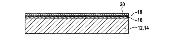
図1〜5に、本発明の製造方法の有利な実施形態による薄膜電池10の構成をステップごとに示す。図1に、半導体基板12として形成された基板14と、該基板14上に設けられた(成膜された)絶縁層16とを示す。この絶縁層16上にはまず、集電層である第1の層18を成膜する。次に、この第1の層18に第2の層20を成膜する。この第2の層20は、たとえばLiCOO2から成り、薄膜電池10のカソード層を成す。これら最初の2つの層18,20は、同図中では別個にパターニングされず、一緒にパターニングされる。
1 to 5 show the configuration of a
図2に、次に行われる前記最初の2つの層18,20のパターニングを示す。図中にないレーザ切断用のレーザ装置の適切なパラメータにより、レーザビームによって、最初の2つの層18,20の層厚さにわたって、ないしは第2の層の層厚さにわたって延在する切り込み22を入れ、この切り込みによって、製造すべき電池10のカソード領域28が電気的に露出され、他の領域24,26から横方向に分離されるようにすることができる。その際に、その下にある集電層18の複数の領域30,32,34も‐少なくとも切り込み22の一部において‐横方向に相互に分離される。この分離は図中の実施例では、第2の層(カソード層)20の複数の領域の分離と同時に行われる。場合によってはオプションとして、コンタクト領域24を別のパラメータによって、活性カソード材料から分離することができる。ただしその場合には、集電層(第1の層18)を絶対に損傷してはならない。すなわち導電性に維持しなければならない。これに相応する場所を、図2においてマークMによって示している。
FIG. 2 shows the next patterning of the first two
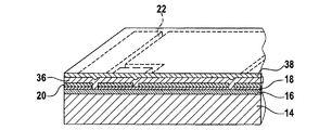
図3に、第2の層20上に成膜された第3の層36と、該第3の層36上に成膜された第4の層38とを示す。この第3の層36は電解質層として形成され、第4の層38はアノード層として形成されている。ここでも、埋め込まれた層のパターニングは行わない。さらに、カソード層のパターニング部を破線で示す。このパターニング部も埋め込まれている。
FIG. 3 shows a
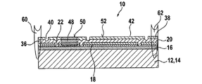
後続のパターニングステップにおいて、複数の領域42,44,46を分離するために、レーザビームによって第4の層38に切り込み40を入れる。このレーザパターニングにより、第4の層38(アノード層)をレーザビームによって適切なパラメータで選択的に、該第4の層38の下にある第3の層36(電解質層)まで切断し、電池10のアノード領域42を該第4の層38の他の領域44,46から電気的に絶縁する。このことは図4に示されている。電気的に絶縁された第2の領域46が電池パターニング部上に設けられ、これによって後のステップにおいて、埋め込まれた第1の層18(集電層)とのコンタクトが形成される(ここでは点線で示されている)。
In a subsequent patterning step, a
アノード材料に応じて、アノード層(第4の層38)の直接的なコンタクトが可能であるか、または、アノード層を適切な材料によってコーティングしなければならない。カソード層(第2の層20)のコンタクトを行うためには、カソード領域において適切な材料をたとえばレーザによって局所的に加熱し、この材料を電解質層(第3の層36)およびカソード層(第2の層20)に拡散させることにより、導電スルーコンタクト48(接続ビア)を形成する。アノード層(第4の層38)がまだ適切な材料から形成されていない場合には、たとえば適切なペーストを塗布して加熱することができる。カソードのコンタクト面50とアノードのコンタクト面52とが形成される。最後に、オプションとして電池10にパッシベーション層を設けることにより(図示していない)、電池の寿命を延長することができる。このパッシベーション層に対応して、カソードおよびアノードのコンタクトを適合しなければならない。
Depending on the anode material, direct contact of the anode layer (fourth layer 38) is possible, or the anode layer must be coated with a suitable material. In order to make contact with the cathode layer (second layer 20), a suitable material is heated locally in the cathode region, for example by means of a laser, and this material is brought into contact with the electrolyte layer (third layer 36) and the cathode layer (second layer). The conductive through contact 48 (connection via) is formed by diffusing into the second layer 20). If the anode layer (fourth layer 38) is not yet formed from a suitable material, for example, a suitable paste can be applied and heated. A
図5に、上述の場合に埋め込まれるカソード層のコンタクトを「レーザ焼結」によって、すなわち、絶縁されたボンディングパッド領域46の局所加熱によって行うのが示されている。温度上昇により、たとえばこの領域にも存在する上側の金属または別個に塗布されたペーストの拡散が活性化し、電解質層に局所的にドーピングされる。このようにして、両電極層(第2の層20および第4の層38)を上側からコンタクトすることができる。図中に示していない別の実施形態として、下方の電極層(第2の層20)のコンタクトを横方向に行い、たとえば、基板14に挿入されるかまたは挿入処理された回路を介して下方の電極層(第2の層20)のコンタクトを行うか、または、基板裏面からコンタクトを行うために基板14に設けられたスルーコンタクト(ビア)を介して、下方の電極層(第2の層20)のコンタクトを行う。導電度に応じて、基板12自体を給電線として使用することができる。ただし、直列抵抗の如何にかかわらず、電池10の出力値は低下する。別の実施形態では、第4の層(アノード層38)を設ける前に第3の層(電解質層)36を選択的に除去し、このように選択的除去を行わないと埋め込まれてしまう層を露出させてコンタクトできるようにする。パッシベーション層を設ける場合には、コンタクト工程を相応に適合しなければならない。
FIG. 5 shows the contact of the cathode layer embedded in the above case by “laser sintering”, ie by local heating of the insulated
本発明の方法はマスキング手法に依存しないことにより、基板14も任意のトポグラフィで(たとえば深いトレンチや孔)でパターニングすることができる。このことはとりわけ、図6に示された3次元薄膜電池54の製造においても有利である。レーザパターニングは、マスクや、パターニング前の基板14の状態に依存しないので、場合によっては成膜をパターニングに適合する必要はなく、基板14に適合すればよくなることがある。3次元薄膜電池54の基板14は、たとえば相互に平行な複数のトレンチ58を有する3次元パターニングされた基板56であり、このような複数のトレンチ58によって、3次元に折り曲げられた薄膜電池(3次元薄膜電池54)を得ることができる。
Since the method of the present invention does not depend on the masking technique, the
層16,18,20,36,38をプリパターニングすることにより、結果的に、たとえばソーイング時に電池材料が間を塞ぐことによって短絡が発生する危険性が生じることなく、電池10個体を分離することができる。機能領域は、半導体基板12の縁部から絶縁される。図中ではアノードの切断線60は、カソード断面の切断線62より若干外側にある。切り込み22,40を適切に配置することにより、たとえば、電解質等を貫通する最初のレーザパターニング時に材料が反ることに起因して発生する短絡を回避することもできる。
By pre-patterning the
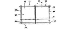
図7に、電池10のダイシング時の基板14を示す。ここで重要なのは、レーザパターニングによるソーイング時に短絡を高信頼性で防止できることである。
FIG. 7 shows the
択一的に‐障害となる反りを生じさせることなく下方の層を適切にパターニングする際には‐薄膜電池の上方の層(第4の層38)に切り込みのみを入れるステップによっても、アノードのパターニングを行うことができる。このようにしてこの第4の層38に得られた領域が、アノードのコンタクト面52を有するアノード領域42であり、他の領域は、カソード領域28において該アノードの下方に配置されたカソードのコンタクト領域50である。
Alternatively, when appropriately patterning the lower layer without causing an obstructing warp, the step of making a cut only in the upper layer (fourth layer 38) of the thin film cell can also Patterning can be performed. The region thus obtained in the
図8に、高感度のLiイオン含有層がソーイングまで上方の金属層または第1のパッシベーション層によって保護される実施形態を示す。上方の層(第4の層38)と金属層またはパッシベーション層とに線64に沿って所期のように切り込みを入れ、その後に、個々の電池10の構造全体の部分を線66に沿ってソーイングによってダイシングすることにより、電池10が完成する。このことにより、埋め込まれた層のパターニングによって、ソーイング時に短絡が発生しないことが保証される。その後に、(別の)パッシベーション層(たとえばAl2O3をALD:原子層成膜法によって)設けることができる。
FIG. 8 shows an embodiment in which a highly sensitive Li ion containing layer is protected by an upper metal layer or first passivation layer until sawing. The upper layer (fourth layer 38) and the metal or passivation layer are cut as expected along
もちろんこの構成を別の順序で、すなわち、埋め込まれたアノード層と、該アノード層の上方に設けられるカソード層とによって実現することもできる。 Of course, this configuration can also be realized in a different order, ie with an embedded anode layer and a cathode layer provided above the anode layer.
基板として考えられる材料は多数存在し、ここで重要なのは、層の成膜時に必要な温度に対して耐性を有することであり、場合によっては、レーザパターニング時の選択性が十分であることも重要になることがある。この材料の例を以下に挙げる:
・シリコン基板。場合によっては、集積回路または集積マイクロメカニカル素子が集積されたシリコン基板、または、スルーコンタクトが設けられたシリコン基板。
・ガラス基板。場合によっては、スルーコンタクトが集積されたガラス基板。
・セラミック
・温度安定性のポリマー。
There are a number of materials that can be considered as substrates, and what is important here is that they are resistant to the temperatures required when depositing layers, and in some cases it is also important to have sufficient selectivity during laser patterning May be. Examples of this material are given below:
-Silicon substrate. In some cases, a silicon substrate on which integrated circuits or integrated micromechanical elements are integrated, or a silicon substrate on which through contacts are provided.
・ Glass substrate. In some cases, a glass substrate with integrated through contacts.
・ Ceramic ・ Temperature stable polymer.
薄膜電池の個々の機能平面(たとえば集電部、カソード、電解質、アノード、集電部、パッシベーション。図1を参照されたい)は連続的に設けられ、とりわけ成膜される。適切な手法によって処理することにより、典型的には、適合された波長、出力、パルス長、パルス周波数および/または書き込み速度でレーザ手法によって処理することにより、絶縁切り込み部が各層に設けられる。通常はこの絶縁切り込みは、次の層が設けられる前に設けられる。その目的は、所望の層を横方向に高信頼性で絶縁し、かつ、その下にある層を場合によっては損傷したり、下の層の機能を阻害しないようにすることである。 The individual functional planes of the thin-film battery (eg current collector, cathode, electrolyte, anode, current collector, passivation, see FIG. 1) are provided continuously and in particular are deposited. By processing by an appropriate technique, an insulating cut is typically provided in each layer by processing by a laser technique at an adapted wavelength, power, pulse length, pulse frequency and / or writing speed. Usually, this insulation notch is provided before the next layer is provided. The purpose is to reliably isolate the desired layer laterally and not damage the underlying layer or possibly impede the function of the underlying layer.
レーザ手法を実施する場合、パターニングをインシチュで行うこともでき、たとえば成膜設備のチャンバの適切な光学窓を通して行うこともできる。切断時に剥離した粒子によってチャンバが汚染されることは、たとえばチャンバの真空排気または保護ガスリンス等の適切な手段によって阻止することができる。 When implementing a laser technique, patterning can also be done in situ, for example through a suitable optical window in the chamber of the deposition facility. Contamination of the chamber with delaminated particles during cutting can be prevented by suitable means such as evacuating the chamber or rinsing a protective gas.
レーザパターニングは基板状態に依存しない。すなわち、たとえばプリパターニングされた基板を大きなトポグラフィで処理することができる(3D薄膜電池)。 Laser patterning does not depend on the substrate state. That is, for example, a pre-patterned substrate can be processed with a large topography (3D thin film battery).
以下の利点が得られる:
・とりわけ遮蔽マスクと比較して、層のパターニングを格段に良好に行えるようになること。基板上(とりわけウェハ上)におけるスペースを格段に効率的に利用し、切断くずを低減することができる。
The following benefits are obtained:
-The patterning of the layer can be performed much better, especially compared to a shielding mask. Space on the substrate (especially on the wafer) can be used remarkably efficiently, and cutting waste can be reduced.
・簡単な絶縁ステップに限定することにより、基板平面のパターニングをたとえば数分以内で行い、たとえばリソグラフィ法および別個のエッチング法を行う場合と比較して非常に迅速に行うことができる。 By limiting to simple isolation steps, patterning of the substrate plane can be done within a few minutes, for example, very quickly compared to eg lithographic and separate etching methods.
・このパターニングは、基板の実際に除去される領域とのみ相互作用する。遮蔽部分が生じない限り、他の領域のパターンおよび形状は任意に選択することができる。それゆえ、基板に深いパターンまたはスルーホールを設けることができる。 This patterning only interacts with the areas that are actually removed from the substrate. As long as no shielding portion is generated, the pattern and shape of other regions can be arbitrarily selected. Therefore, deep patterns or through holes can be provided in the substrate.
・成膜とパターニングとを分離することにより、たとえばCVD法や遮蔽マスク等、たとえば、完全に平坦に設けられなかった遮蔽マスクで成膜を行う際に発生するようなマスキングも発生しなくなる。 By separating the film formation from the patterning, for example, the masking that occurs when film formation is performed with a shielding mask that is not completely flat, such as a CVD method or a shielding mask, does not occur.
・電池のサイズおよび形状を要件に迅速かつフレキシブルに適合することができ、基板ごとに連続的に適合することも、‐分離容易性を考慮して‐1つの基板で適合することもできる。外部でマスク作製を行うステップは必要なく、レーザプログラミングを変更するだけでよい。 -The size and shape of the battery can be quickly and flexibly adapted to the requirements and can be adapted continuously from one substrate to the next, or in consideration of ease of separation-on one substrate. There is no need for external mask making steps, only laser programming changes.
・層を適切にパターニングすることにより、使用電圧を上昇するために複数の異なる電池を直列接続することが、省スペースで「オンチップ」方式で行えるようになる。 -By appropriately patterning the layers, it is possible to connect a plurality of different batteries in series to increase the working voltage in a space-saving "on-chip" manner.
・インシチュパターニングを行えることにより、真空破壊や、湿度および空気に敏感に反応するリチウム層と、阻害または損傷の原因となる大気との接触がないように、このような電池10を作製することができる。こうするためには、すべての必要な層を場合によっては複数の異なるチャンバ内で成膜できる成膜設備に、光学窓を設けるだけでよい。
Manufacturing such a
12,14 基板(半導体基板)
16 絶縁層
18 第1の層
20 第2の層
22,40 切り込み
24,26,28 分離によって形成された領域
30,32,34 分離によって形成された領域
36 第3の層
38 第4の層
42,44,46 分離によって形成された領域
48 スルーコンタクト
50 カソードのコンタクト面
52 アノードのコンタクト面
56 3次元パターニングされた基板
58 トレンチ
60 アノードの切断線
62 カソードの切断線
12, 14 substrate (semiconductor substrate)
16 Insulating
Claims (7)
前記薄膜電池(10)の積層体を形成するために、基板(14)の基板表面に複数の層(16,18,20,36,38)を連続的に設け、
設けた前記層のうち少なくとも1つの層(18,20,38)の複数の異なる領域(24,26,28;30,32,34;42,44,46)を横方向に相互に分離する製造方法において、
前記複数の異なる領域をレーザビームによって分離し、
前記複数の層のうち1つの層(20,38)はカソード層であり、該複数の層のうち1つの層(38,20)はアノード層であり、
前記カソード層および/または前記アノード層は、前記積層体の埋め込み層(18,20,36)として設け、該カソード層および/または該アノード層と外部とのコンタクトのためにスルーコンタクト(48)を作製することを特徴とする、製造方法。 A method for manufacturing a thin film battery (10), comprising:
In order to form a laminate of the thin film battery (10), a plurality of layers (16, 18, 20, 36, 38) are continuously provided on the substrate surface of the substrate (14),
Manufacturing in which a plurality of different regions (24, 26, 28; 30, 32, 34; 42, 44, 46) of at least one layer (18, 20, 38) of the provided layers are laterally separated from each other. In the method
Separating the plurality of different regions with a laser beam;
One layer (20, 38) of the plurality of layers is a cathode layer, and one layer (38, 20) of the plurality of layers is an anode layer,
The cathode layer and / or the anode layer is provided as a buried layer (18, 20, 36) of the laminate, and a through contact (48) is provided for contact between the cathode layer and / or the anode layer and the outside. A manufacturing method characterized by producing.
・前記第2の層(20)の複数の領域(24,26,28)を横方向に相互に分離するか、または、前記第1の層(18)の複数の領域(30,32,34)を横方向に相互に分離しかつ該第2の層(20)の複数の領域(24,26,28)を横方向に相互に分離するステップと、
・前記第2の層(20)に第3の層(36)を設け、該第3の層(36)に第4の層(38)を設けるステップと、
・前記第4の層(38)の複数の領域(42,44,46)を横方向に相互に分離するか、または、前記第3の層(36)の複数の領域を横方向に分離しかつ該第4の層(38)の複数の領域を横方向に相互に分離するステップ
とを有する、請求項1記載の製造方法。 The first layer (18) is provided on the substrate surface, or provided on the insulating layer (16) provided on the substrate surface, and the second layer (20) is provided on the first layer ( 18)
The plurality of regions (24, 26, 28) of the second layer (20) are laterally separated from each other or the plurality of regions (30, 32, 34) of the first layer (18); ) In the lateral direction and the regions (24, 26, 28) of the second layer (20) in the lateral direction.
Providing a third layer (36) on the second layer (20) and providing a fourth layer (38) on the third layer (36);
-Separate the plurality of regions (42, 44, 46) of the fourth layer (38) from each other in the lateral direction, or separate the plurality of regions of the third layer (36) in the lateral direction. And the step of separating the plurality of regions of the fourth layer (38) from each other in the lateral direction.
Applications Claiming Priority (2)
| Application Number | Priority Date | Filing Date | Title |
|---|---|---|---|
| DE102010029060A DE102010029060A1 (en) | 2010-05-18 | 2010-05-18 | Method for manufacturing thin film battery e.g. lithium ion battery, involves successively applying insulation layer and current collector layers on substrate, and separating different areas from previously applied layers via laser beam |
| DE102010029060.2 | 2010-05-18 |
Publications (3)
| Publication Number | Publication Date |
|---|---|
| JP2011243577A JP2011243577A (en) | 2011-12-01 |
| JP2011243577A5 JP2011243577A5 (en) | 2014-07-24 |
| JP5975605B2 true JP5975605B2 (en) | 2016-08-23 |
Family
ID=44898714
Family Applications (1)
| Application Number | Title | Priority Date | Filing Date |
|---|---|---|---|
| JP2011111705A Expired - Fee Related JP5975605B2 (en) | 2010-05-18 | 2011-05-18 | Thin film battery manufacturing method and thin film battery |
Country Status (5)
| Country | Link |
|---|---|
| JP (1) | JP5975605B2 (en) |
| CN (1) | CN102255102B (en) |
| DE (1) | DE102010029060A1 (en) |
| FR (1) | FR2960346B1 (en) |
| IT (1) | ITMI20110836A1 (en) |
Families Citing this family (9)
| Publication number | Priority date | Publication date | Assignee | Title |
|---|---|---|---|---|
| DE102014209263A1 (en) * | 2014-05-15 | 2015-11-19 | Fraunhofer-Gesellschaft zur Förderung der angewandten Forschung e.V. | Microbattery and method of manufacturing a microbattery |
| TW201622228A (en) * | 2014-08-27 | 2016-06-16 | 應用材料股份有限公司 | Three-dimensional thin film battery |
| DE102015204844A1 (en) * | 2015-03-18 | 2016-09-22 | Robert Bosch Gmbh | Method and device for connecting battery cells and battery pack, battery module, battery and vehicle |
| JP6287946B2 (en) * | 2015-05-08 | 2018-03-07 | トヨタ自動車株式会社 | Method for producing battery laminate |
| FR3039005A1 (en) * | 2015-07-13 | 2017-01-20 | St Microelectronics Tours Sas | AUTOSUPPORTED THIN-FILM BATTERY AND METHOD OF MANUFACTURING SUCH BATTERY |
| DE102016118755B4 (en) | 2015-10-05 | 2019-08-14 | Lpkf Laser & Electronics Ag | 3D thin-film battery and a method and substrate for the production thereof |
| JP6683001B2 (en) * | 2016-05-10 | 2020-04-15 | トヨタ自動車株式会社 | Solid-state battery manufacturing method |
| US10833296B2 (en) | 2017-09-26 | 2020-11-10 | International Business Machines Corporation | Thin film solid-state microbattery packaging |
| US10658702B2 (en) * | 2017-10-02 | 2020-05-19 | International Business Machines Corporation | High-performance thin-film battery with an interfacial layer |
Family Cites Families (7)
| Publication number | Priority date | Publication date | Assignee | Title |
|---|---|---|---|---|
| JP3612018B2 (en) * | 1992-12-04 | 2005-01-19 | 株式会社半導体エネルギー研究所 | Method for manufacturing semiconductor device |
| FR2862437B1 (en) * | 2003-11-14 | 2006-02-10 | Commissariat Energie Atomique | PROCESS FOR MANUFACTURING A LITHIUM MICRO-BATTERY |
| SE0402471D0 (en) * | 2004-10-12 | 2004-10-12 | Anders Lundblad | Electrochemical device |
| CA2658092A1 (en) * | 2006-07-18 | 2008-01-24 | Cymbet Corporation | Method and apparatus for solid-state microbattery photolithographic manufacture, singulation and passivation |
| CN101496218A (en) * | 2006-07-25 | 2009-07-29 | 皇家飞利浦电子股份有限公司 | Method for the manufacture of a thin-layer battery stack on a three-dimensional substrate |
| KR101773498B1 (en) * | 2007-10-25 | 2017-09-01 | 어플라이드 머티어리얼스, 인코포레이티드 | Method for high volume manufacturing of thin film batteries |
| FR2952477B1 (en) * | 2009-11-06 | 2011-12-09 | St Microelectronics Tours Sas | METHOD FOR FORMING THIN-FILM LITHIUM-ION BATTERY |
-
2010
- 2010-05-18 DE DE102010029060A patent/DE102010029060A1/en not_active Ceased
-
2011
- 2011-05-13 IT IT000836A patent/ITMI20110836A1/en unknown
- 2011-05-17 CN CN201110127423.6A patent/CN102255102B/en active Active
- 2011-05-17 FR FR1154261A patent/FR2960346B1/en not_active Expired - Fee Related
- 2011-05-18 JP JP2011111705A patent/JP5975605B2/en not_active Expired - Fee Related
Also Published As
| Publication number | Publication date |
|---|---|
| CN102255102A (en) | 2011-11-23 |
| JP2011243577A (en) | 2011-12-01 |
| ITMI20110836A1 (en) | 2011-11-19 |
| FR2960346B1 (en) | 2019-08-23 |
| CN102255102B (en) | 2016-03-23 |
| FR2960346A1 (en) | 2011-11-25 |
| DE102010029060A1 (en) | 2011-11-24 |
Similar Documents
| Publication | Publication Date | Title |
|---|---|---|
| JP5975605B2 (en) | Thin film battery manufacturing method and thin film battery | |
| CN102263293B (en) | For the method and apparatus manufacturing sheet cell group | |
| KR102413942B1 (en) | Deposition of passivation layer on graphene sheet | |
| CN110088904A (en) | Three-dimensional storage part and its manufacturing method | |
| US10903525B2 (en) | Self-supporting thin-film battery and method of manufacturing such a battery | |
| US10373766B2 (en) | Method of producing a super-capacitor | |
| JP2009152186A (en) | Enclosed lithium electrochemical device | |
| JP2017526143A (en) | Laser patterned thin film battery | |
| JP6328131B2 (en) | Capacitive micromachine transducer and manufacturing method thereof | |
| TW201532298A (en) | Solar cell emitter region fabrication using self-aligned implant and cap | |
| JP6888985B2 (en) | Laminated miniature thin film battery and its manufacturing method | |
| JP2004146297A (en) | Solid battery | |
| CN103732528B (en) | Silicon residue is eliminated from MEMS cavity bottoms | |
| TWI708388B (en) | Semiconductor structure and method for manufacturing the same | |
| US10109887B1 (en) | 3D-structured solid state battery | |
| CN113795960B (en) | Method for treating a layered structure | |
| CN114420634A (en) | Preparation method of semiconductor device | |
| TWI227527B (en) | Method of manufacturing a semiconductor device | |
| US11522243B2 (en) | Hermetic packaging of a micro-battery device | |
| KR102388206B1 (en) | Method for manufacturing trench capacitor | |
| TWI798910B (en) | Mathod of manufacturing capacitor | |
| US20240046966A1 (en) | Wordline sidewall contacts in 3d nand structures | |
| JP4741549B2 (en) | Manufacturing method of semiconductor device | |
| CN114242655A (en) | Preparation method of semiconductor device | |
| JP2023115493A (en) | capacitor |
Legal Events
| Date | Code | Title | Description |
|---|---|---|---|
| A621 | Written request for application examination |
Free format text: JAPANESE INTERMEDIATE CODE: A621 Effective date: 20140519 |
|
| A521 | Request for written amendment filed |
Free format text: JAPANESE INTERMEDIATE CODE: A523 Effective date: 20140611 |
|
| A977 | Report on retrieval |
Free format text: JAPANESE INTERMEDIATE CODE: A971007 Effective date: 20150218 |
|
| A131 | Notification of reasons for refusal |
Free format text: JAPANESE INTERMEDIATE CODE: A131 Effective date: 20150223 |
|
| A521 | Request for written amendment filed |
Free format text: JAPANESE INTERMEDIATE CODE: A523 Effective date: 20150525 |
|
| A131 | Notification of reasons for refusal |
Free format text: JAPANESE INTERMEDIATE CODE: A131 Effective date: 20150824 |
|
| A521 | Request for written amendment filed |
Free format text: JAPANESE INTERMEDIATE CODE: A523 Effective date: 20151119 |
|
| A131 | Notification of reasons for refusal |
Free format text: JAPANESE INTERMEDIATE CODE: A131 Effective date: 20160229 |
|
| A521 | Request for written amendment filed |
Free format text: JAPANESE INTERMEDIATE CODE: A523 Effective date: 20160524 |
|
| TRDD | Decision of grant or rejection written | ||
| A01 | Written decision to grant a patent or to grant a registration (utility model) |
Free format text: JAPANESE INTERMEDIATE CODE: A01 Effective date: 20160620 |
|
| A61 | First payment of annual fees (during grant procedure) |
Free format text: JAPANESE INTERMEDIATE CODE: A61 Effective date: 20160719 |
|
| R150 | Certificate of patent or registration of utility model |
Ref document number: 5975605 Country of ref document: JP Free format text: JAPANESE INTERMEDIATE CODE: R150 |
|
| R250 | Receipt of annual fees |
Free format text: JAPANESE INTERMEDIATE CODE: R250 |
|
| R250 | Receipt of annual fees |
Free format text: JAPANESE INTERMEDIATE CODE: R250 |
|
| LAPS | Cancellation because of no payment of annual fees |