JP5966577B2 - Temperature compensation circuit, circuit device, electronic device and adjustment method - Google Patents
Temperature compensation circuit, circuit device, electronic device and adjustment method Download PDFInfo
- Publication number
- JP5966577B2 JP5966577B2 JP2012106459A JP2012106459A JP5966577B2 JP 5966577 B2 JP5966577 B2 JP 5966577B2 JP 2012106459 A JP2012106459 A JP 2012106459A JP 2012106459 A JP2012106459 A JP 2012106459A JP 5966577 B2 JP5966577 B2 JP 5966577B2
- Authority
- JP
- Japan
- Prior art keywords
- order
- circuit
- signal
- order component
- temperature
- Prior art date
- Legal status (The legal status is an assumption and is not a legal conclusion. Google has not performed a legal analysis and makes no representation as to the accuracy of the status listed.)
- Active
Links
Images


Landscapes
- Oscillators With Electromechanical Resonators (AREA)
Description
本発明は、温度補償回路、回路装置、電子機器及び調整方法等に関する。 The present invention relates to a temperature compensation circuit, a circuit device, an electronic device, an adjustment method, and the like.
特許文献1には、0次〜n次信号発生回路が、近似的な0次〜n次関数の信号をそれぞれ発生し、0次〜n次成分ゲイン調整回路が、0次〜n次関数の信号のゲイン調整をそれぞれ行い、加算回路が、ゲイン調整された0次〜n次関数の信号を加算して温度補償用電圧を出力し、その温度補償用電圧により、水晶発振回路の発振周波数がもつ温度特性を補償する技術が開示されている。
In
しかしながら上記の手法では、信号発生回路及びゲイン調整回路が次数毎に独立に構成されている。そのため、温度補償の精度を上げるためには、高次(例えば4次以上)の信号発生回路及びゲイン調整回路の数を増やしていく必要があり、高次の温度補償が複雑になるという課題がある。 However, in the above method, the signal generation circuit and the gain adjustment circuit are configured independently for each order. Therefore, in order to increase the accuracy of temperature compensation, it is necessary to increase the number of higher-order (for example, fourth-order or higher) signal generation circuits and gain adjustment circuits, and there is a problem that higher-order temperature compensation becomes complicated. is there.
本発明の幾つかの態様によれば、簡素な構成で高次の温度補償を行うことが可能な温度補償回路、回路装置、電子機器及び調整方法等を提供できる。 According to some aspects of the present invention, it is possible to provide a temperature compensation circuit, a circuit device, an electronic device, an adjustment method, and the like that can perform high-order temperature compensation with a simple configuration.
本発明の一態様は、温度センサーからの検出信号に基づいて、温度に対する1次関数を近似する信号である1次成分信号を出力する1次成分発生回路と、前記検出信号に基づいて、前記温度に対する3次関数を近似する信号である3次成分信号を出力する3次成分発生回路と、前記検出信号に基づいて、前記温度に対する高次関数を近似する信号である高次成分信号を出力する高次成分発生回路と、前記1次成分信号のゲイン調整を行い、ゲイン調整後の前記1次成分信号を1次出力信号として出力する1次成分ゲイン調整回路と、前記3次成分信号のゲイン調整を行い、ゲイン調整後の前記3次成分信号を3次出力信号として出力する3次成分ゲイン調整回路と、前記高次成分信号のゲイン調整を行い、ゲイン調整後の前記高次成分信号を高次出力信号として出力する高次成分ゲイン調整回路と、前記1次出力信号と前記3次出力信号と前記高次出力信号とを加算し、加算により得られた電圧を温度補償用電圧として出力する加算回路と、を含み、前記高次成分発生回路は、3次関数よりも高次のi次関数(iは4以上の自然数)と、前記i次関数よりも高次のj次関数(jはj>iの自然数)と、が少なくとも合成された合成関数を近似する信号を、前記高次成分信号として出力する温度補償回路に関係する。 One aspect of the present invention is a first-order component generation circuit that outputs a first-order component signal that is a signal that approximates a first-order function with respect to a temperature based on a detection signal from a temperature sensor, and based on the detection signal, A third-order component generation circuit that outputs a third-order component signal that is a signal that approximates a third-order function with respect to temperature, and a higher-order component signal that is a signal that approximates a higher-order function with respect to the temperature, based on the detection signal A high-order component generation circuit that performs gain adjustment of the primary component signal, and outputs the primary component signal after gain adjustment as a primary output signal; and A third-order component gain adjustment circuit that performs gain adjustment and outputs the third-order component signal after gain adjustment as a third-order output signal; and the higher-order component signal after gain adjustment by performing gain adjustment of the higher-order component signal The A high-order component gain adjustment circuit that outputs as a secondary output signal, the primary output signal, the tertiary output signal, and the high-order output signal are added, and a voltage obtained by the addition is output as a temperature compensation voltage. The higher-order component generation circuit includes a higher-order i-order function (i is a natural number of 4 or more) than a cubic function and a higher-order j-order function (j Is a natural number of j> i), and is related to a temperature compensation circuit that outputs a signal that approximates at least a synthesized function synthesized as the higher-order component signal.
本発明の一態様によれば、3次関数よりも高次のi次関数と、i次関数よりも高次のj次関数と、が少なくとも合成された合成関数の信号が、高次成分信号として出力される。そして、ゲイン調整された1次成分信号と、ゲイン調整された3次成分信号と、ゲイン調整された高次成分信号と、が加算されて温度補償用電圧として出力される。これにより、簡素な構成で高次の温度補償を行うことが可能になる。 According to one aspect of the present invention, a composite function signal in which at least an i-order function higher than a cubic function and a j-order function higher than an i-order function are combined is a high-order component signal. Is output as Then, the gain-adjusted primary component signal, the gain-adjusted tertiary component signal, and the gain-adjusted higher-order component signal are added and output as a temperature compensation voltage. This makes it possible to perform high-order temperature compensation with a simple configuration.
また本発明の一態様では、前記高次成分発生回路は、前記i次関数と、前記j次関数と、1次以上3次以下の関数であるm次関数(mは1≦m≦3の自然数)と、が少なくとも合成された前記合成関数を近似する信号を、前記高次成分信号として出力してもよい。 In one embodiment of the present invention, the high-order component generation circuit includes the i-th order function, the j-th order function, and an m-order function that is a function of 1st order to 3rd order (where m is 1 ≦ m ≦ 3). A signal approximating the synthesis function synthesized with at least a natural number may be output as the higher-order component signal.
また本発明の一態様では、前記高次成分発生回路は、前記i次関数と、前記j次関数と、前記j次関数よりも高次のk次関数(kはk>jの自然数)と、が少なくとも合成された前記合成関数を近似する信号を、前記高次成分信号として出力してもよい。 In one embodiment of the present invention, the high-order component generation circuit includes the i-order function, the j-order function, and a k-order function higher than the j-order function (k is a natural number of k> j), A signal approximating the synthesis function synthesized at least may be output as the higher-order component signal.
これら本発明の一態様によれば、温度補償対象デバイスの温度特性の高次成分が、i次関数及びj次関数のみでは高精度に補償できない場合であっても、高次成分信号に対して更にm次関数又はk次関数を合成することで、高次成分の補償精度を向上できる。 According to these aspects of the present invention, even if the high-order component of the temperature characteristic of the temperature compensation target device cannot be compensated with high accuracy only by the i-th order function and the j-th order function, Furthermore, the accuracy of compensation of higher-order components can be improved by synthesizing m-order functions or k-order functions.
また本発明の一態様では、前記高次成分発生回路は、前記1次成分ゲイン調整回路によりゲイン調整された前記1次成分信号と、前記3次成分ゲイン回路によりゲイン調整された前記3次成分信号とにより温度補償対象デバイスの温度特性を補償した場合の残留成分を近似する関数の信号を、前記高次成分信号として出力してもよい。 In one aspect of the present invention, the high-order component generation circuit includes the primary component signal gain-adjusted by the primary-component gain adjustment circuit and the third-order component gain-adjusted by the third-order component gain circuit. A signal of a function that approximates the residual component when the temperature characteristic of the temperature compensation target device is compensated by the signal may be output as the high-order component signal.
このようにすれば、ゲイン調整された1次成分信号及びゲイン調整された3次成分信号により温度補償対象デバイスの温度特性を補償した場合の残留成分を、高次成分信号により補償することができる。これにより、1つの高次成分信号により残留成分を高精度に補償することが可能になる。 In this way, the residual component when the temperature characteristic of the temperature compensation target device is compensated by the gain-adjusted primary component signal and the gain-adjusted tertiary component signal can be compensated by the high-order component signal. . As a result, the residual component can be compensated with high accuracy by one high-order component signal.
また本発明の一態様では、前記1次成分ゲイン調整回路のゲイン値と、前記3次成分ゲイン調整回路のゲイン値と、前記高次成分ゲイン調整回路のゲイン値と、が記憶された記憶部を含んでもよい。 In one aspect of the present invention, the storage unit stores the gain value of the first-order component gain adjustment circuit, the gain value of the third-order component gain adjustment circuit, and the gain value of the higher-order component gain adjustment circuit. May be included.
このようにすれば、1次成分ゲイン調整回路のゲイン値と、3次成分ゲイン調整回路のゲイン値と、高次成分ゲイン調整回路のゲイン値を記憶部に書き込むことで、温度補償用電圧の特性を調整することができる。 In this way, by writing the gain value of the first-order component gain adjustment circuit, the gain value of the third-order component gain adjustment circuit, and the gain value of the higher-order component gain adjustment circuit to the storage unit, the temperature compensation voltage Characteristics can be adjusted.
また本発明の一態様では、前記加算回路は、前記1次成分ゲイン調整回路のゲイン値をA1とし、前記3次成分ゲイン調整回路のゲイン値をA3とし、前記高次成分ゲイン調整回路のゲイン値をAhとし、温度をTとし、基準温度をT0とし、αi、αjを所定の係数とし、f(T−T0)を温度Tの関数とする場合に、VCOMP=Ah(αi(T−T0)i+αj(T−T0)j+f(T−T0))+A3(T−T0)3+A1(T−T0)+A0を近似する前記温度補償用電圧を出力してもよい。 In the aspect of the invention, the adder circuit may have a gain value of the first-order component gain adjustment circuit as A1, a gain value of the third-order component gain adjustment circuit as A3, and a gain of the higher-order component gain adjustment circuit. When the value is Ah, the temperature is T, the reference temperature is T0, αi and αj are predetermined coefficients, and f (T−T0) is a function of the temperature T, VCOMP = Ah (αi (T−T0) I + αj (T−T0) j + f (T−T0)) + A3 (T−T0) 3 + A1 (T−T0) + A0 The temperature compensation voltage may be output.
このようにすれば、i次関数とj次関数とが少なくとも合成された合成関数を近似する高次成分信号と、3次関数を近似する3次成分信号と、1次関数を近似する1次成分信号と、0次成分信号とが加算された温度補償用電圧VCOMPを出力することができる。 In this way, a high-order component signal that approximates a composite function in which at least an i-order function and a j-order function are combined, a tertiary component signal that approximates a cubic function, and a primary that approximates a linear function. The temperature compensation voltage VCOMP obtained by adding the component signal and the zeroth-order component signal can be output.
また本発明の一態様では、mを1≦m≦3の自然数とし、αmを所定の係数とする場合に、f(T−T0)=αm(T−T0)mであってもよい。 In one embodiment of the present invention, when m is a natural number of 1 ≦ m ≦ 3 and αm is a predetermined coefficient, f (T−T0) = αm (T−T0) m may be satisfied.
また本発明の一態様では、kをk>j>i≧4の自然数とし、αkを所定の係数とする場合に、f(T−T0)=αk(T−T0)kであってもよい。 In one embodiment of the present invention, when k is a natural number of k>j> i ≧ 4 and αk is a predetermined coefficient, f (T−T0) = αk (T−T0) k may be satisfied. .
これら本発明の一態様によれば、i次関数とj次関数と1次以上3次以下のm次関数とが合成された合成関数を近似する信号を、高次成分信号として出力できる。あるいは、i次関数とj次関数と4次以上でi次及びj次以外のk次成分信号とが合成された合成関数を近似する信号を、高次成分信号として出力できる。 According to these aspects of the present invention, a signal approximating a composite function obtained by combining an i-order function, a j-order function, and an m-order function of 1st order to 3rd order can be output as a high-order component signal. Alternatively, a signal approximating a composite function in which an i-order function, a j-order function, and a fourth-order or higher-order k-order component signal other than the i-th order and j-th order signals can be output as a high-order component signal.
また本発明の一態様では、前記加算回路は、前記1次成分ゲイン調整回路のゲイン値をA1とし、前記3次成分ゲイン調整回路のゲイン値をA3とし、前記高次成分ゲイン調整回路のゲイン値をAhとし、温度をTとし、基準温度をT0とし、αi、αjを所定の係数とし、前記温度補償用電圧をVCOMPとする場合に、VCOMP=Ah(αi(T−T0)i+αj(T−T0)j)+A3(T−T0)3+A1(T−T0)+A0を出力してもよい。 In the aspect of the invention, the adder circuit may have a gain value of the first-order component gain adjustment circuit as A1, a gain value of the third-order component gain adjustment circuit as A3, and a gain of the higher-order component gain adjustment circuit. When the value is Ah, the temperature is T, the reference temperature is T0, αi and αj are predetermined coefficients, and the temperature compensation voltage is VCOMP, VCOMP = Ah (αi (T−T0) i + αj ( T−T0) j ) + A3 (T−T0) 3 + A1 (T−T0) + A0 may be output.
このようにすれば、i次関数とj次関数とが合成された合成関数を近似する高次成分信号と、3次関数を近似する3次成分信号と、1次関数を近似する1次成分信号と、0次成分信号とが加算された温度補償用電圧VCOMPを出力することができる。 In this way, a high-order component signal that approximates a composite function in which an i-order function and a j-order function are combined, a tertiary component signal that approximates a cubic function, and a primary component that approximates a linear function. The temperature compensation voltage VCOMP obtained by adding the signal and the 0th-order component signal can be output.
また本発明の一態様では、前記i次関数及び前記j次関数のうち一方が奇数次関数であり、他方が偶数次関数である場合に、前記高次成分発生回路は、前記奇数次関数を近似する信号である奇数次成分信号を出力する奇数次成分発生回路と、前記偶数次関数を近似する信号である偶数次成分信号を出力する偶数次成分発生回路と、を有し、前記高次成分発生回路は、前記奇数次成分信号と前記偶数次成分信号とが加算された信号を、前記高次成分信号として出力してもよい。 Also, in one aspect of the present invention, when one of the i-th order function and the j-th order function is an odd-order function and the other is an even-order function, the high-order component generation circuit generates the odd-order function. An odd-order component generation circuit that outputs an odd-order component signal that is an approximate signal, and an even-order component generation circuit that outputs an even-order component signal that is a signal that approximates the even-order function. The component generation circuit may output a signal obtained by adding the odd-order component signal and the even-order component signal as the high-order component signal.
このようにすれば、奇数次関数と偶数次関数の合成関数を近似する信号を、高次成分信号として出力することができる。このように奇数次関数と偶数次関数を合成することで、高次成分の調整自由度を向上することができ、温度特性の高次成分に対する補償精度を向上できる。 In this way, a signal approximating the combined function of the odd-order function and the even-order function can be output as a high-order component signal. By synthesizing the odd-order function and the even-order function in this way, the degree of freedom in adjusting the high-order component can be improved, and the compensation accuracy for the high-order component of the temperature characteristic can be improved.
また本発明の一態様では、前記奇数次成分発生回路は、前記温度センサーからの前記検出信号に基づく検出電圧が入力される第1トランジスターと、所定電圧が入力される第2トランジスターとを有し、前記第1トランジスター及び前記第2トランジスターにより差動動作を行う第1差動回路と、前記第1差動回路の出力電圧が入力される第3トランジスターと、前記検出電圧が入力される第4トランジスターとを有し、前記第3トランジスター及び前記第4トランジスターにより差動動作を行い、前記奇数次成分信号を出力する第2差動回路と、を有してもよい。 In the aspect of the invention, the odd-order component generation circuit includes a first transistor to which a detection voltage based on the detection signal from the temperature sensor is input, and a second transistor to which a predetermined voltage is input. A first differential circuit that performs a differential operation by the first transistor and the second transistor, a third transistor to which an output voltage of the first differential circuit is input, and a fourth transistor to which the detection voltage is input. And a second differential circuit that performs a differential operation by the third transistor and the fourth transistor and outputs the odd-order component signal.
このようにすれば、第1差動回路の差動動作により、温度センサーからの検出信号に基づいて出力電圧が出力され、第2差動回路の差動動作により、第1差動回路の出力電圧に基づいて奇数次成分信号が出力される。このようにして、温度センサーからの検出信号に基づいて奇数次成分信号を生成することができる。 According to this configuration, the output voltage is output based on the detection signal from the temperature sensor by the differential operation of the first differential circuit, and the output of the first differential circuit by the differential operation of the second differential circuit. An odd-order component signal is output based on the voltage. In this way, an odd-order component signal can be generated based on the detection signal from the temperature sensor.
また本発明の一態様では、前記偶数次成分発生回路は、前記温度センサーからの前記検出信号に基づく検出電圧が入力される第5トランジスターと、所定電圧が入力される第6トランジスターとを有し、前記第5トランジスター及び前記第6トランジスターにより差動動作を行う第3差動回路と、前記第3差動回路の出力電圧が入力される第7トランジスターと、前記検出電圧が入力される第8トランジスターとを有し、前記第7トランジスター及び第8トランジスターにより差動動作を行う第4差動回路と、前記第7トランジスターの出力電流と、前記第8トランジスターの出力電流とを加算した電流に基づいて、前記偶数次成分信号を出力する出力回路と、を有してもよい。 In the aspect of the invention, the even-order component generation circuit includes a fifth transistor to which a detection voltage based on the detection signal from the temperature sensor is input and a sixth transistor to which a predetermined voltage is input. A third differential circuit that performs a differential operation using the fifth transistor and the sixth transistor; a seventh transistor that receives an output voltage of the third differential circuit; and an eighth that receives the detection voltage. A fourth differential circuit having a transistor and performing a differential operation by the seventh transistor and the eighth transistor, and a current obtained by adding the output current of the seventh transistor and the output current of the eighth transistor And an output circuit for outputting the even-order component signal.
このようにすれば、第3差動回路の差動動作により、温度センサーからの検出信号に基づいて出力電圧が出力され、第4差動回路の差動動作により、第3差動回路の出力電圧に基づいて差動出力電流が出力され、出力回路により、第4差動回路の差動出力電流に基づいて偶数次成分信号が出力される。このようにして、温度センサーからの検出信号に基づいて偶数次成分信号を生成することができる。 According to this configuration, the output voltage is output based on the detection signal from the temperature sensor by the differential operation of the third differential circuit, and the output of the third differential circuit by the differential operation of the fourth differential circuit. A differential output current is output based on the voltage, and an even-order component signal is output by the output circuit based on the differential output current of the fourth differential circuit. In this way, an even-order component signal can be generated based on the detection signal from the temperature sensor.
また本発明の他の態様は、上記のいずれかに記載された温度補償回路と、前記温度補償用電圧により、発振周波数の温度特性が補償される発振回路と、を含む回路装置に関係する。 Another aspect of the present invention relates to a circuit device including any one of the temperature compensation circuit described above and an oscillation circuit in which a temperature characteristic of an oscillation frequency is compensated by the temperature compensation voltage.
また本発明の更に他の態様は、上記に記載された回路装置を含む電子機器に関係する。 Still another embodiment of the present invention relates to an electronic apparatus including the circuit device described above.
また本発明の更に他の態様は、上記のいずれかに記載された温度補償回路が出力する前記温度補償用電圧を調整する調整方法であって、前記1次成分ゲイン調整回路のゲイン値と、前記3次成分ゲイン調整回路のゲイン値とを調整して、温度補償対象デバイスの温度特性を補償し、前記補償された温度特性を、前記高次成分ゲイン調整回路のゲイン値を調整して補償し、前記調整された前記1次成分ゲイン調整回路のゲイン値と、前記3次成分ゲイン調整回路のゲイン値と、前記高次成分ゲイン調整回路のゲイン値とを、前記温度補償回路が有する記憶部に記憶させる調整方法に関係する。 According to still another aspect of the present invention, there is provided an adjustment method for adjusting the temperature compensation voltage output from the temperature compensation circuit described in any of the above, wherein a gain value of the primary component gain adjustment circuit, The gain value of the third-order component gain adjustment circuit is adjusted to compensate for the temperature characteristic of the temperature compensation target device, and the compensated temperature characteristic is compensated by adjusting the gain value of the higher-order component gain adjustment circuit. The temperature compensation circuit stores the adjusted gain value of the first-order component gain adjustment circuit, the gain value of the third-order component gain adjustment circuit, and the gain value of the higher-order component gain adjustment circuit. This relates to the adjustment method stored in the unit.
このようにすれば、1次成分信号及び3次成分信号により温度補償対象デバイスの温度特性を補償し、その補償後の残留成分を、高次成分信号により補償することができる。これにより、温度特性の高次成分を高次成分信号のゲイン値を調整するだけで、簡素に補償することができる。 In this way, the temperature characteristics of the temperature compensation target device can be compensated by the primary component signal and the tertiary component signal, and the compensated residual component can be compensated by the high-order component signal. As a result, the high-order component of the temperature characteristic can be simply compensated only by adjusting the gain value of the high-order component signal.
また本発明の更に他の態様は、上記のいずれかに記載された温度補償回路が出力する前記温度補償用電圧を調整する調整方法であって、前記1次成分ゲイン調整回路のゲイン値と、前記3次成分ゲイン調整回路のゲイン値と、前記高次成分ゲイン調整回路のゲイン値とを調整して、温度補償対象デバイスの温度特性を補償し、前記調整された前記1次成分ゲイン調整回路のゲイン値と、前記3次成分ゲイン調整回路のゲイン値と、前記高次成分ゲイン調整回路のゲイン値とを、前記温度補償回路が有する記憶部に記憶させてもよい。 According to still another aspect of the present invention, there is provided an adjustment method for adjusting the temperature compensation voltage output from the temperature compensation circuit described in any of the above, wherein a gain value of the primary component gain adjustment circuit, Adjusting the gain value of the third-order component gain adjustment circuit and the gain value of the higher-order component gain adjustment circuit to compensate for the temperature characteristics of the temperature compensation target device, and adjusting the adjusted first-order component gain adjustment circuit The gain value of the third-order component gain adjustment circuit and the gain value of the higher-order component gain adjustment circuit may be stored in a storage unit included in the temperature compensation circuit.
このようにすれば、1次成分信号のゲイン値、3次成分信号のゲイン値、高次成分信号のゲイン値を一度に調整することができるため、温度補償用電圧の調整フローを更に簡素化することが可能になる。 In this way, the gain value of the primary component signal, the gain value of the tertiary component signal, and the gain value of the high-order component signal can be adjusted at once, further simplifying the adjustment flow of the temperature compensation voltage. It becomes possible to do.
以下、本発明の好適な実施の形態について詳細に説明する。なお以下に説明する本実施形態は特許請求の範囲に記載された本発明の内容を不当に限定するものではなく、本実施形態で説明される構成の全てが本発明の解決手段として必須であるとは限らない。 Hereinafter, preferred embodiments of the present invention will be described in detail. The present embodiment described below does not unduly limit the contents of the present invention described in the claims, and all the configurations described in the present embodiment are indispensable as means for solving the present invention. Not necessarily.
なお、以下では温度補償対象デバイスが水晶振動子である場合を例に説明するが、本実施形態はこれに限定されず、温度補償対象デバイスは、その発振周波数の温度特性を電圧により補償できるデバイスであればよい。例えば温度補償対象デバイスは圧電振動子であってもよい。 In the following, a case where the temperature compensation target device is a crystal resonator will be described as an example. However, the present embodiment is not limited to this, and the temperature compensation target device is a device that can compensate the temperature characteristics of the oscillation frequency with a voltage. If it is. For example, the temperature compensation target device may be a piezoelectric vibrator.
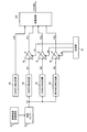
1.温度補償回路
図1に、本実施形態の温度補償回路の構成例を示す。図1の温度補償回路は、温度センサー10、基準温度調整回路15(T0調整回路)、0次成分発生回路20、1次成分発生回路30、3次成分発生回路40、高次成分発生回路50、1次成分ゲイン調整回路60、3次成分ゲイン調整回路70、高次成分ゲイン調整回路80、記憶部90、加算回路100を含む。
1. Temperature Compensation Circuit FIG. 1 shows a configuration example of the temperature compensation circuit of the present embodiment. 1 includes a
温度センサー10は、温度の検出結果を温度検出電圧VT(広義には検出信号)として出力する。基準温度調整回路15は、温度補償用電圧VCOMPの基準温度T0を調整する回路であり、例えば温度検出電圧VTの基準電圧を調整することで基準温度T0を調整する。温度補償用電圧VCOMPの1次成分、3次成分、高次成分は、それぞれ基準温度T0を中心に対称であり、基準温度調整回路15は、その対称の中心を調整する。温度センサー10、基準温度調整回路15の詳細については図5等で後述する。
The
0次成分発生回路20は、水晶振動子(広義には温度補償対象デバイス)の発振周波数がもつ温度特性の0次成分を近似する0次成分電圧VS0(広義には0次成分信号)を出力する。例えば抵抗分割回路など、DC電圧を出力する回路で構成される。
The zero-order
1次成分発生回路30は、水晶振動子の発振周波数がもつ温度特性の1次成分を近似する1次成分電流IS1(広義には1次成分信号)を出力する。即ち、Tを温度とすると、IS1は、(T−T0)に比例又は反比例する関数を近似する電流である。1次成分発生回路30は、例えば正転増幅アンプ等により構成できる。1次成分ゲイン調整回路60は、記憶部90に記憶されたゲイン値A1に基づいて、1次成分電流IS1のゲイン調整を行い、1次成分電圧VS1=A1×IS1(広義には1次出力信号)を出力する。なお、1次成分発生回路30及び1次成分ゲイン調整回路60は、ゲイン調整可能な一体のアンプ回路(例えば正転増幅アンプ)として構成されてもよい。
The primary
3次成分発生回路40は、水晶振動子の発振周波数がもつ温度特性の3次成分を近似する3次成分電流IS3(広義には3次成分信号)を出力する。即ち、IS3は、(T−T0)3に比例又は反比例する関数を近似する電流である。3次成分ゲイン調整回路70は、記憶部90に記憶されたゲイン値A3に基づいて、3次成分電流IS3のゲイン調整を行い、3次成分電圧VS3=A3×IS3(広義には3次出力信号)を出力する。
The third-order
高次成分発生回路50は、水晶振動子の発振周波数がもつ温度特性の、4次以上の成分である高次成分を近似する高次成分電流ISh(広義には高次成分信号)を出力する。即ち、IShは高次関数g(T−T0)を近似する電流である。iをi≧4の自然数、jをj>iの自然数とすると、g(T−T0)は、i次関数(T−T0)iに比例又は反比例する関数、及びj次関数(T−T0)jに比例又は反比例する関数を少なくとも合成した合成関数である。高次成分ゲイン調整回路80は、記憶部90に記憶されたゲイン値Ahに基づいて、高次成分電流IShのゲイン調整を行い、高次成分電圧VSh=Ah×ISh(広義には高次出力信号)を出力する。高次成分発生回路50、高次成分ゲイン調整回路80の詳細については図8等で後述する。
The high-order
加算回路100は、0次成分電圧VS0、1次成分電圧VS1、3次成分電圧VS3、高次成分電圧VShを加算し、温度補償用電圧VCOMPを出力する。VCOMPは、例えば図20で後述する発振回路の可変容量キャパシターC1に入力され、VCOMPによりC1の容量が調整されることで水晶振動子XTALの発振周波数が温度補償される。VS0=A0とすると、温度補償用電圧VCOMPは下式(1)を近似する電圧である。
VCOMP=Ah×g(T−T0)+
A3(T−T0)3+A1(T−T0)+A0 (1)
The
VCOMP = Ah × g (T−T0) +
A3 (T−T0) 3 + A1 (T−T0) + A0 (1)
記憶部90には、例えば温度補償型水晶発振器(TCXO: Temperature Compensated crystal(X) Oscillator)の製造工程で調整された、ゲイン値A0、A1、A3、Ah及び基準温度T0が格納されている。記憶部90は、例えば不揮発性メモリー(例えばEEPROM)により構成される。
The
なお、図1の構成例では、1次成分信号として電流IS1が出力され、3次成分信号として電流IS3が出力され、高次成分信号として電流IShが出力される場合を例に説明したが、本実施形態はこれに限定されない。即ち、1次成分信号、3次成分信号、高次成分信号として電圧が出力されるように構成してもよい。 In the configuration example of FIG. 1, the case where the current IS1 is output as the primary component signal, the current IS3 is output as the tertiary component signal, and the current ISh is output as the high order component signal has been described as an example. The present embodiment is not limited to this. That is, the voltage may be output as a primary component signal, a tertiary component signal, or a high-order component signal.
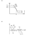
さて、図2に、水晶振動子の発振周波数がもつ温度特性の一例を示す。この温度特性の変動範囲を、温度補償により、例えば±0.5ppm(parts per million)の範囲に収めたいとする。図3に示すように、0次成分、1次成分、3次成分のゲイン値A0、A1、A3を調整し、基準温度T0付近(例えばT0=25度の付近0度〜50度)の温度特性を補償したとする。この場合、B1、B2に示すように、補償したい温度範囲(例えば−30度〜80度)の端では、発振周波数の変動が±0.5ppmを超えてしまう。このような±0.5ppmを超えた部分については、4次以上の高次成分により補償する必要があり、補償精度を上げるほどより高次の補償が必要となる。 FIG. 2 shows an example of temperature characteristics of the oscillation frequency of the crystal resonator. It is assumed that the fluctuation range of the temperature characteristic is desired to be within a range of ± 0.5 ppm (parts per million) by temperature compensation, for example. As shown in FIG. 3, the gain values A0, A1, and A3 of the zeroth-order component, the first-order component, and the third-order component are adjusted, and the temperature near the reference temperature T0 (for example, near 0 to 50 degrees where T0 = 25 degrees). Assume that the characteristics are compensated. In this case, as indicated by B1 and B2, the fluctuation of the oscillation frequency exceeds ± 0.5 ppm at the end of the temperature range to be compensated (for example, −30 degrees to 80 degrees). Such a portion exceeding ± 0.5 ppm needs to be compensated by a higher-order component of the fourth or higher order, and higher-order compensation is required as the compensation accuracy is increased.
従来の温度補償回路では、高次の次数を増やして補償精度を上げるためには、高次の補償回路を多数用意する必要があった。例えば、温度調整回路が、4次成分発生回路、4次成分ゲイン調整回路、5次成分発生回路、5次成分ゲイン調整回路を含み、水晶振動子と発振回路装置(IC)を組み立て製造するときに、4次成分ゲイン値と5次成分ゲイン値を調整する必要があった。この例では、高次の補償回路として4ブロックの回路が必要であり、製造時のパラメーター調整も2つのパラメーターを調整する必要がある。この回路ブロック数やパラメーター数は、補償精度を上げるほど多くなり、回路構成や調整手法が複雑化するという課題がある。 In the conventional temperature compensation circuit, in order to increase the high-order order and increase the compensation accuracy, it is necessary to prepare a large number of high-order compensation circuits. For example, when the temperature adjustment circuit includes a quaternary component generation circuit, a quaternary component gain adjustment circuit, a quintic component generation circuit, and a quintic component gain adjustment circuit, and assembles and manufactures a crystal resonator and an oscillation circuit device (IC) In addition, it is necessary to adjust the fourth-order component gain value and the fifth-order component gain value. In this example, a four-block circuit is required as a high-order compensation circuit, and parameter adjustment at the time of manufacturing also requires adjustment of two parameters. There is a problem that the number of circuit blocks and the number of parameters increase as the compensation accuracy increases, and the circuit configuration and adjustment method become complicated.
この点、本実施形態によれば、高次成分発生回路50と高次成分ゲイン調整回路80の2つの回路ブロックにより高次成分電圧VShを発生し、1つのゲイン値Ahを調整することで、温度特性がもつ4次以上の高次成分を補償することができる。これにより、高次補償回路の回路構成や調整手法を簡素化でき、高次の次数を増やして補償精度を上げる場合であっても、回路構成や調整手法の複雑化を避けることができる。
In this regard, according to the present embodiment, the high-order component voltage VSh is generated by the two circuit blocks of the high-order
具体的には、図2で説明した温度特性は、同一製品の水晶振動子ではおおよそ同一の特性であり、図3で説明した高次の残留成分についても、同一製品の水晶振動子ではおおよそ同一の特性となる。そのため、温度補償回路の設計段階において、高次成分電圧VShの特性を、高次の残留成分の特性に合わせて設計しておくことができ、製造時の調整段階において1つのゲイン値Ahだけで高次成分を補償することが可能となる。 Specifically, the temperature characteristics described with reference to FIG. 2 are approximately the same for the crystal resonator of the same product, and the higher-order residual components described with reference to FIG. 3 are also approximately the same for the crystal resonator of the same product. It becomes the characteristic. Therefore, the characteristic of the high-order component voltage VSh can be designed in accordance with the characteristic of the high-order residual component in the design stage of the temperature compensation circuit, and only one gain value Ah can be used in the adjustment stage during manufacturing. Higher order components can be compensated.
本実施形態において高次成分を補償する高次成分電圧VShは、上式(1)のAh×g(T−T0)である。合成関数g(T−T0)は、例えば下式(2)を近似する関数である。iはi≧4の自然数であり、jはj>iの自然数である。αi、αjは、高次関数の形状を決める所定の係数であり、高次成分発生回路50の設計パラメーター(例えば、後述する図9のトランジスターTR1〜TR4のサイズ、バイアス電流IB1、IB2の電流値など)によって決まる。
g(T−T0)=αi(T−T0)i+αj(T−T0)j (2)
In the present embodiment, the high-order component voltage VSh that compensates the high-order component is Ah × g (T−T0) in the above equation (1). The composite function g (T−T0) is a function that approximates the following equation (2), for example. i is a natural number of i ≧ 4, and j is a natural number of j> i. αi and αj are predetermined coefficients that determine the shape of the high-order function, and are design parameters of the high-order component generation circuit 50 (for example, the sizes of transistors TR1 to TR4 in FIG. 9 described later, current values of bias currents IB1 and IB2) Etc.).
g (T−T0) = αi (T−T0) i + αj (T−T0) j (2)
上式(2)では、図3に示すような高次の残留成分を2つの高次関数により近似し、その近似高次関数の電圧VShを発生することができる。例えば、i次関数αi(T−T0)i及びj次関数αj(T−T0)jのうち一方は奇数次関数であり、他方は偶数次関数である。奇数次関数は基準温度T0を中心に点対称な関数(例えば図13)であり、偶数次関数は基準温度T0を中心に線対称な関数(例えば図19)である。そのため、奇数次関数と偶数次関数を合成することで、奇数次同士又は偶数次同士を合成した場合よりも関数の形状を調整する自由度が大きくなり、補償精度を向上できる。 In the above equation (2), a high-order residual component as shown in FIG. 3 can be approximated by two high-order functions, and the voltage VSh of the approximate high-order function can be generated. For example, one of the i-th order function αi (T−T0) i and the jth order function αj (T−T0) j is an odd-order function, and the other is an even-order function. The odd-order function is a point-symmetrical function (for example, FIG. 13) about the reference temperature T0, and the even-order function is a line-symmetrical function (for example, FIG. 19) about the reference temperature T0. Therefore, by synthesizing the odd-order function and the even-order function, the degree of freedom for adjusting the shape of the function becomes greater than when the odd-order functions or even-order functions are combined, and the compensation accuracy can be improved.
なお、合成関数g(T−T0)は、下式(3)の関数であってもよい。関数f(T−T0)は、i次及びj次以外の次数をもつ関数で構成されており、3次以下の関数を含んでもよいし、4次以上の高次関数を含んでもよい。
g(T−T0)=αi(T−T0)i+αj(T−T0)j+f(T−T0) (3)
The composite function g (T−T0) may be a function of the following expression (3). The function f (T-T0) is composed of functions having orders other than the i-th order and the j-th order, and may include functions of the third order or lower, and may include higher-order functions of the fourth order or higher.
g (T−T0) = αi (T−T0) i + αj (T−T0) j + f (T−T0) (3)
例えば、mを1≦m≦3の自然数とし、αmを所定の係数とする場合に、関数f(T−T0)は下式(4)の関数である。
f(T−T0)=αm(T−T0)m (4)
For example, when m is a natural number of 1 ≦ m ≦ 3 and αm is a predetermined coefficient, the function f (T−T0) is a function of the following expression (4).
f (T−T0) = αm (T−T0) m (4)
あるいは、関数f(T−T0)は下式(5)の関数であってもよいし、下式(6)の関数であってもよい。kはk>j>i≧4の自然数であり、αkは所定の係数である。
f(T−T0)=αk(T−T0)k (5)
f(T−T0)=αm(T−T0)m+αk(T−T0)k (6)
Alternatively, the function f (T−T0) may be a function of the following expression (5) or a function of the following expression (6). k is a natural number of k>j> i ≧ 4, and αk is a predetermined coefficient.
f (T−T0) = αk (T−T0) k (5)
f (T−T0) = αm (T−T0) m + αk (T−T0) k (6)
水晶振動子の温度特性から0次、1次、3次の成分を除いた高次の成分は、i次とj次の2つの関数のみで完全に近似できるとは限らない。特に、より高精度な補償が必要となった場合、i次とj次の2つの関数のみでは補償できない可能性がある。この点、上式(4)〜(6)によれば、高次成分がi次とj次の2つの関数だけのときよりも複雑な高次成分を出力できるため、水晶振動子の温度特性に対するフィッティング精度を向上でき、より高精度な温度補償が可能になる。基本的には、1次、3次の成分については1次成分電圧VS1と3次成分電圧VS3により補償するが、1次成分電圧VS1と3次成分電圧VS3で補償した後の残留成分を補償するのが高次成分電圧VShである。この残留成分は、主にi次及びj次ではあるが、更にk次成分やm次成分を高次成分電圧VShに追加し、補償の精度を上げることで、高次の補償を残留成分に近づけることができる。このようにk次成分やm次成分などの次数を増やしたとしても、ゲイン調整は高次成分電圧VShに対する1つで良いため、高次の各次数を個別にゲイン調整する場合よりも回路規模の増大を抑制できる。高次成分電圧VShのゲイン調整が1つであるため、高次成分の調整自由度は、高次の各次数を個別にゲイン調整する場合よりも小さくなる。しかしながら、高次の残留成分は水晶振動子の製品固有の温度特性に依存するため、同一製品の各個体の温度特性は相似となり、高次成分を1つのゲインで調整しても十分に高精度な補償が可能となる。 Higher-order components obtained by removing the 0th, 1st, and 3rd order components from the temperature characteristics of the crystal resonator cannot be completely approximated by only two functions of i-th order and j-th order. In particular, when more accurate compensation is required, it may not be possible to compensate only with two functions of i-th order and j-th order. In this regard, according to the above formulas (4) to (6), the higher-order components can be output more complicated than when only the two functions of the i-th order and the j-th order are used. The fitting accuracy can be improved, and more accurate temperature compensation becomes possible. Basically, primary and tertiary components are compensated by primary component voltage VS1 and tertiary component voltage VS3, but residual components after compensation by primary component voltage VS1 and tertiary component voltage VS3 are compensated. It is the high-order component voltage VSh. Although this residual component is mainly of the i-th order and j-th order, the k-th order component and the m-th order component are further added to the higher-order component voltage VSh, and the compensation accuracy is increased, so that the higher-order compensation is made the residual component. You can get closer. Even if the orders of the k-order component and the m-order component are increased in this way, the gain adjustment may be one for the higher-order component voltage VSh, so that the circuit scale is larger than the case where each higher-order order gain is individually adjusted. Can be suppressed. Since there is only one gain adjustment of the high-order component voltage VSh, the degree of freedom of adjustment of the high-order component becomes smaller than that in the case of individually adjusting the gain of each high-order order. However, since the higher-order residual components depend on the temperature characteristics specific to the crystal oscillator product, the individual temperature characteristics of the same product are similar, and even if the higher-order components are adjusted with a single gain, they are sufficiently accurate. Compensation becomes possible.
2.温度補償用電圧VCOMPの調整方法
図4に、本実施形態において温度補償用電圧VCOMPを調整する方法のフローチャートを示す。例えば、この調整フローは、水晶振動子と発振回路IC(広義には回路装置)をパッケージングする組み立て工程において実行される。
2. Adjustment Method of Temperature Compensation Voltage VCOMP FIG. 4 shows a flowchart of a method for adjusting the temperature compensation voltage VCOMP in this embodiment. For example, this adjustment flow is executed in an assembly process for packaging a crystal resonator and an oscillation circuit IC (circuit device in a broad sense).
図4に示すように、調整フローを開始すると、温度槽の温度を測定ポイントに順次設定し、水晶振動子単体の周波数温度特性を取得する(ステップS1)。ステップS1では、測定ポイントは例えば5ポイント等とし、ラフな温度特性を取得する。次に、水晶振動子と、本実施形態の温度補償回路が組み込まれた発振回路ICとを一体にパッケージし、温度補償型水晶発振器TCXOに組み立てる(ステップS2)。 As shown in FIG. 4, when the adjustment flow is started, the temperature of the temperature chamber is sequentially set as a measurement point, and the frequency-temperature characteristic of the crystal unit is acquired (step S1). In step S1, the measurement points are set to 5 points, for example, and rough temperature characteristics are acquired. Next, the crystal resonator and the oscillation circuit IC in which the temperature compensation circuit of this embodiment is incorporated are integrally packaged and assembled into a temperature compensation type crystal oscillator TCXO (step S2).
次に、ステップS1で取得した温度特性を1次関数及び3次関数で近似し、1次成分のゲイン値A1と、3次成分のゲイン値A3と、基準温度T0(図5の電圧VAT0)とを求める(ステップS3)。ステップS3では、温度範囲の中心部分(基準温度T0の周辺)で、最小二乗法による誤差が小さくなるようにA1、A3、T0を決定する。次に、求めたゲイン値A1、A3と、基準温度T0とを記憶部90に書き込む。
Next, the temperature characteristic acquired in step S1 is approximated by a linear function and a cubic function, and the gain value A1 of the primary component, the gain value A3 of the tertiary component, and the reference temperature T0 (voltage VAT0 in FIG. 5). Is obtained (step S3). In step S3, A1, A3, and T0 are determined so that the error by the least square method is reduced at the center of the temperature range (around the reference temperature T0). Next, the obtained gain values A1 and A3 and the reference temperature T0 are written in the
次に、温度槽の温度を測定ポイントに順次設定し、TCXOの温度特性を測定する(ステップS5)。ここで測定される温度特性は、図3で説明したように、温度特性の1次成分と3次成分が補正された後の高次の残留成分である。次に、ステップS5で取得した温度特性を高次関数で近似し、高次成分のゲイン値Ahを求める(ステップS6)。ステップS6では、最小二乗法により、残留成分と高次関数の誤差が小さくなるようにAhを決定する。次に、求めたゲイン値Ahを記憶部90に書き込む(ステップS7)。 Next, the temperature of the temperature bath is sequentially set as a measurement point, and the temperature characteristics of the TCXO are measured (step S5). The temperature characteristic measured here is a high-order residual component after correcting the primary component and the tertiary component of the temperature characteristic as described with reference to FIG. Next, the temperature characteristic acquired in step S5 is approximated by a high-order function to obtain a gain value Ah of a high-order component (step S6). In step S6, Ah is determined by the least square method so that the error between the residual component and the higher-order function is reduced. Next, the obtained gain value Ah is written in the storage unit 90 (step S7).
次に、0次成分電圧A0(VS0)を調整し、決定したA0を記憶部90に書き込む(ステップS8)。A0は、TCXOの発振周波数の絶対値を調整するパラメーターであり、仕様で決められた発振周波数となるようにA0を決定する。 Next, the zero-order component voltage A0 (VS0) is adjusted, and the determined A0 is written in the storage unit 90 (step S8). A0 is a parameter for adjusting the absolute value of the oscillation frequency of the TCXO, and A0 is determined so as to be the oscillation frequency determined by the specification.
図4の調整フローでは、まず、ゲイン値A1、A3及び基準温度T0を調整することにより温度特性の1次成分及び3次成分を補償し、次に、その残留成分である高次成分を、ゲイン値Ahを調整することにより補償する。これにより、温度特性から1次成分及び3次成分を除いた残留成分を、簡素な手法で、即ち1つのゲイン値Ahを調整するだけで、補償することができる。 In the adjustment flow of FIG. 4, first, the first and third order components of the temperature characteristics are compensated by adjusting the gain values A1 and A3 and the reference temperature T0, and then the higher order components that are the residual components are Compensation is performed by adjusting the gain value Ah. As a result, the residual component obtained by removing the primary component and the tertiary component from the temperature characteristic can be compensated by a simple method, that is, only by adjusting one gain value Ah.
なお、本実施形態の調整フローは図4の調整フローに限定されない。例えば、ゲイン値A1、A3、Ah及び基準温度T0を1回の近似計算で求めてもよい。この場合、TCXOの温度特性を、温度補償されていない状態で測定し、その測定された温度特性に対して最小二乗法によりA1、A3、Ah、T0を決定すればよい。このようにすれば、更に簡素な調整フローでパラメーターを決定できる。 Note that the adjustment flow of the present embodiment is not limited to the adjustment flow of FIG. For example, the gain values A1, A3, Ah and the reference temperature T0 may be obtained by one approximate calculation. In this case, the temperature characteristics of the TCXO may be measured without temperature compensation, and A1, A3, Ah, and T0 may be determined by the least square method for the measured temperature characteristics. In this way, parameters can be determined with a simpler adjustment flow.
3.温度センサー
次に、図1で説明した温度調整回路の詳細な構成について説明する。まず、図5に、温度センサー10の詳細な構成例を示す。
3. Next, a detailed configuration of the temperature adjustment circuit described with reference to FIG. 1 will be described. First, FIG. 5 shows a detailed configuration example of the
図5に示すように、温度センサー10は、一端に定電圧VRTが供給される抵抗素子RTと、抵抗素子RTの他端にコレクター端子が接続されるバイポーラトランジスターTRT1と、バイポーラトランジスターTRT1のエミッター端子にコレクター端子が接続されるバイポーラトランジスターTRT2と、を含む。
As shown in FIG. 5, the
バイポーラトランジスターTRT1、TRT2は、それぞれダイオード接続されており、バイポーラトランジスターTRT1のコレクター端子に接続されるノードに、温度特性をもつ電圧VTSQが出力される。電圧VTSQの温度特性は、バイポーラトランジスターTRT1、TRT2のベース−エミッター間電圧の温度依存性によって生じる。図6に示すように、電圧VTSQは、負の勾配をもつ1次の温度特性を有している。 The bipolar transistors TRT1 and TRT2 are diode-connected, and a voltage VTSQ having temperature characteristics is output to a node connected to the collector terminal of the bipolar transistor TRT1. The temperature characteristic of the voltage VTSQ is caused by the temperature dependence of the base-emitter voltage of the bipolar transistors TRT1 and TRT2. As shown in FIG. 6, the voltage VTSQ has a first-order temperature characteristic having a negative gradient.
図5の温度センサー10は、正極入力端子に電圧VTSQが入力される演算増幅器OPAと、基準温度T0を調整する電圧VAT0が一端に供給され、他端が演算増幅器OPAの負極入力端子に接続される抵抗素子RA1と、一端が演算増幅器OPAの負極入力端子に接続され、他端が演算増幅器OPAの出力端子に接続される抵抗素子RA2と、を含む。
In the
演算増幅器OPA及び抵抗素子RA1、RA2は、電圧VAT0を基準として電圧VTSQを正転増幅する増幅アンプを構成しており、温度検出電圧VT=VAT0+(1+RA2/RA1)(VTSQ−VAT0)を出力する。図7に示すように、基準電圧VAT0を例えばVAT0a、VAT0bに調整することにより、基準温度T0をT0aやT0bに調整することができる。基準電圧VAT0を出力する基準温度調整回路15は、例えば、電源電圧VDDとグランド電圧VSSの間を抵抗分割する抵抗分割回路により構成できる。この場合、VAT0を出力する分割タップを、記憶部90に記憶された基準温度T0に基づいてスイッチングすることにより、基準温度T0が調整される。
The operational amplifier OPA and the resistance elements RA1 and RA2 constitute an amplification amplifier that forwardly amplifies the voltage VTSQ with reference to the voltage VAT0, and outputs the temperature detection voltage VT = VAT0 + (1 + RA2 / RA1) (VTSQ−VAT0). . As shown in FIG. 7, the reference temperature T0 can be adjusted to T0a or T0b by adjusting the reference voltage VAT0 to, for example, VAT0a or VAT0b. The reference
4.高次成分発生回路
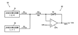
図8に、図1の高次成分発生回路50と高次成分ゲイン調整回路80の詳細な構成例を示す。
4). FIG. 8 shows a detailed configuration example of the high-order
高次成分発生回路50は、出力ノードNIhに接続されるi次成分発生回路51と、ノードNIhに接続されるj次成分発生回路52と、を含む(i,jは、j>i≧4の自然数)。なお、高次成分発生回路50は、ノードNIhに接続されるm次成分発生回路や、ノードNIhに接続されるk次成分発生回路を更に含んでもよい(mは1≦m≦3の自然数、kはk≧4、k≠i,jの自然数)。
High-order
i次成分発生回路51は、i次関数αi(T−T0)iを近似するi次成分電流ISiを出力し、j次成分発生回路52は、j次関数αj(T−T0)jを近似するj次成分電流ISjを出力する。ノードNIhには、これらの電流ISi、ISjが加算された高次成分電流ISh=ISi+ISjが出力され、その高次成分電流IShが高次成分ゲイン調整回路80に入力される。
The i-th order
高次成分ゲイン調整回路80は、負極入力端子がノードNIhに接続され、正極入力端子に図示しない電圧供給回路からの定電圧VRhが供給される演算増幅器OPhと、一端がノードNIhに接続され、他端が出力ノードNVhに接続される可変抵抗素子Rhと、を含む。
The high-order component
高次成分ゲイン調整回路80は、定電圧VRhを基準電圧として高次成分電流IShを電流電圧変換(IV変換)し、高次成分電圧VSh=VRh−Rh×IShを出力する。電流電圧変換のゲイン値はRhであり、このゲイン値Rhが高次成分ゲイン値Ahに対応している。例えば、可変抵抗素子Rhは、直列接続された複数の分割抵抗で構成されており、演算増幅器OPhの負極入力端子に接続される分割タップを、記憶部90に記憶されたゲイン値Ahに基づいて選択し、ゲイン値Rhを設定する。
The high-order component
なお、1次成分ゲイン調整回路60、3次成分ゲイン調整回路70は、上記の高次成分ゲイン調整回路80と同様の構成により実現できるので、図示及び説明を省略する。
Since the primary component gain adjustment circuit 60 and the tertiary component
5.奇数次成分発生回路
図9に、奇数次成分発生回路の詳細な構成例を示す。この構成例は、3次以上の奇数次の成分信号を発生する発生回路に適用できる。即ち、図1の3次成分発生回路40や、図8のi,j次成分発生回路51、52が奇数次成分発生回路である場合や、m次成分発生回路が3次成分発生回路である場合や、k次成分発生回路が奇数次成分発生回路である場合に適用できる。
5. Odd Order Component Generation Circuit FIG. 9 shows a detailed configuration example of the odd order component generation circuit. This configuration example can be applied to a generation circuit that generates odd-order component signals of the third order or higher. That is, the third-order
図9に示すように、奇数次成分発生回路は、温度検出電圧VTを制御電圧VMKに変換する第1の差動回路DF1と、制御電圧VMKを奇数次成分電流ISK(広義には奇数次成分信号)に変換する第2の差動回路DF2と、を含む。 As shown in FIG. 9, the odd-order component generation circuit includes a first differential circuit DF1 that converts the temperature detection voltage VT into a control voltage VMK, and the control voltage VMK as an odd-order component current ISK (in the broad sense, an odd-order component). Signal), a second differential circuit DF2.
第1の差動回路DF1は、図示しない電圧供給回路からの定電圧VR1が一端に供給される抵抗素子R11と、抵抗素子R11の他端にコレクター端子が接続されるバイポーラトランジスターTR1(第1トランジスター)と、バイポーラトランジスターTR1のエミッター端子に一端が接続される抵抗素子R12と、を含む。また、第1の差動回路DF1は、一端に定電圧VR1が供給される抵抗素子R21と、抵抗素子R21の他端にコレクター端子が接続されるバイポーラトランジスターTR2(第2トランジスター)と、バイポーラトランジスターTR2のエミッター端子に一端が接続される抵抗素子R22と、を含む。また、第1の差動回路DF1は、抵抗素子R12の他端及び抵抗素子R22の他端に接続される電流バイアス回路IB1を含む。 The first differential circuit DF1 includes a resistance element R11 to which a constant voltage VR1 from a voltage supply circuit (not shown) is supplied at one end, and a bipolar transistor TR1 (first transistor) having a collector terminal connected to the other end of the resistance element R11. ) And a resistance element R12 having one end connected to the emitter terminal of the bipolar transistor TR1. The first differential circuit DF1 includes a resistive element R21 to which a constant voltage VR1 is supplied at one end, a bipolar transistor TR2 (second transistor) having a collector terminal connected to the other end of the resistive element R21, and a bipolar transistor. And a resistance element R22 having one end connected to the emitter terminal of TR2. The first differential circuit DF1 includes a current bias circuit IB1 connected to the other end of the resistor element R12 and the other end of the resistor element R22.
抵抗素子R11、R21の抵抗値は同一であり、抵抗素子R12、R22の抵抗値は同一であり、バイポーラトランジスターTR1、TR2のサイズは同一である。バイポーラトランジスターTR1のベース端子には、温度検出電圧VTが入力され、バイポーラトランジスターTR2のベース端子には、図示しない電圧供給回路からの所定電圧VR2が入力される。所定電圧VR2は、基準温度T0における温度検出電圧VTと同一の電圧である。これらのバイポーラトランジスターTR1、TR2は、温度検出電圧VTの変化に伴って差動動作を行う。 Resistance elements R11 and R21 have the same resistance value, resistance elements R12 and R22 have the same resistance value, and bipolar transistors TR1 and TR2 have the same size. A temperature detection voltage VT is input to the base terminal of the bipolar transistor TR1, and a predetermined voltage VR2 from a voltage supply circuit (not shown) is input to the base terminal of the bipolar transistor TR2. The predetermined voltage VR2 is the same voltage as the temperature detection voltage VT at the reference temperature T0. These bipolar transistors TR1 and TR2 perform a differential operation as the temperature detection voltage VT changes.
具体的には、バイポーラトランジスターTR1、TR2のコレクター電流をIC1、IC2とし、温度をTとすると、T<T0の温度領域ではVT>VR2となるので、IC1>IC2となる。この温度領域では、図10に示すように、温度Tが下がるほど電圧VMKが上昇し、電圧VR1に漸近していく。一方、T>T0の温度領域ではVT<VR2となるので、IC1<IC2となる。この温度領域では、図10に示すように、温度Tが上がるほど電圧VMKが下降し、電圧VXに漸近していく。電圧VXは、抵抗素子R21、R22の抵抗比で決まる電圧である。図10の例では、VR2=(VR1+VX)/2である。 Specifically, assuming that the collector currents of the bipolar transistors TR1 and TR2 are IC1 and IC2 and the temperature is T, VT> VR2 in the temperature region of T <T0, and therefore IC1> IC2. In this temperature region, as shown in FIG. 10, the voltage VMK increases as the temperature T decreases and gradually approaches the voltage VR1. On the other hand, since VT <VR2 in the temperature range of T> T0, IC1 <IC2. In this temperature region, as shown in FIG. 10, the voltage VMK decreases as the temperature T increases and gradually approaches the voltage VX. The voltage VX is a voltage determined by the resistance ratio of the resistance elements R21 and R22. In the example of FIG. 10, VR2 = (VR1 + VX) / 2.
図11に示すように、基準温度T0(例えば室温)において電圧VMKの傾きと温度検出電圧VTの傾きが同一(ほぼ同一を含む)となるように、バイポーラトランジスターTR1、TR2のサイズや電流バイアス回路IB1の電流値を設定する。このようにすれば、図12(B)で後述するように、基準温度T0付近(例えば室温付近)で奇数次成分電流ISKが変化しなくなるため、奇数次関数(又は図14において偶数次関数)を近似する電流ISKを生成することができる。 As shown in FIG. 11, the size of the bipolar transistors TR1 and TR2 and the current bias circuit so that the slope of the voltage VMK and the slope of the temperature detection voltage VT are the same (including almost the same) at the reference temperature T0 (for example, room temperature). Set the current value of IB1. In this manner, as will be described later with reference to FIG. 12B, the odd-order component current ISK does not change near the reference temperature T0 (for example, near room temperature), so that the odd-order function (or even-order function in FIG. 14). A current ISK that approximates can be generated.
図9の第2の差動回路DF2は、ソース端子が定電圧VR3(例えば電源電圧VDD)のノードに接続されるP型のCMOSトランジスターCM1と、CMOSトランジスターCM1のドレイン端子にコレクター端子が接続されるバイポーラトランジスターTR3(第3トランジスター)と、バイポーラトランジスターTR3のエミッター端子に一端が接続される抵抗素子R3と、を含む。また、第2の差動回路DF2は、ソース端子が定電圧VR3のノードに接続されるP型のCMOSトランジスターCM2と、CMOSトランジスターCM2のドレイン端子にコレクター端子が接続されるバイポーラトランジスターTR4(第4トランジスター)と、バイポーラトランジスターTR4のエミッター端子に一端が接続される抵抗素子R4と、を含む。また、第2の差動回路DF2は、抵抗素子R3の他端及び抵抗素子R3の他端に接続される電流バイアス回路IB2を含む。 The second differential circuit DF2 of FIG. 9 has a P-type CMOS transistor CM1 whose source terminal is connected to a node of a constant voltage VR3 (for example, power supply voltage VDD), and a collector terminal connected to the drain terminal of the CMOS transistor CM1. A bipolar transistor TR3 (third transistor), and a resistance element R3 having one end connected to the emitter terminal of the bipolar transistor TR3. The second differential circuit DF2 includes a P-type CMOS transistor CM2 whose source terminal is connected to the node of the constant voltage VR3, and a bipolar transistor TR4 (fourth transistor) whose collector terminal is connected to the drain terminal of the CMOS transistor CM2. Transistor) and a resistance element R4 having one end connected to the emitter terminal of the bipolar transistor TR4. The second differential circuit DF2 includes a current bias circuit IB2 connected to the other end of the resistance element R3 and the other end of the resistance element R3.
CMOSトランジスターCM1、CM2のサイズは同一であり、カレントミラー回路を構成している。即ち、CM1、CM2のドレイン電流は等しくなる。CM2のドレイン電流は、バイポーラトランジスターTR4のコレクター電流IC4と等しいので、CM1のドレイン電流はID1=IC4である。また、抵抗素子R3、R4の抵抗値は同一であり、バイポーラトランジスターTR3、TR4のサイズは同一である。バイポーラトランジスターTR3のベース端子には制御電圧VMKが入力され、バイポーラトランジスターTR4のベース端子には温度検出電圧VTが入力される。これらのバイポーラトランジスターTR3、TR4は、制御電圧VMK及び温度検出電圧VTの変化に伴って差動動作を行い、TR3のコレクター端子に接続されるノードから奇数次成分電流ISKが出力される。 The CMOS transistors CM1 and CM2 have the same size and form a current mirror circuit. That is, the drain currents of CM1 and CM2 are equal. Since the drain current of CM2 is equal to the collector current IC4 of the bipolar transistor TR4, the drain current of CM1 is ID1 = IC4. The resistance values of the resistance elements R3 and R4 are the same, and the sizes of the bipolar transistors TR3 and TR4 are the same. The control voltage VMK is input to the base terminal of the bipolar transistor TR3, and the temperature detection voltage VT is input to the base terminal of the bipolar transistor TR4. These bipolar transistors TR3 and TR4 perform a differential operation in accordance with changes in the control voltage VMK and the temperature detection voltage VT, and an odd-order component current ISK is output from a node connected to the collector terminal of TR3.
TR3、TR4の差動動作について、図12(A)に示す制御電圧VMKa及び図12(B)に示す奇数次成分電流ISKaを例にとって説明する。図11で説明したように、基準温度T0付近ではVMKa=VTである。そのため、図9に示すように、バイポーラトランジスターTR3、TR4のコレクター電流をIC3、IC4とすると、VMKa=VTである温度範囲ではIC3=IC4となる。CMOSトランジスターCM1のドレイン電流はID1=IC4であるため、ISKa=ID1−IC3=IC4−IC3=0となる。即ち、図12(B)に示すように、VMKa=VTである温度範囲をTLKa<T<THKaとすると、この温度範囲ではISKa=0である。 The differential operation of TR3 and TR4 will be described taking the control voltage VMKa shown in FIG. 12A and the odd-order component current ISKa shown in FIG. 12B as examples. As described with reference to FIG. 11, VMKa = VT in the vicinity of the reference temperature T0. Therefore, as shown in FIG. 9, when the collector currents of the bipolar transistors TR3 and TR4 are IC3 and IC4, IC3 = IC4 in the temperature range where VMKa = VT. Since the drain current of the CMOS transistor CM1 is ID1 = IC4, ISKa = ID1-IC3 = IC4-IC3 = 0. That is, as shown in FIG. 12B, if the temperature range where VMKa = VT is TLKa <T <THKa, ISKa = 0 in this temperature range.
T<TLKaの温度範囲ではVMKa<VTであるため、IC3<IC4となり、ISKa=IC4−IC3>0となる。図12(B)に示すように、T<TLKaの温度範囲では温度Tが下がるほどISKaは大きくなり、ISKaは負の傾きを有している。一方、T>TLKaの温度範囲では、VMKa>VTであるため、IC3>IC4となり、ISKa=IC4−IC3<0となる。図12(B)に示すように、T>TLKaの温度範囲では温度Tが上がるほどISKaは大きくなり、ISKaは負の傾きを有している。 Since VMKa <VT in the temperature range of T <TLKa, IC3 <IC4 and ISKa = IC4-IC3> 0. As shown in FIG. 12B, in the temperature range of T <TLKa, ISKa increases as the temperature T decreases, and ISKa has a negative slope. On the other hand, in the temperature range of T> TLKa, since VMKa> VT, IC3> IC4 and ISKa = IC4-IC3 <0. As shown in FIG. 12B, in the temperature range of T> TLKa, ISKa increases as the temperature T increases, and ISKa has a negative slope.
奇数次関数の次数は、図12(A)に示すように、電圧範囲(VR1−VX)を調整することで決定され、電圧範囲(VR1−VX)が小さいほど次数が小さくなる。例えば、図12(A)に示す制御電圧VMKa〜VMKcの電圧範囲は、(VR1a−VXa)>(VR1b−VXb)>(VR1c−VXc)である。図12(B)に示すように、奇数次成分電流がISKa〜ISKc=0となる温度範囲は、制御電圧VMKa〜VMKcの電圧範囲に応じて、(THKa−TLKa)>(THKb−TLKb)>(THKc−TLKc)である。ISK=0である温度範囲(THK−TLK)が広いほど高次数の関数を近似しており、例えばISKa、ISKb、ISKcは、7次、5次、3次成分電流である。 As shown in FIG. 12A, the order of the odd-order function is determined by adjusting the voltage range (VR1-VX), and the order decreases as the voltage range (VR1-VX) decreases. For example, the voltage range of the control voltages VMKa to VMKc shown in FIG. 12A is (VR1a-VXa)> (VR1b-VXb)> (VR1c-VXc). As shown in FIG. 12B, the temperature range in which the odd-order component current is ISKa to ISKc = 0 is (THKa−TLKa)> (THKb−TLKb)> according to the voltage range of the control voltages VMKa to VMKc> (THKc-TLKc). As the temperature range (THK-TLK) where ISK = 0 is wider, higher order functions are approximated. For example, ISKa, ISKb, and ISKc are seventh, fifth, and third order component currents.
図13に、奇数次成分電流ISKを、図8で説明した高次成分ゲイン調整回路80により電流電圧変換した場合の、奇数次成分電圧VSKの特性例を示す。図8で説明したように、奇数次成分電圧は、VSK=VRh−Rh×ISKとなる。これは反転増幅であるため、図13に示すVSKの傾きと、図12(B)に示すISKの傾きは、符号が反転されている。このようにして、基準温度T0を含む温度範囲TLK<T0<THKにおいて一定の電圧であり、温度範囲T<TLK、THK<Tにおいて正の傾きをもつ奇数次成分電圧VSKを得ることができる。
FIG. 13 shows a characteristic example of the odd-order component voltage VSK when the odd-order component current ISK is subjected to current-voltage conversion by the high-order component
なお、本実施形態はこれに限定されず、温度範囲T<TLK、THK<Tにおいて負の傾きをもつ奇数次成分電圧VSKが得られるように奇数次成分発生回路やゲイン調整回路を構成してもよい。 The present embodiment is not limited to this, and an odd-order component generation circuit and a gain adjustment circuit are configured so that an odd-order component voltage VSK having a negative slope in the temperature ranges T <TLK and THK <T can be obtained. Also good.
6.偶数次成分発生回路
図14に、偶数次成分発生回路の詳細な構成例を示す。この構成例は、2次以上の偶数次の成分信号を発生する発生回路に適用できる。即ち、図8のi,j次成分発生回路51、52が偶数次成分発生回路である場合や、m次成分発生回路が2次成分発生回路である場合や、k次成分発生回路が偶数次成分発生回路である場合に適用できる。
6). FIG. 14 shows a detailed configuration example of the even-order component generation circuit. This configuration example can be applied to a generation circuit that generates second-order or higher-order component signals. That is, the i-th and j-th order
図14に示すように、偶数次成分発生回路は、温度検出電圧VTを制御電圧VMGに変換する第3の差動回路DF3と、制御電圧VMGを差動電流IC7、IC8に変換する第4の差動回路DF4と、差動電流IC7、IC8に基づいて偶数次成分電流ISG(広義には偶数次成分信号)を出力する出力回路ISQと、を含む。 As shown in FIG. 14, the even-order component generation circuit includes a third differential circuit DF3 that converts the temperature detection voltage VT into a control voltage VMG, and a fourth differential circuit that converts the control voltage VMG into differential currents IC7 and IC8. A differential circuit DF4 and an output circuit ISQ that outputs an even-order component current ISG (even-order component signal in a broad sense) based on the differential currents IC7 and IC8 are included.
第3の差動回路DF3は、抵抗素子R51、R52、バイポーラトランジスターTR5(第5トランジスター)、抵抗素子R61、R62、バイポーラトランジスターTR6(第6トランジスター)、電流バイアス回路IB3を含む。第3の差動回路DF3は、図9で説明した第1の差動回路DF1と同様の構成及び動作であるため、説明を省略する。 The third differential circuit DF3 includes resistance elements R51 and R52, a bipolar transistor TR5 (fifth transistor), resistance elements R61 and R62, a bipolar transistor TR6 (sixth transistor), and a current bias circuit IB3. The third differential circuit DF3 has the same configuration and operation as the first differential circuit DF1 described in FIG.
なお本実施形態では、3次成分発生回路40、i次成分発生回路51、j次成分発生回路52、m次成分発生回路、k次成分発生回路に対して、それぞれ差動回路DF1(又はDF3)を設けてもよいし、共通の1つの差動回路DF1を設けてもよい。
In the present embodiment, the differential circuit DF1 (or DF3) is applied to the third order
第4の差動回路DF4は、P型のCMOSトランジスターCM3、抵抗素子R7、バイポーラトランジスターTR7(第7トランジスター)、P型のCMOSトランジスターCM4、抵抗素子R8、バイポーラトランジスターTR8(第8トランジスター)、電流バイアス回路IB4を含む。第4の差動回路DF4は、図9で説明した第2の差動回路DF2と同様の構成及び動作であるため、説明を省略する。 The fourth differential circuit DF4 includes a P-type CMOS transistor CM3, a resistor element R7, a bipolar transistor TR7 (seventh transistor), a P-type CMOS transistor CM4, a resistor element R8, a bipolar transistor TR8 (eighth transistor), a current A bias circuit IB4 is included. The fourth differential circuit DF4 has the same configuration and operation as the second differential circuit DF2 described in FIG.
出力回路ISQは、ソース端子が定電圧VR3(例えば電源電圧VDD)のノードに接続されるP型のCMOSトランジスターCM5〜CM7を含む。また、出力回路ISQは、コレクター端子がCMOSトランジスターCM6、CM7のドレイン端子に接続されるバイポーラトランジスターTR9と、グランド電圧VSSのノードに一端が接続され、他端がバイポーラトランジスターTR9のエミッター端子に接続される抵抗素子R9と、グランド電圧VSSのノードに一端が接続される抵抗素子R10と、エミッター端子が抵抗素子R10の他端に接続されるバイポーラトランジスターTR10と、を含む。また、出力回路ISQは、CMOSトランジスターCM6のドレイン端子及びCMOSトランジスターCM7のドレイン端子に接続される電流バイアス回路IB5を含む。 Output circuit ISQ includes P-type CMOS transistors CM5 to CM7 whose source terminals are connected to a node of constant voltage VR3 (for example, power supply voltage VDD). The output circuit ISQ has a collector terminal connected to the drain terminals of the CMOS transistors CM6 and CM7, one end connected to the node of the ground voltage VSS, and the other end connected to the emitter terminal of the bipolar transistor TR9. Resistor element R9, a resistor element R10 having one end connected to the node of the ground voltage VSS, and a bipolar transistor TR10 having an emitter terminal connected to the other end of the resistor element R10. The output circuit ISQ includes a current bias circuit IB5 connected to the drain terminal of the CMOS transistor CM6 and the drain terminal of the CMOS transistor CM7.
CMOSトランジスターCM5のドレイン端子は、バイポーラトランジスターTR7のコレクター端子のノードに接続され、CMOSトランジスターCM5、CM6はカレントミラー回路を構成している。CM5のドレイン電流IH’は、図9の電流ISKと比較するとIH’=−ISKなので、図12(B)から、T<T0の温度範囲においてIH’≦0である。IH’≦0の場合はミラーされないので、T<T0の温度範囲では、CM6のドレイン電流はIHa=0である。一方、T>T0の温度範囲ではIH’=−ISK≧0なので、CM5、CM6のサイズが同一である場合を例にとると、IHa=−ISKとなる。以上より、IHaは図16に示すような特性となる。 The drain terminal of the CMOS transistor CM5 is connected to the node of the collector terminal of the bipolar transistor TR7, and the CMOS transistors CM5 and CM6 constitute a current mirror circuit. Since the drain current IH ′ of CM5 is IH ′ = − ISK as compared with the current ISK of FIG. 9, from FIG. 12B, IH ′ ≦ 0 in the temperature range of T <T0. Since mirroring is not performed when IH ′ ≦ 0, the drain current of CM6 is IHa = 0 in the temperature range of T <T0. On the other hand, since IH ′ = − ISK ≧ 0 in the temperature range of T> T0, when the sizes of CM5 and CM6 are the same, IHa = −ISK. From the above, IHa has characteristics as shown in FIG.
一方、CMOSトランジスターCM7は、CMOSトランジスターCM4とカレントミラー回路を構成している。即ち、CM4、CM7のサイズが同一である場合を例にとると、CM7のドレイン電流ILaはCM4のドレイン電流IC8と同一(ILa=IC8)である。IC8+IC7=IB4、IC8=IC7−IH’、IH’=−ISKより、ILa=IC8=IB4×0.5−ISK×0.5となり、ILaは図15に示すような特性となる。電流バイアス回路IB5は、バイアス電流IB5=IB4×0.5を発生するので、ILa−IB5=ISK×0.5となり、ILa−IB5は図16に示すような特性となる。 On the other hand, the CMOS transistor CM7 constitutes a current mirror circuit with the CMOS transistor CM4. That is, taking the case where the sizes of CM4 and CM7 are the same as an example, the drain current ILa of CM7 is the same as the drain current IC8 of CM4 (ILa = IC8). From IC8 + IC7 = IB4, IC8 = IC7−IH ′, IH ′ = − ISK, ILa = IC8 = IB4 × 0.5−ISK × 0.5, and ILa has characteristics as shown in FIG. Since the current bias circuit IB5 generates the bias current IB5 = IB4 × 0.5, ILa−IB5 = ISK × 0.5, and ILa-IB5 has characteristics as shown in FIG.
以上より、T<T0の温度範囲ではIHa=0、ILa−IB5=ISK×0.5なので、ISG’=IHa+(ILa−IB5)=ISK×0.5となる。T>T0の温度範囲ではIHa=−ISK、ILa−IB5=ISK×0.5なので、ISG’=−ISK×0.5となる。即ち、図17に示すように、電流ISG’は、温度T0に対して線対称な電流となる。バイポーラトランジスターTR9、TR10のサイズが同一である場合を例にとると、ISG=ISG’であり、基準温度T0に対して線対称な偶数次成分信号ISGを得ることができる。 From the above, in the temperature range of T <T0, IHa = 0 and ILa−IB5 = ISK × 0.5, so ISG ′ = IHa + (ILa−IB5) = ISK × 0.5. In the temperature range of T> T0, since IHa = −ISK and ILa−IB5 = ISK × 0.5, ISG ′ = − ISK × 0.5. That is, as shown in FIG. 17, the current ISG ′ is a current that is line-symmetric with respect to the temperature T0. Taking the case where the bipolar transistors TR9 and TR10 have the same size as an example, ISG = ISG ', and an even-order component signal ISG that is line-symmetric with respect to the reference temperature T0 can be obtained.
偶数次関数の次数は、奇数次関数と同様に、制御信号VMGの電圧範囲(VR1−VX)を調整することで決定され、電圧範囲(VR1−VX)が小さいほど次数が小さくなる。即ち、図18に示すように、偶数次成分電流がISGa〜ISGc=0となる温度範囲は、図12(A)に示す制御電圧VMKa〜VMKc(VMGa〜VMGc)の電圧範囲に応じて、(THGa−TLGa)>(THGb−TLGb)>(THGc−TLGc)である。ISG=0である温度範囲(THG−TLG)が広いほど高次数の関数を近似しており、例えばISGa、ISGb、ISGcは、6次、4次、2次成分電流である。 Similar to the odd-order function, the order of the even-order function is determined by adjusting the voltage range (VR1-VX) of the control signal VMG, and the order decreases as the voltage range (VR1-VX) decreases. That is, as shown in FIG. 18, the temperature range in which the even-order component current becomes ISGa to ISGc = 0 is in accordance with the voltage range of the control voltages VMKa to VMKc (VMGa to VMGc) shown in FIG. THGa-TLGa)> (THGb-TLGb)> (THGc-TLGc). As the temperature range (THG-TLG) where ISG = 0 is wider, higher order functions are approximated. For example, ISGa, ISGb, and ISGc are sixth-order, fourth-order, and second-order component currents.
図19に、偶数次成分電流ISGを、図8で説明した高次成分ゲイン調整回路80により電流電圧変換した場合の、偶数次成分電圧VSGの特性例を示す。図8で説明したように、偶数次成分電圧は、VSG=VRh+Rh×ISG(ISGとIShは電流の向きの定義が逆)となる。これは正転増幅であるため、図18に示すVSGの傾きと、図18に示すISGの傾きは、符号が同一である。このようにして、基準温度T0を含む温度範囲TLG<T0<THGにおいて一定の電圧であり、温度範囲T<TLGにおいて負の傾きをもち、THG<Tにおいて正の傾きをもつ偶数次成分電圧VSGを得ることができる。
FIG. 19 shows a characteristic example of the even-order component voltage VSG when the even-order component current ISG is converted into a current-voltage by the high-order component
なお、本実施形態はこれに限定されず、温度範囲T<TLGにおいて正の傾きをもち、THG<Tにおいて負の傾きをもつ偶数次成分電圧VSGが得られるように偶数次成分発生回路やゲイン調整回路を構成してもよい。 The present embodiment is not limited to this, and an even-order component generation circuit and a gain are provided so that an even-order component voltage VSG having a positive slope in the temperature range T <TLG and a negative slope in THG <T can be obtained. An adjustment circuit may be configured.
7.発振回路
図20に、本実施形態の温度補償回路を適用できる発振回路の構成例を示す。
7). Oscillation Circuit FIG. 20 shows a configuration example of an oscillation circuit to which the temperature compensation circuit of this embodiment can be applied.
図20の発振回路は、エミッター端子がグランド電圧VSSのノードに接続されるバイポーラトランジスターTRXと、一端がバイポーラトランジスターTRXのベース端子に接続され、他端がバイポーラトランジスターTRXのコレクター端子に接続される抵抗素子RXと、バイポーラトランジスターTRXのコレクター端子にバイアス電流を供給する電流バイアス回路IBXと、を含む。また、発振回路は、一端がバイポーラトランジスターTRXのコレクター端子に接続されるキャパシターC3と、一端がキャパシターC3の他端に接続され、他端がバイポーラトランジスターTRXのベース端子に接続される水晶振動子XTALと、を含む。また、発振回路は、一端が水晶振動子XTALの一端に接続され、他端がグランド電圧VSSのノードに接続される可変容量キャパシターC1と、一端が水晶振動子XTALの他端に接続され、他端がグランド電圧VSSのノードに接続されるキャパシターC2と、を含む。 The oscillation circuit of FIG. 20 includes a bipolar transistor TRX whose emitter terminal is connected to the node of the ground voltage VSS, a resistor whose one end is connected to the base terminal of the bipolar transistor TRX, and the other end connected to the collector terminal of the bipolar transistor TRX. The device includes an element RX and a current bias circuit IBX that supplies a bias current to the collector terminal of the bipolar transistor TRX. The oscillation circuit includes a capacitor C3 having one end connected to the collector terminal of the bipolar transistor TRX, and a crystal resonator XTAL having one end connected to the other end of the capacitor C3 and the other end connected to the base terminal of the bipolar transistor TRX. And including. The oscillation circuit has one end connected to one end of the crystal resonator XTAL, the other end connected to the node of the ground voltage VSS, one end connected to the other end of the crystal resonator XTAL, and the other. A capacitor C2 having an end connected to the node of the ground voltage VSS.
バイポーラトランジスターTRXには、水晶振動子XTALの発振により生じたベース−エミッター間電流が流れる。ベース−エミッター間電流が増加すると、コレクター−エミッター間電流が増加し、電流バイアス回路IBXから抵抗素子RXに分岐するバイアス電流が減少するので、コレクター電圧Vcが低下する。一方、ベース−エミッター間電流が減少すると、コレクター−エミッター間電流が減少し、電流バイアス回路IBXから抵抗素子RXに分岐するバイアス電流が増加するので、コレクター電圧Vcが上昇する。コレクター電圧VcはキャパシターC3を介して水晶振動子XTALにフィードバックされるので、水晶振動子XTALが発振する。 A current between the base and the emitter generated by the oscillation of the crystal unit XTAL flows through the bipolar transistor TRX. When the base-emitter current increases, the collector-emitter current increases, and the bias current branching from the current bias circuit IBX to the resistance element RX decreases, so the collector voltage Vc decreases. On the other hand, when the base-emitter current decreases, the collector-emitter current decreases, and the bias current branched from the current bias circuit IBX to the resistance element RX increases, so that the collector voltage Vc increases. Since the collector voltage Vc is fed back to the crystal resonator XTAL via the capacitor C3, the crystal resonator XTAL oscillates.
水晶振動子XTALの発振周波数は温度特性(例えば図2の温度特性)をもっており、その温度特性は、温度補償回路が発生した温度補償用電圧VCOMPにより補償される。即ち、温度補償用電圧VCOMPは可変容量キャパシターC1に入力され、その温度補償用電圧VCOMPにより可変容量キャパシターC1の容量値が制御される。可変容量キャパシターC1の容量値が変化すると発振ループの共振周波数が変化するので、水晶振動子XTALの温度特性による発振周波数の変動が補償される。可変容量キャパシターC1は、例えば可変容量ダイオード(バラクター)により構成される。 The oscillation frequency of the crystal resonator XTAL has a temperature characteristic (for example, the temperature characteristic of FIG. 2), and the temperature characteristic is compensated by the temperature compensation voltage VCOMP generated by the temperature compensation circuit. That is, the temperature compensation voltage VCOMP is input to the variable capacitor C1, and the capacitance value of the variable capacitor C1 is controlled by the temperature compensation voltage VCOMP. When the capacitance value of the variable capacitor C1 changes, the resonance frequency of the oscillation loop changes, so that fluctuations in the oscillation frequency due to the temperature characteristics of the crystal resonator XTAL are compensated. The variable capacitance capacitor C1 is configured by, for example, a variable capacitance diode (varactor).
なお、本実施形態の発振回路は図20の構成に限定されず、種々の発振回路を採用することが可能である。また、図20ではC1を可変容量キャパシターとする場合を例に説明したが、本実施形態はこれに限定されず、C2又はC3を、VCOMPで制御される可変容量キャパシターとしてもよい。また、C1〜C3のうち複数を、VCOMPで制御される可変容量キャパシターとしてもよい。 Note that the oscillation circuit of the present embodiment is not limited to the configuration of FIG. 20, and various oscillation circuits can be employed. In FIG. 20, the case where C1 is a variable capacitor has been described as an example. However, the present embodiment is not limited to this, and C2 or C3 may be a variable capacitor controlled by VCOMP. A plurality of C1 to C3 may be variable capacitors controlled by VCOMP.
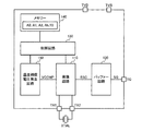
8.回路装置
図21に、本実施形態の温度補償回路を適用できる回路装置の構成例を示す。
8). Circuit Device FIG. 21 shows a configuration example of a circuit device to which the temperature compensation circuit of this embodiment can be applied.
図21の発振回路装置は、発振回路110、バッファー回路120、制御回路130、メモリー140(記憶部)、温度補償電圧発生回路150(温度補償回路)を含む。なお回路装置の構成は図1の構成には限定されず、その一部の構成要素を省略したり、他の構成要素を追加するなどの種々の変形実施が可能である。
The oscillation circuit device of FIG. 21 includes an
発振回路110は、振動子XTAL(圧電振動子、水晶振動子)に接続される。具体的には第1、第2の振動子用端子TX1、TX2(振動子用パッド)を介して振動子XTALに接続される。発振回路110は、電圧を印加することで固有振動を起こす振動子XTALを一定の周波数で発振させるための回路である。この発振回路110は、端子TX1が入力ノードに接続され、端子TX2が出力ノードに接続される増幅回路などにより実現できる。
The
バッファー回路120は、発振回路110からの発振信号SSCをバッファリングする回路である。即ち外部の負荷を十分に駆動できるように信号のバッファリングを行う。バッファー回路120により、バッファリングされた信号は、出力信号SQとして出力端子TQを介して外部に出力される。
The
制御回路130は、発振回路110、バッファー回路120、メモリー140、温度補償電圧発生回路150の制御を行う。また外部とのインターフェース処理なども行う。この制御回路130は、例えばスタンダードセルやゲートアレイ等のロジック回路により実現される。
The
メモリー140は、回路装置の動作に必要な各種の情報を記憶する。例えば温度補償電圧発生回路150が温度補償処理を行うために必要な情報(ゲイン値A0、A1、A3、Ah、基準温度T0)等を記憶する。この情報は、電源端子TVD、TVS、出力端子TQ、振動子用端子TX1、TX2、及び制御回路130を介して外部から書き込まれる。
The
温度補償電圧発生回路150は、TCXOを実現するための温度補償用電圧を発生して、発振回路110に出力する。これにより発振周波数の温度補償が実現される。
The temperature compensation
9.電子機器
図22に本実施形態の回路装置を含む電子機器の構成例を示す。この電子機器は、本実施形態の回路装置500、水晶振動子等の振動子XTAL、アンテナANT、通信部510、処理部520を含む。また操作部530、表示部540、メモリー550(記憶部)を含むことができる。なおこれらの一部の構成要素を省略したり、他の構成要素を追加するなどの種々の変形実施が可能である。
9. Electronic Device FIG. 22 shows a configuration example of an electronic device including the circuit device of this embodiment. The electronic apparatus includes the
図22の電子機器としては、例えば携帯型情報端末(携帯電話、スマートフォーン)、生体計測機器(脈拍計、歩数計等)、映像機器(デジタルカメラ、ビデオカメラ)などの種々の機器を想定できる。 As the electronic device in FIG. 22, various devices such as a portable information terminal (mobile phone, smart phone), a biological measurement device (pulse meter, pedometer, etc.), and a video device (digital camera, video camera) can be assumed. .
通信部510(無線回路)は、アンテナANTを介して外部からデータを受信したり、外部にデータを送信する処理を行う。処理部520は、電子機器の制御処理や、通信部510を介して送受信されるデータの種々のデジタル処理などを行う。この処理部520の機能は、例えばマイクロコンピューターなどのプロセッサーにより実現される。
The communication unit 510 (wireless circuit) performs processing of receiving data from the outside via the antenna ANT and transmitting data to the outside. The
操作部530は、ユーザーが入力操作を行うためのものであり、操作ボタンやタッチパネルディスプレイをなどにより実現できる。表示部540は、各種の情報を表示するものであり、液晶や有機ELなどのディスプレイにより実現できる。なお操作部530としてタッチパネルディスプレイを用いる場合には、このタッチパネルディスプレイが表示部540の機能を兼ねることになる。記憶部550は、データを記憶するものであり、その機能はRAMやROMなどの半導体メモリーやHDD(ハードディスクドライブ)などにより実現できる。
The
なお、上記のように本実施形態について詳細に説明したが、本発明の新規事項および効果から実体的に逸脱しない多くの変形が可能であることは当業者には容易に理解できるであろう。従って、このような変形例はすべて本発明の範囲に含まれるものとする。例えば、明細書又は図面において、少なくとも一度、より広義又は同義な異なる用語と共に記載された用語は、明細書又は図面のいかなる箇所においても、その異なる用語に置き換えることができる。また本実施形態及び変形例の全ての組み合わせも、本発明の範囲に含まれる。また温度補償回路、回路装置、電子機器等の構成・動作や、温度補償用電圧の調整方法等も本実施形態で説明したものに限定に限定されず、種々の変形実施が可能である。 Although the present embodiment has been described in detail as described above, it will be easily understood by those skilled in the art that many modifications can be made without departing from the novel matters and effects of the present invention. Accordingly, all such modifications are intended to be included in the scope of the present invention. For example, a term described with a different term having a broader meaning or the same meaning at least once in the specification or the drawings can be replaced with the different term in any part of the specification or the drawings. All combinations of the present embodiment and the modified examples are also included in the scope of the present invention. The configuration and operation of the temperature compensation circuit, circuit device, electronic device, etc., the method for adjusting the temperature compensation voltage, and the like are not limited to those described in this embodiment, and various modifications can be made.
10 温度センサー、15 基準温度調整回路、20 0次成分発生回路、
30 1次成分発生回路、40 3次成分発生回路、50 高次成分発生回路、
51 i次成分発生回路、52 j次成分発生回路、60 1次成分ゲイン調整回路、
70 3次成分ゲイン調整回路、80 高次成分ゲイン調整回路、90 記憶部、
100 加算回路、110 発振回路、120 バッファー回路、130 制御回路、
140 メモリー、150 温度補償電圧発生回路、500 回路装置、
510 通信部、520 処理部、530 操作部、540 表示部、
550 メモリー、
A0,A1,A3,Ah ゲイン値、ANT アンテナ、
C1 可変容量キャパシター、C2,C3 キャパシター、
CM1〜CM7 CMOSトランジスター、DF1〜DF4 第1〜第4の差動回路、
IB1〜IB4,IBX 電流バイアス回路、IS1 1次成分電流、
IS3 3次成分電流、ISG 偶数次成分電流、ISh 高次成分電流、
ISi i次成分電流、ISj j次成分電流、ISK 奇数次成分電流、
ISQ 出力回路、OPA,OPh 演算増幅器、R10 抵抗素子、
R11,R12,R21,R22,R3,R4 抵抗素子、
R51,R52,R61,R62,R7,R8 抵抗素子、
RA1,RA2 抵抗素子、Rh 可変抵抗素子、RT,RX 抵抗素子、
SQ 出力信号、SSC 発振信号、T 温度、T0 基準温度、TQ 出力端子、
TR1〜TR8 バイポーラトランジスター(第1〜第8トランジスター)、
TR9,TR10 バイポーラトランジスター、
TRT1,TRT2,TRX バイポーラトランジスター、
TVD,TVS 電源端子、TX1 振動子用端子、VAT0 基準電圧、
Vc コレクター電圧、VCOMP 温度補償用電圧、VDD 電源電圧、
VMG,VMK 制御電圧、VR1,VR3,VRh,VRT 定電圧、
VR2 所定電圧、VS0 0次成分電圧、VS1 1次成分電圧、
VS3 3次成分電圧、VSG 偶数次成分電圧、VSh 高次成分電圧、
VSK 奇数次成分電圧、VSS グランド電圧、VT 温度検出電圧、
XTAL 水晶振動子
10 temperature sensor, 15 reference temperature adjustment circuit, 20th order component generation circuit,
30 primary component generation circuit, 40 tertiary component generation circuit, 50 higher order component generation circuit,
51 i-order component generation circuit, 52 j-order component generation circuit, 60 primary component gain adjustment circuit,
70 third-order component gain adjustment circuit, 80 higher-order component gain adjustment circuit, 90 storage unit,
100 addition circuit, 110 oscillation circuit, 120 buffer circuit, 130 control circuit,
140 memory, 150 temperature compensation voltage generation circuit, 500 circuit device,
510 communication unit, 520 processing unit, 530 operation unit, 540 display unit,
550 memory,
A0, A1, A3, Ah gain value, ANT antenna,
C1 variable capacitor, C2, C3 capacitor,
CM1 to CM7 CMOS transistors, DF1 to DF4, first to fourth differential circuits,
IB1 to IB4, IBX current bias circuit, IS1 primary component current,
IS3 Third-order component current, ISG even-order component current, ISh higher-order component current,
ISi i-order component current, ISj j-order component current, ISK odd-order component current,
ISQ output circuit, OPA, OPh operational amplifier, R10 resistance element,
R11, R12, R21, R22, R3, R4 resistance elements,
R51, R52, R61, R62, R7, R8 resistance elements,
RA1, RA2 resistance elements, Rh variable resistance elements, RT, RX resistance elements,
SQ output signal, SSC oscillation signal, T temperature, T0 reference temperature, TQ output terminal,
TR1 to TR8 bipolar transistors (first to eighth transistors),
TR9, TR10 bipolar transistors,
TRT1, TRT2, TRX bipolar transistors,
TVD, TVS power supply terminal, TX1 vibrator terminal, VAT0 reference voltage,
Vc collector voltage, VCOMP temperature compensation voltage, VDD power supply voltage,
VMG, VMK control voltage, VR1, VR3, VRh, VRT constant voltage,
VR2 predetermined voltage, VS0 zero order component voltage, VS1 primary component voltage,
VS3 third-order component voltage, VSG even-order component voltage, VSh higher-order component voltage,
VSK odd-order component voltage, VSS ground voltage, VT temperature detection voltage,
XTAL crystal unit
Claims (15)
前記検出信号に基づいて、前記温度に対して3次関数で近似された3次成分信号を出力する3次成分発生回路と、
前記検出信号に基づいて、前記温度に対して高次関数で近似された高次成分信号を出力する高次成分発生回路と、
前記1次成分信号が入力され、前記1次成分信号のゲインを調整して1次出力信号を出力する1次成分ゲイン調整回路と、
前記3次成分信号が入力され、前記3次成分信号のゲインを調整して3次出力信号を出力する3次成分ゲイン調整回路と、
前記高次成分信号が入力され、前記高次成分信号のゲインを調整して高次出力信号を出力する高次成分ゲイン調整回路と、
前記1次出力信号と前記3次出力信号と前記高次出力信号とを加算して温度補償用電圧として出力する加算回路と、
を含み、
前記高次成分発生回路は、
3次関数よりも高次のi次関数(iは4以上の自然数)で近似された信号と、前記i次関数よりも高次のj次関数(jはj>iの自然数)で近似された信号と、が少なくとも合成された信号を、前記高次成分信号として出力し、
前記温度補償電圧をVCOMPとし、
前記1次成分ゲイン調整回路のゲイン値をA1とし、前記3次成分ゲイン調整回路のゲイン値をA3とし、前記高次成分ゲイン調整回路のゲイン値をAhとし、温度をTとし、基準温度をT0とし、αi、αjを所定の係数とし、f(T−T0)を温度Tの関数として、
VCOMP=Ah×(αi×(T−T0) i +αj×(T−T0) j +
f(T−T0))+A3×(T−T0) 3 +A1×(T−T0)+A0
の関係を満足することを特徴とする温度補償回路。 A primary component generation circuit that outputs a primary component signal approximated by a linear function with respect to temperature based on a detection signal from a temperature sensor;
A third-order component generation circuit that outputs a third-order component signal approximated by a third-order function with respect to the temperature based on the detection signal;
A high-order component generation circuit that outputs a high-order component signal approximated by a high-order function with respect to the temperature based on the detection signal;
A primary component gain adjustment circuit that receives the primary component signal, adjusts the gain of the primary component signal, and outputs a primary output signal;
A third-order component gain adjustment circuit that receives the third-order component signal, adjusts the gain of the third-order component signal, and outputs a third-order output signal;
A high-order component gain adjustment circuit that receives the high-order component signal, adjusts the gain of the high-order component signal, and outputs a high-order output signal;
An adding circuit for adding the primary output signal, the tertiary output signal, and the high-order output signal to output as a temperature compensation voltage;
Including
The higher-order component generation circuit includes:
It is approximated by a signal approximated by a higher-order i-th order function (i is a natural number of 4 or more) than a cubic function and a higher-order j-th order function (j is a natural number where j> i). And at least the synthesized signal is output as the higher-order component signal ,
The temperature compensation voltage is VCOMP,
The gain value of the first-order component gain adjustment circuit is A1, the gain value of the third-order component gain adjustment circuit is A3, the gain value of the higher-order component gain adjustment circuit is Ah, the temperature is T, and the reference temperature is T0, αi and αj are predetermined coefficients, and f (T−T0) is a function of temperature T.
VCOMP = Ah × (αi × (T−T0) i + αj × (T−T0) j +
f (T−T0)) + A3 × (T−T0) 3 + A1 × (T−T0) + A0
A temperature compensation circuit characterized by satisfying the relationship:
前記高次成分発生回路は、
前記i次関数と、前記j次関数と、1次以上3次以下の関数であるm次関数(mは1≦m≦3の自然数)とで近似された信号が合成された信号を、前記高次成分信号として出力することを特徴とする温度補償回路。 In claim 1,
The higher-order component generation circuit includes:
A signal obtained by synthesizing a signal approximated by the i-order function, the j-order function, and an m-order function (m is a natural number satisfying 1 ≦ m ≦ 3), which is a function of 1st order to 3rd order, A temperature compensation circuit which outputs as a high-order component signal.
前記高次成分発生回路は、
前記i次関数と、前記j次関数と、前記j次関数よりも高次のk次関数(kはk>jの自然数)とで近似された信号が合成された信号を、前記高次成分信号として出力することを特徴とする温度補償回路。 In claim 1,
The higher-order component generation circuit includes:
A signal obtained by synthesizing a signal approximated by the i-order function, the j-order function, and a k-order function higher than the j-order function (k is a natural number of k> j) is expressed as the higher-order component. A temperature compensation circuit which outputs as a signal.
mを1≦m≦3の自然数とし、αmを所定の係数として、
f(T−T0)=αm×(T−T0)m
であることを特徴とする温度補償回路。 In claim 1 ,
m is a natural number of 1 ≦ m ≦ 3, αm is a predetermined coefficient,
f (T−T0) = αm × (T−T0) m
A temperature compensation circuit characterized by the above.
kをk>j>i≧4の自然数とし、αkを所定の係数として、
f(T−T0)=αk×(T−T0)k
であることを特徴とする温度補償回路。 In claim 1 ,
k is a natural number of k>j> i ≧ 4, αk is a predetermined coefficient,
f (T−T0) = αk × (T−T0) k
A temperature compensation circuit characterized by the above.
前記検出信号に基づいて、前記温度に対して3次関数で近似された3次成分信号を出力する3次成分発生回路と、
前記検出信号に基づいて、前記温度に対して高次関数で近似された高次成分信号を出力する高次成分発生回路と、
前記1次成分信号が入力され、前記1次成分信号のゲインを調整して1次出力信号を出力する1次成分ゲイン調整回路と、
前記3次成分信号が入力され、前記3次成分信号のゲインを調整して3次出力信号を出力する3次成分ゲイン調整回路と、
前記高次成分信号が入力され、前記高次成分信号のゲインを調整して高次出力信号を出力する高次成分ゲイン調整回路と、
前記1次出力信号と前記3次出力信号と前記高次出力信号とを加算して温度補償用電圧として出力する加算回路と、
を含み、
前記高次成分発生回路は、
3次関数よりも高次のi次関数(iは4以上の自然数)で近似された信号と、前記i次関数よりも高次のj次関数(jはj>iの自然数)で近似された信号と、が少なくとも合成された信号を、前記高次成分信号として出力し、
前記温度補償電圧をVCOMPとし、
前記1次成分ゲイン調整回路のゲイン値をA1とし、前記3次成分ゲイン調整回路のゲイン値をA3とし、前記高次成分ゲイン調整回路のゲイン値をAhとし、温度をTとし、基準温度をT0とし、αi、αjを所定の係数として、
VCOMP=Ah×(αi×(T−T0) i +αj×(T−T0) j )+
A3×(T−T0) 3 +A1×(T−T0)+A0
の関係を満足することを特徴とする温度補償回路。 A primary component generation circuit that outputs a primary component signal approximated by a linear function with respect to temperature based on a detection signal from a temperature sensor;
A third-order component generation circuit that outputs a third-order component signal approximated by a third-order function with respect to the temperature based on the detection signal;
A high-order component generation circuit that outputs a high-order component signal approximated by a high-order function with respect to the temperature based on the detection signal;
A primary component gain adjustment circuit that receives the primary component signal, adjusts the gain of the primary component signal, and outputs a primary output signal;
A third-order component gain adjustment circuit that receives the third-order component signal, adjusts the gain of the third-order component signal, and outputs a third-order output signal;
A high-order component gain adjustment circuit that receives the high-order component signal, adjusts the gain of the high-order component signal, and outputs a high-order output signal;
An adding circuit for adding the primary output signal, the tertiary output signal, and the high-order output signal to output as a temperature compensation voltage;
Including
The higher-order component generation circuit includes:
It is approximated by a signal approximated by a higher-order i-th order function (i is a natural number of 4 or more) than a cubic function and a higher-order j-th order function (j is a natural number where j> i). And at least the synthesized signal is output as the higher-order component signal ,
The temperature compensation voltage is VCOMP,
The gain value of the first-order component gain adjustment circuit is A1, the gain value of the third-order component gain adjustment circuit is A3, the gain value of the higher-order component gain adjustment circuit is Ah, the temperature is T, and the reference temperature is T0 and αi and αj as predetermined coefficients
VCOMP = Ah × (αi × (T−T0) i + αj × (T−T0) j ) +
A3 × (T−T0) 3 + A1 × (T−T0) + A0
A temperature compensation circuit characterized by satisfying the relationship:
前記高次成分信号は、
前記1次成分信号と前記3次成分信号とにより温度補償対象デバイスの温度特性を補償した場合の残留成分を近似する信号であることを特徴とする温度補償回路。 In any one of Claims 1 thru | or 6 .
The higher order component signal is
A temperature compensation circuit, which is a signal approximating a residual component when temperature characteristics of a device to be compensated for temperature are compensated by the primary component signal and the tertiary component signal.
前記i次関数及び前記j次関数のうち一方が奇数次関数であり、他方が偶数次関数であり、
前記高次成分発生回路は、
前記奇数次関数で近似された奇数次成分信号を出力する奇数次成分発生回路と、
前記偶数次関数で近似された偶数次成分信号を出力する偶数次成分発生回路と、
を有することを特徴とする温度補償回路。 In any one of Claims 1 thru | or 7 ,
One of the i-th order function and the j-th order function is an odd-order function, and the other is an even-order function,
The higher-order component generation circuit includes:
An odd-order component generation circuit that outputs an odd-order component signal approximated by the odd-order function;
An even-order component generating circuit for outputting an even-order component signal approximated by the even-order function;
A temperature compensation circuit comprising:
前記奇数次成分発生回路は、
前記温度センサーからの前記検出信号に基づく検出電圧が入力される第1トランジスターと、所定電圧が入力される第2トランジスターとを有し、前記第1トランジスター及び前記第2トランジスターにより差動動作を行う第1差動回路と、
前記第1差動回路からの出力電圧が入力される第3トランジスターと、前記検出電圧が入力される第4トランジスターとを有し、前記第3トランジスター及び前記第4トランジスターにより差動動作を行い、前記奇数次成分信号を出力する第2差動回路と、
を有することを特徴とする温度補償回路。 The odd-numbered component generation circuit according to claim 8 ,
A first transistor to which a detection voltage based on the detection signal from the temperature sensor is input; and a second transistor to which a predetermined voltage is input. The differential operation is performed by the first transistor and the second transistor. A first differential circuit;
A third transistor to which an output voltage from the first differential circuit is input; and a fourth transistor to which the detection voltage is input; and the differential operation is performed by the third transistor and the fourth transistor; A second differential circuit for outputting the odd-order component signal;
A temperature compensation circuit comprising:
前記偶数次成分発生回路は、
前記温度センサーからの前記検出信号に基づく検出電圧が入力される第5トランジスターと、所定電圧が入力される第6トランジスターとを有し、前記第5トランジスター及び前記第6トランジスターにより差動動作を行う第3差動回路と、
前記第3差動回路からの出力電圧が入力される第7トランジスターと、前記検出電圧が入力される第8トランジスターとを有し、前記第7トランジスター及び第8トランジスターにより差動動作を行う第4差動回路と、
前記第7トランジスターの出力電流と、前記第8トランジスターの出力電流とを加算した電流に基づいて、前記偶数次成分信号を出力する出力回路と、
を有することを特徴とする温度補償回路。 In claim 8 or 9 ,
The even-order component generation circuit includes:
A fifth transistor to which a detection voltage based on the detection signal from the temperature sensor is input; and a sixth transistor to which a predetermined voltage is input. The differential operation is performed by the fifth transistor and the sixth transistor. A third differential circuit;
A fourth transistor having a seventh transistor to which an output voltage from the third differential circuit is input and an eighth transistor to which the detection voltage is input, and performing a differential operation by the seventh transistor and the eighth transistor; Differential circuit,
An output circuit for outputting the even-order component signal based on a current obtained by adding the output current of the seventh transistor and the output current of the eighth transistor;
A temperature compensation circuit comprising:
前記1次成分ゲイン調整回路のゲインを調整するための情報と、前記3次成分ゲイン調整回路のゲインを調整するための情報と、前記高次成分ゲイン調整回路のゲインを調整するための情報と、が記憶される記憶部を含むことを特徴とする温度補償回路。 In any one of Claims 1 thru | or 10 .
Information for adjusting the gain of the first-order component gain adjustment circuit, information for adjusting the gain of the third-order component gain adjustment circuit, and information for adjusting the gain of the higher-order component gain adjustment circuit A temperature compensation circuit including a storage unit in which is stored.
前記温度補償用電圧により、発振周波数の温度特性が補償される発振回路と、
を含むことを特徴とする回路装置。 The temperature compensation circuit according to any one of claims 1 to 11 ,
An oscillation circuit in which the temperature characteristics of the oscillation frequency are compensated by the temperature compensation voltage;
A circuit device comprising:
前記1次成分ゲイン調整回路のゲインと、前記3次成分ゲイン調整回路のゲインとを調整して、温度補償対象デバイスの温度特性を補償する情報を求めて、前記1次成分ゲイン調整回路のゲインを調整するための情報と、前記3次成分ゲイン調整回路のゲインを調整するための情報とを前記記憶部に記憶させ、
前記記憶部に記憶させた情報に基づいて補償された前記温度補償対象デバイスの温度特性に基づいて、前記高次成分ゲイン調整回路のゲインを調整して、前記温度後補償対象デバイスの温度特性を補償する情報を求めて、前記高次成分ゲイン調整回路のゲインを調整するための情報を前記記憶部に記憶させることを特徴とする調整方法。 An adjustment method for adjusting the temperature compensation voltage output from the temperature compensation circuit according to claim 11 , comprising:
The gain of the primary component gain adjustment circuit is obtained by adjusting the gain of the primary component gain adjustment circuit and the gain of the tertiary component gain adjustment circuit to obtain information for compensating the temperature characteristic of the temperature compensation target device. And information for adjusting the gain of the third-order component gain adjustment circuit are stored in the storage unit,
Based on the temperature characteristic of the temperature compensation target device compensated based on the information stored in the storage unit, the gain of the higher-order component gain adjustment circuit is adjusted to obtain the temperature characteristic of the post-temperature compensation target device. An adjustment method comprising: obtaining information to be compensated, and storing information for adjusting a gain of the high-order component gain adjustment circuit in the storage unit.
前記1次成分ゲイン調整回路のゲインと、前記3次成分ゲイン調整回路のゲインと、前記高次成分ゲイン調整回路のゲインとを調整して、温度補償対象デバイスの温度特性を補償する情報を求めて、
前記1次成分ゲイン調整回路のゲインを調整するための情報と、前記3次成分ゲイン調整回路のゲインを調整するための情報と、前記高次成分ゲイン調整回路のゲインを調整するための情報とを、前記記憶部に記憶させることを特徴とする調整方法。
An adjustment method for adjusting the temperature compensation voltage output from the temperature compensation circuit according to claim 11 , comprising:
Information for compensating the temperature characteristic of the temperature compensation target device is obtained by adjusting the gain of the first-order component gain adjustment circuit, the gain of the third-order component gain adjustment circuit, and the gain of the higher-order component gain adjustment circuit. And
Information for adjusting the gain of the first-order component gain adjustment circuit, information for adjusting the gain of the third-order component gain adjustment circuit, and information for adjusting the gain of the higher-order component gain adjustment circuit Is stored in the storage unit.
Priority Applications (1)
| Application Number | Priority Date | Filing Date | Title |
|---|---|---|---|
| JP2012106459A JP5966577B2 (en) | 2012-05-08 | 2012-05-08 | Temperature compensation circuit, circuit device, electronic device and adjustment method |
Applications Claiming Priority (1)
| Application Number | Priority Date | Filing Date | Title |
|---|---|---|---|
| JP2012106459A JP5966577B2 (en) | 2012-05-08 | 2012-05-08 | Temperature compensation circuit, circuit device, electronic device and adjustment method |
Publications (3)
| Publication Number | Publication Date |
|---|---|
| JP2013236199A JP2013236199A (en) | 2013-11-21 |
| JP2013236199A5 JP2013236199A5 (en) | 2015-06-25 |
| JP5966577B2 true JP5966577B2 (en) | 2016-08-10 |
Family
ID=49761974
Family Applications (1)
| Application Number | Title | Priority Date | Filing Date |
|---|---|---|---|
| JP2012106459A Active JP5966577B2 (en) | 2012-05-08 | 2012-05-08 | Temperature compensation circuit, circuit device, electronic device and adjustment method |
Country Status (1)
| Country | Link |
|---|---|
| JP (1) | JP5966577B2 (en) |
Families Citing this family (4)
| Publication number | Priority date | Publication date | Assignee | Title |
|---|---|---|---|---|
| JP2015154658A (en) * | 2014-02-18 | 2015-08-24 | セイコーエプソン株式会社 | circuit device and electronic equipment |
| EP3367571A1 (en) * | 2017-02-23 | 2018-08-29 | Rakon Limited | Voltage controlled oscillator |
| JP7367350B2 (en) * | 2019-06-21 | 2023-10-24 | セイコーエプソン株式会社 | Circuit devices, oscillators, electronic equipment and mobile objects |
| CN113588063A (en) * | 2021-07-28 | 2021-11-02 | 天津市府易科技股份有限公司 | Detection system of going out based on living body gravity induction and edge intelligent recognition technology |
Family Cites Families (5)
| Publication number | Priority date | Publication date | Assignee | Title |
|---|---|---|---|---|
| JPH08116214A (en) * | 1994-10-17 | 1996-05-07 | Fujitsu Ltd | Function generator and oscillation circuit with temperature compensation |
| JP4895690B2 (en) * | 2006-06-01 | 2012-03-14 | パナソニック株式会社 | Function generation circuit |
| JP2008294623A (en) * | 2007-05-23 | 2008-12-04 | Mitsumi Electric Co Ltd | Temperature-compensated crystal oscillator |
| JP5381162B2 (en) * | 2009-03-03 | 2014-01-08 | セイコーエプソン株式会社 | Temperature compensated oscillator |
| JP5515921B2 (en) * | 2010-03-24 | 2014-06-11 | セイコーエプソン株式会社 | Manufacturing method of constant temperature type piezoelectric oscillator |
-
2012
- 2012-05-08 JP JP2012106459A patent/JP5966577B2/en active Active
Also Published As
| Publication number | Publication date |
|---|---|
| JP2013236199A (en) | 2013-11-21 |
Similar Documents
| Publication | Publication Date | Title |
|---|---|---|
| CN107017838B (en) | Circuit device, oscillator, electronic apparatus, and moving object | |
| CN104753485B (en) | Oscillating circuit, oscillator and its manufacturing method, electronic equipment and moving body | |
| JP5440831B2 (en) | Voltage-controlled oscillator and display device and system including the same | |
| JP6682845B2 (en) | Oscillator, electronic device, and mobile | |
| JP6568684B2 (en) | Temperature compensated oscillator and electronic device including the same | |
| JP3160299B2 (en) | Function generation circuit, crystal oscillation device, and method of adjusting crystal oscillation device | |
| US7633350B2 (en) | Function generation circuit | |
| US8384462B2 (en) | Delay element, variable delay line, and voltage controlled oscillator, as well as display device and system comprising the same | |
| JP5966577B2 (en) | Temperature compensation circuit, circuit device, electronic device and adjustment method | |
| US7482889B2 (en) | Apparatus and method of temperature compensating an ovenized oscillator | |
| US20120286831A1 (en) | Circuit and method for generating a clock signal | |
| JP2013211654A (en) | Oscillator, electronic apparatus and temperature compensation method for oscillator | |
| US10027331B2 (en) | Oscillator, electronic apparatus, and moving object | |
| JP6123979B2 (en) | Oscillator and electronic device | |
| JP6297039B2 (en) | Method and apparatus for controlling LC tank temperature nulls in a highly stable LC oscillator | |
| JP2019118006A (en) | Oscillation circuit, micro computer, and electronic apparatus | |
| JP6377192B2 (en) | Temperature compensated crystal oscillator | |
| US8659361B2 (en) | Function generator circuit | |
| JP6513927B2 (en) | Oscillator and calibration method therefor | |
| JP4011198B2 (en) | Temperature compensated crystal oscillator | |
| JP4370893B2 (en) | Piezoelectric oscillator and manufacturing method | |
| US20120249251A1 (en) | Generation of bezier curve as control signal for oscillating circuit | |
| JPH1168461A (en) | Piezoelectric oscillation circuit | |
| JP2009141459A (en) | Piezoelectric oscillator | |
| JP2004266820A (en) | Piezoelectric oscillation circuit |
Legal Events
| Date | Code | Title | Description |
|---|---|---|---|
| A521 | Written amendment |
Free format text: JAPANESE INTERMEDIATE CODE: A523 Effective date: 20150507 |
|
| A621 | Written request for application examination |
Free format text: JAPANESE INTERMEDIATE CODE: A621 Effective date: 20150507 |
|
| A977 | Report on retrieval |
Free format text: JAPANESE INTERMEDIATE CODE: A971007 Effective date: 20160229 |
|
| A131 | Notification of reasons for refusal |
Free format text: JAPANESE INTERMEDIATE CODE: A131 Effective date: 20160308 |
|
| A521 | Written amendment |
Free format text: JAPANESE INTERMEDIATE CODE: A523 Effective date: 20160506 |
|
| TRDD | Decision of grant or rejection written | ||
| A01 | Written decision to grant a patent or to grant a registration (utility model) |
Free format text: JAPANESE INTERMEDIATE CODE: A01 Effective date: 20160607 |
|
| A61 | First payment of annual fees (during grant procedure) |
Free format text: JAPANESE INTERMEDIATE CODE: A61 Effective date: 20160620 |
|
| R150 | Certificate of patent (=grant) or registration of utility model |
Ref document number: 5966577 Country of ref document: JP Free format text: JAPANESE INTERMEDIATE CODE: R150 |