JP5952575B2 - Charge pump circuit - Google Patents
Charge pump circuit Download PDFInfo
- Publication number
- JP5952575B2 JP5952575B2 JP2012024333A JP2012024333A JP5952575B2 JP 5952575 B2 JP5952575 B2 JP 5952575B2 JP 2012024333 A JP2012024333 A JP 2012024333A JP 2012024333 A JP2012024333 A JP 2012024333A JP 5952575 B2 JP5952575 B2 JP 5952575B2
- Authority
- JP
- Japan
- Prior art keywords
- charge pump
- voltage
- complementary
- pump circuit
- capacitor
- Prior art date
- Legal status (The legal status is an assumption and is not a legal conclusion. Google has not performed a legal analysis and makes no representation as to the accuracy of the status listed.)
- Expired - Fee Related
Links
- 239000003990 capacitor Substances 0.000 claims description 152
- 230000000295 complement effect Effects 0.000 claims description 132
- 230000007423 decrease Effects 0.000 claims description 6
- 230000007704 transition Effects 0.000 claims description 6
- 230000003111 delayed effect Effects 0.000 description 20
- 238000010586 diagram Methods 0.000 description 16
- 238000007599 discharging Methods 0.000 description 10
- 230000010355 oscillation Effects 0.000 description 4
- 230000006641 stabilisation Effects 0.000 description 3
- 238000011105 stabilization Methods 0.000 description 3
- 239000000758 substrate Substances 0.000 description 3
- 230000001934 delay Effects 0.000 description 2
- 230000000694 effects Effects 0.000 description 2
- 230000002411 adverse Effects 0.000 description 1
- 239000000470 constituent Substances 0.000 description 1
- 230000003247 decreasing effect Effects 0.000 description 1
- 230000000087 stabilizing effect Effects 0.000 description 1
Images


Landscapes
- Dc-Dc Converters (AREA)
Description
本発明は、チャージポンプ回路に関し、より詳細には、キャパシタを充放電して電圧を昇降圧するチャージポンプ回路に関する。 The present invention relates to a charge pump circuit, and more particularly to a charge pump circuit that charges and discharges a capacitor to step up and down a voltage.
近年、LSIデバイスに供給される電源電圧VDD・グランドVSSを元にそれをチャージポンプ回路にて負昇圧し、電源電圧VDDの電圧の極性を反転した電圧(負電圧)を基準電圧とすることで、LSIデバイス内部における電源電圧範囲を拡大させることがある。
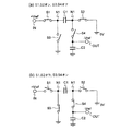
図1(a),(b)は、従来のチャージポンプ回路を説明するための回路構成図で、従来の負電圧を供給するための回路としては、図1(a),(b)に示すような電圧反転回路が提案されている(例えば、特許文献1参照)。チャージポンプ(Charge pump)とは、コンデンサとスイッチを組み合わせることによって電圧を上昇させるための電子回路である。
In recent years, based on the power supply voltage VDD and ground VSS supplied to LSI devices, the voltage is negatively boosted by a charge pump circuit, and the voltage (negative voltage) obtained by inverting the polarity of the power supply voltage VDD is used as a reference voltage. The power supply voltage range inside the LSI device may be expanded.
FIGS. 1A and 1B are circuit configuration diagrams for explaining a conventional charge pump circuit. As a conventional circuit for supplying a negative voltage, FIGS. 1A and 1B are shown. Such a voltage inverting circuit has been proposed (see, for example, Patent Document 1). A charge pump is an electronic circuit for raising a voltage by combining a capacitor and a switch.
上述した特許文献1に記載されている単一構成のチャージポンプ回路は、入力電圧+Vrefの電圧の極性を反転した電圧を出力するチャージポンプ回路である。図1(a),(b)に示したチャージポンプ回路は、2つのキャパシタC1、C2及びMOSFETスイッチS1〜S4から構成されている。入力端子INに+Vrefを印加した状態で、スイッチS1、S2をオンし、キャパシタC1に基準電圧Vrefを充電し、その後に、スイッチS3、S4をオンし、キャパシタC1の基準電圧Vrefは放電され、キャパシタC2に反転した電圧を充電する。この動作を繰り返すことにより、出力電圧として−Vrefを負荷に供給することができる。
The charge pump circuit having a single configuration described in
しかしながら、上述した従来のチャージポンプ回路は、充電と放電との切替えを一定の周期で行うと、その周期で充電及び放電の電流が瞬間的に流れ、切替えの周期(周波数)で大きな電磁ノイズが発生するという問題がある。チャージポンプ回路から所定の周波数で大きな電磁ノイズが発生すると、同じ周波数あるいはその高調波帯を利用する電子機器に悪影響を与えるEMI(Electromagnetic Interference:電磁干渉)が問題となる。そのため、電磁ノイズを抑制可能なチャージポンプ回路が必要である。しかしながら、上述した特許文献1には、充放電に起因する電磁ノイズを抑制することについては何ら念頭に置いていない。また、上述した特許文献1のチャージポンプ回路は、各スイッチを制御するためのスイッチ制御回路とクロック生成回路が別途必要となる。
However, in the conventional charge pump circuit described above, when switching between charging and discharging is performed at a constant cycle, charging and discharging currents instantaneously flow at that cycle, and large electromagnetic noise is generated at the switching cycle (frequency). There is a problem that occurs. When large electromagnetic noise is generated at a predetermined frequency from the charge pump circuit, EMI (Electromagnetic Interference) that adversely affects electronic equipment using the same frequency or its harmonic band becomes a problem. Therefore, a charge pump circuit that can suppress electromagnetic noise is required. However,
本発明は、このような問題に鑑みてなされたもので、その目的とするところは、キャパシタの充放電に伴って発生する電磁ノイズを抑制可能とし、かつスイッチ制御回路とクロック生成回路が不要なチャージポンプ回路を提供することにある。 The present invention has been made in view of such problems, and an object of the present invention is to make it possible to suppress electromagnetic noise generated due to charging / discharging of a capacitor and to eliminate the need for a switch control circuit and a clock generation circuit. The object is to provide a charge pump circuit.
本発明は、このような目的を達成するためになされたもので、請求項1に記載の発明は、キャパシタを充放電して電圧を昇降圧するチャージポンプ回路において、相補チャージポンプ回路を複数個設置し、該相補チャージポンプ回路の各入力電圧の電圧入力端子を並列接続し、前記相補チャージポンプ回路の各出力電圧の電圧出力端子を並列接続するように構成し、前段の相補チャージポンプ回路の出力クロックを、次段の相補チャージポンプ回路の入力クロックとなるよう接続し、連結された複数の前記相補チャージポンプ回路の動作クロックが重複しないように動作することを特徴とするチャージポンプ回路。(図5及び図9に対応)
The present invention has been made to achieve such an object, and the invention according to
また、請求項2に記載の発明は、請求項1に記載の発明において、前記連結された複数の相補チャージポンプ回路の動作クロックが重複しないように動作することで、1つの相補チャージポンプ回路がその入力電圧をそのフライングキャパシタに電化充電する期間は、他の相補チャージポンプ回路がそのフライングキャパシタの電化放電期間となり出力電圧を連続して生成することを特徴とする。 According to a second aspect of the present invention, in the first aspect of the present invention, one complementary charge pump circuit is configured to operate so that operation clocks of the plurality of connected complementary charge pump circuits do not overlap. During the period in which the input voltage is electrified and charged in the flying capacitor, another complementary charge pump circuit is in the electrification and discharge period of the flying capacitor, and the output voltage is continuously generated.
また、請求項3に記載の発明は、請求項1又は2に記載の発明において、前記連結された複数の相補チャージポンプ回路の最後段の前記相補チャージポンプ回路の出力クロックを、最前段の相補チャージポンプ回路の入力クロックとなるよう接続し、リング発振器を構成することを特徴とする。
また、請求項4に記載の発明は、請求項1乃至3のいずれかに記載の発明において、前記相補チャージポンプ回路は、第1のチャージポンプと第2のチャージポンプで構成され、前記第1のチャージポンプと前記第2のチャージポンプが相補動作することで、前記第1のチャージポンプと前記第2のチャージポンプが交互に各出力電圧を生成することを特徴とする。
According to a third aspect of the present invention, in the first or second aspect of the present invention, the output clock of the complementary charge pump circuit at the last stage of the plurality of connected complementary charge pump circuits is set to be complementary to the front stage. The ring oscillator is configured by connecting the charge pump circuit to be an input clock.
According to a fourth aspect of the present invention, in the invention according to any one of the first to third aspects, the complementary charge pump circuit includes a first charge pump and a second charge pump. The charge pump and the second charge pump operate in a complementary manner, so that the first charge pump and the second charge pump alternately generate output voltages.
また、請求項5に記載の発明は、請求項4に記載の発明において、前記第1のチャージポンプを構成する各スイッチと前記第2のチャージポンプを構成する各スイッチの制御を互いに相補制御することを特徴とする。
また、請求項6に記載の発明は、請求項1乃至3のいずれかに記載の発明において、前記相補チャージポンプ回路は、入力電圧(VDD)と基準電圧(VSS)と間で遷移するクロック信号(CKO111)が一端に入力される第1のキャパシタ(C111)と、該第1のキャパシタの他端に各入力端子が接続される第1及び第2のスイッチ(SW131,SW141)とを有し、前記第2のスイッチの出力端子から出力電圧を出力する第1のチャージポンプと、前記クロック信号の反転信号(CKO211)が一端に入力される第2のキャパシタ(C211)と、該第2のキャパシタの他端に接続される第3及び第4のスイッチ(SW231,SW241)とを有し、前記第4のスイッチの出力端子から出力電圧を出力する第2のチャージポンプとを備え、前記第1のキャパシタの他端の電圧に従い前記第3及び第4のスイッチがオンオフ制御され、前記第2のキャパシタの他端の電圧に従い前記第1及び第2のスイッチがオンオフ制御することで、前記第1のチャージポンプと前記第2のチャージポンプが交互に各出力電圧を出力することを特徴とする。(図2乃至図3に対応)
According to a fifth aspect of the present invention, in the fourth aspect of the present invention, the controls of the switches constituting the first charge pump and the switches constituting the second charge pump are complementarily controlled. It is characterized by that.
According to a sixth aspect of the present invention, in the invention according to any one of the first to third aspects, the complementary charge pump circuit has a clock signal that transitions between an input voltage (VDD) and a reference voltage (VSS). (CKO111) is the first capacitor that is input (C111) at one end, first and second switches each input terminal is connected to the other end of the first capacitor (SW 131, SW141) and has a a first charge pump for outputting an output voltage from the output terminal of the second switch, the inverted signal of the clock signal (CKO211) is a second capacitor that is input to one end (C211), the second third and fourth switches (SW231, SW241) and having a second charge outputting an output voltage from the output terminal of said fourth switch connected to the other end of the capacitor And a pump, wherein in accordance with the voltage of the other end of the first capacitor and the third and fourth switches are on-off controlled, said first and second switches are off in accordance with the voltage of the other end of said second capacitor By controlling, the first charge pump and the second charge pump alternately output each output voltage. (Corresponding to FIGS. 2 to 3)
また、請求項7に記載の発明は、請求項1乃至3のいずれかに記載の発明において、前記相補チャージポンプ回路は、入力電圧(VDD)と基準電圧(VSS)と間で遷移するクロック信号(CKO111)が一端に入力される第1のキャパシタ(C111)と、該第1のキャパシタの他端に各入力端子が接続される第1及び第2のスイッチ(SW131,SW141)とを有し、前記第2のスイッチの出力端子から出力電圧を出力する第1のチャージポンプとを備え、前記第1及び第2のスイッチがオンオフ制御することで、前記第1のチャージポンプが出力電圧を出力することを特徴とする。(図7及び図8に対応)
また、請求項8に記載の発明は、キャパシタを充放電して電圧を昇降圧するチャージポンプ回路において、相補チャージポンプ回路を複数個設置し、該相補チャージポンプ回路の各入力電圧の電圧入力端子を並列接続し、前記相補チャージポンプ回路の各出力電圧の電圧出力端子を並列接続するように構成し、前記相補チャージポンプ回路は、入力電圧と基準電圧と間で遷移するクロック信号が一端に入力される第1のキャパシタと、該第1のキャパシタの他端に各入力端子が接続される第1及び第2のスイッチとを有し、前記第2のスイッチの出力端子から出力電圧を出力する第1のチャージポンプと、前記クロック信号の反転信号が一端に入力される第2のキャパシタと、該第2のキャパシタの他端に接続される第3及び第4のスイッチとを有し、前記第4のスイッチの出力端子から出力電圧を出力する第2のチャージポンプとを備え、前記第1のキャパシタの他端の電圧に従い前記第3及び第4のスイッチがオンオフ制御され、前記第2のキャパシタの他端の電圧に従い前記第1及び第2のスイッチがオンオフ制御することで、前記第1のチャージポンプと前記第2のチャージポンプが交互に各出力電圧を出力することを特徴とする。
According to a seventh aspect of the present invention, in the invention according to any one of the first to third aspects, the complementary charge pump circuit is a clock signal that transitions between an input voltage (VDD) and a reference voltage (VSS). (CKO111) is the first capacitor that is input (C111) at one end, first and second switches each input terminal is connected to the other end of the first capacitor (SW 131, SW141) and has a the second and a first charge pump for outputting an output voltage from the switch output terminal, said that the first and second switches are on-off control, it outputs the first charge pump output voltage It is characterized by doing. (Corresponding to FIGS. 7 and 8)
According to an eighth aspect of the present invention, a plurality of complementary charge pump circuits are provided in a charge pump circuit that charges and discharges a capacitor to increase / decrease a voltage, and voltage input terminals for each input voltage of the complementary charge pump circuit are provided. The complementary charge pump circuit is connected in parallel and the voltage output terminals of the respective output voltages of the complementary charge pump circuit are connected in parallel. The complementary charge pump circuit receives a clock signal that transitions between an input voltage and a reference voltage at one end. a first capacitor that, and first and second switches each input terminal is connected to the other end of the first capacitor, the output of the output voltage from the output terminal of the second switch a first charge pump, the third and fourth switch inverted signal of the clock signal is connected to the second capacitor is input to one end, the other end of the second capacitor It has, and a second charge pump for outputting an output voltage from the output terminal of the fourth switch, the first of the accordance voltage at the other end of the capacitor and the third and fourth switches are on-off controlled the by second other end said first and second switches in accordance with the voltage of the capacitor is on-off control, that the first charge pump and the second charge pump outputs each output voltage alternately It is characterized by.
本発明によれば、複数個の相補チャージポンプ回路を設置接続することで、キャパシタの充放電に伴って発生する電磁ノイズを分散させ、また、複数個の相補チャージポンプ回路のクロック接続系を自己発振させることで、動作クロックを自己生成する。このため、チャージポンプ回路の電磁ノイズを抑制でき、かつスイッチ制御回路とクロック生成回路が不要となる。したがって、キャパシタの充放電に伴って発生する電磁ノイズを抑制可能とし、かつスイッチ制御回路とクロック生成回路が不要なチャージポンプ回路が実現できる。 According to the present invention, a plurality of complementary charge pump circuits are installed and connected to disperse electromagnetic noise generated due to charging and discharging of the capacitors, and the clock connection system of the plurality of complementary charge pump circuits can be self-configured. By oscillating, the operation clock is self-generated. For this reason, the electromagnetic noise of the charge pump circuit can be suppressed, and the switch control circuit and the clock generation circuit become unnecessary. Therefore, it is possible to realize a charge pump circuit that can suppress electromagnetic noise generated due to charging and discharging of the capacitor and that does not require a switch control circuit and a clock generation circuit.
以下、図面を参照して本発明の各実施形態について説明する。
<実施形態1>
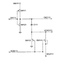
図2は、本発明に係るチャージポンプ回路を構成する相補チャージポンプ回路の実施形態1を説明するための回路構成図である。図中符号20は相補チャージポンプ回路を示している。
Hereinafter, each embodiment of the present invention will be described with reference to the drawings.
<
FIG. 2 is a circuit configuration diagram for explaining the first embodiment of the complementary charge pump circuit constituting the charge pump circuit according to the present invention.
まず、本発明の相補チャージポンプ回路が、Nウェル(N−well)を備えたP型基板上に構成されるものとして説明する。なお、ここでは、素子遅延はないものとして動作を説明する。
図2に示した相補チャージポンプ回路は、スイッチSW111〜SW141とフライングキャパシタC111で構成される第1のチャージポンプと、スイッチSW211〜SW241とフライングキャパシタC211で構成される第2のチャージポンプとを有する。以下では、フライングキャパシタC111の電極のうち、SW111側を第1電極、SW131側を第2電極という。フライングキャパシタC211の電極のうち、SW211側を第1電極、SW231側を第2電極という。
First, the complementary charge pump circuit according to the present invention will be described as being configured on a P-type substrate having an N-well. Here, the operation will be described assuming that there is no element delay.
The complementary charge pump circuit shown in FIG. 2 includes a first charge pump composed of switches SW111 to SW141 and a flying capacitor C111, and a second charge pump composed of switches SW211 to SW241 and a flying capacitor C211. . Hereinafter, among the electrodes of the flying capacitor C111, the SW111 side is referred to as a first electrode, and the SW131 side is referred to as a second electrode. Of the electrodes of the flying capacitor C211, the SW211 side is referred to as a first electrode and the SW231 side is referred to as a second electrode.
第1のチャージポンプのSW111、SW131は、PMOSトランジスタであり、SW121、SW141は、NMOSトランジスタとなる。SW111は、フライングキャパシタC111の第1電極と入力端子VIN111との間に接続される。SW121は、フライングキャパシタC111の第1電極と接地端子との間に接続される。SW131は、フライングキャパシタC111の第2電極と接地端子との間に接続される。SW141は、フライングキャパシタC111の第2電極と出力端子VOUT111との間に接続される。SW141のバックゲート端子は、SW141がラッチアップするのを防止するためにVOUT111に接続される。SW111、SW121のゲート端子は、入力クロック端子CKI111に接続される。SW131、SW141のゲート端子は、第2のチャージポンプのフライングキャパシタC211の第2電極に接続される。SW111とSW121で構成されるインバータ出力は、出力クロック端子CKO111となる。 SW111 and SW131 of the first charge pump are PMOS transistors, and SW121 and SW141 are NMOS transistors. The SW111 is connected between the first electrode of the flying capacitor C111 and the input terminal VIN111. The SW 121 is connected between the first electrode of the flying capacitor C111 and the ground terminal. The SW 131 is connected between the second electrode of the flying capacitor C111 and the ground terminal. The SW 141 is connected between the second electrode of the flying capacitor C111 and the output terminal VOUT111. The back gate terminal of SW 141 is connected to VOUT 111 to prevent SW 141 from latching up. The gate terminals of SW111 and SW121 are connected to the input clock terminal CKI111. The gate terminals of SW131 and SW141 are connected to the second electrode of the flying capacitor C211 of the second charge pump. The inverter output composed of SW111 and SW121 becomes an output clock terminal CKO111.
第2のチャージポンプのSW211、SW231は、PMOSトランジスタであり、SW221、SW241は、NMOSトランジスタとなる。SW211は、フライングキャパシタC211の第1電極と入力端子VIN211との間に接続される。SW221は、フライングキャパシタC211の第1電極と接地端子との間に接続される。SW231は、フライングキャパシタC211の第2電極と接地端子との間に接続される。SW241は、フライングキャパシタC211の第2電極と出力端子VOUT211との間に接続される。SW241のバックゲート端子は、SW241がラッチアップするのを防止するためにVOUT211に接続される。SW211、SW221のゲート端子は、CKO111に接続される。SW231、SW241のゲート端子は、第1のチャージポンプのフライングキャパシタC111の第2電極に接続される。SW211とSW221で構成されるインバータ出力は、出力クロック端子CKO211となる。第1のチャージポンプの入力端子VIN111と第2のチャージポンプの出力端子VIN211は、VIN端子に共通接続される。第1のチャージポンプの出力端子VOUT111と第2のチャージポンプの出力端子VOUT211は、VOUT端子に共通接続され、VOUT端子には安定化キャパシタCoutが接地接続されている。
SW211 and SW231 of the second charge pump are PMOS transistors, and SW221 and SW241 are NMOS transistors. The
図3(a)乃至(f)は、図2に示した相補チャージポンプ回路の動作タイミング・チャートを示す図である。ただし、クロック入力前の初期状態では、各フライングキャパシタの充電電圧は0Vとする。入力端子VINは電源電圧VDDを印加した状態とする。
クロックCKI111にVDDを入力開始直後、区間[1]において、ノードCKO111はVSS、ノードCKO211はVDD、ノードVCK111はVSS、ノードVCK211はVDDとなる。このときSW231はオンし、フライングキャパシタC211を充電する。C211の充電によりノードVCK211の電圧レベルがVDDから徐々に下降し、この下降分をV1とする。このときSW131はオフする。また、このとき、SW141はオンし、VCK111の電圧VSSがVOUT111に出力されVOUT端子のキャパシタCoutに充電される。このとき、SW241はオフする。
FIGS. 3A to 3F are operation timing charts of the complementary charge pump circuit shown in FIG. However, in the initial state before the clock input, the charging voltage of each flying capacitor is 0V. The input terminal VIN is in a state where the power supply voltage VDD is applied.
Immediately after starting to input VDD to the clock CKI111, in the interval [1], the node CKO111 is VSS, the node CKO211 is VDD, the node VCK111 is VSS, and the node VCK211 is VDD. At this time, the SW 231 is turned on and the flying capacitor C211 is charged. The voltage level of the node VCK211 gradually decreases from VDD due to the charging of C211 and this decreased amount is set to V1. At this time, SW 131 is turned off. At this time, the SW 141 is turned on, the voltage VSS of the VCK 111 is output to the VOUT 111, and the capacitor Cout of the VOUT terminal is charged. At this time, SW241 is turned off.
次の区間[2]において、クロックCKI111がVSSのとき、CKO111はVDD、CKO211はVSSとなり、このときVCK211はC211の充電電圧V211よりVSS−V1となり、SW131がオンしてフライングキャパシタC111を充電する。C111の充電によりVCK111の電位がVDDから徐々に下降し、この下降分をV2とする。このときSW231はオフする。また、このとき、SW241はオンし、VCK211の電圧VSS−V1がVOUT211に出力されVOUT端子のキャパシタCoutに充電される。このとき、SW141はオフする。
In the next section [2], when the clock CKI111 is VSS, CKO111 becomes VDD and CKO211 becomes VSS. At this time, VCK211 becomes VSS-V1 from the charging voltage V211 of C211 and SW131 is turned on to charge the flying capacitor C111. . Due to the charging of C111, the potential of VCK111 gradually decreases from VDD, and this decrease is set to V2. At this time, SW231 is turned off. At this time, the SW 241 is turned on, the voltage VSS-V1 of the
次の区間[3]において、クロックCKI111がVDDのとき、VCK111はC111の充電電圧V2よりVSS−V2となり、SW231がオンしてC211を充電する。このとき、SW141はオンし、VCK111の電圧VSS−V2がVOUT111に出力されVOUT端子のキャパシタCoutに充電される。
以下CKI111が位相反転するごとに同様の動作を繰り返すことで、C111とC211の充電電圧は上昇し、最終的にVDDとなることで、VOUT111とVOUT211は交互に−VDDが出力され、VOUT端子は安定的に−VDDとなりキャパシタCoutに充電される。
In the next section [3], when the clock CKI111 is VDD, VCK111 becomes VSS-V2 from the charging voltage V2 of C111, and SW231 is turned on to charge C211. At this time, the SW 141 is turned on, and the voltage VSS-V2 of the VCK 111 is output to the VOUT 111 and charged to the capacitor Cout of the VOUT terminal.
Thereafter, the same operation is repeated every time the phase of CKI111 is inverted, so that the charging voltage of C111 and C211 rises and finally becomes VDD, so that VOUT111 and VOUT211 alternately output -VDD, and the VOUT terminal The voltage is stably −VDD, and the capacitor Cout is charged.
上述したように、本発明の相補チャージポンプ回路は、第1のチャージポンプと第2のチャージポンプで構成され、第1のチャージポンプと第2のチャージポンプが相補動作することで、第1のチャージポンプと第2のチャージポンプが交互に出力電圧を生成することを特徴とするチャージポンプ回路である。
また、第1のチャージポンプを構成する各スイッチと第2のチャージポンプを構成する各スイッチの制御を、互いに相補制御することで、外部スイッチ制御回路を不要とすることを特徴とするチャージポンプ回路である。
As described above, the complementary charge pump circuit of the present invention is configured by the first charge pump and the second charge pump, and the first charge pump and the second charge pump are operated in a complementary manner. The charge pump circuit is characterized in that the charge pump and the second charge pump alternately generate an output voltage.
A charge pump circuit characterized in that an external switch control circuit is not required by controlling the switches constituting the first charge pump and the switches constituting the second charge pump in a complementary manner. It is.
図4は、本発明に係るチャージポンプ回路を構成する相補チャージポンプ回路の実施形態1の他の例を説明するための回路構成図である。図中符号40は相補チャージポンプ回路を示している。
図2に示した負電圧を出力生成する相補チャージポンプ回路に対して、図4に示すように、第1のチャージポンプのSW141をPMOSトランジスタ、SW131をNMOSトランジスタとし、第2のチャージポンプのSW241をPMOSトランジスタ、SW131をNMOSトランジスタとすることで、入力端子VINに入力電圧VDDを印加したとき、出力電圧に2xVDDの昇電圧を出力生成する構成としてもよい。
FIG. 4 is a circuit configuration diagram for explaining another example of the first embodiment of the complementary charge pump circuit constituting the charge pump circuit according to the present invention.
In contrast to the complementary charge pump circuit that generates and outputs the negative voltage shown in FIG. 2, as shown in FIG. 4, the SW141 of the first charge pump is a PMOS transistor, the SW131 is an NMOS transistor, and the SW241 of the second charge pump is used. The PMOS transistor and the SW 131 are NMOS transistors, so that when the input voltage VDD is applied to the input terminal VIN, an output voltage of 2 × VDD is generated as an output voltage.
つまり、本発明に係る相補チャージポンプ回路は、入力電圧VDDと基準電圧VSSと間で遷移するクロック信号CKO111が一端に入力される第1のキャパシタC111と、この第1キャパシタの他端に各入力端子が接続される第1及び第2のスイッチSW131,SW141とを有し、第2スイッチの出力端子から出力電圧を出力する第1のチャージポンプと、クロック信号の反転信号CKO211が一端に入力される第2のキャパシタC211と、この第2キャパシタの他端に接続される第3及び第4のスイッチSW231,SW241とを有し、第4スイッチの出力端子から出力電圧を出力する第2のチャージポンプとを備え、第1キャパシタの他端の電圧に従い第3及び第4のスイッチがオンオフ制御され、第2キャパシタの他端の電圧に従い第1及び第2のスイッチがオンオフ制御することで、第1のチャージポンプと第2のチャージポンプが交互に各出力電圧を出力する。 That is, in the complementary charge pump circuit according to the present invention, the first capacitor C111 having the clock signal CKO111 transitioning between the input voltage VDD and the reference voltage VSS input to one end and the other input to the other end of the first capacitor. A first charge pump that has first and second switches SW131 and SW141 to which terminals are connected, outputs an output voltage from an output terminal of the second switch, and an inverted signal CKO211 of a clock signal is input to one end. A second capacitor C211 and third and fourth switches SW231 and SW241 connected to the other end of the second capacitor, and outputs an output voltage from the output terminal of the fourth switch. And the third and fourth switches are controlled to be turned on / off according to the voltage at the other end of the first capacitor. The first and second switches in accordance with the voltage by on-off control, the first charge pump and a second charge pump outputs each output voltage alternately.
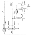
図5は、本発明に係るチャージポンプ回路の実施例1を説明するための回路ブロック図で、図2又は図4に示した相補チャージポンプ回路をN個設けたチャージポンプ回路を示している。図中符号101乃至10Nは相補チャージポンプ回路、111乃至11N及び211乃至21Nはチャージポンプを示している。
本発明に係る相補チャージポンプ回路を複数個設置し、この相補チャージポンプ回路の各入力電圧の電圧入力端子を並列接続し、相補チャージポンプ回路の各出力電圧の電圧出力端子を並列接続するように構成する。
FIG. 5 is a circuit block diagram for explaining
A plurality of complementary charge pump circuits according to the present invention are installed, voltage input terminals for each input voltage of the complementary charge pump circuit are connected in parallel, and voltage output terminals for each output voltage of the complementary charge pump circuit are connected in parallel. Configure.
また、前段の相補チャージポンプ回路の出力クロックを、次段の相補チャージポンプ回路の入力クロックとなるよう接続し、連結された複数の相補チャージポンプ回路の動作クロックが重複しないように動作する。
また、連結された複数の相補チャージポンプ回路の動作クロックが重複しないように動作することで、1つの相補チャージポンプ回路がその入力電圧をそのフライングキャパシタに電化充電する期間は、他の相補チャージポンプ回路がそのフライングキャパシタの電化放電期間となり出力電圧を連続して生成する。
Further, the output clock of the complementary charge pump circuit at the previous stage is connected to be the input clock of the complementary charge pump circuit at the next stage, and the operation clocks of the plurality of coupled complementary charge pump circuits are operated so as not to overlap.
In addition, by operating so that the operation clocks of a plurality of connected complementary charge pump circuits do not overlap each other, the period during which one complementary charge pump circuit electrifies and charges the input voltage to the flying capacitor is another complementary charge pump. The circuit becomes an electrification discharge period of the flying capacitor and continuously generates an output voltage.
また、連結された複数の相補チャージポンプ回路の最後段の相補チャージポンプ回路の出力クロックを、最前段の相補チャージポンプ回路の入力クロックとなるよう接続し、リング発振器を構成する。
また、相補チャージポンプ回路は、第1のチャージポンプと第2のチャージポンプで構成され、第1のチャージポンプと第2のチャージポンプが相補動作することで、第1のチャージポンプと第2のチャージポンプが交互に各出力電圧を生成する。
Further, the output clock of the last complementary charge pump circuit of the plurality of connected complementary charge pump circuits is connected to become the input clock of the front complementary charge pump circuit to constitute a ring oscillator.
The complementary charge pump circuit is composed of a first charge pump and a second charge pump, and the first charge pump and the second charge pump are operated in a complementary manner, whereby the first charge pump and the second charge pump are operated. The charge pump generates each output voltage alternately.
また、第1のチャージポンプを構成する各スイッチと第2のチャージポンプを構成する各スイッチの制御を互いに相補制御する。
図5に示したチャージポンプ回路は、相補チャージポンプ回路001〜00Nで構成されている。相補チャージポンプ回路00Nは、スイッチSW11N〜SW14NとフライングキャパシタC11Nで構成されるチャージポンプ11Nと、スイッチSW21N〜SW24NとフライングキャパシタC21Nで構成されるチャージポンプ21Nを備え、これにより、本実施例1は、Nx2個の相補チャージポンプで構成されている。
In addition, the controls of the switches constituting the first charge pump and the switches constituting the second charge pump are complementarily controlled.
The charge pump circuit shown in FIG. 5 includes complementary charge pump circuits 001 to 00N. The complementary charge pump circuit 00N includes a
入力端子VINは、相補チャージポンプ回路00NのVIN11NとVIN21Nに共通接続される。出力端子VOUTは、相補チャージポンプ回路00NのVOUT11NとVOUT21Nに共通接続される。出力端子VOUTには安定化キャパシタCoutが接地接続される。
相補チャージポンプ回路001のクロック入力端CKI111には、相補チャージポンプ回路00Nの出力クロックCKO11Nが接続される。相補チャージポンプ回路00Nのクロック入力端CKI00Nには、相補チャージポンプ回路00(N−1)の出力クロックCKO11(N−1)が接続される。
The input terminal VIN is commonly connected to VIN11N and VIN21N of the complementary charge pump circuit 00N. The output terminal VOUT is commonly connected to VOUT11N and VOUT21N of the complementary charge pump circuit 00N. A stabilization capacitor Cout is connected to the output terminal VOUT.
The output clock CKO11N of the complementary charge pump circuit 00N is connected to the clock input terminal CKI111 of the complementary charge pump circuit 001. The output clock CKO11 (N-1) of the complementary charge pump circuit 00 (N-1) is connected to the clock input terminal CKI00N of the complementary charge pump circuit 00N.
これにより、図2又は図4で示す相補チャージポンプ001のチャージポンプ111におけるSW111とSW121で構成されるインバータから出力されるクロックCKO111が、本実施例1では、クロックCKO111〜クロックCKO11Nは奇数の位相反転するクロック系により、リング発振器を構成する。
相補チャージポンプ回路00Nのチャージポンプ11NにおけるスイッチSW11N〜SW14Nは、図1に示した従来の単一構成のチャージポンプ回路のスイッチS1〜S4に対して各々1/(Nx2)倍のサイズとし、フライングキャパシタC11Nは、図1に示した単一構成のチャージポンプ回路のキャパシタC1に対して各々1/(Nx2)倍のサイズとする。同様に相補チャージポンプ回路00Nのチャージポンプ21NにおけるスイッチSW21N〜SW24Nは、図1に示した単一構成のチャージポンプ回路のスイッチS1〜S4に対して各々1/(Nx2)倍のサイズとし、フライングキャパシタC21Nは、図1に示した単一構成のチャージポンプ回路のキャパシタC1に対して各々1/(Nx2)倍のサイズとする。
As a result, the clock CKO111 output from the inverter composed of SW111 and SW121 in the charge pump 111 of the complementary charge pump 001 shown in FIG. 2 or FIG. 4 is an odd phase in the clock CKO111 to the clock CKO11N in the first embodiment. A ring oscillator is constituted by a clock system that is inverted.
The switches SW11N to SW14N in the
図6(a),(b)は、図5に示したチャージポンプ回路の動作タイミング・チャートを示す図である。相補チャージポンプ回路00(N−1)の出力クロックCKO11(N−1)と相補チャージポンプ回路00Nの出力クロックCKO11Nには時間t1の素子遅延があるものとする。
区間[a1]において、相補チャージポンプ回路00Nの出力クロックCKO11NがVDDのとき、位相反転した時間t1遅延する相補チャージポンプ回路00NのクロックCKO21Nと相補チャージポンプ回路001のクロックCKO111がVSSとなり、チャージポンプ21NのフライングキャパシタC211は放電されVOUTのキャパシタCoutに−VDDを充電開始、及びチャージポンプ111のフライングキャパシタC111は放電されVOUTのキャパシタCoutに−VDDを充電開始する。このときタイミングa1Tでチャージポンプ21Nとチャージポンプ111の電磁ノイズが発生する。
6A and 6B are diagrams showing operation timing charts of the charge pump circuit shown in FIG. Assume that there is an element delay of time t1 between the output clock CKO11 (N-1) of the complementary charge pump circuit 00 (N-1) and the output clock CKO11N of the complementary charge pump circuit 00N.
In the interval [a1], when the output clock CKO11N of the complementary charge pump circuit 00N is VDD, the clock CKO21N of the complementary charge pump circuit 00N and the clock CKO111 of the complementary charge pump circuit 001 that are delayed by the phase inversion time t1 become VSS, and the charge pump. The 21N flying capacitor C211 is discharged to start charging -VDD to the VOUT capacitor Cout, and the flying capacitor C111 of the charge pump 111 is discharged to start charging -VDD to the VOUT capacitor Cout. At this time, electromagnetic noise of the
区間[b2]において、クロックCK0111に対し、位相反転した時間t1遅延する相補チャージポンプ回路001のクロックCKO211と相補チャージポンプ回路002のクロックCKO112がVDDとなり、チャージポンプ211のフライングキャパシタC211にVDDを充電開始、及びチャージポンプ112のフライングキャパシタC112にVDDを充電開始する。このとき、タイミングb2Tでチャージポンプ211とチャージポンプ112の電磁ノイズが発生する。
In the interval [b2], the clock CKO211 of the complementary charge pump circuit 001 and the clock CKO112 of the complementary charge pump circuit 002 that are delayed by the time t1 that is phase-inverted with respect to the clock CK0111 become VDD, and the flying capacitor C211 of the
区間[a3]において、クロックCKO112に対し、位相反転した時間t1遅延する相補チャージポンプ回路002のクロックCKO212と相補チャージポンプ回路003のクロック113がVSSとなり、チャージポンプ212のフライングキャパシタC212は放電されVOUTのキャパシタCoutに−VDDを充電開始、及びチャージポンプ113のフライングキャパシタC113は放電されVOUTのキャパシタCoutに−VDDを充電開始する。このとき、タイミングa3Tでチャージポンプ212とチャージポンプ113の電磁ノイズが発生する。 In the interval [a3], the clock CKO212 of the complementary charge pump circuit 002 and the clock 113 of the complementary charge pump circuit 003, which are delayed by the time t1 after the phase inversion with respect to the clock CKO112, become VSS, and the flying capacitor C212 of the charge pump 212 is discharged and VOUT. -VDD starts to be charged to -VDD, and the flying capacitor C113 of the charge pump 113 is discharged to start charging -VDD to the VOUT capacitor Cout. At this time, electromagnetic noise of the charge pump 212 and the charge pump 113 is generated at the timing a3T.
区間[aN]において、相補チャージポンプ回路00(N−1)の出力クロックCK011(N−1)がVDDのとき、位相反転した時間t1遅延する相補チャージポンプ回路00(N−1)のクロックCKO21(N−1)と相補チャージポンプ回路00NのクロックCKO11NがVSSとなり、チャージポンプ21(N−1)のフライングキャパシタC21(N−1) は放電されVOUTのキャパシタCoutに−VDDを充電開始、及びチャージポンプ11NのフライングキャパシタC11Nは放電されVOUTのキャパシタCoutに−VDDを充電開始する。このとき、タイミングaNTでチャージポンプ21(N−1)とチャージポンプ11Nの電磁ノイズが発生する。
In the interval [aN], when the output clock CK011 (N-1) of the complementary charge pump circuit 00 (N-1) is VDD, the clock CKO21 of the complementary charge pump circuit 00 (N-1) delayed by the phase inverted time t1. (N-1) and the clock CKO11N of the complementary charge pump circuit 00N become VSS, the flying capacitor C21 (N-1) of the charge pump 21 (N-1) is discharged, and -VDD starts to be charged to the capacitor Cout of VOUT, and The flying capacitor C11N of the
区間[b1]において、クロックCKO11Nに対し、位相反転した時間t1遅延する相補チャージポンプ回路00NのクロックCKO21Nと相補チャージポンプ回路001のクロックCKO111がVDDとなり、チャージポンプ21NのフライングキャパシタC21NにVDDを充電開始、及びチャージポンプ111のフライングキャパシタC111にVDDを充電開始する。このときタイミングb1Tでチャージポンプ21Nとチャージポンプ111の電磁ノイズが発生する。
In the interval [b1], the clock CKO21N of the complementary charge pump circuit 00N and the clock CKO111 of the complementary charge pump circuit 001 that are delayed by the time t1 phase-inverted with respect to the clock CKO11N become VDD, and the flying capacitor C21N of the
区間[a2]において、クロックCK0111に対し、位相反転した時間t1遅延する相補チャージポンプ回路001のクロックCKO211と相補チャージポンプ回路002のクロックCKO112がVSSとなり、チャージポンプ211のフライングキャパシタC211は放電されVOUTのキャパシタCoutに−VDDを充電開始、及びチャージポンプ112のフライングキャパシタC112は放電されVOUTのキャパシタCoutに−VDDを充電開始する。このとき、タイミングa2Tでチャージポンプ211とチャージポンプ112の電磁ノイズが発生する。
In the interval [a2], the clock CKO211 of the complementary charge pump circuit 001 and the clock CKO112 of the complementary charge pump circuit 002 that are delayed by the phase t1 of the phase inversion with respect to the clock CK0111 become VSS, and the flying capacitor C211 of the
区間[b3]において、クロックCKO112に対し、位相反転した時間t1遅延する相補チャージポンプ回路002のクロックCKO212と相補チャージポンプ回路003のクロック113がVDDとなり、チャージポンプ212のフライングキャパシタC212にVDDを充電開始、及びチャージポンプ113のフライングキャパシタC113にVDDを充電開始する。このとき、タイミングb3Tでチャージポンプ212とチャージポンプ113の電磁ノイズが発生する。 In the interval [b3], the clock CKO212 of the complementary charge pump circuit 002 and the clock 113 of the complementary charge pump circuit 003 that are delayed by the phase t1 inverted from the clock CKO112 become VDD, and the flying capacitor C212 of the charge pump 212 is charged with VDD. Start and charging of the flying capacitor C113 of the charge pump 113 with VDD is started. At this time, electromagnetic noise of the charge pump 212 and the charge pump 113 is generated at the timing b3T.
区間[bN]において、相補チャージポンプ回路00(N−1)の出力クロックCK011(N−1)がVSSのとき、位相反転した時間t1遅延する相補チャージポンプ回路00(N−1)のクロックCKO21(N−1)と相補チャージポンプ回路00NのクロックCKO11NがVDDとなり、チャージポンプ21(N−1)のフライングキャパシタC21(N−1)にVDDを充電開始、及びチャージポンプ11NのフライングキャパシタC11NにVDDを充電開始する。このとき、タイミングbNTでチャージポンプ21(N−1)とチャージポンプ11Nの電磁ノイズが発生する。
In the interval [bN], when the output clock CK011 (N-1) of the complementary charge pump circuit 00 (N-1) is VSS, the clock CKO21 of the complementary charge pump circuit 00 (N-1) delayed by the phase inverted time t1. (N-1) and the clock CKO11N of the complementary charge pump circuit 00N become VDD, the charging of the flying capacitor C21 (N-1) of the charge pump 21 (N-1) is started, and the flying capacitor C11N of the
以降、上述した区間[a1]乃至区間[bN]の動作を繰り返す。
上述した動作により、区間aNでは、同位相で動作する相補チャージポンプ回路00(N−1)におけるチャージポンプ21(N−1)と相補チャージポンプ回路00Nにおけるチャージポンプ11Nは、タイミングaNTのフライングキャパシタ電化放電時、図1に示した単一構成のチャージポンプ回路の電磁ノイズの1/(2xN)倍の電磁ノイズが各々発生し、合わさることで1/N倍の電磁ノイズとなる。また、区間bNでは、同位相で動作する相補チャージポンプ回路00(N−1)におけるチャージポンプ21(N−1)と相補チャージポンプ回路00Nにおけるチャージポンプ11Nは、タイミングbNTのフライングキャパシタ電化充電時、図1に示した単一構成のチャージポンプ回路の電磁ノイズの1/(2xN)倍の電磁ノイズが各々発生し、合わさることで1/N倍の電磁ノイズとなる。
Thereafter, the operations in the section [a1] to the section [bN] described above are repeated.
Through the above-described operation, in the section aN, the charge pump 21 (N-1) in the complementary charge pump circuit 00 (N-1) operating in the same phase and the
また、クロックCKO111〜クロックCKO11Nにて奇数の位相反転するクロック系により構成されるリング発振器により、クロックCKO111〜クロックCKO11Nは各々がt1遅延するt1xN周期のクロックとなる。
また、区間aNで同位相で動作する相補チャージポンプ回路00(N−1)におけるチャージポンプ21(N−1)と相補チャージポンプ回路00Nの2個のチャージポンプがフライングキャパシタへの充電期間、それ以外の2xN−2個のチャージポンプは放電期間であり、VOUT端子のキャパシタCoutへ電化充電しているため、負荷への電圧供給能力は、図1で示す単一チャージポンプ回路の充放電周期をt1xNとしたときと同等である。
Also, the clocks CKO111 to CKO11N are clocks having a cycle of t1 × N each delayed by t1 by a ring oscillator configured by a clock system that inverts an odd number of phases with the clocks CKO111 to CKO11N.
In addition, in the complementary charge pump circuit 00 (N-1) operating in the same phase in the section aN, two charge pumps of the charge pump 21 (N-1) and the complementary charge pump circuit 00N are charged to the flying capacitor, Since the 2 × N−2 charge pumps other than those are in the discharge period and are electrically charged to the capacitor Cout of the VOUT terminal, the voltage supply capability to the load is the charge / discharge cycle of the single charge pump circuit shown in FIG. This is equivalent to t1xN.
これにより、本実施例1から発生する電磁ノイズは、図1に示した単一構成のチャージポンプ回路のそれに対し、時間t1間隔で1/N倍で発生する。よって本実施例1で発生する電磁ノイズは、図1に示した単一構成のチャージポンプ回路のそれに対して、1/N倍程度に抑圧されることになる。
さらに、本実施例1は、リング発振動作によるチャージポンプクロックを自己生成することで、デバイス内部にクロック生成回路は設置不要とし、またはデバイス外部からクロック供給を不要とすることで、付随するデバイスピンや関連する制御回路も不要となる。このため、デバイス面積を小さくすることができる。
As a result, the electromagnetic noise generated from the first embodiment is generated at a time interval of t1 at 1 / N times that of the charge pump circuit having the single configuration shown in FIG. Therefore, the electromagnetic noise generated in the first embodiment is suppressed to about 1 / N times that of the charge pump circuit having a single configuration shown in FIG.
Further, in the first embodiment, the charge pump clock by the ring oscillation operation is self-generated, so that the clock generation circuit is not required to be installed inside the device or the clock supply from the outside of the device is not required. And related control circuits are also unnecessary. For this reason, a device area can be made small.
なお、上述した実施例1は、一例を示したもので、この構成に限定されるものではない。つまり、相補チャージポンプ回路00Nのチャージポンプ11NにおけるスイッチSW11N〜SW14NとフライングキャパシタC11N、チャージポンプ21NにおけるスイッチSW21N〜SW24NとフライングキャパシタC21Nは、負荷への出力電圧の必要供給能力に応じて、それ本実施形態で示したサイズ以下としてもよく、電磁ノイズの抑制効果を高めることが可能である。
In addition, Example 1 mentioned above showed an example, and is not limited to this structure. That is, the switches SW11N to SW14N and the flying capacitor C11N in the
また、相補チャージポンプ回路001〜00Nにおける各クロックCKO111〜CK00Nのクロック間隔として時間t1を素子遅延としているが、相補チャージポンプ回路00Nのチャージポンプ11NにおけるスイッチSW11N〜SW14NとフライングキャパシタC11N、チャージポンプ21NにおけるスイッチSW21N〜SW24NとフライングキャパシタC21Nのサイズを調整することで、時間t1以上、またはそれ以下とすることも可能である。及び、連結するチャージポンプ回路の各出力クロックの間に遅延素子を設置することで、クロック間隔を時間t2以上とすることも可能である。
The time t1 is an element delay as the clock interval of the clocks CKO111 to CK00N in the complementary charge pump circuits 001 to 00N. However, the switches SW11N to SW14N, the flying capacitor C11N, and the
また、本実施例1では、VOUT端子のキャパシタCoutは出力電圧安定化のために設置しているが、区間aNで同位相で動作する相補チャージポンプ回路00(N−1)におけるチャージポンプ21(N−1)と相補チャージポンプ回路00Nの2個のチャージポンプがフライングキャパシタへの充電期間、それ以外の2xN−2個のチャージポンプは放電期間であり、VOUT端子のキャパシタCoutへ電化充電しているため、全期間で安定した出力電圧を得ることができるため、キャパシタCoutは設置しなくてもよい。
また、本実施例1では、相補チャージポンプ回路001のクロック入力端に、相補チャージポンプ回路00Nの出力クロックCKO11Nを接続することでリング発振動作によるチャージポンプクロックを自己生成しているが、本接続を削除し、相補チャージポンプ回路001のクロック入力端に外部供給クロックを入力してもよい。
In the first embodiment, the capacitor Cout at the VOUT terminal is provided for stabilizing the output voltage, but the charge pump 21 (in the complementary charge pump circuit 00 (N−1) operating in the same phase in the section aN. N-1) and two charge pumps of the complementary charge pump circuit 00N are charging periods for the flying capacitors, and the other 2 × N−2 charge pumps are discharging periods, and are electrified and charged to the capacitor Cout of the VOUT terminal. Therefore, since a stable output voltage can be obtained over the entire period, the capacitor Cout need not be installed.
In the first embodiment, the charge pump clock by the ring oscillation operation is self-generated by connecting the output clock CKO11N of the complementary charge pump circuit 00N to the clock input terminal of the complementary charge pump circuit 001. And an externally supplied clock may be input to the clock input terminal of the complementary charge pump circuit 001.
<実施形態2>
図7は、本発明に係るチャージポンプ回路を構成する相補チャージポンプ回路の実施形態2を説明するための回路構成図で、図2に示した相補チャージポンプ回路における第1チャージポンプのみで構成される相補チャージポンプ回路を示している。スイッチSW111〜SW141とフライングキャパシタC111で構成される。SW111、SW131は、PMOSトランジスタであり、SW121、SW141は、NMOSトランジスタとなる。SW111は、フライングキャパシタC111の第1電極と入力端子VIN111との間に接続される。SW121は、フライングキャパシタC111の第1電極と接地端子との間に接続される。SW131は、フライングキャパシタC111の第2電極と接地端子との間に接続される。SW141は、フライングキャパシタC111の第2電極と出力端子VOUT111との間に接続される。SW141のバックゲート端子は、SW141がラッチアップするのを防止するためにVOUT111に接続される。SW111、SW121のゲート端子は、入力クロック端子CKI001に接続される。
<
FIG. 7 is a circuit configuration diagram for explaining a second embodiment of the complementary charge pump circuit constituting the charge pump circuit according to the present invention, and is composed only of the first charge pump in the complementary charge pump circuit shown in FIG. 2 shows a complementary charge pump circuit. The switches SW111 to SW141 and the flying capacitor C111 are included. SW111 and SW131 are PMOS transistors, and SW121 and SW141 are NMOS transistors. The SW111 is connected between the first electrode of the flying capacitor C111 and the input terminal VIN111. The SW 121 is connected between the first electrode of the flying capacitor C111 and the ground terminal. The SW 131 is connected between the second electrode of the flying capacitor C111 and the ground terminal. The SW 141 is connected between the second electrode of the flying capacitor C111 and the output terminal VOUT111. The back gate terminal of SW 141 is connected to VOUT 111 to prevent SW 141 from latching up. The gate terminals of SW111 and SW121 are connected to the input clock terminal CKI001.
また、SW111とSW121で構成されるインバータ出力は、出力クロック端子CKO111となる。SW131、SW141のゲート端子は、入力クロック端子VCKI111に接続される。
図8は、本発明に係るチャージポンプ回路を構成する相補チャージポンプ回路の実施形態1の他の例を説明するための回路構成図である。図7に示した負電圧を出力生成するチャージポンプ回路に対して、図8に示すように、チャージポンプ回路のSW141をPMOSトランジスタ、SW131をNMOSトランジスタとすることで昇電圧を出力生成する構成としてもよい。
The inverter output composed of SW111 and SW121 becomes an output clock terminal CKO111. The gate terminals of SW131 and SW141 are connected to the input clock terminal VCKI111.
FIG. 8 is a circuit configuration diagram for explaining another example of the complementary charge pump circuit according to the first embodiment constituting the charge pump circuit according to the present invention. In contrast to the charge pump circuit that generates and outputs the negative voltage shown in FIG. 7, as shown in FIG. 8, the charge pump circuit SW141 is a PMOS transistor and SW131 is an NMOS transistor. Also good.
本発明に係る相補チャージポンプ回路は、入力電圧VDDと基準電圧VSSと間で遷移するクロック信号CKO111が一端に入力される第1のキャパシタC111と、この第1キャパシタの他端に各入力端子が接続される第1及び第2のスイッチSW131,SW141とを有し、第2スイッチの出力端子から出力電圧を出力する第1のチャージポンプとを備え、第1及び第2のスイッチがオンオフ制御することで、第1のチャージポンプが出力電圧を出力する。 The complementary charge pump circuit according to the present invention includes a first capacitor C111 that receives a clock signal CKO111 transitioning between an input voltage VDD and a reference voltage VSS at one end, and each input terminal at the other end of the first capacitor. And a first charge pump that outputs an output voltage from an output terminal of the second switch, and the first and second switches perform on / off control. Thus, the first charge pump outputs an output voltage.
図9は、本発明に係るチャージポンプ回路の実施例2を説明するための回路ブロック図で、図7又は図8に示した相補チャージポンプ回路を2xN+1個設けたチャージポンプ回路を示している。図中符号11(2×N)及び11(2×N+1)はチャージポンプを示している。なお、図5に示した構成要素と同一の機能を有する構成要素には同一の符号を付してある。
FIG. 9 is a circuit block diagram for explaining
図9に示したチャージポンプ回路は、チャージポンプ001〜00(2xN+1)で構成されている。これにより、本実施例2は2xN+1個のチャージポンプで構成されている。
入力端子VINは、チャージポンプ11(2xN+1)のVIN11(2xN+1)にて共通接続される。出力端子VOUTは、チャージポンプ11(2xN+1)のVOUT11(2xN+1)にて共通接続される。出力端子VOUTには安定化キャパシタCoutが接地接続される。
The charge pump circuit shown in FIG. 9 includes charge pumps 001 to 00 (2 × N + 1). Thus, the second embodiment is configured with 2 × N + 1 charge pumps.
The input terminal VIN is commonly connected to VIN11 (2 × N + 1) of the charge pump 11 (2 × N + 1). The output terminal VOUT is commonly connected at VOUT11 (2 × N + 1) of the charge pump 11 (2 × N + 1). A stabilization capacitor Cout is connected to the output terminal VOUT.
また、チャージポンプ001のクロック入力端CKI111には、チャージポンプ00Nの出力クロックCKO11Nが接続される。チャージポンプ00(2xN+1)のクロック入力端CKI00(2xN+1)には、チャージポンプ00(2xN)の出力クロックCKO11(2xN)が接続される。
これにより、図7又は図8に示したチャージポンプ001におけるSW111とSW121で構成されるインバータから出力されるクロックCKO111が、本実施例2では、クロックCKO111〜クロックCKO11(2xN+1)は奇数の位相反転するクロック系により、リング発振器を構成する。
The output clock CKO11N of the charge pump 00N is connected to the clock input terminal CKI111 of the charge pump 001. The output clock CKO11 (2xN) of the charge pump 00 (2xN) is connected to the clock input terminal CKI00 (2xN + 1) of the charge pump 00 (2xN + 1).
As a result, the clock CKO111 output from the inverter composed of SW111 and SW121 in the charge pump 001 shown in FIG. 7 or FIG. 8 is inverted in the clock CKO111 to clock CKO11 (2 × N + 1) in the second embodiment. A ring oscillator is configured by the clock system to be used.
また、チャージポンプ00(2xN+1)におけるスイッチSW11(2xN+1)〜SW14(2xN+1)は、図1に示した単一構成のチャージポンプ回路のスイッチS1〜S4に対して各々1/(2xN+1)倍のサイズとし、フライングキャパシタC11(2xN+1)は、図1に示した単一構成のチャージポンプ回路のキャパシタC1に対して各々1/(2xN+1)倍のサイズとする。 Further, the switches SW11 (2xN + 1) to SW14 (2xN + 1) in the charge pump 00 (2xN + 1) are each 1 / (2xN + 1) times larger than the switches S1 to S4 of the charge pump circuit having the single configuration shown in FIG. The flying capacitor C11 (2 × N + 1) is 1 / (2 × N + 1) times as large as the capacitor C1 of the charge pump circuit having the single configuration shown in FIG.
図10(a),(b)は、図9に示したチャージポンプ回路の動作タイミング・チャートを示す図である。チャージポンプ00(2xN)の出力クロックCKO11(2xN)とチャージポンプ00(2xN+1)の出力クロックCKO11(2xN+1)には時間t2の素子遅延があるものとする。
区間[a1]において、チャージポンプ11(2xN+1)の出力クロックCKO11(2xN+1)がVDDのとき(このとき出力クロックVCKO11(2xN+1)はVSS)、位相反転した時間t2遅延するチャージポンプ111のクロックCKO111がVSSとなり、チャージポンプ111のフライングキャパシタC111は放電され、VOUTのキャパシタCoutに−VDDを充電開始する。このときタイミングa1Tでチャージポンプ111の電磁ノイズが発生する。
10A and 10B are diagrams showing operation timing charts of the charge pump circuit shown in FIG. Assume that the output clock CKO11 (2xN) of the charge pump 00 (2xN) and the output clock CKO11 (2xN + 1) of the charge pump 00 (2xN + 1) have an element delay of time t2.
In the interval [a1], when the output clock CKO11 (2xN + 1) of the charge pump 11 (2xN + 1) is VDD (in this case, the output clock VCKO11 (2xN + 1) is VSS), the clock CKO111 of the charge pump 111 that delays the phase inversion time t2 is VSS is reached, the flying capacitor C111 of the charge pump 111 is discharged, and -VDD starts to be charged in the capacitor Cout of VOUT. At this time, electromagnetic noise of the charge pump 111 is generated at timing a1T.
また、区間[b2]において、チャージポンプ111の出力クロックCKO111がVSSのとき(このとき出力クロックVCKO111は−VDD)、位相反転した時間t2遅延するチャージポンプ112のクロックCKO112がVDDとなり、チャージポンプ112のフライングキャパシタC112にVDDを充電開始する。このとき、タイミングb2Tでチャージポンプ112の電磁ノイズが発生する。 In the interval [b2], when the output clock CKO111 of the charge pump 111 is VSS (at this time, the output clock VCKO111 is −VDD), the clock CKO112 of the charge pump 112 that is delayed by the phase inversion time t2 becomes VDD, and the charge pump 112 Charging of the flying capacitor C112 is started. At this time, electromagnetic noise of the charge pump 112 is generated at timing b2T.
また、区間[a3]において、チャージポンプ112の出力クロックCKO112がVDDのとき(このとき出力クロックVCKO112はVSS)、位相反転した時間t2遅延するチャージポンプ回路113のクロックCKO113がVSSとなり、チャージポンプ113のフライングキャパシタC113は放電され、VOUTのキャパシタCoutに−VDDを充電開始する。このときタイミングa3でチャージポンプ113の電磁ノイズが発生する。 In the interval [a3], when the output clock CKO112 of the charge pump 112 is VDD (at this time, the output clock VCKO112 is VSS), the clock CKO113 of the charge pump circuit 113 delayed by the time t2 after the phase inversion becomes VSS. The flying capacitor C113 is discharged, and charging of the VDD capacitor Cout to -VDD starts. At this time, electromagnetic noise of the charge pump 113 is generated at timing a3.
また、区間[b4]において、チャージポンプ113の出力クロックCKO113がVSSのとき(このとき出力クロックVCKO113は−VDD)、位相反転した時間t2遅延するチャージポンプ回路114のクロックCKO114がVDDとなり、チャージポンプ114のフライングキャパシタC114にVDDを充電開始する。このとき、タイミングb4でチャージポンプ114の電磁ノイズが発生する。 Also, in the interval [b4], when the output clock CKO113 of the charge pump 113 is VSS (the output clock VCKO113 is -VDD at this time), the clock CKO114 of the charge pump circuit 114 that is delayed by the phase inversion time t2 becomes VDD, and the charge pump 114 starts charging the flying capacitor C114 of VDD. At this time, electromagnetic noise of the charge pump 114 is generated at timing b4.
また、区間[b(2xN)]において、チャージポンプ11(2xN−1)の出力クロックCKO11(2xN−1)がVSSのとき(このとき出力クロックVCKO11(2xN−1)は−VDD)、位相反転した時間t2遅延するチャージポンプ11(2xN)のクロックCKO11(2xN)がVDDとなり、チャージポンプ11(2xN)のフライングキャパシタC11(2xN)にVDDを充電開始する。このとき、タイミングb(2xN)Tでチャージポンプ11(2xN)の電磁ノイズが発生する。 In the section [b (2xN)], when the output clock CKO11 (2xN-1) of the charge pump 11 (2xN-1) is VSS (at this time, the output clock VCKO11 (2xN-1) is -VDD), the phase is inverted. The clock CKO11 (2xN) of the charge pump 11 (2xN) delayed by the time t2 becomes VDD, and charging of the flying capacitor C11 (2xN) of the charge pump 11 (2xN) is started. At this time, electromagnetic noise of the charge pump 11 (2 × N) is generated at the timing b (2 × N) T.
また、区間[a(2xN+1)]において、チャージポンプ11(2xN)の出力クロックCKO11(2xN)がVDDのとき(このとき出力クロックVCKO11(2xN)はVSS)、位相反転した時間t2遅延するチャージポンプ11(2xN+1)のクロックCKO11(2xN+1)がVSSとなり、チャージポンプ11(2xN+1)のフライングキャパシタC11(2xN+1)は放電され、VOUTのキャパシタCoutに−VDDを充電開始する。このときタイミングa(2xN+1)Tでチャージポンプ11(2xN+1)の電磁ノイズが発生する。 In the section [a (2 × N + 1)], when the output clock CKO11 (2xN) of the charge pump 11 (2xN) is VDD (at this time, the output clock VCKO11 (2xN) is VSS), the charge pump is delayed by the time t2 when the phase is inverted. 11 (2xN + 1) clock CKO11 (2xN + 1) becomes VSS, the flying capacitor C11 (2xN + 1) of the charge pump 11 (2xN + 1) is discharged, and -VDD starts to be charged in the capacitor Cout of VOUT. At this time, electromagnetic noise of the charge pump 11 (2 × N + 1) is generated at timing a (2 × N + 1) T.
また、区間[b1]において、チャージポンプ11(2xN+1)の出力クロックCKO11(2xN+1)がVSSのとき(このとき出力クロックVCKO11(2xN+1)は−VDD)、位相反転した時間t2遅延するチャージポンプ回路111のクロックCKO111がVDDとなり、チャージポンプ111のフライングキャパシタC111にVDDを充電開始する。このとき、タイミングb1Tでチャージポンプ111の電磁ノイズが発生する。 In the interval [b1], when the output clock CKO11 (2xN + 1) of the charge pump 11 (2xN + 1) is VSS (the output clock VCKO11 (2xN + 1) is -VDD at this time), the charge pump circuit 111 delays the phase inversion time t2. Clock CKO111 becomes VDD, and charging of the flying capacitor C111 of the charge pump 111 starts to be VDD. At this time, electromagnetic noise of the charge pump 111 is generated at timing b1T.
また、区間[a2]において、チャージポンプ111の出力クロックCKO111がVDDのとき(このとき出力クロックVCKO111はVSS)、位相反転した時間t2遅延するチャージポンプ112のクロックCKO112がVSSとなり、チャージポンプ112のフライングキャパシタC112は放電され、VOUTのキャパシタCoutに−VDDを充電開始する。このときタイミングa2Tでチャージポンプ112の電磁ノイズが発生する。 Further, in the interval [a2], when the output clock CKO111 of the charge pump 111 is VDD (at this time, the output clock VCKO111 is VSS), the clock CKO112 of the charge pump 112 that is delayed by the phase inversion time t2 becomes VSS, and the charge pump 112 The flying capacitor C112 is discharged and starts charging -VDD to the VOUT capacitor Cout. At this time, electromagnetic noise of the charge pump 112 is generated at timing a2T.
また、区間[b3]において、チャージポンプ112の出力クロックCKO112がVSSのとき(このとき出力クロックVCKO112は−VDD)、位相反転した時間t2遅延するチャージポンプ113のクロックCKO113がVDDとなり、チャージポンプ113のフライングキャパシタC113にVDDを充電開始する。このとき、タイミングb3Tでチャージポンプ113の電磁ノイズが発生する。 In the interval [b3], when the output clock CKO112 of the charge pump 112 is VSS (at this time, the output clock VCKO112 is −VDD), the clock CKO113 of the charge pump 113 that is delayed by the phase inversion time t2 becomes VDD. The charging of VDD to the flying capacitor C113 is started. At this time, electromagnetic noise of the charge pump 113 is generated at timing b3T.
また、区間[a4]において、チャージポンプ113の出力クロックCKO113がVDDのとき(このとき出力クロックVCKO113はVSS)、位相反転した時間t2遅延するチャージポンプ114のクロックCKO114がVSSとなり、チャージポンプ114のフライングキャパシタC114は放電され、VOUTのキャパシタCoutに−VDDを充電開始する。このときタイミングa4Tでチャージポンプ114の電磁ノイズが発生する。 Further, in the interval [a4], when the output clock CKO113 of the charge pump 113 is VDD (the output clock VCKO113 is VSS at this time), the clock CKO114 of the charge pump 114 that is delayed by the phase inversion time t2 becomes VSS. The flying capacitor C114 is discharged and starts charging -VDD to the VOUT capacitor Cout. At this time, electromagnetic noise of the charge pump 114 is generated at timing a4T.
また、区間[a(2xN)T]において、チャージポンプ11(2xN−1)の出力クロックCKO11(2xN−1)がVDDのとき(このとき出力クロックVCKO11(2xN−1)はVSS)、位相反転した時間t2遅延するチャージポンプ11(2xN)のクロックCKO11(2xN)がVDDとなり、チャージポンプ11(2xN)のフライングキャパシタC11(2xN)は放電され、VOUTのキャパシタCoutに−VDDを充電開始する。このときタイミングa(2xN)Tでチャージポンプ(2xN)の電磁ノイズが発生する。 In the section [a (2 × N) T], when the output clock CKO11 (2 × N−1) of the charge pump 11 (2 × N−1) is VDD (at this time, the output clock VCKO11 (2 × N−1) is VSS), the phase is inverted. The clock CKO11 (2xN) of the charge pump 11 (2xN) delayed by the time t2 becomes VDD, the flying capacitor C11 (2xN) of the charge pump 11 (2xN) is discharged, and -VDD starts to be charged in the capacitor Cout of VOUT. At this time, electromagnetic noise of the charge pump (2 × N) is generated at timing a (2 × N) T.
また、区間[b(2xN+1)]において、チャージポンプ11(2xN)の出力クロックCKO11(2xN)がVSSのとき(このとき出力クロックVCKO11(2xN)は−VDD)、位相反転した時間t2遅延するチャージポンプ11(2xN+1)のクロックCKO11(2xN+1)がVDDとなり、チャージポンプ11(2xN+1)のフライングキャパシタC11(2xN+1)にVDDを充電開始する。このとき、タイミングb11(2xN+1)Tでチャージポンプ11(2xN+1)の電磁ノイズが発生する。 Also, in the interval [b (2 × N + 1)], when the output clock CKO11 (2xN) of the charge pump 11 (2xN) is VSS (at this time, the output clock VCKO11 (2xN) is −VDD), the charge is delayed by the phase inversion time t2. The clock CKO11 (2xN + 1) of the pump 11 (2xN + 1) becomes VDD, and charging of the flying capacitor C11 (2xN + 1) of the charge pump 11 (2xN + 1) is started. At this time, electromagnetic noise of the charge pump 11 (2 × N + 1) is generated at timing b11 (2 × N + 1) T.
以降、入力クロックCKIが位相反転するごとに同様の動作を繰り返す。
上述した動作により、区間aNにて、チャージポンプ00(2xN−1)が、タイミングaNTでフライングキャパシタ電化放電時、図1に示した単一構成のチャージポンプ回路の電磁ノイズの1/(2xN+1)倍の電磁ノイズが発生する。また、区間bNでは、チャージポンプ00(2xN−1)が、タイミングbNTでフライングキャパシタ電化充電時、図1に示した単一構成のチャージポンプ回路の電磁ノイズの1/(2xN+1)倍の電磁ノイズが発生する。
Thereafter, the same operation is repeated each time the phase of the input clock CKI is inverted.
By the operation described above, in the section aN, when the charge pump 00 (2 × N−1) is electrified and discharged at the timing aNT, 1 / (2 × N + 1) of electromagnetic noise of the charge pump circuit having the single configuration shown in FIG. Double electromagnetic noise is generated. Further, in the interval bN, when the charge pump 00 (2 × N−1) is electrified by charging the flying capacitor at the timing bNT, the electromagnetic noise is 1 / (2 × N + 1) times the electromagnetic noise of the charge pump circuit having the single configuration shown in FIG. Will occur.
また、クロックCKO111〜クロックCKO11(2xN+1)にて奇数の位相反転するクロック系により構成されるリング発振器により、クロックCKO111〜クロックCKO11(2xN+1)は各々がt2遅延するt2x(2xN+1)周期のクロックとなる。
また、区間aNでチャージポンプ00(2xN+1)がフライングキャパシタへの充電期間、それ以外の2xN個のチャージポンプは放電期間であり、VOUT端子のキャパシタCoutへ電化充電しているため、負荷への電圧供給能力は、図1で示す単一チャージポンプ回路の充放電周期をt2x(2xN+1)としたときと同等である。
In addition, the ring oscillator constituted by the clock system that inverts an odd number of phases with the clocks CKO111 to CKO11 (2xN + 1) causes the clocks CKO111 to CKO11 (2xN + 1) to be clocks with a period of t2x (2xN + 1) each delayed by t2. .
Further, in the section aN, the charge pump 00 (2 × N + 1) is in the charging period for the flying capacitor, and the other 2 × N charge pumps are in the discharging period, and are electrified and charged in the capacitor Cout at the VOUT terminal. The supply capability is the same as when the charge / discharge cycle of the single charge pump circuit shown in FIG. 1 is t2x (2xN + 1).
これにより、本実施例2から発生する電磁ノイズは、図1に示した単一構成のチャージポンプ回路のそれに対し、時間t2間隔で1/(2xN+1)倍で発生する。よって本実施形態で発生する電磁ノイズは、図1に示した単一構成のチャージポンプ回路のそれに対して、1/(2xN+1)倍程度に抑圧されることになる。
さらに、本実施例2は、リング発振動作によるチャージポンプクロックを自己生成することで、デバイス内部にクロック生成回路は設置不要とし、またはデバイス外部からクロック供給を不要とすることで、付随するデバイスピンや関連する制御回路も不要となる。このため、デバイス面積を小さくすることができる。
As a result, the electromagnetic noise generated from the second embodiment is generated 1 / (2 × N + 1) times at time t2 intervals as compared with the charge pump circuit having the single configuration shown in FIG. Therefore, the electromagnetic noise generated in this embodiment is suppressed to about 1 / (2 × N + 1) times that of the charge pump circuit having a single configuration shown in FIG.
Further, in the second embodiment, the charge pump clock by the ring oscillation operation is self-generated, so that the clock generation circuit is not required to be installed inside the device, or the clock supply from the outside of the device is not required. And related control circuits are also unnecessary. For this reason, a device area can be made small.
なお、上述した実施例2は、一例を示したもので、この構成に限定されるものではない。つまり、チャージポンプ00(2xN+1)におけるスイッチSW11(2xN+1)〜SW14(2xN+1)と、フライングキャパシタC11(2xN+1)は、負荷への出力電圧の必要供給能力に応じて、本実施例2で示したサイズ以下としてもよく、電磁ノイズの抑制効果を高めることが可能である。 In addition, Example 2 mentioned above showed an example, and is not limited to this structure. That is, the switches SW11 (2xN + 1) to SW14 (2xN + 1) and the flying capacitor C11 (2xN + 1) in the charge pump 00 (2xN + 1) have the sizes shown in the second embodiment according to the required supply capability of the output voltage to the load. It may be as follows, and the effect of suppressing electromagnetic noise can be enhanced.
また、チャージポンプ001〜00(2xN+1)における各クロックCKO111〜CK00(2xN+1)のクロック間隔として時間t2を素子遅延としているが、チャージポンプ00(2xN+1)におけるスイッチSW11(2xN+1)〜SW14(2xN+1)と、フライングキャパシタC11(2xN+1)のサイズを調整することで、時間t2以上、またはそれ以下とすることも可能である。及び、連結するチャージポンプの各出力クロックの間に遅延素子を設置することで、クロック間隔を時間t2以上とすることも可能である。 The time t2 is used as the element delay as the clock interval between the clocks CKO111 to CK00 (2xN + 1) in the charge pumps 001 to 00 (2xN + 1), but the switches SW11 (2xN + 1) to SW14 (2xN + 1) in the charge pump 00 (2xN + 1) By adjusting the size of the flying capacitor C11 (2 × N + 1), the time t2 or more can be set. In addition, by providing a delay element between the output clocks of the connected charge pumps, the clock interval can be set to the time t2 or more.
また、本実施例2ではVOUT端子のキャパシタCoutは出力電圧安定化のために設置しているが、区間aNでチャージポンプ00(2xN+1)がフライングキャパシタへの充電期間、それ以外の2xN個のチャージポンプは放電期間であり、VOUT端子のキャパシタCoutへ電化充電しているため、全期間で安定した出力電圧を得ることができるため、キャパシタCoutは設置しなくてもよい。 In the second embodiment, the capacitor Cout at the VOUT terminal is installed to stabilize the output voltage. In the section aN, the charge pump 00 (2 × N + 1) is charged to the flying capacitor, and other 2 × N charges are charged. Since the pump is in a discharging period and is electrically charged to the capacitor Cout at the VOUT terminal, a stable output voltage can be obtained over the entire period, so the capacitor Cout does not need to be installed.
また、本実施例2では、チャージポンプ001のクロック入力端に、チャージポンプ00(2xN+1)の出力クロックCKO11(2xN+1)を接続することでリング発振動作によるチャージポンプクロックを自己生成しているが、本接続を削除し、チャージポンプ001のクロック入力端に外部供給クロックを入力してもよい。
なお、本発明の実施形態1及び2は、上述した構成に限定されるものではない。例えば、上述した実施形態1及び2では、いずれもNウェル(N−well)を備えたP型基板上に構成された回路を例として説明したが、同様な技術的思想が、Pウェル(P−well)を備えたN型基板上に構成された回路にも適用可能であることは言うまでもない。
In the second embodiment, the charge pump clock by the ring oscillation operation is self-generated by connecting the output clock CKO11 (2xN + 1) of the charge pump 00 (2xN + 1) to the clock input terminal of the charge pump 001. This connection may be deleted and an externally supplied clock may be input to the clock input terminal of the charge pump 001.
In addition,
また、上述した実施形態1及び2では、構成素子としてMOSトランジスタを使用した場合について説明したが、回路の一部分あるいは全部がMOSトランジスタ以外の回路要素、例えば、バイポーラトランジスタ等の素子で実現することも可能である。 In the first and second embodiments described above, the case where the MOS transistor is used as the constituent element has been described. However, a part or all of the circuit may be realized by a circuit element other than the MOS transistor, for example, an element such as a bipolar transistor. Is possible.
20,40 相補チャージポンプ回路
101乃至10N 相補チャージポンプ回路
111乃至11N及び211乃至21N チャージポンプ
11(2×N)及び11(2×N+1) チャージポンプ
20, 40 Complementary
Claims (8)
相補チャージポンプ回路を複数個設置し、該相補チャージポンプ回路の各入力電圧の電圧入力端子を並列接続し、前記相補チャージポンプ回路の各出力電圧の電圧出力端子を並列接続するように構成し、
前段の相補チャージポンプ回路の出力クロックを、次段の相補チャージポンプ回路の入力クロックとなるよう接続し、連結された複数の前記相補チャージポンプ回路の動作クロックが重複しないように動作することを特徴とするチャージポンプ回路。 In the charge pump circuit that charges and discharges the capacitor to increase and decrease the voltage,
A plurality of complementary charge pump circuits are installed, voltage input terminals of each input voltage of the complementary charge pump circuit are connected in parallel, and voltage output terminals of each output voltage of the complementary charge pump circuit are connected in parallel.
The output clock of the complementary charge pump circuit in the previous stage is connected to become the input clock of the complementary charge pump circuit in the next stage, and the operation clocks of the plurality of complementary charge pump circuits connected are operated so as not to overlap. Charge pump circuit.
入力電圧と基準電圧と間で遷移するクロック信号が一端に入力される第1のキャパシタと、該第1のキャパシタの他端に各入力端子が接続される第1及び第2のスイッチとを有し、前記第2のスイッチの出力端子から出力電圧を出力する第1のチャージポンプと、
前記クロック信号の反転信号が一端に入力される第2のキャパシタと、該第2のキャパシタの他端に接続される第3及び第4のスイッチとを有し、前記第4のスイッチの出力端子から出力電圧を出力する第2のチャージポンプとを備え、
前記第1のキャパシタの他端の電圧に従い前記第3及び第4のスイッチがオンオフ制御され、前記第2のキャパシタの他端の電圧に従い前記第1及び第2のスイッチがオンオフ制御することで、前記第1のチャージポンプと前記第2のチャージポンプが交互に各出力電圧を出力することを特徴とする請求項1乃至3のいずれかに記載のチャージポンプ回路。 The complementary charge pump circuit includes:
Yes a first capacitor clock signal that transitions between the input voltage and the reference voltage and is input into the one end, and first and second switches each input terminal is connected to the other end of the first capacitor and, a first charge pump for outputting an output voltage from the output terminal of the second switch,
Wherein a second capacitor which inverted signal of the clock signal is input to one end, and third and fourth switches connected to the other end of the second capacitor, an output terminal of said fourth switch And a second charge pump that outputs an output voltage from
The first of the third and fourth switch in accordance with the voltage at the other end of the capacitor is on-off controlled, by said second other end said first and second switches in accordance with the voltage of the capacitor is on-off control, 4. The charge pump circuit according to claim 1, wherein the first charge pump and the second charge pump alternately output output voltages.
入力電圧と基準電圧と間で遷移するクロック信号が一端に入力される第1のキャパシタと、該第1のキャパシタの他端に各入力端子が接続される第1及び第2のスイッチとを有し、前記第2のスイッチの出力端子から出力電圧を出力する第1のチャージポンプとを備え、
前記第1及び第2のスイッチがオンオフ制御することで、前記第1のチャージポンプが出力電圧を出力することを特徴とする請求項1乃至3のいずれかに記載のチャージポンプ回路。 The complementary charge pump circuit includes:
Yes a first capacitor clock signal that transitions between the input voltage and the reference voltage and is input into the one end, and first and second switches each input terminal is connected to the other end of the first capacitor and, a first charge pump for outputting an output voltage from the output terminal of the second switch,
4. The charge pump circuit according to claim 1, wherein the first charge pump outputs an output voltage when the first and second switches are turned on and off. 5.
相補チャージポンプ回路を複数個設置し、該相補チャージポンプ回路の各入力電圧の電圧入力端子を並列接続し、前記相補チャージポンプ回路の各出力電圧の電圧出力端子を並列接続するように構成し、
前記相補チャージポンプ回路は、
入力電圧と基準電圧と間で遷移するクロック信号が一端に入力される第1のキャパシタと、該第1のキャパシタの他端に各入力端子が接続される第1及び第2のスイッチとを有し、前記第2のスイッチの出力端子から出力電圧を出力する第1のチャージポンプと、
前記クロック信号の反転信号が一端に入力される第2のキャパシタと、該第2のキャパシタの他端に接続される第3及び第4のスイッチとを有し、前記第4のスイッチの出力端子から出力電圧を出力する第2のチャージポンプとを備え、
前記第1のキャパシタの他端の電圧に従い前記第3及び第4のスイッチがオンオフ制御され、前記第2のキャパシタの他端の電圧に従い前記第1及び第2のスイッチがオンオフ制御することで、前記第1のチャージポンプと前記第2のチャージポンプが交互に各出力電圧を出力することを特徴とするチャージポンプ回路。 In the charge pump circuit that charges and discharges the capacitor to increase and decrease the voltage,
A plurality of complementary charge pump circuits are installed, voltage input terminals of each input voltage of the complementary charge pump circuit are connected in parallel, and voltage output terminals of each output voltage of the complementary charge pump circuit are connected in parallel.
The complementary charge pump circuit includes:
Yes a first capacitor clock signal that transitions between the input voltage and the reference voltage and is input into the one end, and first and second switches each input terminal is connected to the other end of the first capacitor and, a first charge pump for outputting an output voltage from the output terminal of the second switch,
Wherein a second capacitor which inverted signal of the clock signal is input to one end, and third and fourth switches connected to the other end of the second capacitor, an output terminal of said fourth switch And a second charge pump that outputs an output voltage from
The first of the third and fourth switch in accordance with the voltage at the other end of the capacitor is on-off controlled, by said second other end said first and second switches in accordance with the voltage of the capacitor is on-off control, The charge pump circuit, wherein the first charge pump and the second charge pump alternately output output voltages.
Priority Applications (1)
| Application Number | Priority Date | Filing Date | Title |
|---|---|---|---|
| JP2012024333A JP5952575B2 (en) | 2012-02-07 | 2012-02-07 | Charge pump circuit |
Applications Claiming Priority (1)
| Application Number | Priority Date | Filing Date | Title |
|---|---|---|---|
| JP2012024333A JP5952575B2 (en) | 2012-02-07 | 2012-02-07 | Charge pump circuit |
Publications (2)
| Publication Number | Publication Date |
|---|---|
| JP2013162688A JP2013162688A (en) | 2013-08-19 |
| JP5952575B2 true JP5952575B2 (en) | 2016-07-13 |
Family
ID=49174519
Family Applications (1)
| Application Number | Title | Priority Date | Filing Date |
|---|---|---|---|
| JP2012024333A Expired - Fee Related JP5952575B2 (en) | 2012-02-07 | 2012-02-07 | Charge pump circuit |
Country Status (1)
| Country | Link |
|---|---|
| JP (1) | JP5952575B2 (en) |
Cited By (1)
| Publication number | Priority date | Publication date | Assignee | Title |
|---|---|---|---|---|
| US10940686B2 (en) | 2018-09-11 | 2021-03-09 | Seiko Epson Corporation | Integrated circuit device and liquid droplet ejection device |
Family Cites Families (3)
| Publication number | Priority date | Publication date | Assignee | Title |
|---|---|---|---|---|
| JP3561060B2 (en) * | 1995-12-08 | 2004-09-02 | 三菱電機株式会社 | Negative voltage generation circuit |
| JP3475143B2 (en) * | 2000-03-15 | 2003-12-08 | 三洋電機株式会社 | Voltage inversion circuit |
| JP4873552B2 (en) * | 2006-10-20 | 2012-02-08 | ルネサスエレクトロニクス株式会社 | Boost power supply circuit |
-
2012
- 2012-02-07 JP JP2012024333A patent/JP5952575B2/en not_active Expired - Fee Related
Cited By (1)
| Publication number | Priority date | Publication date | Assignee | Title |
|---|---|---|---|---|
| US10940686B2 (en) | 2018-09-11 | 2021-03-09 | Seiko Epson Corporation | Integrated circuit device and liquid droplet ejection device |
Also Published As
| Publication number | Publication date |
|---|---|
| JP2013162688A (en) | 2013-08-19 |
Similar Documents
| Publication | Publication Date | Title |
|---|---|---|
| JP3660906B2 (en) | Boost circuit capable of adjusting boost voltage, method for generating boost voltage, and integrated circuit including the same | |
| US7902909B2 (en) | Charge pump circuit | |
| JP2010135050A5 (en) | ||
| JP6223817B2 (en) | Charge pump circuit | |
| JP4849907B2 (en) | Charge pump circuit | |
| TWI392209B (en) | Charge pump circuit and method thereof | |
| CN205566250U (en) | Electronic equipment | |
| US10476383B2 (en) | Negative charge pump circuit | |
| KR20150024611A (en) | Charge pump circuit | |
| US10910945B2 (en) | Elementary cell and charge pumps comprising such an elementary cell | |
| CN111033274B (en) | Low Power Low Duty Cycle Switched Capacitor Divider | |
| JP2007243922A (en) | Oscillator circuit | |
| JP5952575B2 (en) | Charge pump circuit | |
| US7683699B2 (en) | Charge pump | |
| CN114640324B (en) | A low power consumption periodic pulse generating circuit | |
| TWI690210B (en) | Internal voltage generating circuit | |
| JP2007028758A (en) | Semiconductor integrated circuit | |
| Peng et al. | A 16-phase 8-branch charge pump with advanced charge recycling strategy | |
| JP2018042430A (en) | Signal generating circuit | |
| JP2013162689A (en) | Charge pump circuit | |
| JP4746205B2 (en) | Booster circuit and semiconductor device incorporating the same | |
| CN114945888B (en) | Clock signal generator, on-chip clock system and chip | |
| JP2005117830A (en) | Charge pump circuit | |
| JP2009136112A (en) | Semiconductor integrated device | |
| WO2003090355A2 (en) | Integrated circuit with clock signal duty cycle control |
Legal Events
| Date | Code | Title | Description |
|---|---|---|---|
| A621 | Written request for application examination |
Free format text: JAPANESE INTERMEDIATE CODE: A621 Effective date: 20150129 |
|
| A977 | Report on retrieval |
Free format text: JAPANESE INTERMEDIATE CODE: A971007 Effective date: 20151225 |
|
| A131 | Notification of reasons for refusal |
Free format text: JAPANESE INTERMEDIATE CODE: A131 Effective date: 20160112 |
|
| A521 | Request for written amendment filed |
Free format text: JAPANESE INTERMEDIATE CODE: A523 Effective date: 20160304 |
|
| A131 | Notification of reasons for refusal |
Free format text: JAPANESE INTERMEDIATE CODE: A131 Effective date: 20160405 |
|
| A521 | Request for written amendment filed |
Free format text: JAPANESE INTERMEDIATE CODE: A523 Effective date: 20160425 |
|
| TRDD | Decision of grant or rejection written | ||
| A01 | Written decision to grant a patent or to grant a registration (utility model) |
Free format text: JAPANESE INTERMEDIATE CODE: A01 Effective date: 20160607 |
|
| A61 | First payment of annual fees (during grant procedure) |
Free format text: JAPANESE INTERMEDIATE CODE: A61 Effective date: 20160610 |
|
| R150 | Certificate of patent or registration of utility model |
Ref document number: 5952575 Country of ref document: JP Free format text: JAPANESE INTERMEDIATE CODE: R150 |
|
| S531 | Written request for registration of change of domicile |
Free format text: JAPANESE INTERMEDIATE CODE: R313531 |
|
| R350 | Written notification of registration of transfer |
Free format text: JAPANESE INTERMEDIATE CODE: R350 |
|
| LAPS | Cancellation because of no payment of annual fees |