JP5945582B2 - HOLD TIME OPTIMIZING CIRCUIT AND ITS RECEIVER - Google Patents
HOLD TIME OPTIMIZING CIRCUIT AND ITS RECEIVER Download PDFInfo
- Publication number
- JP5945582B2 JP5945582B2 JP2014231265A JP2014231265A JP5945582B2 JP 5945582 B2 JP5945582 B2 JP 5945582B2 JP 2014231265 A JP2014231265 A JP 2014231265A JP 2014231265 A JP2014231265 A JP 2014231265A JP 5945582 B2 JP5945582 B2 JP 5945582B2
- Authority
- JP
- Japan
- Prior art keywords
- circuit
- signal
- input terminal
- output terminal
- clock signal
- Prior art date
- Legal status (The legal status is an assumption and is not a legal conclusion. Google has not performed a legal analysis and makes no representation as to the accuracy of the status listed.)
- Active
Links
Images


Classifications
-
- H—ELECTRICITY
- H03—ELECTRONIC CIRCUITRY
- H03K—PULSE TECHNIQUE
- H03K5/00—Manipulating of pulses not covered by one of the other main groups of this subclass
- H03K5/13—Arrangements having a single output and transforming input signals into pulses delivered at desired time intervals
- H03K5/131—Digitally controlled
-
- H—ELECTRICITY
- H03—ELECTRONIC CIRCUITRY
- H03K—PULSE TECHNIQUE
- H03K3/00—Circuits for generating electric pulses; Monostable, bistable or multistable circuits
- H03K3/02—Generators characterised by the type of circuit or by the means used for producing pulses
- H03K3/027—Generators characterised by the type of circuit or by the means used for producing pulses by the use of logic circuits, with internal or external positive feedback
- H03K3/037—Bistable circuits
- H03K3/0375—Bistable circuits provided with means for increasing reliability; for protection; for ensuring a predetermined initial state when the supply voltage has been applied; for storing the actual state when the supply voltage fails
-
- H—ELECTRICITY
- H03—ELECTRONIC CIRCUITRY
- H03L—AUTOMATIC CONTROL, STARTING, SYNCHRONISATION, OR STABILISATION OF GENERATORS OF ELECTRONIC OSCILLATIONS OR PULSES
- H03L7/00—Automatic control of frequency or phase; Synchronisation
- H03L7/06—Automatic control of frequency or phase; Synchronisation using a reference signal applied to a frequency- or phase-locked loop
- H03L7/08—Details of the phase-locked loop
- H03L7/0807—Details of the phase-locked loop concerning mainly a recovery circuit for the reference signal
-
- H—ELECTRICITY
- H03—ELECTRONIC CIRCUITRY
- H03L—AUTOMATIC CONTROL, STARTING, SYNCHRONISATION, OR STABILISATION OF GENERATORS OF ELECTRONIC OSCILLATIONS OR PULSES
- H03L7/00—Automatic control of frequency or phase; Synchronisation
- H03L7/06—Automatic control of frequency or phase; Synchronisation using a reference signal applied to a frequency- or phase-locked loop
- H03L7/08—Details of the phase-locked loop
- H03L7/081—Details of the phase-locked loop provided with an additional controlled phase shifter
- H03L7/0812—Details of the phase-locked loop provided with an additional controlled phase shifter and where no voltage or current controlled oscillator is used
- H03L7/0814—Details of the phase-locked loop provided with an additional controlled phase shifter and where no voltage or current controlled oscillator is used the phase shifting device being digitally controlled
-
- H—ELECTRICITY
- H04—ELECTRIC COMMUNICATION TECHNIQUE
- H04B—TRANSMISSION
- H04B1/00—Details of transmission systems, not covered by a single one of groups H04B3/00 - H04B13/00; Details of transmission systems not characterised by the medium used for transmission
- H04B1/06—Receivers
- H04B1/16—Circuits
-
- H—ELECTRICITY
- H04—ELECTRIC COMMUNICATION TECHNIQUE
- H04L—TRANSMISSION OF DIGITAL INFORMATION, e.g. TELEGRAPHIC COMMUNICATION
- H04L7/00—Arrangements for synchronising receiver with transmitter
- H04L7/0016—Arrangements for synchronising receiver with transmitter correction of synchronization errors
- H04L7/0033—Correction by delay
- H04L7/0037—Delay of clock signal
-
- H—ELECTRICITY
- H04—ELECTRIC COMMUNICATION TECHNIQUE
- H04L—TRANSMISSION OF DIGITAL INFORMATION, e.g. TELEGRAPHIC COMMUNICATION
- H04L7/00—Arrangements for synchronising receiver with transmitter
- H04L7/02—Speed or phase control by the received code signals, the signals containing no special synchronisation information
- H04L7/033—Speed or phase control by the received code signals, the signals containing no special synchronisation information using the transitions of the received signal to control the phase of the synchronising-signal-generating means, e.g. using a phase-locked loop
- H04L7/0337—Selecting between two or more discretely delayed clocks or selecting between two or more discretely delayed received code signals
-
- H—ELECTRICITY
- H03—ELECTRONIC CIRCUITRY
- H03K—PULSE TECHNIQUE
- H03K5/00—Manipulating of pulses not covered by one of the other main groups of this subclass
- H03K2005/00013—Delay, i.e. output pulse is delayed after input pulse and pulse length of output pulse is dependent on pulse length of input pulse
- H03K2005/00019—Variable delay
- H03K2005/00058—Variable delay controlled by a digital setting
Description
本発明は、ホールドタイム最適化回路に関し、特に、ホールドタイム最適化回路およびホールドタイム最適化回路を含む受信機に関するものである。 The present invention relates to a hold time optimization circuit, and more particularly to a hold time optimization circuit and a receiver including a hold time optimization circuit.
デジタル回路では、「ホールドタイム」は、クロックイベントが発生した後(例えば、クロックイベントは、クロック信号の立ち上がりエッジまたは立ち下がりエッジのような遷移エッジを意味する)、データ信号が確実に保持されなければならない最小限の時間を意味する。しかしながら、ホールドタイムを最適に設定することは設計者にとっては難しいことである。ホールドタイムが不十分な場合、デジタル回路は、誤ったデータサイクルでサンプリングデータをキャプチャする可能性がある。反対に、ホールドタイムが長過ぎる場合には、デジタル回路のセットアップ時間とサイクル時間は、遅延し、デジタル回路の速度が減速される可能性がある。 In digital circuits, “hold time” means that after a clock event occurs (for example, a clock event means a transition edge such as a rising or falling edge of a clock signal), the data signal must be held securely. It means the minimum time that must be done. However, it is difficult for the designer to set the hold time optimally. If the hold time is insufficient, the digital circuit may capture sampling data in the wrong data cycle. Conversely, if the hold time is too long, the setup time and cycle time of the digital circuit may be delayed and the speed of the digital circuit may be reduced.
好適な実施形態では、本発明は、ホールドタイム最適化回路に関し、補正パルス信号に対応して調整された遅延時間、クロック信号を遅延させて、遅延クロック信号を発生させる遅延制御回路、および遅延クロック信号に対応してサンプリングされたデータ信号の遷移エッジと遅延クロック信号の遷移エッジに対応して補正パルス信号を発生させる補正回路を含む。 In a preferred embodiment, the present invention relates to a hold time optimization circuit, a delay time adjusted in response to a correction pulse signal, a delay control circuit that delays a clock signal to generate a delayed clock signal, and a delay clock A correction circuit that generates a correction pulse signal corresponding to the transition edge of the data signal sampled corresponding to the signal and the transition edge of the delayed clock signal is included.
いくつかの実施形態では、データ信号は、ビットを含み、補正回路は、グリッチ発生回路を含む。いくつかの実施形態では、グリッチ発生回路は、ビットの立ち上がりエッジに対応して第1の検出信号を発生させる立ち上がりエッジ検出器、ビットの立ち下がりエッジに対応して第2の検出信号を発生させる立ち下がりエッジ検出器、第1の検出信号を受信する第1の入力端子、遅延クロック信号を受信する第2の入力端子、および出力端子を有する第1のANDゲート、第2の検出信号を受信する第1の入力端子、遅延データ信号を受信する第2の入力端子、および出力端子を有する第2のANDゲート、および第1のANDゲートの出力端子に接続された第1の入力端子、第2のANDゲートの出力端子に接続された第2の入力端子、および補正パルス信号を出力する出力端子を有する第1のORゲートを含む。いくつかの実施形態では、立ち上がりエッジ検出器は、ビットを受信する入力端子、および出力端子を有する第2のインバータ、ビットを受信する第1の入力端子、第2のインバータの出力端子に接続された第2の入力端子、および第1の検出信号を出力する出力端子を有する第3のANDゲートを含む。いくつかの実施形態では、立ち下がりエッジ検出器は、ビットを受信する入力端子、および出力端子を有する第3のインバータ、およびビットを受信する第1の入力端子、第3のインバータの出力端子に接続された第2の入力端子、および第2の検出信号を出力する出力端子を有するNORゲートを含む。いくつかの実施形態では、データ信号は、複数のビットを含み、補正回路は、複数のグリッチ発生回路を含む。いくつかの実施形態では、各グリッチ発生回路は、各ビットの立ち上がりエッジに対応して第1の検出信号を発生させる立ち上がりエッジ検出器、各ビットの立ち下がりエッジに対応して第2の検出信号を発生させる立ち下がりエッジ検出器、第1の検出信号を受信する第1の入力端子、遅延クロック信号を受信する第2の入力端子、および出力端子を有する第1のANDゲート、第2の検出信号を受信する第1の入力端子、遅延データ信号を受信する第2の入力端子、および出力端子を有する第2のANDゲート、および第1のANDゲートの出力端子に接続された第1の入力端子、第2のANDゲートの出力端子に接続された第2の入力端子、および出力端子を有する第1のORゲートを含む。いくつかの実施形態では、補正回路は、第2のORゲートを更に含み、第2のORゲートは、グリッチ発生回路の全ての第1のORゲートの出力端子にそれぞれ接続された複数の入力端子、および補正パルス信号を出力する出力端子を有する。いくつかの実施形態では、立ち上がりエッジ検出器は、各ビットを受信する入力端子、および出力端子を有する第2のインバータ、各ビットを受信する第1の入力端子、第2のインバータの出力端子に接続された第2の入力端子、および第1の検出信号を出力する出力端子を有する第3のANDゲートを含む。いくつかの実施形態では、立ち下がりエッジ検出器は、各ビットを受信する入力端子、および出力端子を有する第3のインバータ、および各ビットを受信する第1の入力端子、第3のインバータの出力端子に接続された第2の入力端子、および第2の検出信号を出力する出力端子を有するNORゲートを含む。いくつかの実施形態では、遅延制御回路は、制御ノードに接続された第1の端子、および直流(DC)電圧源に接続された第2の端子を有する第1のスイッチ、電流源に接続された第1の端子、および制御ノードに接続された第2の端子を有する第2のスイッチ、制御ノードに接続された第1の端子、および接地電圧に接続された第2の端子を有するコンデンサ、およびクロック信号を制御ノードの制御電圧によって決まる遅延時間、遅延させて、遅延クロック信号を発生させる電圧制御遅延(VCD)回路を含む。いくつかの実施形態では、ホールドタイム最適化回路がオンにされたとき、第1のスイッチは、閉状態から開状態に切り換えられて、開状態に維持され、第2のスイッチが高論理レベルと等しい補正パルス信号を受信する毎に、第2のスイッチは閉状態になり、第2のスイッチが低論理レベルと等しい補正パルス信号を受信する毎に、第2のスイッチは開状態になる。いくつかの実施形態では、制御電圧が上昇した場合、遅延時間は、短縮される。いくつかの実施形態では、遅延制御回路は、ディジタルナンバーを数え、高論理レベルと等しい補正パルス信号を受信する毎に、ディジタルナンバーを増加させるカウンタ、およびクロック信号CLKをディジタルナンバーによって決まる遅延時間、遅延させて、遅延クロック信号を発生させるデジタル制御遅延(DCD)回路を含む。いくつかの実施形態では、ディジタルナンバーが増加した場合、遅延時間は短縮される。 In some embodiments, the data signal includes bits and the correction circuit includes a glitch generation circuit. In some embodiments, the glitch generation circuit generates a first detection signal corresponding to the rising edge of the bit, and generates a second detection signal corresponding to the falling edge of the bit. A first AND gate having a falling edge detector, a first input terminal for receiving a first detection signal, a second input terminal for receiving a delayed clock signal, and an output terminal; and receiving a second detection signal A first input terminal connected to the output terminal of the first AND gate, a second AND gate having a first input terminal, a second input terminal receiving the delayed data signal, and an output terminal; A first OR gate having a second input terminal connected to the output terminal of the second AND gate and an output terminal for outputting a correction pulse signal; In some embodiments, the rising edge detector is connected to an input terminal that receives a bit and a second inverter having an output terminal, a first input terminal that receives the bit, and an output terminal of the second inverter. And a third AND gate having a second input terminal and an output terminal for outputting the first detection signal. In some embodiments, the falling edge detector has a third inverter having an input terminal that receives a bit and an output terminal, and a first input terminal that receives the bit, and an output terminal of the third inverter. A NOR gate having a connected second input terminal and an output terminal for outputting a second detection signal is included. In some embodiments, the data signal includes a plurality of bits and the correction circuit includes a plurality of glitch generation circuits. In some embodiments, each glitch generation circuit includes a rising edge detector that generates a first detection signal corresponding to the rising edge of each bit, and a second detection signal corresponding to the falling edge of each bit. Falling edge detector, a first input terminal for receiving a first detection signal, a second input terminal for receiving a delayed clock signal, and a first AND gate having an output terminal, second detection A first input terminal receiving a signal, a second input terminal receiving a delayed data signal, a second AND gate having an output terminal, and a first input connected to the output terminal of the first AND gate A first OR gate having a terminal, a second input terminal connected to the output terminal of the second AND gate, and an output terminal. In some embodiments, the correction circuit further includes a second OR gate, wherein the second OR gate is a plurality of input terminals each connected to the output terminals of all the first OR gates of the glitch generation circuit. And an output terminal for outputting a correction pulse signal. In some embodiments, the rising edge detector has an input terminal that receives each bit and a second inverter having an output terminal, a first input terminal that receives each bit, and an output terminal of the second inverter. A third AND gate having a connected second input terminal and an output terminal for outputting the first detection signal is included. In some embodiments, the falling edge detector has an input terminal that receives each bit, and a third inverter having an output terminal, and a first input terminal that receives each bit, the output of the third inverter A NOR gate having a second input terminal connected to the terminal and an output terminal for outputting a second detection signal is included. In some embodiments, the delay control circuit is connected to a current source, a first switch having a first terminal connected to the control node, and a second terminal connected to a direct current (DC) voltage source. A second switch having a first terminal and a second terminal connected to the control node; a first terminal connected to the control node; and a capacitor having a second terminal connected to the ground voltage; And a voltage controlled delay (VCD) circuit for generating a delayed clock signal by delaying the clock signal by a delay time determined by the control voltage of the control node. In some embodiments, when the hold time optimization circuit is turned on, the first switch is switched from the closed state to the open state and is maintained in the open state, and the second switch is at a high logic level. Each time an equal correction pulse signal is received, the second switch is closed, and every time the second switch receives a correction pulse signal equal to a low logic level, the second switch is open. In some embodiments, the delay time is reduced if the control voltage is increased. In some embodiments, the delay control circuit counts the digital number and each time a correction pulse signal equal to a high logic level is received, a counter that increments the digital number, and a delay time that determines the clock signal CLK by the digital number, Includes a digitally controlled delay (DCD) circuit that delays to generate a delayed clock signal. In some embodiments, the delay time is reduced when the digital number is increased.
もう1つの好適な実施形態では、本発明は、データ信号を遅延させて、遅延データ信号を発生させるデータ遅延回路、クロック信号を補正パルス信号に対応して調整された遅延時間、遅延させて、遅延クロック信号を発生させる遅延制御回路を含むホールドタイム最適化回路、および遅延データ信号の遷移エッジと遅延クロック信号の遷移エッジに対応して補正パルス信号を発生させる補正回路、および遅延データ信号を受信するデータ端子、遅延クロック信号を受信するクロック端子、およびサンプリング信号を出力する出力端子を有するDフリップフロップを含む受信機に関する。 In another preferred embodiment, the present invention provides a data delay circuit for delaying a data signal to generate a delayed data signal, delaying a clock signal by a delay time adjusted corresponding to the correction pulse signal, Hold time optimization circuit including a delay control circuit for generating a delayed clock signal, a correction circuit for generating a correction pulse signal corresponding to the transition edge of the delayed data signal and the transition edge of the delayed clock signal, and the delayed data signal are received The present invention relates to a receiver including a D flip-flop having a data terminal for receiving, a clock terminal for receiving a delayed clock signal, and an output terminal for outputting a sampling signal.
添付の図面とともに以下の本発明の様々な実施形態の詳細な説明を検討することで、本発明はより完全に理解できる。 A more complete understanding of the invention can be obtained by considering the following detailed description of various embodiments of the invention in conjunction with the accompanying drawings.
本発明の目的、特徴、及び効果をより詳細に理解させるため、以下好適な実施例と添付の図面により、本発明の技術的事項をより詳細に説明する。 In order that the objects, features, and effects of the present invention will be understood in more detail, the technical items of the present invention will be described in more detail with reference to the following preferred embodiments and the accompanying drawings.
図1は、本発明の実施形態に係る、ホールドタイム最適化回路図である。図1に示されるように、ホールドタイム最適化回路100は、少なくとも補正回路110と遅延制御回路170を含む。ホールドタイム最適化回路100は、デジタル回路、例えば、データをサンプリングする低電力デジタル集積回路などに用いられることができる。このデジタル回路のデータ信号DAとクロック信号CLKは、ホールドタイム最適化回路100に印加されることがある。遅延制御回路170は、クロック信号CLKを遅延時間τ、遅延させて、遅延クロック信号CLKDを発生させることができる。即ち、クロック信号CLKと遅延クロック信号CLKDは、同じ波形であるが異なる位相を有することがある。補正回路110は、データ信号DAと遅延クロック信号CLKDに対応して補正パルス信号CPを発生させる。遅延制御回路170の遅延時間τは、補正パルス信号CPに対応して最適化される。このようなフィードバック経路を用いることによって、遅延クロック信号CLKDとデータ信号DA間のホールドタイムは、それに対応して微調整される。ホールドタイム最適化回路100の詳細の構造と動作は、以下の実施形態に説明される。以下の実施形態は例に過ぎず、本発明を限定するものではないことは理解できるであろう。本発明は種々の方式で実施され得る。
FIG. 1 is a hold time optimization circuit diagram according to an embodiment of the present invention. As shown in FIG. 1, the hold
図2Aは、本発明の実施形態に係る、補正回路210の概略図である。図2Aの実施形態では、データ信号DAは、ビットDA〜B0を含み、補正回路210は、グリッチ発生回路220を含む。グリッチ発生回路220は、遅延クロック信号CLKDとビットDA〜B0との間のタイミング関係を検出し、補正回路210は、それに対応して補正パルス信号CPを発生させる。特に、補正パルス信号CPは、上述のタイミング関係に対応して遅延クロック信号CLKDとデータ信号DA間にホールドタイム違反があるかどうかを示す。例えば、ホールドタイムが不十分な場合、補正パルス信号CPは、高論理レベルに上がり、ホールドタイムが十分な場合、補正パルス信号CPは、低論理レベルに維持されることがある。
FIG. 2A is a schematic diagram of a
図2Bは、本発明の実施形態に係る、データ信号DAが遅延クロック信号CLKDの立ち上がりエッジでサンプリングされるグリッチ発生回路220の概略図である。図2Bの実施形態では、グリッチ発生回路220は、立ち上がりエッジ検出器231、立ち下がりエッジ検出器232、第1のインバータ241、第1のANDゲート251、第2のANDゲート252、および第1のORゲート261を含む。立ち上がりエッジ検出器231は、データ信号DAの低論理レベルから高論理レベルの遷移を検出し、ビットDA〜B0に対応して第1の検出信号SD1を発生させる。立ち下がりエッジ検出器232は、データ信号DAの高論理レベルから低論理レベルの遷移を検出し、ビットDA〜B0に対応して第2の検出信号SD2を発生させる。第1のインバータ241は、遅延クロック信号CLKDを受信する入力端子、および出力端子を有する。第1のANDゲート251は、第1の検出信号SD1を受信する第1の入力端子、第1のインバータ241の出力端子に接続された第2の入力端子、および出力端子を有する。第2のANDゲート252は、第2の検出信号SD2を受信する第1の入力端子、第1のインバータ241の出力端子に接続された第2の入力端子、および出力端子を有する。第1のORゲート261は、第1のANDゲート251の出力端子に接続された第1の入力端子、第2のANDゲート252の出力端子に接続された第2の入力端子、および補正パルス信号CPを出力する出力端子を有する。いくつかの実施形態では、立ち上がりエッジ検出器231は、第2のインバータ242と第3のANDゲート253を含む。第2のインバータ242は、ビットDA〜B0を受信する入力端子、および出力端子を有する。第3のANDゲート253は、ビットDA〜B0を受信する第1の入力端子、第2のインバータ242の出力端子に接続された第2の入力端子、および第1の検出信号SD1を出力する出力端子を有する。いくつかの実施形態では、立ち下がりエッジ検出器232は、第3のインバータ243とNORゲート263を含む。第3のインバータ243は、ビットDA〜B0を受信する入力端子、および出力端子を有する。NORゲート263は、ビットDA〜B0を受信する第1の入力端子、第3のインバータ243の出力端子に接続された第2の入力端子、および第2の検出信号SD2を出力する出力端子を有する。第1の検出信号SD1は、ビットDA〜B0が立ち上がりエッジを有すると、高レベルパルスを有する。高レベルパルスの幅は、第2のインバータ242によって導入された回路遅延によって決まる。同様に、第2の検出信号SD2は、ビットDA〜B0が立ち下がりエッジを有すると、高レベルパルスを有する。高レベルパルスの幅は、第3のインバータ243によって導入された回路遅延によって決まる。第1のANDゲート251は、ビットDA〜B0が立ち上がりエッジと遅延クロック信号CLKDの立ち上がりエッジ間に差があるとき、高レベルパルスを出力する。第2のANDゲート252は、ビットDA〜B0が立ち上がりエッジと遅延クロック信号CLKDの立ち上がりエッジ間に差があるとき、高レベルパルスを出力する。従って、補正パルス信号CPは、遅延クロック信号CLKDの立ち上がりエッジがビットDA〜B0の遷移エッジ(立ち上がりエッジと立ち下がりエッジ)に後れるとき、即ち、ホールドタイムが不十分であるとき、高論理レベルにある。本発明のもう1つの実施形態では、データ信号DAが遅延クロック信号CLKDの立ち上がりエッジでサンプリングされるとき、第1のインバータ241は、省略され、第1のANDゲート251と第2のANDゲート252の第2の入力端子は、遅延クロック信号CLKDを受信するのに直接用いられる。図2Aと図2Bの回路構造では、遅延クロック信号CLKDとビットDA〜B0との間にホールドタイム違反がある場合、補正パルス信号CPは、高論理レベルに上がる。ホールドタイム違反がない場合、補正パルス信号CPは、低論理レベルで維持される。補正回路210からの補正パルス信号CPをモニタリングすることによって、遅延制御回路170は、遅延クロック信号CLKD用に遅延時間τ、微調整することができるため、ホールドタイムの長さを最適化することができる。
FIG. 2B is a schematic diagram of a
図3は、本発明の実施形態に係る、補正回路310の概略図である。図3の実施形態では、データ信号DAは、複数のビットDA〜B0、DA〜B1、...、およびDA〜B9を含み、補正回路310は、複数のグリッチ発生回路220、221、...、および229を含む。グリッチ発生回路220、221、...、および229は、遅延クロック信号CLKDとビットDA〜B0、DA〜B1、...、およびDA〜B9との間のタイミング関係をそれぞれ検出し、補正回路310は、それに対応して補正パルス信号CPを発生させる。各グリッチ発生回路220、221、...、および229は、図2Bのグリッチ発生回路とそれぞれ同様の回路構造を有する。DA〜B0と遅延クロック信号CLKDは、グリッチ発生回路220に用いられ、DA〜B1と遅延クロック信号CLKDは、グリッチ発生回路221に用いられ、…DA〜B9と遅延クロック信号CLKDは、グリッチ発生回路229に用いられる。図2Aと図2Bの実施形態と主に異なることは、図3の補正回路310は、第2のORゲート262を更に含むことである。図2のORゲート262は、グリッチ発生回路220、221、...、および229の全ての第1のORゲートの出力端子にそれぞれ接続された複数の入力端子を有する。第2のORゲート262は、補正パルス信号CPを出力する出力端子を更に有する。図3の回路構造では、遅延クロック信号CLKDとビットDA〜B0、DA〜B1、...、およびDA〜B9のいずれかとの間にホールドタイム違反がある場合(例えば、ホールドタイムが不十分である場合)、補正パルス信号CPは、同様に、高論理レベルに上がる。ホールドタイム違反がない場合、補正パルス信号CPは、低論理レベルで維持される。補正回路310からの補正パルス信号CPをモニタリングすることによって、遅延制御回路170は、遅延クロック信号CLKD用に遅延時間τ、微調整することができるため、1つ以上のデータビットがホールドタイム最適化回路100に印加されても、ホールドタイムの長さを最適化することができる。図3では、10個のデータビットを処理する10個のグリッチ発生回路があるが、これは、例に過ぎず、異なる数のデータビットを処理する異なる数のグリッチ発生回路を含む他の補正回路が他の実施形態に用いられてもよいことが理解されよう。補正回路310の他の特徴は、図2Aと図2Bの補正回路210の特徴と類似する。従って、2つの実施形態は類似的なレベルのパフォーマンスを達成することができる。
FIG. 3 is a schematic diagram of the
図4Aは、本発明の実施形態に係る、遅延制御回路470の概略図である。図4Aの実施形態では、遅延制御回路470は、第1のスイッチ471、第2のスイッチ472、電流源473、直流(DC)電圧源474、コンデンサ475、および電圧制御遅延(VCD)回路476を含む。電流源473は電流源の電流出力端子で電流を出力する。DC電圧源474は、正極と、接地電圧VSS(例えば、0V)と接続された負極を有する。第1のスイッチ471は制御ノードNCに接続された第1の端子、およびDC電圧源474の正極に接続された第2の端子を有する。第2のスイッチ472は、電流源473の電流出力端子に接続された第1の端子、および制御ノードNCに接続された第2の端子を有する。コンデンサ475は、制御ノードNCに接続された第1の端子と、接地電圧VSSに接続された第2の端子を有する。VCD回路476は、クロック信号CLKを遅延時間τ、遅延させて、遅延クロック信号CLKDを発生させることができる。VCD回路476は、当技術分野で周知の電圧制御遅延回路で実施されることがある。VCD回路476の遅延時間τは、制御ノードNCの制御電圧VCによって決まる。制御電圧VCは、補正パルス信号CPによってさらに調整される。いくつかの実施形態では、遅延制御回路470は、以下のように動作される。初期のとき、第1のスイッチ471は、オンであり、DC電圧源474がコンデンサ575の制御電圧VCを初期値に充電する。ホールドタイム最適化回路100がオンにされたとき、第1のスイッチ471は、閉状態から開状態に切り換えられて、開状態に維持される。次いで、第2のスイッチ472は、電流源473の電流出力端子を制御ノードNCに選択的に接続し、制御ノードNCの制御電圧VCを調整する。第2のスイッチ472が高論理レベルと等しい補正パルス信号CPを受信する毎に、第2のスイッチ472は閉状態なり、コンデンサ475の制御電圧VCは、電流源473によって充電される。それとは反対に、第2のスイッチ472が低論理レベルと等しい補正パルス信号CPを受信する毎に、第2のスイッチ472は開状態になり、コンデンサ475の制御電圧VCは、変えずに維持される。
FIG. 4A is a schematic diagram of a
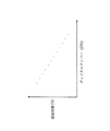
図4Bは、本発明の実施形態に係る、制御電圧VCと遅延時間τの関係図である。一般的に、制御電圧VCが上昇した場合、遅延時間τは、短縮される。いくつかの実施形態では、遅延時間τは、制御電圧VCと反比例する(例えば、τ* VC=k1、その中のk1は定数値である)が、この関係は、これらに限定されるものではない。いくつかの実施形態では、初期のホールドタイムは、可能な限り短く設定され、補正パルス信号CPの指示に対応して、徐々に長くなり、最適化した長さに達する。 FIG. 4B is a relationship diagram between the control voltage VC and the delay time τ according to the embodiment of the present invention. Generally, when the control voltage VC increases, the delay time τ is shortened. In some embodiments, the delay time τ is inversely proportional to the control voltage VC (eg, τ * VC = k1, where k1 is a constant value), but this relationship is not limited thereto. Absent. In some embodiments, the initial hold time is set as short as possible, and gradually increases and reaches an optimized length in response to an indication of the correction pulse signal CP.
図5Aは、本発明の実施形態に係る、遅延制御回路570の概略図である。図5Aの実施形態では、遅延制御回路570は、カウンタ571およびデジタル制御遅延(DCD)回路576を含む。カウンタ571は、複数ビットによって表されることがある、ディジタルナンバーDNを数える。回路576は、クロック信号CLKを遅延時間τ、遅延させて、遅延クロック信号CLKDを発生させることができる。DCD回路576は、当技術分野で周知のデジタル制御遅延回路で実施され得る。DCD回路576の遅延時間τは、ディジタルナンバーDNによって決まる。ディジタルナンバーDNは、補正パルス信号CPによってさらに調整される。いくつかの実施形態では、遅延制御回路570は、以下のように動作される。カウンタ571が高論理レベルと等しい補正パルス信号CPを受信する毎に、カウンタ571は、ディジタルナンバーDNを1増加させる。それとは反対に、カウンタ571が低論理レベルと等しい補正パルス信号CPを受信する毎に、カウンタ571は、ディジタルナンバーDNを変えずに維持される。
FIG. 5A is a schematic diagram of a
図5Bは、本発明の実施形態に係る、ディジタルナンバー(digital number)と遅延時間の関係図である。一般的に、ディジタルナンバーDNが増加された場合、遅延時間τは、短縮される。いくつかの実施形態では、遅延時間τは、ディジタルナンバーDNと反比例する(例えば、τ* DN=k2、その中のk2は定数値である)が、この関係は、これらに限定されるものではない。いくつかの実施形態では、初期のホールドタイムは、可能な限り短く設定され、補正パルス信号CPの指示に対応して、徐々に長くなり、最適化した長さに達する。 FIG. 5B is a relationship diagram between a digital number and a delay time according to an embodiment of the present invention. Generally, when the digital number DN is increased, the delay time τ is shortened. In some embodiments, the delay time τ is inversely proportional to the digital number DN (eg, τ * DN = k2, where k2 is a constant value), but this relationship is not limited thereto. Absent. In some embodiments, the initial hold time is set as short as possible, and gradually increases and reaches an optimized length in response to an indication of the correction pulse signal CP.
図6は、本発明の実施形態に係る、ホールドタイム最適化回路100を含む受信機600の概略図である。図6の実施形態では、受信機600は、データ遅延回路682、ホールドタイム最適化回路100、およびDフリップフロップ684を含む。データ遅延回路682は、データ信号DAを一定の遅延時間、遅延させて、遅延データ信号DADを発生させる。図1の実施形態に述べられたように、ホールドタイム最適化回路100は、補正回路110と遅延制御回路170を含む。遅延制御回路170は、クロック信号CLKを遅延時間τ、遅延させて、遅延クロック信号CLKDを発生させる。補正回路110は、遅延データ信号DADと遅延クロック信号CLKDに対応して補正パルス信号CPを発生させる。Dフリップフロップ684は、遅延データ信号DADを受信するデータ端子、遅延クロック信号CLKDを受信するクロック端子、およびサンプリング信号SAを出力する出力端子を有する。Dフリップフロップ684は、遅延クロック信号CLKDと遅延データ信号DADに対応してデータサンプリングプロセスを行うように用いられることができる。例えば、Dフリップフロップ684は、遅延データ信号DADを遅延クロック信号CLKDの各立ち上がりエッジでサンプリングすることができる。図6の実施形態では、遅延制御回路170の遅延時間τは、補正パルス信号CPに対応して最適化される。このようなフィードバック経路を用いることによって、遅延クロック信号CLKDと遅延データ信号DAD間のホールドタイムは、微調整される。ホールドタイム最適化回路100の詳細の構造と動作は、図1〜図5Bの実施形態に述べられた構造と動作とほぼ同じである。図1〜図5Bの実施形態と唯一異なることは、データ信号DAは、図6の実施形態のホールドタイム最適化回路100に印加される遅延データ信号DADと置き換えられることである。
FIG. 6 is a schematic diagram of a
図7Aは、本発明の実施形態に係る、受信機600の信号波形の概略図である。図7Aの実施形態では、遅延クロック信号CLKDと遅延データ信号DAD間のホールドタイムが微調整される前に、遅延クロック信号CLKDの立ち下がりエッジは、遅延データ信号DADの不正確な周期と揃えることができる。例えば、図7Aに示されるように、ホールドタイムは、負値である。即ち、遅延データ信号DADは、遅延クロック信号CLKDの各立ち上がりエッジの前に、その状態を変え、Dフリップフロップ684のサンプリング信号SAが誤った時間にサンプリングされた誤ったサンプリングデータを含むことになる。この場合、補正回路110の補正パルス信号CPは、多くの高いロジック間隔を含んで、現在のホールドタイムが許容できない(例えば、ホールドタイムが不十分である)ことを示す。
FIG. 7A is a schematic diagram of signal waveforms of a
図7Bは、本発明の実施形態に係る、受信機600の信号波形の概略図である。図7Bの実施形態では、遅延クロック信号CLKDと遅延データ信号DAD間のホールドタイムTHが微調整された後に、遅延クロック信号CLKDの立ち上がりエッジは、遅延データ信号DADの正確な周期内で揃えなければならない。例えば、図7Bに示されるように、微調整されたホールドタイムTHは、正値で十分であり、遅延データ信号DADは、遅延クロック信号CLKDの各立ち上がりエッジの後でホールドタイムTHの満了時に、その状態を変え、Dフリップフロップ684のサンプリング信号SAが正確なサンプリングデータのみを含むことになる。この場合、補正回路110の補正パルス信号CPは、低いロジックレベルを維持して、現在のホールドタイムが許容できることを示す。
FIG. 7B is a schematic diagram of signal waveforms of the
本発明のホールドタイム最適化回路100は、種々のデジタル回路の応用に適合する。本発明のホールドタイム最適化回路100は、プロセス、電圧、および温度(PVT)変動の影響を受けず、異なる環境で安定した性能を提供することができる。本発明は、デジタル回路のホールドタイムの長さを最適化するのに用いられることができ、データサンプリングプロセスの信頼度を向上させる利点を有する。
The hold
本発明は、単に図1〜図7Bの任意の1つまたは複数の実施形態の任意の1つまたは複数の特徴を含んでいるだけで、言い換えれば、全ての図に示されている特徴が本発明のホールドタイム最適化回路および受信機に実現されなければならないということではない。 The present invention merely includes any one or more features of any one or more embodiments of FIGS. 1-7B, in other words, the features shown in all figures are This is not to be realized in the hold time optimization circuit and receiver of the invention.
明細書における「第1の」、「第2の」、「第3の」等の序数詞の使用は、それ自体が優先度、序列、又は順序を示唆するものではなく、むしろ、単に2つ以上の特徴、要素、項目等を区別するためのラベルとして使用している。クレーム要素を変えるための、請求項における「第1の」、「第2の」、「第3の」等の序数詞の使用は、それ自体が、1つのクレーム要素を他のクレーム要素と比較して優先度、序列、又は順序、もしくは方法を実施する行為の時間的順序を示唆するものではなく、むしろ、単にクレーム要素を区別するために、特定の名前を有する1つのクレーム要素を同じ名前を有する他の要素から区別するためのラベルとして(だけ、序数詞を)使用している。 The use of ordinal numbers such as “first”, “second”, “third”, etc. in the specification does not imply a priority, order, or order per se, but rather just two or more. It is used as a label to distinguish features, elements, items, etc. The use of ordinal numbers such as “first”, “second”, “third”, etc. in a claim to change a claim element itself compares one claim element with another claim element. Does not imply priority, order, or order, or time order of actions to perform the method, but rather, simply distinguish one claim element with a particular name to distinguish the claim elements. It is used as a label (and only an ordinal) to distinguish it from other elements it has.
以上、実施例を示して本発明を説明しているが、当業者は、本発明の思想と技術的範囲から逸脱しない種々の修正及び変更を行い得る。実施形態および実施例は、例示的なものであるに過ぎず、本発明の範囲は、以下の請求項及びその均等のものによって規定されて保護される。 Although the present invention has been described with reference to the embodiments, those skilled in the art can make various modifications and changes without departing from the spirit and technical scope of the present invention. The embodiments and examples are illustrative only, and the scope of the present invention is defined and protected by the following claims and their equivalents.
100 ホールドタイム最適化回路
110、210、310 補正回路
170、470、570 遅延制御回路
220、221、229 グリッチ発生回路
231 立ち上がりエッジ検出器
232 立ち下がりエッジ検出器
241 第1のインバータ
242 第2のインバータ
243 第3のインバータ
251 第1のANDゲート
252 第2のANDゲート
261 第1のORゲート
262 第2のORゲート
263 NORゲート
471 第1のスイッチ
472 第2のスイッチ
473 電流源
474 直流(DC)電圧源
475 コンデンサ
476 電圧制御遅延(VCD)回路
571 カウンタ
576 デジタル制御遅延(DCD)回路
600 受信機
682 データ遅延回路
684 Dフリップフロップ
CLK クロック信号
CLKD 遅延クロック信号
CP 補正パルス信号
DA データ信号
DAD 遅延データ信号
DA〜B0、DA〜B1、DA〜B9 ビット
NC 制御ノード
SA サンプリング信号
TH ホールドタイム
VC 制御電圧
VSS 接地電圧
τ 遅延時間
100 Hold
Claims (8)
前記遅延クロック信号に対応してサンプリングされたデータ信号の遷移エッジと前記遅延クロック信号の遷移エッジに対応して前記補正パルス信号を発生させる補正回路を含み、
前記データ信号は、ビットを含み、且つ、前記補正回路は、グリッチ発生回路を含んでおり、
更に、前記グリッチ発生回路は、
前記ビットの立ち上がりエッジに対応して第1の検出信号を発生させる立ち上がりエッジ検出器、
前記ビットの立ち下がりエッジに対応して第2の検出信号を発生させる立ち下がりエッジ検出器、
前記第1の検出信号を受信する第1の入力端子、前記遅延クロック信号を受信する第2の入力端子、および出力端子を有する第1のANDゲート、
前記第2の検出信号を受信する第1の入力端子、前記遅延データ信号を受信する第2の入力端子、および出力端子を有する第2のANDゲート、ならびに
前記第1のANDゲートの前記出力端子に接続された第1の入力端子、前記第2のANDゲートの出力端子に接続された第2の入力端子、および補正パルス信号を出力する出力端子を有する第1のORゲートを含むホールドタイム最適化回路。 A delay control circuit that delays a clock signal to generate a delayed clock signal by adjusting a delay time adjusted according to the correction pulse signal; and a transition edge and the delay of the data signal sampled corresponding to the delayed clock signal in response to a transition edge of the clock signal observed including a correction circuit for generating the correction pulse signals,
The data signal includes a bit, and the correction circuit includes a glitch generation circuit,
Furthermore, the glitch generation circuit includes:
A rising edge detector for generating a first detection signal corresponding to the rising edge of the bit;
A falling edge detector for generating a second detection signal in response to a falling edge of the bit;
A first AND gate having a first input terminal for receiving the first detection signal, a second input terminal for receiving the delayed clock signal, and an output terminal;
A first input terminal for receiving the second detection signal, a second input terminal for receiving the delayed data signal, and a second AND gate having an output terminal; and
A first input terminal connected to the output terminal of the first AND gate; a second input terminal connected to the output terminal of the second AND gate; and an output terminal for outputting a correction pulse signal. the first OR gates including hold time optimization circuit.
前記ビットを受信する入力端子、および出力端子を有する第2のインバータ、ならびに
前記ビットを受信する第1の入力端子、前記第2のインバータの前記出力端子に接続された第2の入力端子、および前記第1の検出信号を出力する出力端子を有する第3のANDゲートを含む請求項1に記載のホールドタイム最適化回路。 The rising edge detector is
A second inverter having an input terminal for receiving the bit and an output terminal; a first input terminal for receiving the bit; a second input terminal connected to the output terminal of the second inverter; The hold time optimization circuit according to claim 1 , further comprising a third AND gate having an output terminal for outputting the first detection signal.
前記ビットを受信する入力端子、および出力端子を有する第3のインバータ、ならびに
前記ビットを受信する第1の入力端子、前記第3のインバータの出力端子に接続された第2の入力端子、および前記第2の検出信号を出力する出力端子を有するNORゲートを含む請求項1に記載のホールドタイム最適化回路。 The falling edge detector
A third inverter having an input terminal for receiving the bit and an output terminal; a first input terminal for receiving the bit; a second input terminal connected to the output terminal of the third inverter; The hold time optimizing circuit according to claim 1 , further comprising a NOR gate having an output terminal for outputting the second detection signal.
前記遅延クロック信号に対応してサンプリングされたデータ信号の遷移エッジと前記遅延クロック信号の遷移エッジに対応して前記補正パルス信号を発生させる補正回路を含み、
前記データ信号は、前記遅延クロック信号によってサンプリングされ、且つ、前記補正回路は、複数のグリッチ発生回路を含んでおり、
前記各グリッチ発生回路は、
各ビットの立ち上がりエッジに対応して第1の検出信号を発生させる立ち上がりエッジ検出器、
前記各ビットの立ち下がりエッジに対応して第2の検出信号を発生させる立ち下がりエッジ検出器、
前記第1の検出信号を受信する第1の入力端子、前記遅延クロック信号を受信する第2の入力端子、および出力端子を有する第1のANDゲート、
前記第2の検出信号を受信する第1の入力端子、前記遅延データ信号を受信する第2の入力端子、および出力端子を有する第2のANDゲート、ならびに
前記第1のANDゲートの前記出力端子に接続された第1の入力端子、前記第2のANDゲートの出力端子に接続された第2の入力端子、および出力端子を有する第1のORゲートを含むホールドタイム最適化回路。 A delay control circuit that delays the clock signal in response to the correction pulse signal, delays the clock signal, and generates a delayed clock signal; and
A correction circuit for generating the correction pulse signal corresponding to the transition edge of the delayed clock signal and the transition edge of the data signal sampled corresponding to the delayed clock signal ;
The data signal is sampled by the delayed clock signal, and the correction circuit includes a plurality of glitch generation circuits,
Each of the glitch generation circuits is
A rising edge detector for generating a first detection signal corresponding to the rising edge of each bit;
A falling edge detector for generating a second detection signal corresponding to the falling edge of each bit;
A first AND gate having a first input terminal for receiving the first detection signal, a second input terminal for receiving the delayed clock signal, and an output terminal;
A first input terminal for receiving the second detection signal; a second input terminal for receiving the delayed data signal; and a second AND gate having an output terminal; and the output terminal of the first AND gate. A hold time optimizing circuit including a first OR terminal having a first input terminal connected to the second input terminal, a second input terminal connected to the output terminal of the second AND gate, and an output terminal.
前記補正パルス信号を出力する出力端子を有する請求項4に記載のホールドタイム最適化回路。 The correction circuit further includes a second OR gate, and the second OR gate has a plurality of input terminals respectively connected to the output terminals of all the first OR gates of the glitch generation circuit, and The hold time optimizing circuit according to claim 4 , further comprising an output terminal that outputs the correction pulse signal.
制御ノードに接続された第1の端子、および直流(DC)電圧源に接続された第2の端子を有する第1のスイッチ、
電流源に接続された第1の端子、および前記制御ノードに接続された第2の端子を有する第2のスイッチ、
前記制御ノードに接続された第1の端子、および接地電圧に接続された第2の端子を有するコンデンサ、ならびに
前記クロック信号を制御ノードの制御電圧によって決まる前記遅延時間、遅延させて、前記遅延クロック信号を発生させる電圧制御遅延(VCD)回路を含む請求項1に記載のホールドタイム最適化回路。 The delay control circuit includes:
A first switch having a first terminal connected to the control node and a second terminal connected to a direct current (DC) voltage source;
A second switch having a first terminal connected to a current source and a second terminal connected to the control node;
A capacitor having a first terminal connected to the control node and a second terminal connected to a ground voltage; and delaying the clock signal for the delay time determined by the control voltage of the control node, and The hold time optimization circuit of claim 1 including a voltage controlled delay (VCD) circuit for generating a signal.
ディジタルナンバーを数え、高論理レベルと等しい前記補正パルス信号を受信する毎に、前記ディジタルナンバーを増加させるカウンタ、および
前記クロック信号を前記ディジタルナンバーによって決まる前記遅延時間、遅延させて、前記遅延クロック信号を発生させるデジタル制御遅延(DCD)回路を含む請求項1に記載のホールドタイム最適化回路。 The delay control circuit includes:
A counter that increments the digital number each time the digital pulse is counted and the correction pulse signal equal to a high logic level is received; and the delayed clock signal by delaying the clock signal by the delay time determined by the digital number The hold time optimization circuit of claim 1, comprising a digitally controlled delay (DCD) circuit for generating
Applications Claiming Priority (2)
| Application Number | Priority Date | Filing Date | Title |
|---|---|---|---|
| US14/306,567 US9337817B2 (en) | 2014-06-17 | 2014-06-17 | Hold-time optimization circuit and receiver with the same |
| US14/306,567 | 2014-06-17 |
Publications (2)
| Publication Number | Publication Date |
|---|---|
| JP2016005267A JP2016005267A (en) | 2016-01-12 |
| JP5945582B2 true JP5945582B2 (en) | 2016-07-05 |
Family
ID=51900212
Family Applications (1)
| Application Number | Title | Priority Date | Filing Date |
|---|---|---|---|
| JP2014231265A Active JP5945582B2 (en) | 2014-06-17 | 2014-11-14 | HOLD TIME OPTIMIZING CIRCUIT AND ITS RECEIVER |
Country Status (4)
| Country | Link |
|---|---|
| US (1) | US9337817B2 (en) |
| EP (1) | EP2958263B1 (en) |
| JP (1) | JP5945582B2 (en) |
| CN (2) | CN104363008B (en) |
Families Citing this family (6)
| Publication number | Priority date | Publication date | Assignee | Title |
|---|---|---|---|---|
| CN105512069B (en) * | 2015-12-04 | 2018-06-22 | 上海兆芯集成电路有限公司 | Deserializer device and its asynchronous conversion method |
| DE102016215570A1 (en) * | 2016-08-19 | 2018-02-22 | Ifm Electronic Gmbh | Evaluation circuit for a capacitive sensor, capacitive sensor and actuator in a motor vehicle |
| US10129012B2 (en) * | 2016-09-19 | 2018-11-13 | Sandisk Technologies Llc | Tuning circuitry and operations for non-source-synchronous systems |
| US9973178B1 (en) * | 2017-02-16 | 2018-05-15 | Nuvoton Technology Corporation | Method and apparatus for clock frequency multiplier |
| CN110867199B (en) * | 2018-08-27 | 2021-07-09 | 华邦电子股份有限公司 | Synchronous mirror delay circuit and synchronous mirror delay operation method |
| CN111398775B (en) * | 2019-01-03 | 2024-02-06 | 瑞昱半导体股份有限公司 | Circuit operation speed detection circuit |
Family Cites Families (17)
| Publication number | Priority date | Publication date | Assignee | Title |
|---|---|---|---|---|
| US5815017A (en) * | 1997-03-03 | 1998-09-29 | Motorola, Inc. | Forced oscillator circuit and method |
| US6247138B1 (en) | 1997-06-12 | 2001-06-12 | Fujitsu Limited | Timing signal generating circuit, semiconductor integrated circuit device and semiconductor integrated circuit system to which the timing signal generating circuit is applied, and signal transmission system |
| JP3512151B2 (en) * | 1997-09-29 | 2004-03-29 | 松下電器産業株式会社 | Skew correction device |
| JPH11122229A (en) | 1997-10-17 | 1999-04-30 | Fujitsu Ltd | Retiming circuit and retiming method |
| JP3908356B2 (en) | 1997-10-20 | 2007-04-25 | 富士通株式会社 | Semiconductor integrated circuit |
| JP3745517B2 (en) * | 1997-10-20 | 2006-02-15 | 富士通株式会社 | Timing circuit |
| JP2003058273A (en) * | 2001-08-13 | 2003-02-28 | Oki Electric Ind Co Ltd | Hold time measuring circuit |
| US6895540B2 (en) * | 2002-07-18 | 2005-05-17 | Faraday Technology Corp. | Mux scan cell with delay circuit for reducing hold-time violations |
| US7084679B2 (en) * | 2004-04-15 | 2006-08-01 | International Business Machines Corporation | Method and apparatus for ensuring synchronization of clocks in a multiple clock system |
| JP4117330B2 (en) * | 2004-05-26 | 2008-07-16 | 松下電器産業株式会社 | Skew correction device |
| JP4667196B2 (en) * | 2005-10-12 | 2011-04-06 | パナソニック株式会社 | Phase adjustment circuit |
| JP4795032B2 (en) | 2006-01-30 | 2011-10-19 | エルピーダメモリ株式会社 | Timing adjustment circuit and semiconductor device |
| JP2007208774A (en) | 2006-02-03 | 2007-08-16 | Yokogawa Electric Corp | Phase control circuit |
| JP4701102B2 (en) * | 2006-02-17 | 2011-06-15 | パナソニック株式会社 | Timing correction device |
| TWI368837B (en) * | 2008-07-16 | 2012-07-21 | Acbel Polytech Inc | Ac to dc power converter with hold up time function |
| JP5397025B2 (en) * | 2009-06-02 | 2014-01-22 | ソニー株式会社 | Clock reproduction device and electronic device |
| JP5776657B2 (en) * | 2012-09-18 | 2015-09-09 | 株式会社デンソー | Receiver circuit |
-
2014
- 2014-06-17 US US14/306,567 patent/US9337817B2/en active Active
- 2014-11-07 CN CN201410687616.0A patent/CN104363008B/en active Active
- 2014-11-07 CN CN201410625422.8A patent/CN104333357B/en active Active
- 2014-11-12 EP EP14192781.4A patent/EP2958263B1/en active Active
- 2014-11-14 JP JP2014231265A patent/JP5945582B2/en active Active
Also Published As
| Publication number | Publication date |
|---|---|
| EP2958263A1 (en) | 2015-12-23 |
| US9337817B2 (en) | 2016-05-10 |
| CN104333357A (en) | 2015-02-04 |
| CN104363008B (en) | 2017-06-13 |
| CN104333357B (en) | 2017-04-05 |
| JP2016005267A (en) | 2016-01-12 |
| EP2958263B1 (en) | 2018-08-08 |
| CN104363008A (en) | 2015-02-18 |
| US20150365081A1 (en) | 2015-12-17 |
Similar Documents
| Publication | Publication Date | Title |
|---|---|---|
| JP5945582B2 (en) | HOLD TIME OPTIMIZING CIRCUIT AND ITS RECEIVER | |
| US7602224B2 (en) | Semiconductor device having delay locked loop and method for driving the same | |
| US8004337B2 (en) | Digital delay circuit | |
| US9054681B2 (en) | High speed duty cycle correction and double to single ended conversion circuit for PLL | |
| EP0584946A2 (en) | Logic interface circuits | |
| US8255748B2 (en) | Soft error and transient error detection device and methods therefor | |
| US20090058483A1 (en) | Duty cycle correcting circuit and method | |
| US9537490B2 (en) | Duty cycle detection circuit and semiconductor apparatus including the same | |
| JP2011055048A (en) | Polyphase clock generating circuit | |
| WO2007150056A2 (en) | Method and delay circuit with accurately controlled duty cycle | |
| JP2004242317A (en) | Frequency multiplier and multiplication method for adjusting duty cycle of clock | |
| US9118308B1 (en) | Duty cycle corrector | |
| US20170063363A1 (en) | Comparator, electronic circuit, and method of controlling comparator | |
| KR100843002B1 (en) | duty cycle correction circuit and delay locked loop with the same | |
| US20140092951A1 (en) | Jitter Tolerant Receiver | |
| CN107046416B (en) | Duty ratio correction circuit | |
| US20080186075A1 (en) | Level shifter of semiconductor device and method for controlling duty ratio in the device | |
| CN107872208B (en) | Clock signal loss detection device | |
| KR20200145266A (en) | Phase detection circuit, clock generation circuit and semiconductor apparatus using the same | |
| KR100609755B1 (en) | Phase detector and delay locked loop comprising the same | |
| US10110214B2 (en) | Voltage comparator circuit including a plurality of voltage controlled delay lines | |
| EP2884366A1 (en) | Self-adjusting delay circuit | |
| US8270557B2 (en) | Integrated circuit and method for driving the same | |
| US6194926B1 (en) | Operation timing controllable system | |
| US6768347B2 (en) | Precise phase detector |
Legal Events
| Date | Code | Title | Description |
|---|---|---|---|
| RD04 | Notification of resignation of power of attorney |
Free format text: JAPANESE INTERMEDIATE CODE: A7424 Effective date: 20151127 |
|
| A131 | Notification of reasons for refusal |
Free format text: JAPANESE INTERMEDIATE CODE: A131 Effective date: 20160210 |
|
| A521 | Request for written amendment filed |
Free format text: JAPANESE INTERMEDIATE CODE: A523 Effective date: 20160419 |
|
| TRDD | Decision of grant or rejection written | ||
| A01 | Written decision to grant a patent or to grant a registration (utility model) |
Free format text: JAPANESE INTERMEDIATE CODE: A01 Effective date: 20160511 |
|
| A61 | First payment of annual fees (during grant procedure) |
Free format text: JAPANESE INTERMEDIATE CODE: A61 Effective date: 20160530 |
|
| R150 | Certificate of patent or registration of utility model |
Ref document number: 5945582 Country of ref document: JP Free format text: JAPANESE INTERMEDIATE CODE: R150 |
|
| R250 | Receipt of annual fees |
Free format text: JAPANESE INTERMEDIATE CODE: R250 |
|
| R250 | Receipt of annual fees |
Free format text: JAPANESE INTERMEDIATE CODE: R250 |
|
| R250 | Receipt of annual fees |
Free format text: JAPANESE INTERMEDIATE CODE: R250 |
|
| R250 | Receipt of annual fees |
Free format text: JAPANESE INTERMEDIATE CODE: R250 |
|
| R250 | Receipt of annual fees |
Free format text: JAPANESE INTERMEDIATE CODE: R250 |