JP5932249B2 - Image forming apparatus - Google Patents
Image forming apparatus Download PDFInfo
- Publication number
- JP5932249B2 JP5932249B2 JP2011132533A JP2011132533A JP5932249B2 JP 5932249 B2 JP5932249 B2 JP 5932249B2 JP 2011132533 A JP2011132533 A JP 2011132533A JP 2011132533 A JP2011132533 A JP 2011132533A JP 5932249 B2 JP5932249 B2 JP 5932249B2
- Authority
- JP
- Japan
- Prior art keywords
- power
- state
- switch
- capacitor
- power supply
- Prior art date
- Legal status (The legal status is an assumption and is not a legal conclusion. Google has not performed a legal analysis and makes no representation as to the accuracy of the status listed.)
- Expired - Fee Related
Links
- 239000003990 capacitor Substances 0.000 claims description 101
- 238000012360 testing method Methods 0.000 claims description 15
- 238000001514 detection method Methods 0.000 claims description 7
- 238000007599 discharging Methods 0.000 claims description 6
- 238000009499 grossing Methods 0.000 claims description 4
- 230000004044 response Effects 0.000 claims description 4
- 238000010586 diagram Methods 0.000 description 23
- 239000000758 substrate Substances 0.000 description 11
- 230000015572 biosynthetic process Effects 0.000 description 7
- 238000007600 charging Methods 0.000 description 6
- 239000004973 liquid crystal related substance Substances 0.000 description 6
- 238000000034 method Methods 0.000 description 6
- 230000006378 damage Effects 0.000 description 4
- 238000012423 maintenance Methods 0.000 description 4
- 238000012546 transfer Methods 0.000 description 4
- 238000006243 chemical reaction Methods 0.000 description 3
- 238000003780 insertion Methods 0.000 description 3
- 230000037431 insertion Effects 0.000 description 3
- 239000004065 semiconductor Substances 0.000 description 3
- 230000006870 function Effects 0.000 description 2
- 230000001681 protective effect Effects 0.000 description 2
- 230000004397 blinking Effects 0.000 description 1
- 239000000470 constituent Substances 0.000 description 1
- 238000011161 development Methods 0.000 description 1
- 238000000605 extraction Methods 0.000 description 1
- 238000009434 installation Methods 0.000 description 1
- 230000003287 optical effect Effects 0.000 description 1
- 238000012545 processing Methods 0.000 description 1
Images


Classifications
-
- G—PHYSICS
- G03—PHOTOGRAPHY; CINEMATOGRAPHY; ANALOGOUS TECHNIQUES USING WAVES OTHER THAN OPTICAL WAVES; ELECTROGRAPHY; HOLOGRAPHY
- G03G—ELECTROGRAPHY; ELECTROPHOTOGRAPHY; MAGNETOGRAPHY
- G03G15/00—Apparatus for electrographic processes using a charge pattern
- G03G15/80—Details relating to power supplies, circuits boards, electrical connections
Description
本発明は、画像形成装置に関し、特にコンデンサ放電制御を有する画像形成装置に関する。 The present invention relates to an image forming apparatus, and more particularly to an image forming apparatus having capacitor discharge control.
コンデンサを備えた基板を有する画像形成装置において、メンテナンス作業などで基板の挿抜を行う際、コンデンサに充電された電荷による活線挿抜によって、挿抜する基板が破壊されることを防止する必要がある。そして、この防止のために、コンデンサの放電に関連して幾つかの提案がなされている。 In an image forming apparatus having a substrate provided with a capacitor, when the substrate is inserted / removed for maintenance work or the like, it is necessary to prevent the inserted / removed substrate from being destroyed by hot-line insertion / removal due to the electric charge charged in the capacitor. In order to prevent this, several proposals have been made in relation to capacitor discharge.
例えば、特許文献1には、コンデンサにチャージした電荷の放電により発光するフラッシュランプと、電源がオフになったことを検出するパワーオフ検出回路と、パワーオフを検出すると強制的にコンデンサを放電させるフラッシュランプ用電源が開示されている。 For example, Patent Document 1 discloses a flash lamp that emits light by discharging electric charges charged in a capacitor, a power-off detection circuit that detects that the power is turned off, and a capacitor that is forcibly discharged when power-off is detected. A power supply for a flash lamp is disclosed.
また、特許文献2には、保護カバーと、保護カバーの設置状態を検出するスイッチを含む緊急放電回路とを備え、カバーが取り外されていることを検出すると、コンデンサに蓄えられた電荷を放電する画像形成装置が開示されている。 Further, Patent Document 2 includes a protective cover and an emergency discharge circuit including a switch for detecting the installation state of the protective cover, and when it is detected that the cover is removed, the electric charge stored in the capacitor is discharged. An image forming apparatus is disclosed.
近年、益々の省電力化が促進されており。例えば1.0Wの待機電力で待機動作を行うプリンタが提案されている。そして、このような低消費電力での待機動作が可能なプリンタにおいては、常夜電源が設けられている。この常夜電源は、ユーザ操作により装置本体の電源がOFF状態に設定されたとしても、例えばプリンタへの外部装置からのアクセスを検知する為に設けられている。これにより、ユーザが利用したいときにプリンタの電源をOFF状態から自動的に復帰させることができる。 In recent years, more and more power saving has been promoted. For example, a printer that performs a standby operation with a standby power of 1.0 W has been proposed. In such a printer capable of standby operation with low power consumption, a power source is provided all night. Even if the power supply of the apparatus main body is set to the OFF state by the user operation, this night power supply is provided, for example, to detect access from the external apparatus to the printer. Thus, when the user wants to use the printer, the printer power can be automatically restored from the OFF state.
ここで、常夜電源についてもう少し詳しく説明する。常夜電源は、平滑化された電源出力を生成するべくンデンサを通常備えており、そのコンデンサを常時充電(電荷蓄積)しながら、上述した待機動作を行う。例えば1.0Wなどの低い消費電力で待機する場合には、極力コンデンサの充電について電力を消費しないようにしたい。従って、極力、コンデンサを放電しないように、その放電経路を遮断する施策が回路に施されている。これは、放電電流が大きいと、それを充電するように回路が作動してしまい、結果、待機電力が増加するからである。 Here, I will explain the nighttime power supply in a little more detail. The night-time power supply usually includes a capacitor to generate a smoothed power output, and performs the above-described standby operation while always charging (charging) the capacitor. For example, when waiting with a low power consumption of 1.0 W or the like, it is desirable to avoid consuming power for charging the capacitor as much as possible. Therefore, measures are taken in the circuit to cut off the discharge path so as not to discharge the capacitor as much as possible. This is because if the discharge current is large, the circuit operates so as to charge it, resulting in an increase in standby power.
このように、近年においては、プリンタの待機動作における低消費電力ばかりでなく、待機動作から自動復帰できるなどのユーザビリティーを向上させることも求められている。これに対して、先に説明した特許文献1、2のように自動的且つ即時にコンデンサの電荷を放電する手法では、メンテナンス性を向上させることはできるものの、ユーザビリティーの向上については十分に対応することができない。 As described above, in recent years, not only low power consumption in the standby operation of the printer but also improvement in usability such as being able to automatically return from the standby operation is required. On the other hand, the method of automatically and immediately discharging the capacitor charge as described in Patent Documents 1 and 2 described above can improve the maintainability, but sufficiently cope with the improvement of usability. Can not do it.
一方において、上で説明したように、メンテナンス作業などで基板の挿抜を行う際において、コンデンサに充電された電荷による活線挿抜によって、挿抜する基板が破壊されることを防止するべく、コンデンサを放電する必要がある。しかし、先に説明したようなコンデンサを含む常夜電源を備えたプリンタにおいては、即座且つ自動的にコンデンサの電荷を放電するわけにはいかず、サービスマンはコンデンサの電荷を放電する為に長時間待たされることになる。 On the other hand, as described above, when inserting / removing a substrate for maintenance work or the like, the capacitor is discharged in order to prevent destruction of the substrate to be inserted / removed by hot-line insertion / removal due to the charge charged in the capacitor. There is a need to. However, in a printer equipped with an overnight power source including a capacitor as described above, the capacitor charge cannot be discharged immediately and automatically, and a service person cannot wait for a long time to discharge the capacitor charge. I will be waiting.
ここで、この問題に対し、ACインレットから電源ケーブルを抜いたことを検知し、コンデンサの電荷を自動放電に移行させるような回路をプリンタに設ける解決策も考えられる。しかし、この解決策では、ACインレットからの電源ケーブル抜けの自動検知回路を新たに設ける必要があり、コストアップを引き起こしてしまう。また、例えば1.0Wの待機電力で待機している間にも、ゼロクロス検知を利用した自動検知回路を動作させる必要があり、フォトカプラなどの動作電力が増加してしまう。或いは、停電時や電源遮断時のときにデータ退避を行うべく、コンデンサに充電された電荷を利用し、メモリのリード・ライトを行うような形態も想定される。しかし、このような想定の場合に、特許文献1、2の開示の如く、即座にコンデンサの電荷を放電してしまうと、プリンタの動作に支障をきたしてしまう虞が出てくる。 Here, with respect to this problem, a solution is also conceivable in which the printer is provided with a circuit that detects that the power cable is disconnected from the AC inlet and shifts the capacitor charge to automatic discharge. However, in this solution, it is necessary to newly provide an automatic detection circuit for disconnecting the power cable from the AC inlet, which causes an increase in cost. Further, for example, it is necessary to operate an automatic detection circuit using zero-crossing detection while waiting at a standby power of 1.0 W, which increases the operating power of a photocoupler or the like. Alternatively, in order to save data at the time of a power failure or power cut-off, a form in which memory is read / written using the electric charge charged in the capacitor is also assumed. However, in such an assumption, if the capacitor charge is discharged immediately as disclosed in Patent Documents 1 and 2, there is a possibility that the operation of the printer may be hindered.
本発明は上記課題に鑑みてなされたものであり、ユーザビリティーを持たせた低消費電力のプリンタにおいて、コストを抑えつつ、コンデンサの放電を迅速に行えるプリンタを提供することを目的とする。 SUMMARY OF THE INVENTION The present invention has been made in view of the above problems, and an object of the present invention is to provide a low power consumption printer with usability that can quickly discharge a capacitor while suppressing cost.
本発明は上記課題に鑑みてなされたものであり、本発明における画像形成装置は、入力された交流電圧を変換し、変換した電圧を出力する電源と、前記電源の出力側とグランドの間に接続され、前記電源からの出力された電圧を平滑化するコンデンサと、前記画像形成装置のテストプリント動作を指示するための操作スイッチと、前記操作スイッチの操作を検出するための制御部と、前記制御部からの信号に応じて前記電源と発光部を接続した第1の状態と、前記電源と前記発光部が切断した第2の状態に切り換えるためのスイッチと、を有し、前記画像形成装置への電力供給状態として、前記スイッチを前記第1の状態に切り換えて前記発光部に電力を供給し、且つ、前記制御部に電力を供給した第1の電力供給状態と、前記スイッチを前記第二の状態に切り換えて、前記発光部への電力の供給を停止し、且つ、前記制御部に電力を供給した第2の電力供給状態を切り替え可能であって、前記第1の電力供給状態において、前記制御部により前記操作スイッチによる前記操作が検出されると、前記検出された前記操作に応じて前記テストプリント動作が行われ、前記第2の電力供給状態において、前記制御部により前記操作スイッチによる前記操作が検出されると、前記制御部は、前記スイッチにより前記電源と前記発光部が切断した状態から前記電源と前記発光部が接続された状態に切り替えて前記発光部を点灯させることにより、前記コンデンサを放電することを特徴とする。 The present invention has been made in view of the above problems, and an image forming apparatus according to the present invention converts an input AC voltage and outputs a converted voltage between an output side of the power supply and a ground. are connected, a capacitor for smoothing the output voltage from the power supply, and an operation switch for instructing the test print operation of the image forming apparatus, and a control unit for detecting an operation of the operation switch, the A first state in which the power source and the light emitting unit are connected in response to a signal from the control unit; and a switch for switching to a second state in which the power source and the light emitting unit are disconnected, and the image forming apparatus. as a power supply state to supplies power to the light emitting portion by switching the switch to the first state, and the first and the power supply while supplying power to the control unit, before the switch Switching to the second state, and stops the power supply to the light emitting portion, and, a switchable second power supply while supplying power to the control unit, said first power supply state in, when the operation by the operation switch is detected by the control unit, wherein the test printing operation in response to said detected operation is performed, in the second power supply state, the operation by the control unit When the operation by the switch is detected, the control unit switches the state where the power source and the light emitting unit are disconnected by the switch from the state where the power source and the light emitting unit are connected, and turns on the light emitting unit. To discharge the capacitor .
本発明によれば、ユーザビリティーを持たせた低消費電力のプリンタにおいて、コストを抑えつつ、コンデンサの放電を迅速に行えるプリンタを提供することができる。 According to the present invention, it is possible to provide a printer capable of quickly discharging a capacitor while suppressing cost in a low power consumption printer having usability.
以下に、図面を参照して、この発明の好適な実施の形態を例示的に詳しく説明する。ただし、この実施の形態に記載されている構成要素はあくまで例示であり、この発明の範囲をそれらのみに限定する趣旨のものではない。 Hereinafter, exemplary embodiments of the present invention will be described in detail with reference to the drawings. However, the constituent elements described in this embodiment are merely examples, and are not intended to limit the scope of the present invention only to them.
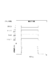
[画像形成装置の概略図]
図1は、本実施例の画像形成装置の全体構成を示す概略図である。図1において、100は画像形成装置本体である。101は、画像形成装置に着脱可能なトナーカートリッジ、102は像担持体である感光体である。103は光源としての半導体レーザ、105はスキャナモータ104にて回転するポリゴンミラー、106は半導体レーザ103から出射された光線がポリゴンミラー105によって偏光され、感光体102上を走査するレーザ光路である。107はポリゴンミラー105によって偏光された光線を受光する受光センサである。108は感光体102上を一様に帯電するための帯電ローラ、109は感光体102上に形成された静電潜像をトナーにて現像するための現像ローラである。110は現像ローラ109にて現像されたトナー像を所定の記録用紙に転写するための転写ローラである。111は定着器を示し、112は記録用紙に転写されたトナーを熱にて融着するための定着器の定着ヒータ、124定着フィルムと125加圧ローラにて記録用紙を搬送しながら記録用紙上のトナーを記録用紙に加熱加圧定着させる。113は用紙を格納する給紙カセットである。114は1回転して給紙カセット113から用紙を給紙し搬送路に送り出す給紙ローラである。フィードローラ115とリタードローラ116は給紙ローラ114にてピックアップされた用紙が用紙束である場合に用紙を1枚に分離して搬送路に送り出すためのローラ対である。117はカセットから給紙された用紙を画像形成部へ搬送するための中間ローラ、118は搬送された用紙を感光体102へ送り込む転写前ローラである。119は給紙された用紙に対し、感光体102への画像書き込み(記録/印字)と用紙搬送の同期を取るとともに給紙された用紙の搬送方向の長さを測定するためのトップセンサである。120は定着後の用紙の有無を検出するための定着センサ、121は定着後の用紙を排紙搬送路へ排出する搬送ローラ、122は排紙用紙を積載する排紙トレイ123へ用紙を排出する排紙ローラである。商用電源(商用交流電源)150はAC電圧を出力する。そして、電源ケーブル151を介して、商用電源(商用交流電源)150に接続された電源部208は、AC電圧を略直流の電圧に変換し、変換後の電圧を前述の画像形成動作で消費される電力を装置各部へ供給する。
[Schematic of image forming apparatus]
FIG. 1 is a schematic diagram illustrating the overall configuration of the image forming apparatus according to the present exemplary embodiment. In FIG. 1,
[画像形成装置のブロック図]
図2は、画像形成装置100における回路構成のブロック図である。図2において、201は不図示のホストコンピュータ等の外部機器から送られる画像コードデータをプリンタの印字に必要なビットデータに展開するとともに、プリンタ内部情報を読み取りそれを表示するためのプリンタコントローラである。202はプリンタエンジンの各部をプリンタコントローラ201の指示にしたがってプリント動作制御するとともに、プリンタコントローラ201へプリンタ内部情報を報知するためのエンジンコントローラである。エンジンコントローラ202は、CPUおよびASIC回路から構成される。203は帯電、現像、転写等の各高圧出力制御をエンジンコントローラ202の指示にしたがっておこなう高圧制御部である。204はスキャナモータ104の駆動/停止、レーザビームの点灯をエンジンコントローラ202の指示にしたがって制御する光学系制御部である。205は定着ヒータへの通電の駆動/停止をエンジンコントローラ202の指示にしたがって行う定着器制御部である。206は、受光センサ107、トップセンサ119、定着センサ120などの検出結果をエンジンコントローラ202へ報知するセンサ入力部である。207はエンジンコントローラ202の指示に従い、記録用紙搬送のためにモータ/ローラ等の駆動/停止を行う用紙搬送制御部である。用紙搬送制御部206は、図1の給紙ローラ114、フィードリタードローラ対115、116、転写前ローラ118、感光体102、定着フィルム124、加圧ローラ125、搬送ローラ121、排紙ローラ122の駆動/停止の制御を司る。208は、エンジンコントローラやプリンタコントローラ、各制御部に電源供給を行う電源部である。
[Block diagram of image forming apparatus]
FIG. 2 is a block diagram of a circuit configuration in the
電源部208は、電源ケーブル151が挿入されてAC入力が行われるとDC電圧を生成する。また電源部208は、ユーザによりプリンタの電源OFF操作がなされた場合でも、自動復帰動作が可能なように、第1の電力よりも供給量が小さい第2の電力の電源供給を継続する常夜電源を備えている。ここでの電源OFFでは、電源供給が全く遮断された状態を指すのではなく、電源ON状態への自動復帰の為に必要な最低限の電源供給が行われている。また、電源ONとは、電源OFF状態よりも多くの電力が供給された状態であって、外部装置より印刷データを受信し画像形成を開始できる状態に対応する。この電源ONの状態とはプリント待機状態に対応する。またこの電源ON状態では、エンジンコントローラ202、プリンタコントローラ201にも電力が供給されている。また電源ONの状態では、CPU306が動作クロック周波数が、電源OFF時クロック周波数よりも高く設定されている。
The
また、プリンタコントローラ201は、作業性向上のため、メンテナンスを行う作業者が容易に着脱できる構成となっている。作業者は、電源ケーブルを抜いてから着脱を行う。
Further, the
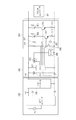
[電源回路図]
図3は、画像形成装置100におけるエンジンコントローラ202とプリンタコントローラ201、電源部208の回路構成図である。エンジンコントローラ202は、CPU306を有する。
[Power supply circuit diagram]
FIG. 3 is a circuit configuration diagram of the
電源部208にAC入力がなされると、AC/DCコンバータ301は、AC電流からDC電流に変換を行ってDC電圧(変換後電圧)を生成する。尚、不図示ではあるがAC/DCコンバータ301中には、出力電圧の平滑化の為のコンデンサが設けられている。生成されたDC電圧は、分圧抵抗(不図示)によって分圧され、分圧された電圧が所定電圧となるようにフィードバックされる。CPU306は、分圧抵抗を切り換えることによって出力電圧を切り替えることができる。分圧抵抗が、分圧抵抗1の場合には+V1(変換後電圧)を出力し、分圧抵抗2の場合には+V2(変換後電圧)を出力する。+V1と+V2の関係は、+V1>+V2である。AC/DCコンバータ301から出力される+V1は、DC/DCコンバータ305以外にも、V1供給用ロードスイッチ(不図示)を介して、半導体レーザ103を搭載したレーザ駆動基板(不図示)などにも供給される。
When AC input is made to the
DC/DCコンバータ305は、降圧型DC/DCコンバータであり、+V1が入力されると+V2を出力する。DC/DCコンバータ305によって生成された+V2は、エンジンコントローラ202、プリンタコントローラ201に供給される。CPU306、コンデンサ304、電流制限抵抗307、308、310、テストプリントを実行するためのSW302、ユーザがプリンタ状態を電源ONと電源OFFとの間で切り替えるためのSW303は、エンジンコントローラ内の+V2に接続されている。また、プリンタ状態が電源ONのときに発光してプリンタ状態が電源ONであることを報知するLED311(負荷としての装置外部から目視可能な表示手段)も、エンジンコントローラ内の+V2に接続されている。また、LED311の電源との接続状態、すなわちLED311のON(電源と負荷とを接続した状態)/OFF(電源と負荷とを切断した状態)を行うための駆動トランジスタであるTr309(スイッチ手段)も、エンジンコントローラ内の+V2に接続されている。ここで、コンデンサ304は、DC/DCコンバータ305とグランド間に接続されDC/DCコンバータ305からの出力電圧を平滑化する機能を担う。この平滑化後の出力電圧が装置本体に供給されることとなる。
The DC /
FET312(スイッチ手段)は、+V2からセンサ206(負荷)への電源供給をON(電源と負荷とを接続した状態)/OFF(電源と負荷とを切断した状態)するためのロードスイッチである。センサ206は、フォトインタラプタなどのセンサが複数個接続されており、電源供給すると一定電力を消費する。また、+V2は、V2供給用ロードスイッチ(不図示)を介して、その他のユニット(不図示)への電源供給を行っている。V1供給用ロードスイッチおよびV2供給用ロードスイッチは、CPU306からの指示によってON/OFFが行われる。
The FET 312 (switching means) is a load switch for turning ON the power supply from + V2 to the sensor 206 (load) (a state where the power source and the load are connected) / OFF (a state where the power source and the load are disconnected). The
SW302、SW303はモーメンタリスイッチであり、スイッチを押下している間だけスイッチ内の電極同士が接触して導通し、スイッチの押下を止めると、スイッチ内の電極同士が離間して非導通を維持する。CPU306は、電源ON時及びOFF時の双方において、各モーメンタリスイッチの押下状態を検出可能な状態で動作しており、また動作できるようにCPU306に電力供給が行われている。
SW302 and SW303 are momentary switches, and the electrodes in the switch come into contact with each other only while the switch is pressed, and when the switch is stopped, the electrodes in the switch are separated and maintain non-conduction. . The
プリンタコントローラ201は、プリンタ表面に配置された基板固定ネジ(不図示)を外すとことによってプリンタから基板を取り外せる構成となっている。SW302は、メンテナンス時の印刷動作確認のテストプリントを行うためのスイッチ(SW)であり、電源のON及びOFFの操作以外の操作を行う為の操作手段に相当する。通常、SW302に対応する操作部は、ユーザが操作しないようにプリンタの背面外装の内側等に構成されている。背面外装には、SW302と対面する位置に専用穴が設けられており、サービスマンは専用工具を使用することによって、プリンタ外装を外さずに前記SW302を押すことができる。
The
またプリンタコントローラ201は、装置本体が電源OFF状態においても、ホストコンピュータ等の外部機器からのアクセス(例えば印刷ジョブの投入)を検知する機能を備えている。そして、CPU306に検知した外部装置からのアクセスがあったことを通知する。CPU306は、電源OFF状態においても、外部からのアクセスを示す通知を検出可能なように動作している。
The
電源ケーブルが挿入されてAC入力が開始されると、プリンタ状態は電源OFF状態となる。電源OFF状態では、CPU306が動作クロック周波数を下げた低消費電力モードとなるとともにLED311は消灯状態となる。また、電力消費を小さくするため、CPU306によってFET312はOFFされ、センサ206への電源供給はOFFとなっている。また、CPU306によって、V1供給用ロードスイッチおよびV2供給用ロードスイッチがOFFとなり、その他のユニット(不図示)への電源供給がOFFとなっている。CPUによってAC/DCコンバータ301の分圧抵抗は分圧抵抗2に切り替えられ、AC/DCコンバータ301の出力電圧は、+V2となっている。
When the power cable is inserted and AC input is started, the printer state is turned off. In the power OFF state, the
DC/DCコンバータ305は、出力電圧が+V2となるようにフィードバックを行うため、出力電圧と同等の+V2が入力されると、フィードバックに使用する電流が小さくなり、ほとんど電流を消費しない。
Since the DC /
そして、SW303に対応する操作ボタンが押されると、プリンタ状態が電源OFF状態から電源ON状態となる。電源ON状態では、CPU306が通常の動作クロック周波数に復帰し、LED311(負荷)を点灯させる。また、CPU306からの指示によって、AC/DCコンバータ301の分圧抵抗は分圧抵抗1に切り替えられ、AC/DCコンバータ301の出力電圧が+V1となる。また、CPU306は、FET312をONしてセンサへの電源供給を開始するとともにV1供給用ロードスイッチおよびV2供給用ロードスイッチをONすることで、その他のユニットへの電源供給を開始する。電源ON状態でSW302が押されると、プリント動作を開始し、テストプリント画像が印刷される。尚、テストプリントとは、例えば、黒の横線をA4一頁にわたって形成したものであり、プリンタがトナー像を正常にできているか否かをサービスマンが確認する為のものである。勿論、テストプリントにおいて何を形成するかは、その用途に応じて適宜変更されるものであり、特に、ここで例示した形態に限定されるものではない。
When the operation button corresponding to
[コンデンサ放電制御のフローチャート]
図4は本実施例におけるコンデンサ放電制御のフローチャートを示す。尚、図4のフローチャートは、プリント待機時において行われるものであり、このとき定着器111等のトナー画像形成に直接的に係る部材にトナー像形成時における電力は供給されていない。逆に、図4のフローチャートにおいて電源に接続されている負荷は、プリント待機時にも電源が供給される負荷ということになる。
[Capacitor discharge control flowchart]
FIG. 4 shows a flowchart of capacitor discharge control in this embodiment. Note that the flowchart of FIG. 4 is performed during printing standby, and at this time, no power is supplied to the members directly related to toner image formation, such as the fixing
CPU306は、現在のプリンタ状態が電源ON状態か電源OFF状態かを判別する(S401)。ここで電源ON状態(第1の電力供給状態)においては、先に説明した、SW303や、SW302の押下状態を検知する少なくともCPU306(操作手段への操作を検出する検出手段として機能)に電源が供給されている。また、CPU306以外の負荷である少なくともセンサ206やLED311などにも電源が供給されている。また、レーザ駆動基板(不図示)などにも電源を供給してもよい。また、電源OFF状態(第2の電力状態)においては、電源ON状態において電力が供給されているセンサ206やLED311などの負荷への電力が遮断されている。つまりスイッチ(FET312など)により負荷と電源の接続が切断されている。また、電源OFF状態においては、操作部への操作や電源のON及びOFFの操作や外部装置からのアクセスを検出するCPU306やスイッチ手段のみに電源が供給されている。当然のことながら電源OFF状態における消費電力は電源ON状態のときのそれに比べて少ない。
The
CPU306が、プリンタ状態が電源ON状態であると判別すると、CPU306は、SW302(操作部)がONされているかを検出する(S407)。
When the
S407でCPU306によりSW302がONされたことが検出された場合には、S302の押下に応じた処理としてCPU306は画像形成部を制御しテストプリント画像の印刷を実行し(S408)、S401に戻る。SW302の押下状態がOFFの場合には、S401に戻る。
If the
S401で、CPU306により、プリンタ状態が電源OFF状態であると判別されると、CPU306は、SW302がONされているかを検出する(S402)。SW302がONされていることを検出した場合、Tr309(スイッチ手段)をONしてLED311(負荷)を点灯させる(S403)。また、FET312(スイッチ手段)をONしてセンサ206(負荷)を接続する(S404)。ここでTr309、FET321のONを継続する時間は、商用電源(商用交流電源)150からのAC入力電圧が遮断された状況下において少なくともコンデンサ304が放電を完了する為の時間以上の時間とする。
If the
一方、CPU306が、SW302のOFFを検出した場合、CPU306は、Tr309(スイッチ手段)をOFFして電源と切断状態にしLED311(負荷)を消灯させ(S405)電源と切断状態にする。また、FET312(スイッチ手段)をOFFしてセンサ206と電源の接続を切断し(S406)、S401に戻る。SW302のOFFを検出した場合で、既にLED311が消灯し、FET312がOFF状態であれば、その状態を維持して、S401に戻る。
On the other hand, when the
[コンデンサ放電制御におけるタイミングチャート]
次に本実施例におけるコンデンサ放電制御について説明する。図5は、コンデンサ放電制御におけるタイミングチャートを示す。図4のフローチャートにも対応している。
[Timing chart for capacitor discharge control]
Next, capacitor discharge control in this embodiment will be described. FIG. 5 shows a timing chart in capacitor discharge control. This also corresponds to the flowchart of FIG.
CPU306は、SW302が押されてSW302からの入力信号がHighからLowに変化したことを検知すると、FET312(スイッチ手段)をONさせる。また、Tr309(スイッチ手段)をONして、LED311を点灯させる。FET312によって接続されたセンサ206(負荷)は電源供給されている間、所定の電流を消費する。また、LED311(負荷)によっても電流が消費されるため、SW302が押されている間は、センサ206とLED311で消費される電流量だけ、消費電流を増加させることができる。
When the
図6(a)は、電源OFF状態で電源ケーブルを抜いた瞬間からの時間とコンデンサ304の電圧波形の関係を示す。電源OFF状態は消費電力が小さいため、AC入力が遮断されてもコンデンサ304に充電された電荷を放電する量が小さく、コンデンサ304の電圧は60sec保持される。
FIG. 6A shows the relationship between the time from the moment when the power cable is pulled out in the power OFF state and the voltage waveform of the
一方、図6(b)は、電源OFF状態でSW302を押し続けた場合における電源ケーブルを抜いた瞬間からの時間とコンデンサ304の電圧波形の関係を示す。電源OFF状態でSW302が押されていると、コンデンサ放電制御が実行されて消費電流が増加するため、コンデンサの放電電流が大きくなる。コンデンサ304の電圧が保持される時間は3secとなり、短時間で放電を完了することができる。これによりサービスマンの待ち時間が大幅に短縮される。そして、AC入力が遮断された状態でコンデンサ放電制御が完了すると、コンデンサ304が保持している電圧および常夜電源の電圧が0VになるとともにCPU306がOFFする。
On the other hand, FIG. 6B shows the relationship between the time from the moment the power cable is disconnected and the voltage waveform of the
また、コンデンサ放電制御では、常夜電源に接続されたコンデンサ304が電圧を保持している間は、常夜電源から電源供給されているLED311が点灯する。電源ケーブルが抜かれてコンデンサ304の放電が完了すると、常夜電源の電圧が0VとなりLED311が消灯するため、たとえばサービスマンなどの作業者がコンデンサ放電制御を実行した際、コンデンサの放電が完了したことを目視で確認することができる。
In the capacitor discharge control, the
尚、本実施例では、コンデンサ放電制御を実行する際、スイッチ手段を1個制御しているが、これに限るものではない。常夜電源に接続されているスイッチを複数制御してもよい。また、作業者がコンデンサの放電が完了したことを確認するため、コンデンサ放電制御を実行している間に電源スイッチのLEDを点灯させているが、これに限るものではない。作業者が目視できる他のLEDや液晶などの表示手段を用いてもよい。また負荷としてのスピーカーに接続し音を出力させても良い。 In this embodiment, one capacitor is controlled when performing capacitor discharge control, but the present invention is not limited to this. A plurality of switches connected to the power supply may be controlled. Further, in order to confirm that the discharge of the capacitor has been completed by the operator, the LED of the power switch is lit while the capacitor discharge control is being performed. However, the present invention is not limited to this. You may use display means, such as another LED and liquid crystal which an operator can visually observe. Further, it may be connected to a speaker as a load to output sound.
以上、説明したように、ユーザビリティーを持たせた低消費電力のプリンタにおいて、コストを抑えつつ、コンデンサの放電を迅速に行えるプリンタを提供することができる。具体的には、CPU306がプリンタの電源供給状態を判別することで、従来、電源ON時にテストプリントを実行する為のスイッチを、電源OFF状態ではコンデンサ放電制御を実行する為のスイッチとして使用している。更にコンデンサ放電制御では、既存の負荷を接続することによって、追加回路を必要とせずにコンデンサを放電し、活線挿抜による基板破壊を確実に防ぐことができる。また、作業者は、コンデンサ放電制御の実行を、スイッチへの操作により行うので、常夜電源に接続されたコンデンサの放電を作業者の任意のタイミングで行うことができる。また、コンデンサ放電制御を実行している間、電源スイッチLEDなどの作業者が目視で確認できるLEDを点灯させることによって、コンデンサの放電が完了したことを作業者が確認することができ、活線挿抜による基板破壊を確実に防ぐことができる。
As described above, it is possible to provide a printer that can quickly discharge a capacitor while suppressing cost in a low power consumption printer having usability. Specifically, the
本実施例の画像形成装置について説明する。実施例1ではSW302が押されている時間だけコンデンサの放電を行う制御に対して、本実施例では、SW302が押されたことを検知して、所定時間だけコンデンサの放電を行う。また、所定時間だけコンデンサを放電しても放電が完了しない場合にはLEDで報知する制御について説明する。図1(構成を示す概略図)、図2(回路ブロック図)、図3(エンジンコントローラとプリンタコントローラ、電源部の回路構成図)、図5(コンデンサ保持電圧と時間の関係図)は実施例1と同様につき、説明を省略する。
The image forming apparatus of this embodiment will be described. In contrast to the control in which the capacitor is discharged only when the
[コンデンサ放電制御のフローチャート]
図7は本実施例におけるコンデンサ放電制御のフローチャートを示す。図4との差異を中心に説明を行う。尚、図7のフローチャートも、プリント待機時において行われるものであり、定着器111等のトナー画像形成に直接的に係る部材にトナー像形成時における電力は供給されていない。逆に、図7のフローチャートにおいて電源に接続されている負荷は、プリント待機時にも電源が供給される負荷ということになる。
[Capacitor discharge control flowchart]
FIG. 7 shows a flowchart of capacitor discharge control in this embodiment. Description will be made with a focus on differences from FIG. Note that the flowchart of FIG. 7 is also performed at the time of printing standby, and no power is supplied to a member directly related to toner image formation, such as the fixing
CPU306は、現在のプリンタ状態が電源ON状態か電源OFF状態かを判別する(S801)。
プリンタ状態が電源OFF状態であると判別すると、CPU306は、SW302が時間Ta以上押されたかどうかを検出する(S701)。
The
If it is determined that the printer state is the power OFF state, the
SW302が時間Ta以上押されたことを検知すると、CPU306は、Tr309(スイッチ手段)をONしてLED311(負荷)を時間Tbの期間だけ点灯させる(S702)。また、FET312(スイッチ手段)を時間Tbの期間だけONしてセンサ206(負荷)を接続する(S703)。ここでTr309、FET321のONを継続する時間は、商用電源(商用交流電源)150からのAC入力電圧が遮断された状況下において少なくともコンデンサ304が放電を完了する為の時間以上の時間とする。そして、時間Tb経過後、Tr309をON/OFFして、LED311を時間Tcだけ点滅させる(S704)。このS704の処理により、S703に対応したLED311(表示手段)の表示形態とは異なる表示形態にてLED311を表示させることができ、作業者に電源ケーブル抜き忘れを示す報知を行うことができる。
When detecting that the
[コンデンサ放電制御におけるタイミングチャート]
図8は、本実施例におけるコンデンサ放電制御におけるタイミングチャートを示す。図中の時間Taは、SW302が押されたことをCPUが検知するために必要な時間とする。
時間Tbは、AC入力を遮断してからコンデンサ放電制御を実行した際、コンデンサの電荷をディスチャージするために充分な時間とし、時間Taよりも長い時間とする。時間Tcは10秒とする。
[Timing chart for capacitor discharge control]
FIG. 8 shows a timing chart in the capacitor discharge control in this embodiment. The time Ta in the figure is a time necessary for the CPU to detect that the
The time Tb is set to a time sufficient for discharging the capacitor charge when the capacitor discharge control is executed after the AC input is cut off, and is set to a time longer than the time Ta. The time Tc is 10 seconds.
CPU306は、SW302が押されていることを検知し、プリンタ状態が電源OFF状態であることを判別すると、以下のコンデンサ放電制御を行う。CPU306は、SW302からの入力信号がHighからLowに変化し、Low期間が時間Ta以上を検知すると、FET312を所定時間である時間TbだけONさせる。また、Tr309をONして、LED311も時間Tbだけ点灯させる。時間Tb経過後、CPU306はTr309およびLED311を時間Tcだけ点滅させる。
When the
この制御により、作業者はSW302を一度押すだけでコンデンサの放電制御を終了させることができ、SW302を押し続けるという手間を省くことができる。また、時間Tbはコンデンサの電荷をディスチャージするために充分な時間であり、時間Tb経過後にLED311を点滅させることによって、電源ケーブルの抜き忘れなどがあった際にはAC入力がされていることを報知する報知手段として使用することができる。
With this control, the operator can end the discharge control of the capacitor only by pressing the
以上、説明したように本発明であれば、作業者はSW302を一度押すだけでコンデンサの放電制御を終了させることができ、作業者がSW302を押し続けるという手間を省いて、活線挿抜による基板破壊を確実に防ぐことができる。
As described above, according to the present invention, the operator can finish the capacitor discharge control only by pressing the
また、コンデンサ放電制御実行後にLEDを点滅発光させることによって、電源ケーブル抜き忘れの際には作業者に電源ケーブル抜き忘れを示す報知を行うことができる。 In addition, by flashing the LED after the capacitor discharge control is performed, when the user forgets to disconnect the power cable, the operator can be notified that the power cable has been forgotten.
実施例3の画像形成装置について説明する。本実施例では、実施例1や2とは異なる操作手段、及び表示手段を使用した方法について説明する。図1(構成を示す概略図)、図5(コンデンサ保持電圧と時間の関係図)は実施例1と同様につき、説明を省略する。 An image forming apparatus according to a third exemplary embodiment will be described. In the present embodiment, a method using operation means and display means different from those in the first and second embodiments will be described. FIG. 1 (schematic diagram showing the configuration) and FIG. 5 (relationship diagram of capacitor holding voltage and time) are the same as those in the first embodiment, and the description thereof is omitted.
[画像形成装置のブロック図]
図9は、画像形成装置100における回路構成のブロック図である。操作パネル209が新たに追加されている。その他の構成については実施例1と同じであるため、説明を省略する。操作パネル209は、液晶表示装置や各種スイッチ、LED等を備え、ユーザへのプリンタ状態の報知やユーザ操作による各種プリンタ設定の変更などに使用される。
[Block diagram of image forming apparatus]
FIG. 9 is a block diagram of a circuit configuration in the
[操作パネルの概略図]
図10は本実施例に係る操作パネルの概略図である。尚、実施例1で説明したSW303に対応する操作ボタンが図10の操作パネルには不図示ではあるが、実際にはSW303に対応した操作ボタンが設けられているものとする。また、SW303に対応するモーメンタリースイッチが、図11の電源回路図に設けられているものとする。操作パネル209は、表示部である液晶表示装置501、LED502及び503(負荷)、504乃至508のキースイッチ(電源のON及びOFFの操作以外の操作を行う為の操作手段)から構成されている。液晶表示装置501、LED502及び503、504乃至508のキースイッチは、それぞれCPU306によって制御されている。504乃至508のキースイッチはモーメンタリスイッチであり、スイッチを押下している間だけスイッチ内の電極同士が接触して導通し、スイッチの押下を止めると、スイッチ内の電極同士が離間して非導通を維持する。
[Schematic diagram of the operation panel]
FIG. 10 is a schematic diagram of an operation panel according to the present embodiment. Although the operation button corresponding to the
文字情報や装置の状態を示すグラフィックが表示可能な液晶表示装置501は、装置の状態や消耗品の残量、各種設定を表示することができる。LED502,503は点灯・消灯・点滅により、プリンタの動作状況をユーザに報知する。
The liquid
LED502及び503は夫々、点灯してLBPがプリント可能な状態であることを示すレディLED502と点滅してLBPがプリント不可能な状態であることを示すアテンションLED503である。レディLED502はLBPがスリープ中に点滅することにより、ユーザにスリープ状態であることを報知する。
Each of the
キースイッチ504は各種設定に係る数字を入力するテンキー、505は上下左を選択する選択キー、506はプリントを一時停止するストップキーである。例えば、画像形成中にストップキー506が押下されると、プリンタコントローラ制御部は画像形成を停止するよう動作中の装置各部へ動作の停止を指示する。507は画像形成装置の設定メニューを表示するメニューキー、508は選択した項目を確定する決定キーである。
A
[電源回路図]
図11は、画像形成装置100におけるエンジンコントローラとプリンタコントローラ、電源部および操作パネル部の回路構成図である。不図示の操作パネル部における液晶表示装置501と、504乃至508のキースイッチは、夫々CPU306によって制御および検知されている。操作パネル部209の電流制限抵抗516、517は、それぞれキースイッチ507、508が押下された場合の電流を制限するための抵抗である。また、LED502(負荷)、LED503(負荷)の点灯/消灯は、それぞれTr512(スイッチ手段)、Tr514(スイッチ手段)によって制御される。その他の構成については実施例1と同じであるため、説明を省略する。
[Power supply circuit diagram]
FIG. 11 is a circuit configuration diagram of an engine controller, a printer controller, a power supply unit, and an operation panel unit in the
次に本実施例におけるコンデンサ放電制御について説明する。実施例1では、テストプリントボタンを使用してコンデンサ放電制御を実行する制御に対して、本実施例では、図10で説明した操作パネルでの操作によってコンデンサ放電制御を実行する。 Next, capacitor discharge control in this embodiment will be described. In the first embodiment, the capacitor discharge control is executed by the operation on the operation panel described with reference to FIG. 10 in contrast to the control that executes the capacitor discharge control using the test print button.
[コンデンサ放電制御のフローチャート]
図12は、本実施例におけるコンデンサ放電制御のフローチャートを示す。CPU306は、現在のプリンタ状態が電源ON状態か電源OFF状態かを判別する(S1201)。プリンタ状態が電源OFF状態ではなく、電源ON状態であるとCPU306が判別すると、CPU306は、SW507とSW508が同時に操作されることは操作無効とし(S1207)、S1201に戻る。
[Capacitor discharge control flowchart]
FIG. 12 shows a flowchart of capacitor discharge control in this embodiment. The
一方、S1201で、プリンタ状態が電源OFF状態であると判別すると、CPU306は、SW507とSW508が同時にONされているか、即ち複数の操作ボタンへの所定の押下指示を検出する(S1202)。
On the other hand, if it is determined in S1201 that the printer state is the power OFF state, the
SW507とSW508が同時にONされていることを検出した場合、Tr512(スイッチ手段)とTr514(スイッチ手段)の両方をONして、LED502(負荷)とLED503(負荷)を点灯させる(S1203)。
When it is detected that
また、FET312(スイッチ手段)をONしてセンサ206(負荷)を電源に接続する(S1204)。SW507とSW508のどちらか一方、或いは両方がOFFを検出した場合、CPU306は、Tr512とTr514の両方をOFFして、LED502とLED503を消灯させる(S1205)。また、CPU306は、FET312をOFFして、センサ206の接続を切断し(S1206)、S1201に戻る。SW507とSW508のどちらか一方、或いは両方がOFFを検出した場合で、既にLED502とLED503が消灯し、FET312がOFF状態であれば、その状態を維持してS1201に戻る。
Further, the FET 312 (switch means) is turned on to connect the sensor 206 (load) to the power supply (S1204). When either or both of SW507 and SW508 are detected to be OFF, the
[コンデンサ放電制御におけるタイミングチャート]
図13は、本実施例におけるコンデンサ放電制御におけるタイミングチャートを示す。CPU306は、プリンタ状態が電源OFF状態および電源ON状態でも常に動作しているため、プリンタ状態が電源OFF状態あるいは電源ON状態であることを判別することができる。CPU306は、SW507とSW508の両方が同時に押されていることを検知し、プリンタ状態が電源OFF状態であることを判別すると、以下のコンデンサ放電制御を行う。CPU306は、SW507およびSW508からの入力信号がいずれもLowを検知すると、FET312をONさせる。また、Tr512とTr514の両方をONして、LED502とLED503を点灯させる。なお、プリンタ状態が電源OFF状態であって、SW507とSW508の内のどちらか一方だけが押されても、CPU306はコンデンサ放電制御を行わない。
[Timing chart for capacitor discharge control]
FIG. 13 shows a timing chart in capacitor discharge control in this embodiment. Since the
実施例1記載のテストプリントボタンは、ユーザが指で押すことができない部分に構成されている場合が多く、テストプリントボタンを押すためには専用工具が必要となる場合がある。しかしながら、この制御によって専用工具が不要となり、利便性が向上する。また、ユーザが一般的に操作しないような複数のキースイッチを同時に押した場合のみコンデンサ放電を行うため、ユーザによってコンデンサ放電制御が実行されることはほとんどないため、不必要な消費電力アップを防止する。 In many cases, the test print button described in the first embodiment is configured in a portion that the user cannot press with a finger, and a dedicated tool may be required to press the test print button. However, this control eliminates the need for a dedicated tool and improves convenience. In addition, capacitor discharge is performed only when the user presses multiple key switches that are not generally operated at the same time, so capacitor discharge control is rarely performed by the user, preventing unnecessary increase in power consumption. To do.
本実施例では、操作パネル上のキースイッチを2個同時に押すことでコンデンサ放電制御を実行しているが、これに限るものではない。操作パネル上のキースイッチを1個、あるいは2個以上の同時押しでコンデンサ放電制御を実行してもよい。 In this embodiment, the capacitor discharge control is executed by simultaneously pressing two key switches on the operation panel. However, the present invention is not limited to this. Capacitor discharge control may be executed by simultaneously pressing one key switch or two or more key switches on the operation panel.
以上説明したように、本発明によれば、作業者がコンデンサ放電制御を実行したいとき、専用の工具を必要とせずにコンデンサの放電を完了することができる。 As described above, according to the present invention, when an operator wants to execute capacitor discharge control, the discharge of the capacitor can be completed without requiring a dedicated tool.
301 ダイオードブリッジ
302 テストプリントスイッチ
303 電源スイッチ
304 コンデンサ
305 AC/DCコンバータ
306 CPU
307 電流制限抵抗
308 電流制限抵抗
309 駆動トランジスタ
310 電流制限抵抗
311 電源スイッチLED
312 ロートスイッチ
301
307
312 funnel switch
Claims (3)
入力された交流電圧を変換し、変換した電圧を出力する電源と、
前記電源の出力側とグランドの間に接続され、前記電源からの出力された電圧を平滑化するコンデンサと、
前記画像形成装置のテストプリント動作を指示するための操作スイッチと、前記操作スイッチの操作を検出するための制御部と、
前記制御部からの信号に応じて前記電源と発光部を接続した第1の状態と、前記電源と前記発光部が切断した第2の状態に切り換えるためのスイッチと、
を有し、
前記画像形成装置への電力供給状態として、前記スイッチを前記第1の状態に切り換えて前記発光部に電力を供給し、且つ、前記制御部に電力を供給した第1の電力供給状態と、前記スイッチを前記第2の状態に切り換えて、前記発光部への電力の供給を停止し、且つ、前記制御部に電力を供給した第2の電力供給状態を切り替え可能であって、前記第1の電力供給状態において、前記制御部により前記操作スイッチによる前記操作が検出されると、前記検出された前記操作に応じて前記テストプリント動作が行われ、前記第2の電力供給状態において、前記制御部により前記操作スイッチによる前記操作が検出されると、前記制御部は、前記スイッチにより前記電源と前記発光部が切断した状態から前記電源と前記発光部が接続された状態に切り替えて前記発光部を点灯させることにより、前記コンデンサを放電する特徴とする画像形成装置。 In an image forming apparatus for forming an image,
A power supply that converts the input AC voltage and outputs the converted voltage;
A capacitor connected between the output side of the power supply and ground, and for smoothing the voltage output from the power supply;
An operation switch for instructing a test print operation of the image forming apparatus; a control unit for detecting an operation of the operation switch;
A first state in which the power source and the light emitting unit are connected in response to a signal from the control unit, and a switch for switching to a second state in which the power source and the light emitting unit are disconnected;
Have
As a power supply state to the image forming apparatus, a first power supply state in which the switch is switched to the first state to supply power to the light emitting unit and power is supplied to the control unit; The switch can be switched to the second state to stop the supply of power to the light emitting unit, and the second power supply state in which power is supplied to the control unit can be switched, and the first When the operation by the operation switch is detected by the control unit in the power supply state, the test print operation is performed according to the detected operation, and in the second power supply state, the control unit When the operation by the operation switch is detected by the control unit, the control unit is in a state in which the power source and the light emitting unit are connected from a state in which the power source and the light emitting unit are disconnected by the switch. Switching by lighting the light emitting unit, an image forming apparatus according to claim discharging the capacitor.
Priority Applications (2)
| Application Number | Priority Date | Filing Date | Title |
|---|---|---|---|
| JP2011132533A JP5932249B2 (en) | 2011-06-14 | 2011-06-14 | Image forming apparatus |
| US13/494,748 US8971750B2 (en) | 2011-06-14 | 2012-06-12 | Image forming apparatus for discharging electric charge charged to a capacitor and discharge device for discharging electric charge charged to a capacitor |
Applications Claiming Priority (1)
| Application Number | Priority Date | Filing Date | Title |
|---|---|---|---|
| JP2011132533A JP5932249B2 (en) | 2011-06-14 | 2011-06-14 | Image forming apparatus |
Publications (3)
| Publication Number | Publication Date |
|---|---|
| JP2013000942A JP2013000942A (en) | 2013-01-07 |
| JP2013000942A5 JP2013000942A5 (en) | 2014-07-31 |
| JP5932249B2 true JP5932249B2 (en) | 2016-06-08 |
Family
ID=47353774
Family Applications (1)
| Application Number | Title | Priority Date | Filing Date |
|---|---|---|---|
| JP2011132533A Expired - Fee Related JP5932249B2 (en) | 2011-06-14 | 2011-06-14 | Image forming apparatus |
Country Status (2)
| Country | Link |
|---|---|
| US (1) | US8971750B2 (en) |
| JP (1) | JP5932249B2 (en) |
Families Citing this family (6)
| Publication number | Priority date | Publication date | Assignee | Title |
|---|---|---|---|---|
| EP3114737B1 (en) * | 2014-03-04 | 2024-04-17 | IPG Photonics Corporation | High power fiber laser safety control system |
| US10496907B2 (en) * | 2016-07-20 | 2019-12-03 | Ricoh Company, Ltd. | Electronic apparatus and method for managing power supply |
| JP7277154B2 (en) * | 2019-01-22 | 2023-05-18 | キヤノン株式会社 | Power supply and image forming apparatus |
| JP7214471B2 (en) * | 2018-12-27 | 2023-01-30 | キヤノン株式会社 | Power supply and image forming apparatus |
| JP7214472B2 (en) * | 2018-12-27 | 2023-01-30 | キヤノン株式会社 | Power supply and image forming apparatus |
| US11621540B2 (en) | 2020-03-31 | 2023-04-04 | Ipg Photonics Corporation | High powered laser electronics |
Family Cites Families (6)
| Publication number | Priority date | Publication date | Assignee | Title |
|---|---|---|---|---|
| JPH07333751A (en) | 1994-06-09 | 1995-12-22 | Ricoh Co Ltd | Image forming device |
| JP2002283659A (en) * | 2001-03-27 | 2002-10-03 | Seiko Epson Corp | Recording device and control method for setting operation executing mode |
| JP2003162184A (en) * | 2001-11-26 | 2003-06-06 | Ricoh Co Ltd | Image forming device |
| US7609988B2 (en) * | 2003-12-08 | 2009-10-27 | Ricoh Company, Ltd. | Heater, fixing unit and image forming apparatus having power supplied from chargeable auxiliary power supplying unit varied per unit time |
| JP5162943B2 (en) * | 2006-07-12 | 2013-03-13 | 株式会社リコー | Power storage unit and image forming apparatus |
| JP5380961B2 (en) * | 2008-09-10 | 2014-01-08 | 株式会社リコー | Power storage unit, power storage device, and image forming apparatus |
-
2011
- 2011-06-14 JP JP2011132533A patent/JP5932249B2/en not_active Expired - Fee Related
-
2012
- 2012-06-12 US US13/494,748 patent/US8971750B2/en not_active Expired - Fee Related
Also Published As
| Publication number | Publication date |
|---|---|
| US20120321337A1 (en) | 2012-12-20 |
| US8971750B2 (en) | 2015-03-03 |
| JP2013000942A (en) | 2013-01-07 |
Similar Documents
| Publication | Publication Date | Title |
|---|---|---|
| JP5932249B2 (en) | Image forming apparatus | |
| KR101669443B1 (en) | Image forming apparatus capable of shortening time required for start-up, control method therefor, and storage medium | |
| US9188936B2 (en) | Image forming apparatus with first and second power supply | |
| CN103112260A (en) | Information processing apparatus having a plurality of power modes, method of controlling the same, and storage medium | |
| JP4533789B2 (en) | Image forming apparatus | |
| JP6106623B2 (en) | Image forming apparatus | |
| JP6520870B2 (en) | Image forming device | |
| JP2002120443A (en) | Imaging apparatus | |
| JP2011133515A (en) | Voltage supply device | |
| JP7318528B2 (en) | Power supply circuit and electronic equipment with power supply circuit | |
| JP2016161580A (en) | Image formation apparatus and image formation system | |
| JP2015152846A (en) | Image forming apparatus, power control method of image forming apparatus, and program | |
| KR100285748B1 (en) | Apparatus and method for controlling transfer high voltage | |
| JP2001117436A (en) | Electrophotographic device | |
| US20230401018A1 (en) | Print control apparatus, control method for print control apparatus, and print control system | |
| JP4307351B2 (en) | Power supply system and control method thereof | |
| JP6787288B2 (en) | Image forming device | |
| JP2019112185A (en) | Sheet sorting device and image formation apparatus | |
| JP2015225165A (en) | Image forming apparatus and image forming system | |
| JP2003295659A (en) | Fixing device, and image forming apparatus | |
| JP5752895B2 (en) | Image forming apparatus | |
| JP2010107824A (en) | Image forming apparatus | |
| JP2002029117A (en) | Imaging apparatus and power supply control method | |
| JP2005004003A (en) | Image forming apparatus | |
| JP2022001420A (en) | Post-processing apparatus and image formation system |
Legal Events
| Date | Code | Title | Description |
|---|---|---|---|
| A521 | Request for written amendment filed |
Free format text: JAPANESE INTERMEDIATE CODE: A523 Effective date: 20140616 |
|
| A621 | Written request for application examination |
Free format text: JAPANESE INTERMEDIATE CODE: A621 Effective date: 20140616 |
|
| A131 | Notification of reasons for refusal |
Free format text: JAPANESE INTERMEDIATE CODE: A131 Effective date: 20150609 |
|
| A521 | Request for written amendment filed |
Free format text: JAPANESE INTERMEDIATE CODE: A523 Effective date: 20150807 |
|
| A131 | Notification of reasons for refusal |
Free format text: JAPANESE INTERMEDIATE CODE: A131 Effective date: 20160126 |
|
| A521 | Request for written amendment filed |
Free format text: JAPANESE INTERMEDIATE CODE: A523 Effective date: 20160317 |
|
| TRDD | Decision of grant or rejection written | ||
| A01 | Written decision to grant a patent or to grant a registration (utility model) |
Free format text: JAPANESE INTERMEDIATE CODE: A01 Effective date: 20160405 |
|
| A61 | First payment of annual fees (during grant procedure) |
Free format text: JAPANESE INTERMEDIATE CODE: A61 Effective date: 20160428 |
|
| R151 | Written notification of patent or utility model registration |
Ref document number: 5932249 Country of ref document: JP Free format text: JAPANESE INTERMEDIATE CODE: R151 |
|
| LAPS | Cancellation because of no payment of annual fees |