JP5917543B2 - Method and apparatus for correcting design requirement violations in multiple multi-corner multi-mode scenarios - Google Patents
Method and apparatus for correcting design requirement violations in multiple multi-corner multi-mode scenarios Download PDFInfo
- Publication number
- JP5917543B2 JP5917543B2 JP2013539990A JP2013539990A JP5917543B2 JP 5917543 B2 JP5917543 B2 JP 5917543B2 JP 2013539990 A JP2013539990 A JP 2013539990A JP 2013539990 A JP2013539990 A JP 2013539990A JP 5917543 B2 JP5917543 B2 JP 5917543B2
- Authority
- JP
- Japan
- Prior art keywords
- scenario
- design
- value
- eco
- circuit
- Prior art date
- Legal status (The legal status is an assumption and is not a legal conclusion. Google has not performed a legal analysis and makes no representation as to the accuracy of the status listed.)
- Active
Links
Images
Classifications
-
- G—PHYSICS
- G06—COMPUTING OR CALCULATING; COUNTING
- G06F—ELECTRIC DIGITAL DATA PROCESSING
- G06F30/00—Computer-aided design [CAD]
- G06F30/30—Circuit design
- G06F30/32—Circuit design at the digital level
- G06F30/327—Logic synthesis; Behaviour synthesis, e.g. mapping logic, HDL to netlist, high-level language to RTL or netlist
Landscapes
- Engineering & Computer Science (AREA)
- Computer Hardware Design (AREA)
- Physics & Mathematics (AREA)
- Theoretical Computer Science (AREA)
- Evolutionary Computation (AREA)
- Geometry (AREA)
- General Engineering & Computer Science (AREA)
- General Physics & Mathematics (AREA)
- Design And Manufacture Of Integrated Circuits (AREA)
Description
(技術分野)
本開示は、電子設計自動化(EDA)に関連する。より具体的には、本開示は、複数の複数コーナー複数モードのシナリオにおける設計要求違反を修正するシステムおよび技術に関連する。
(Technical field)
The present disclosure relates to electronic design automation (EDA). More specifically, the present disclosure relates to systems and techniques for correcting design requirement violations in multiple multi-corner multi-mode scenarios.
(背景)
(関連技術)
コンピュータ技術の急速な進歩は、時には何兆バイトほどに大きいデータセット上で毎秒何兆ものコンピュータによる動作を行うことを可能にしてきた。これらの進歩は、主として、集積回路のサイズおよび複雑性の指数関数的増加が原因でありうる。
(background)
(Related technology)
Rapid advances in computer technology have allowed trillions of operations per second on data sets that are sometimes as large as trillions of bytes. These advances can be attributed primarily to an exponential increase in the size and complexity of the integrated circuit.
製造されたチップが所望されるように機能することを保証するために、回路設計は、通例、数多くの設計要求との適合性についてチェックされる。実際、回路設計は、一般的に、設計要求を満たすまで製造されず、その設計要求は、タイミング要求、騒音要求、漏れ要求などを含みうるが、これらに制限されない。 In order to ensure that the manufactured chip functions as desired, the circuit design is typically checked for compatibility with a number of design requirements. Indeed, circuit designs are generally not manufactured until the design requirements are met, and the design requirements can include, but are not limited to, timing requirements, noise requirements, leakage requirements, and the like.
典型的な回路設計の流れにおいて、適合性をチェックするツールが使用されて、回路設計における設計要求違反を識別する。それから、追加の調整が回路設計になされて、設計要求違反を修正する。ひとたび回路設計が違反なしになると、回路設計は、製造のために準備されうる。 In a typical circuit design flow, a tool for checking compatibility is used to identify design requirement violations in the circuit design. Additional adjustments are then made to the circuit design to correct the design requirement violation. Once the circuit design is free of violations, the circuit design can be prepared for manufacturing.
より小さな半導体形状への進歩は、集積回路の工程および動作条件の可変性を増加させてきた。工程コーナーは、工程条件の特定のセットであり、その工程条件のもとで回路設計は設計されうる。動作コーナーは、動作条件(たとえば、温度、電圧)の特定のセットであり、その動作条件のもとで回路設計は動作しうる。 Advances to smaller semiconductor geometries have increased the variability of integrated circuit processes and operating conditions. A process corner is a specific set of process conditions under which circuit designs can be designed. An operating corner is a specific set of operating conditions (eg, temperature, voltage) under which the circuit design can operate.
回路設計の複雑性の増加の1つの理由は、数多くの動作モード(たとえば、待機状態、任務、試験、など)の導入である。特に、回路設計のいくつかの部分は、特定の動作モードにおいて完全にスイッチを切られうる。さらに、異なる動作モードは、極端に異なる電圧、クロック速度、などを有しうる。 One reason for the increased complexity of circuit design is the introduction of numerous modes of operation (eg, standby, mission, test, etc.). In particular, some parts of the circuit design can be completely switched off in certain operating modes. Furthermore, different operating modes can have extremely different voltages, clock speeds, and so on.
工程コーナー、動作条件、および/または動作モードのすべての組み合わせのもとで、回路設計が機能上および性能の目標を満たすことを保証することが望ましい。「複数コーナー/複数モード(MCMM)シナリオ」または略して「シナリオ」という用語は、特定の工程コーナー、特定の動作条件、および/または特定の動作モードの組み合わせを表す。 It is desirable to ensure that the circuit design meets functional and performance goals under all combinations of process corners, operating conditions, and / or operating modes. The term “multi-corner / multi-mode (MCMM) scenario” or “scenario” for short refers to a specific process corner, a specific operating condition, and / or a combination of specific operating modes.
1つのシナリオにおいて設計要求違反を修正することは、他のシナリオにおいて新しい違反を生成しうる。したがって、違反を識別すること、および修正することの工程は、一般的に、複数回、および複数のシナリオにわたって行われる必要がある。不運にも、回路設計のサイズおよび複雑性が急速に増加していて、かつ回路設計がチェックされる必要があるシナリオの数が急速に増加しているので、設計要求違反を修正するために必要な時間の量は、急速に増加している。 Modifying a design requirement violation in one scenario can create a new violation in another scenario. Thus, the steps of identifying and correcting violations generally need to be performed multiple times and across multiple scenarios. Unfortunately, the size and complexity of the circuit design is growing rapidly, and the number of scenarios where the circuit design needs to be checked is rapidly increasing, so it is necessary to correct design requirement violations. The amount of time is increasing rapidly.
(概要)
本発明の一実施形態は、複数のシナリオにおいて回路設計の設計要求違反を修正するシステムを提供する。動作中、システムは、シナリオイメージおよび複数シナリオECO(engineering change order)データベースを受け取りうる。シナリオイメージは、シナリオにおける回路対象についてのパラメータの値を記憶しえ、複数シナリオECOデータベースは、複数のシナリオにおける回路対象の下位セットについてのパラメータの値の下位セットを記憶しうる。各々のシナリオは、工程コーナー、動作条件、または動作モードのうちの1つ以上と関連づけられうる。次に、システムは、1つ以上の設計要求違反を修正するECOを決定しえ、その決定することは、シナリオイメージおよび複数シナリオECOデータベース内に記憶されたパラメータの値に基づいて、複数のシナリオにおける回路対象についてのパラメータの値を推定することを含みうる。本開示において、別な方法で述べられない限り、「基づく」という句は、「単にまたは部分的に基づく」を意味する。
(Overview)
One embodiment of the present invention provides a system for correcting design requirement violations in circuit design in multiple scenarios. In operation, the system may receive a scenario image and a multi-scenario ECO (engineering change order) database. The scenario image may store parameter values for circuit objects in the scenario, and the multi-scenario ECO database may store a subset of parameter values for a subset of circuit objects in the plurality of scenarios. Each scenario may be associated with one or more of process corners, operating conditions, or operating modes. The system can then determine an ECO that modifies one or more design requirement violations, and the determination is based on the scenario image and the values of the parameters stored in the multi-scenario ECO database. Estimating the value of the parameter for the circuit object at. In this disclosure, unless stated otherwise, the phrase “based on” means “based solely or in part.”
パラメータの値は、システムに設計要求違反を識別し、かつ修正することを可能にさせうる回路情報を含みうる。特に、パラメータの値は、(1)回路設計における1つ以上のピンでのタイミングスラックの値、(2)回路設計における1つ以上のピンでの容量性負荷の値、(3)回路設計における1つ以上のピンでの遷移時間の値、および(4)回路設計におけるゲートについての漏れ電力の値を含みうるが、これらに制限されない。 The value of the parameter may include circuit information that may allow the system to identify and correct design requirement violations. In particular, the parameter values are (1) the value of timing slack at one or more pins in circuit design, (2) the value of capacitive load at one or more pins in circuit design, and (3) the value in circuit design. It may include, but is not limited to, transition time values at one or more pins, and (4) leakage power values for gates in the circuit design.
設計要求違反は、回路設計における潜在的な問題を識別するのに役立ちうる。特に、設計要求違反は、(1)セットアップタイミング違反、(2)ホールドタイミング違反、(3)電気的設計規則違反、および(4)電力バジェット違反を含みうるが、これらに制限されない。 Design requirement violations can help identify potential problems in circuit design. In particular, design requirement violations can include, but are not limited to, (1) setup timing violations, (2) hold timing violations, (3) electrical design rule violations, and (4) power budget violations.
(図面の簡単な説明)
(詳細な説明)
以下の説明は、当業者の誰もが本発明を生産し、かつ使用することができるように与えられ、特定の用途およびその要求の文脈において提供される。開示された実施形態に対する種々の改変は、当業者にとって容易に明白であり、本明細書中に定義される概括的な原理は、本発明の精神および範囲から逸脱することなく、他の実施形態および用途に応用されうる。したがって、本発明は、示される実施形態に制限されずに、本明細書中に開示される原理および特徴と一致する最も広い範囲を授けられる。
(Detailed explanation)
The following description is provided to enable any person skilled in the art to make and use the invention and is provided in the context of a particular application and its requirements. Various modifications to the disclosed embodiments will be readily apparent to those skilled in the art, and the generic principles defined herein may be used in other embodiments without departing from the spirit and scope of the invention. And can be applied to applications. Accordingly, the present invention is not limited to the embodiments shown, but is to be accorded the widest scope consistent with the principles and features disclosed herein.
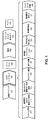
図1は、集積回路の設計および製作における種々のステップを図示する。工程は、製品アイディア100で始まり、その製品アイディア100は、電子設計自動化(EDA)ソフトウェア110を使用することで具現化される。チップ170は、製作150ステップならびにパッケージおよび組み立て160ステップを行うことにより、完結した設計から製造される。
FIG. 1 illustrates various steps in the design and fabrication of an integrated circuit. The process begins with a
EDAソフトウェア110を使用する設計の流れは、以下に説明される。設計の流れの説明は、例証の目的のためだけであって、本発明を制限することは意図されないということを留意されたい。たとえば、実際の集積回路設計は、以下で説明される順序とは異なる順序で設計の流れのステップを行うことを設計者に要求しうる。
The design flow using EDA
システム設計ステップ112において、設計者らは、インプリメントする機能性を記述しうる。設計者らは、機能性を高め、かつコストをチェックするために、起こりうる事態の計画も行いうる。さらに、ハードウェア‐ソフトウェアのアーキテクチャを分割することは、このステップで生じる。論理設計および機能上の検証ステップ114において、ハードウェア記述言語(HDL)設計は、生成され、かつ機能上の正確さについてチェックされうる。
In the
統合および設計ステップ116において、HDLコードは、対象の技術のために最適化されうるネットリストに翻訳されうる。さらに、試験は、完成したチップをチェックするために設計され、かつインプリメントされうる。ネットリスト検証ステップ118において、ネットリストは、タイミング制限との適合性について、およびHDLコードとの対応についてチェックされうる。
In the integration and design step 116, the HDL code may be translated into a netlist that can be optimized for the subject technology. Furthermore, the test can be designed and implemented to check the completed chip. In the
設計計画ステップ120において、チップについての全部のフロアプランが描かれ、かつタイミングおよびトップレベルのルーティングについて分析されうる。次に、物理的インプリメンテーションステップ122において、配置およびルーティングが行われうる。
In the
分析および取り出しステップ124において、回路の機能性は、トランジスタレベルで検証されうる。物理的検証ステップ126において、設計は、機能上、製造上、電気的、またはリソグラフィーの問題のいずれも正すためにチェックされうる。
In the analysis and
解像度を高めるステップ128において、幾何学的な操作は、設計の製造可能性を向上させるためにレイアウトに対して行われうる。最後に、マスクデータ準備ステップ130において、設計は、完成したチップを製造するマスクの製造のためにテープアウト140されうる。 In step 128 of increasing the resolution, geometric operations can be performed on the layout to improve the manufacturability of the design. Finally, in a mask data preparation step 130, the design can be taped out 140 for the production of a mask that produces the finished chip.
ひとたび設計要求違反が回路設計において識別されると、回路のセルは、設計要求違反を修正するために調整されうる。たとえば、セットアップ時間違反を修正するために、経路内の1つ以上のセルは、サイズアップされ、経路を横切る信号により経験される遅延を減らしうる。同様に、ホールド時間違反を修正するために、1つ以上のバッファーは、経路に追加され、経路のピンでホールド時間を増加させうる。 Once a design requirement violation is identified in the circuit design, the cells of the circuit can be adjusted to correct the design requirement violation. For example, to correct setup time violations, one or more cells in the path may be sized up to reduce the delay experienced by signals across the path. Similarly, to correct hold time violations, one or more buffers may be added to the path to increase the hold time at the path pins.
設計要求違反を修正するために回路のセルになされる追加の調整は、ECO(engineering change order)と呼ばれる。ECOはタイミング違反を修正することに制限されないということを留意されたい。ECOは、概して、いずれの種類の違反(たとえば、設計要求チェック違反、騒音違反、漏れ違反など)も修正するために使用されうる。 Additional adjustments made to circuit cells to correct design requirement violations are called ECO (engineering change order). Note that ECO is not limited to correcting timing violations. ECO can generally be used to correct any type of violation (eg, design requirement check violation, noise violation, leak violation, etc.).
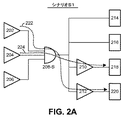
図2Aおよび2Bは、どのように、シナリオにおける設計要求違反を修正することが、別のシナリオにおける別の設計要求違反を生成しうるか、またはさらに悪くしうるかを図示する。 2A and 2B illustrate how modifying a design requirement violation in a scenario can generate or worsen another design requirement violation in another scenario.
ゲート202〜220は、回路設計の一部でありうる。図2Aに図示されるように、回路設計は、シナリオS1において経路222および224に沿ったセットアップタイミング違反を有しうる。シナリオS1のみを考える場合、ゲート208−Sは、タイミング違反を修正するためのECOを適用する良い候補である。特に、ゲート208−Sは、経路222および224に沿ったセットアップタイミング違反を修正するために、より速いゲート(つまり、より小さな遅延値を有するゲート)と取り替えられうる。
The gates 202-220 can be part of the circuit design. As illustrated in FIG. 2A, the circuit design may have setup timing violations along
しかし、図2Bに示されるように、ゲート208−Sをより速いゲートと取り替えることは、シナリオS2において経路226に沿ったホールドタイミング違反を生成しうるか、またはさらに悪くしうる。特に、図2Bは、ゲート208−Sが、ゲート208−Sのより速い型であるゲート208−Fと取り替えられたことを示す。ゲート208−Sがゲート208−Fと取り替えられたとき、シナリオS1において経路222および224に沿ったセットアップ違反を修正したが、シナリオS2において経路226に沿ったホールド違反を生成したか、またはさらに悪くした。
However, as shown in FIG. 2B, replacing gate 208-S with a faster gate may generate or worsen hold timing violations along
これらの理由のため、システム(たとえば、EDAツールを実行するコンピュータシステム)は、設計要求違反を修正するときに複数のシナリオをチェックする必要がある。図2Aおよび2Bにおいて、システムが、設計要求違反を修正するときにシナリオS1とS2との両方をチェックする場合、システムは、ECOを適用する候補としてゲート202、204、および212を選択しうる。たとえば、システムは、ゲート202および204をより速いゲートと取り替え、ゲート212をより遅いゲートと取り替え、それによってシナリオS1において経路222および224に沿ったセットアップタイミング違反を修正し、同時にシナリオS2において経路226に沿ったホールドタイミング違反を修正しうる。同様の考えは、他のタイプの違反が修正されるときにも適用される。
For these reasons, a system (eg, a computer system running an EDA tool) needs to check multiple scenarios when correcting a design requirement violation. In FIGS. 2A and 2B, if the system checks both scenarios S1 and S2 when correcting a design requirement violation, the system may select
図3は複数のシナリオにおける設計要求違反を修正するアプローチを図示する。 FIG. 3 illustrates an approach for correcting design requirement violations in multiple scenarios.
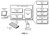
コンピュータシステム302は、プロセッサー304、メモリー306、およびストレージデバイス308を含みうる。コンピュータシステム302は、ディスプレイデバイス314、キーボード310、およびポインティングデバイス312に連結されうる。ストレージデバイス308は、オペレーティングシステム316、アプリケーション318、および異なるシナリオに対応するシナリオイメージ320〜324を記憶しうる。シナリオイメージ320〜324は、特定のシナリオにおいて回路設計の設計要求違反を検出および/または修正するためのアプリケーション318により要求される情報を含みうる。各々のシナリオイメージが概して非常に大きいので、コンピュータシステム302は、所与の時にいつでも、1つのシナリオイメージをメモリー306内に保持することができるだけでありうる。
Computer system 302 can include a processor 304, a
動作中、アプリケーション318は、特定のシナリオに対応するシナリオイメージ(たとえば、シナリオS1に対応するシナリオイメージ320)をストレージ308からメモリー306内へロードしうる。次に、アプリケーション318は、シナリオイメージ320を使用して、シナリオS1における設計要求違反を修正するECOを決定しうる。それから、アプリケーション318は、シナリオイメージ320をメモリー306から除去し、シナリオS2に対応しうるシナリオイメージ322をストレージ308からメモリー306にロードしうる。次に、アプリケーション318は、シナリオイメージ322を使用して、シナリオS1における設計要求違反を修正するように決定されたECOが、新しい設計要求違反を生成するか、またはシナリオS2における現存の設計要求違反をさらに悪くするかどうかをチェックしうる。そのような場合、アプリケーション318は、ECOを却下し、シナリオS1におけるECOの新しいセットを決定することでやり直しうる。一方で、新しい設計要求違反が生成されず、かつ現存の設計要求違反がシナリオS2においてさらに悪くならなかった場合、システムは、次のシナリオに対応する次のシナリオイメージをロードしうる。この態様で、システムは、各々のシナリオにおいてECOをチェックし続けえ、ひとたびECOがすべてのシナリオにおいてチェックされると、システムは、ECOを回路設計に引き渡す。
During operation,
不運にも、ディスク動作の長い呼び出し時間が原因で、シナリオイメージをストレージ308からメモリー306にロードすることは、通例、長い時間がかかる。結果として、上記のアプローチは、複数のシナリオにおける設計要求違反を修正するために実行不可能なほどに長い時間がかかりうる。分散コンピューティングに基づくアプローチは、性能を向上させるために使用されうる。たとえば、各々のシナリオイメージは、分散コンピューティング環境内の別個のコンピュータ内にロードされうる。それから、コンピュータが特定のシナリオのためのECOを決定するとき、コンピュータは、ECOを分散コンピューティング環境内の他のコンピュータに伝達して、異なるシナリオにおいてECOを検証しうる。不運にも、このアプローチは、シナリオの数が多い(たとえば数百)場合、数多くのコンピュータを要求するので、非常に高価でありうる。
Unfortunately, loading scenario images from storage 308 into
本発明のいくつかの実施形態は、複数のシナリオにおける設計要求違反を修正するECOを決定するために要求される時間の量を実質的に減らしうる。いくつかの実施形態は、すべてのシナリオからの情報を含む複数シナリオECOデータベースを生成する。このデータベースは、シナリオイメージと並んでメモリー内に存在しうるほど十分に小さい。システムが、特定のシナリオにおける設計要求違反を修正するECOのセットを決定するとき、システムは、複数シナリオECOデータベースを使用して、すべてのシナリオにわたってECOをチェックしうる。複数シナリオECOデータベースは、システムに、ECOが各々のシナリオにおいて有すると予期される影響を素早く推定することを可能にさせる。 Some embodiments of the present invention may substantially reduce the amount of time required to determine an ECO that corrects a design requirement violation in multiple scenarios. Some embodiments generate a multi-scenario ECO database that includes information from all scenarios. This database is small enough to be in memory alongside the scenario image. When the system determines a set of ECOs that correct design requirement violations in a particular scenario, the system may check the ECO across all scenarios using a multi-scenario ECO database. The multi-scenario ECO database allows the system to quickly estimate the expected impact that the ECO will have in each scenario.
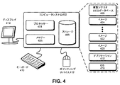
図4は、複数シナリオECOデータベースを使用して、複数のシナリオにおける設計要求違反を修正するアプローチを図示する。 FIG. 4 illustrates an approach for correcting design requirement violations in multiple scenarios using a multiple scenario ECO database.
図3のように、コンピュータシステム402は、プロセッサー404、メモリー406、およびストレージデバイス408を含みうる。コンピュータシステム402は、ディスプレイデバイス414、キーボード410、およびポインティングデバイス412に連結されうる。ストレージデバイス408は、オペレーティングシステム416、アプリケーション418、および異なるシナリオに対応するシナリオイメージ420〜424を記憶しうる。シナリオイメージ420〜424はデータを含みえ、このデータは、特定のシナリオにおいて回路設計の設計要求違反を分析し、シミュレートし、かつ/または修正するためにアプリケーション418により要求される。各々のシナリオイメージが概して非常に大きいので、コンピュータシステム402は、所与の時にいつでも、1つのシナリオイメージをメモリー406内に保持することができるだけでありうる。
As shown in FIG. 3, the computer system 402 can include a
ストレージ408は、複数シナリオECOデータベース426をさらに記憶しうる。複数シナリオECOデータベース426は、複数のシナリオについての回路情報を含みえ、この回路情報は、複数のシナリオにおけるECOの影響を推定するために使用されうる。 Storage 408 can further store a multi-scenario ECO database 426. The multi-scenario ECO database 426 may include circuit information for multiple scenarios, and this circuit information may be used to estimate the impact of ECO in multiple scenarios.
動作中、アプリケーション418は、特定のシナリオに対応するシナリオイメージ(たとえば、シナリオS1に対応するシナリオイメージ420)をストレージ408からメモリー406内にロードしうる。次に、アプリケーション418は、複数シナリオECOデータベース426をメモリー406内にロードしうる。複数シナリオECOデータベース426は、シナリオイメージ420と並んでメモリー406内に存在しうるほど十分に小さくありうる。それから、アプリケーション418は、シナリオイメージ420を使用することで、シナリオS1における設計要求違反を修正するECOを決定し、かつ複数シナリオECOデータベース426を使用することで、ECOが他のシナリオにおいて、新しい設計要求違反を生成することも、現存の設計要求違反をさらに悪くすることも予期されないことを保証しうる。次に、アプリケーション418は、決定されたECOを回路設計に引き渡すか、またはECOが後で回路設計に引き渡されうるように、ECOをストレージ408内に記憶することかのどちらかをしうる。図3におけるアプリケーション318とは違って、アプリケーション418は、他のシナリオにおけるECOの影響をチェックするためにシナリオイメージを交換しないので、アプリケーション418は、他のシナリオにおけるECOの影響をチェックするために要求される時間の量を実質的に減らす。
In operation, application 418 may load a scenario image corresponding to a particular scenario (eg, scenario image 420 corresponding to scenario S1) from storage 408 into
ひとたびシナリオS1に対するECOが、引き渡されるか、またはストレージ408内に記憶されるかのどちらかがされると、アプリケーション418は、別のシナリオに対応する第二のシナリオイメージをロードしうる。たとえば、アプリケーション418は、シナリオS2に対応するシナリオイメージ422をロードしうる。次に、アプリケーション418は、シナリオイメージ422を使用することで、シナリオS2における設計要求違反を修正するECOを決定し、かつ複数シナリオECOデータベース426を使用することで、他のシナリオにおけるECOの影響をチェックしうる。この態様で、システムは、各々のシナリオにおける設計要求違反を修正するECOを決定し、かつ複数シナリオECOデータベースを使用してECOの影響をチェックしうる。 Once the ECO for scenario S1 is either handed over or stored in storage 408, application 418 may load a second scenario image corresponding to another scenario. For example, application 418 may load scenario image 422 corresponding to scenario S2. Next, the application 418 uses the scenario image 422 to determine an ECO that corrects the design requirement violation in the scenario S2, and uses the multi-scenario ECO database 426 to determine the effect of the ECO in other scenarios. Can check. In this manner, the system may determine an ECO that corrects a design requirement violation in each scenario and check the impact of the ECO using a multi-scenario ECO database.
図3および4に示される実施形態は、例証の目的のためだけである。実施形態に対する種々の改変は、当業者にとって容易に明白である。たとえば、一実施形態において、コンピュータシステム402は、コンピュートファームの一部であり、かついずれのユーザーインターフェースデバイスも含まなくてもよく、アプリケーション418は、コンピュートファームに作業として委ねられうる。別の実施形態において、コンピュータ402は、クラウドコンピューティングインフラストラクチャーの一部でありうる。 The embodiments shown in FIGS. 3 and 4 are for illustration purposes only. Various modifications to the embodiments will be readily apparent to those skilled in the art. For example, in one embodiment, the computer system 402 is part of a compute farm and may not include any user interface devices, and the application 418 may be delegated to the compute farm as work. In another embodiment, the computer 402 can be part of a cloud computing infrastructure.
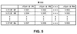
図5は、表形式の複数シナリオECOデータベースの一部を図示する。表500の各々の列はシナリオに対応しえ、各々の行はパラメータ(たとえば、遅延、静電容量、スルーなど)に対応しうる。複数シナリオECOデータベースは、すべてのシナリオにわたって関与する各々の対象(たとえば、ゲート、ネット、ピン、など)についてのパラメータの値を記憶しうる。表500は、回路設計において特定の対象と関連づけられる複数シナリオECOデータベースの一部を表す。たとえば、値V−501〜V−509は、異なるシナリオにおけるゲート208−S(図2Aを参照)と関連づけられるパラメータの値でありうる。 FIG. 5 illustrates a portion of a tabular multi-scenario ECO database. Each column of table 500 may correspond to a scenario, and each row may correspond to a parameter (eg, delay, capacitance, slew, etc.). The multi-scenario ECO database may store parameter values for each subject (eg, gate, net, pin, etc.) involved across all scenarios. Table 500 represents a portion of a multi-scenario ECO database that is associated with a particular object in circuit design. For example, the values V-501 to V-509 can be the values of parameters associated with the gate 208-S (see FIG. 2A) in different scenarios.
複数シナリオECOデータベース内に記憶される情報は、シナリオイメージ(たとえばシナリオイメージ420(図4を参照))内に記憶される情報の小さな断片でありうる。特に、複数シナリオECOデータベースは、異なるシナリオにおけるECOの影響を分析するために要求される対象(たとえば、ゲート、ネット、ピンなど)についての情報を記憶するだけでありうる。たとえば、図2Aおよび2Bにおいて、ゲート214はセットアップタイミング違反経路上にも、ホールドタイミング違反経路上にもないので、ゲート214についての情報は、複数シナリオECOデータベース内に記憶される必要がない。さらに、複数シナリオECOデータベースは、まばらでありえ、つまり、複数シナリオECOデータベースは、異なるシナリオにおけるECOの影響を分析するために要求されるシナリオおよび/またはパラメータだけについての値を記憶しうる。たとえば、図2Aのゲート208−Sが静的漏れ電力バジェットに違反することが予期されない場合、ゲート208−Sの静的漏れ電力についての情報は、複数シナリオECOデータベース内に記憶されなくてもよい。同様に、回路設計が、特定のシナリオにおいていずれの設計要求違反も有さず、またそのシナリオにおいて何か設計要求違反を有することが予期されない場合、複数シナリオECOデータベースは、そのシナリオについてのいずれの情報も記憶しなくてもよい。
The information stored in the multi-scenario ECO database may be a small piece of information stored in a scenario image (eg, scenario image 420 (see FIG. 4)). In particular, the multi-scenario ECO database may only store information about the objects (eg, gates, nets, pins, etc.) required to analyze the effects of ECO in different scenarios. For example, in FIGS. 2A and 2B, information about
表500に示される情報は、特定のゲートと関連づけられうる。システムは、設計要求違反を修正するためにゲートを新しいゲートと取り替えうる。しかし、メモリーおよび複数シナリオECOデータベース内の現用のシナリオイメージは、新しいゲートについてのいずれの情報も有さなくてもよい。したがって、本発明のいくつかの実施形態は、現用のシナリオイメージおよび複数シナリオECOデータベースを使用して、設計要求違反を修正するために使用される取り替えゲートについてのパラメータの値を推定する。 The information shown in table 500 can be associated with a particular gate. The system may replace the gate with a new gate to correct the design requirement violation. However, the current scenario image in the memory and multi-scenario ECO database may not have any information about the new gate. Accordingly, some embodiments of the present invention use the current scenario image and the multi-scenario ECO database to estimate the value of the parameter for the replacement gate that is used to correct the design requirement violation.
たとえば、表500が図2Aに示されるゲート208−Sについてのパラメータの値を記憶すると仮定する。特に、図5におけるパラメータP1がゲート208−Sのゲート遅延に対応すると仮定する。さらに、ゲート208−Sをゲート208−Fと取り替えることが、シナリオS1において、図2Aに示される2つのセットアップ違反を修正することを、システムが決定すると仮定する。その場合、システムは、ゲート208−Sをゲート208−Fと取り替えることが、シナリオS2において何か問題を生成するかどうかをチェックすることを望みうる。しかし、表500は、ゲート208−Fについてのパラメータの値(たとえば、ゲート遅延)を有さず、シナリオS1についてのイメージは、シナリオS2についてのゲート遅延の値を有さない。 For example, assume that table 500 stores values of parameters for gate 208-S shown in FIG. 2A. In particular, assume that parameter P1 in FIG. 5 corresponds to the gate delay of gate 208-S. Further assume that the system determines that replacing gate 208-S with gate 208-F corrects the two setup violations shown in FIG. 2A in scenario S1. In that case, the system may wish to check whether replacing gate 208-S with gate 208-F creates any problems in scenario S2. However, table 500 does not have a parameter value (eg, gate delay) for gate 208-F, and the image for scenario S1 does not have a gate delay value for scenario S2.
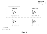
図6は、どのように、パラメータの値が、シナリオイメージおよび複数シナリオECOデータベースを使用して推定されうるかの例を図示する。 FIG. 6 illustrates an example of how parameter values can be estimated using scenario images and a multi-scenario ECO database.
ゲート602についてのパラメータP1の値が、シナリオS1およびS2においてそれぞれ、10および5に等しく、ゲート604についてのパラメータP1の値が、シナリオS1において14に等しいと仮定する。破線の囲みは、複数シナリオECOデータベース内に記憶されうる情報を示し、点線の囲みは、シナリオS1についてのイメージ内に記憶されうる情報を示す。シナリオS2におけるゲート604についてのパラメータP1の値は、シナリオS1についてのイメージ内に記憶されず、複数シナリオECOデータベース内にも記憶されないということを留意されたい。
Assume that the value of parameter P1 for
シナリオS2におけるゲート604についてのパラメータP1の値は、ゲート602をゲート604と取り替えることが、新しい設計要求違反を生成すると予期されるか、またはシナリオS2において現存の設計要求違反をさらに悪くすると予期されるかどうかを決定するために要求されうる。本発明のいくつかの実施形態は、シナリオS1についてのイメージおよび複数シナリオECOデータベース内に含まれる情報に基づいて、シナリオS2におけるゲート604についてのパラメータP1の値を推定する。
The value of parameter P1 for
一般に、システムは、パラメータの値を推定するためにいずれの推定関数も使用しうる。一実施形態において、システムは、シナリオS1およびS2におけるゲート602についてのパラメータP1の値の間の比率を決定し、その比率を使用することにより、シナリオS2におけるゲート604についてのパラメータP1の値を決定しうる。たとえば、図6において、シナリオS1およびS2におけるゲート602についてのパラメータP1の値の間の比率は、2に等しい。それから、この比率は、使用されて、シナリオS2におけるゲート604についてのパラメータP1の値を7であると決定しうる。
In general, the system can use any estimation function to estimate the value of the parameter. In one embodiment, the system determines a ratio between the value of parameter P1 for
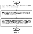
図7は、複数のシナリオにおける設計要求違反を修正する工程を図示するフローチャートを与える。 FIG. 7 provides a flowchart illustrating the process of correcting design requirement violations in multiple scenarios.
工程は、シナリオイメージを受け取ることで始まりえ、そのシナリオイメージは、シナリオにおける回路対象についてのパラメータの値を記憶する(動作702)。 The process may begin by receiving a scenario image that stores the value of a parameter for a circuit object in the scenario (operation 702).
シナリオは、工程コーナー、動作条件、または動作モードのうちの1つ以上と関連づけられうる。シナリオイメージは、詳細なタイミング分析を行うため、および種々の設計要求との適合性をチェックするために使用される情報を含みうる。そのような場合、シナリオイメージは、非常に大きくありえ、コンピュータシステムは、所与の時にいつでも、単一のシナリオイメージをメモリー内に記憶することができるだけでありうる。 A scenario may be associated with one or more of process corners, operating conditions, or operating modes. The scenario image may include information that is used to perform a detailed timing analysis and to check for compliance with various design requirements. In such cases, the scenario image can be very large and the computer system can only store a single scenario image in memory at any given time.
パラメータの値は、回路設計における1つ以上のピンでのタイミングスラックの値、回路設計におけるゲートについての漏れ電力の値、回路設計における1つ以上のピンでの容量性負荷の値および遷移時間の値を含みうるが、これらに制限されない。以下の段落は、設計要求ならびに関連したパラメータの値および回路対象のいくつかの例を説明する。これらの例は、例証の目的のためだけであって、本発明の範囲を制限することは意図されない。 The parameter values include timing slack values at one or more pins in the circuit design, leakage power values for gates in the circuit design, capacitive load values at one or more pins in the circuit design, and transition time values. It can include values, but is not limited to these. The following paragraphs describe some examples of design requirements and associated parameter values and circuit objects. These examples are for illustrative purposes only and are not intended to limit the scope of the invention.
「最大遅延タイミング」要求(別名「セットアップ時間」要求)は、信号にタイミングエンドポイントと関連した必要時間の前にタイミングエンドポイントに到達するように要求する。この設計要求が違反される場合、回路設計は、おそらく、より遅い速度で動作される必要がある。タイミングエンドポイントは、この設計要求を満たす必要がありうる回路対象の例である。タイミングエンドポイントでのスラックの値(たとえば、タイミングエンドポイントでの信号の必要時間と到達時間との間の差)は、ECOがこの設計要求の違反を修正するかどうかを決定するために、シナリオイメージおよび/または複数シナリオECOデータベース内に記憶される必要がありうるパラメータの値の例である。スラックの値の大きさは、タイミングエンドポイントがこの設計要求に違反するときに負であり、タイミングエンドポイントが設計要求を満足するときに正でありうる。 A “maximum delay timing” request (also known as a “setup time” request) requests the signal to reach the timing endpoint before the required time associated with the timing endpoint. If this design requirement is violated, the circuit design probably needs to be run at a slower speed. Timing endpoints are examples of circuit objects that may need to meet this design requirement. The slack value at the timing endpoint (eg, the difference between the required time and arrival time of the signal at the timing endpoint) is used to determine whether the ECO corrects this design requirement violation. FIG. 4 is an example of values of parameters that may need to be stored in an image and / or multi-scenario ECO database. The magnitude of the slack value can be negative when the timing endpoint violates this design requirement and positive when the timing endpoint satisfies the design requirement.
「最小遅延タイミング」要求(別名「ホールド時間」要求)は、信号に必要時間の後にタイミングエンドポイントに到達するように要求する。この設計要求が違反される場合、(たとえば信号がレジスターにより捕捉されなかったので)回路は、おそらく、正常に動作せず、かつ/または不完全な機能性を有する。タイミングエンドポイントは、この設計要求を満たす必要がありうる回路対象の例である。タイミングエンドポイントでのスラックの値(たとえば、タイミングエンドポイントでの信号の必要時間と到達時間との間の差)は、ECOがこの設計要求の違反を修正するかどうかを決定するために、シナリオイメージおよび/または複数シナリオECOデータベース内に記憶される必要がありうるパラメータの値の例である。スラックの値の大きさは、タイミングエンドポイントがこの設計要求に違反するときに負であり、タイミングエンドポイントがこの設計要求を満足するときに正である。 A “minimum delay timing” request (also known as a “hold time” request) requests the signal to reach the timing endpoint after the required time. If this design requirement is violated, the circuit probably does not operate properly and / or has incomplete functionality (eg, because the signal was not captured by the register). Timing endpoints are examples of circuit objects that may need to meet this design requirement. The slack value at the timing endpoint (eg, the difference between the required time and arrival time of the signal at the timing endpoint) is used to determine whether the ECO corrects this design requirement violation. FIG. 4 is an example of values of parameters that may need to be stored in an image and / or multi-scenario ECO database. The magnitude of the slack value is negative when the timing endpoint violates this design requirement and positive when the timing endpoint satisfies this design requirement.
「電気的設計規則」(別名電気的DRC)は、1つ以上の制限を回路対象の1つ以上の電気的性質に課す。電気的設計規則の例は、最大許容信号遷移時間、各々のゲート上の最大許容容量性負荷、ネットの最大許容ファンアウト、およびネットの最大長さを含む。シナリオイメージおよび/または複数シナリオECOデータベース内に記憶される必要がありうるパラメータの値の例は、回路対象の電気的性質の値(たとえば、静電容量)でありうる。この設計規則は、異なるタイプの回路対象に適用されうる。たとえば、最大許容信号遷移時間要求は、タイミングエンドポイントもしくはゲート(たとえば、ゲートの出力での遷移は、ある範囲内になければならない)またはネット(たとえば、ネット上のいずれのピン上の遷移は、ある値より小さくなければならない)に適用されうる。最大許容容量性負荷要求は、論理ゲートに適用されうる。最大許容ファンアウト要求および/または最大長さ要求はネットに適用されうる。 “Electrical Design Rules” (aka Electrical DRC) imposes one or more restrictions on one or more electrical properties of a circuit object. Examples of electrical design rules include the maximum allowable signal transition time, the maximum allowable capacitive load on each gate, the maximum allowable fanout of the net, and the maximum length of the net. An example of a parameter value that may need to be stored in a scenario image and / or a multi-scenario ECO database may be a value of an electrical property of a circuit object (eg, capacitance). This design rule can be applied to different types of circuit objects. For example, the maximum allowable signal transition time requirement is the timing endpoint or gate (eg, the transition at the output of the gate must be within a range) or the net (eg, the transition on any pin on the net is Must be less than a certain value). The maximum allowable capacitive load requirement can be applied to the logic gate. A maximum allowable fanout request and / or a maximum length request may be applied to the net.
「電力バジェット」制約または要求は、1つ以上の制限を回路設計の1つ以上の電力に関連する性質に課しうる。電力に関連する設計要求の例は、回路対象の許容漏れ電力、動的電力、および/または全電力の上限を含む。シナリオイメージおよび/または複数シナリオECOデータベース内に記憶されうるパラメータの値は、回路対象の電力消費の値でありうる。この設計要求は、異なるタイプの回路対象に適用されうる。たとえば、電力に関連する設計要求は、全体の回路設計、または回路設計における各々のリーフレベルのセルインスタンス、または回路設計における特定のブロックに適用されうる。 A “power budget” constraint or requirement may impose one or more limitations on one or more power related properties of the circuit design. Examples of design requirements related to power include circuit object allowable leakage power, dynamic power, and / or an upper limit on total power. The value of the parameter that can be stored in the scenario image and / or the multi-scenario ECO database can be a value of power consumption of the circuit object. This design requirement can be applied to different types of circuit objects. For example, power-related design requirements may apply to the entire circuit design, or each leaf-level cell instance in the circuit design, or a specific block in the circuit design.
図7の論述を続けると、システムは、それから、複数シナリオECOデータベースを受け取りえ、その複数シナリオECOデータベースは、複数のシナリオにおける回路対象の下位セットについてのパラメータの値の下位セットを記憶する(動作704)。複数シナリオECOデータベースは、複数のシナリオにわたって回路対象についての種々のパラメータの値を記憶する。しかし、複数シナリオECOデータベースは、回路対象の下位セットだけについてのパラメータの値の下位セットを記憶する必要があるだけでありうるので、複数シナリオECOデータベースは、シナリオイメージと比べると、サイズが実質的に小さくありうる。 Continuing with the discussion of FIG. 7, the system can then receive a multi-scenario ECO database that stores a sub-set of parameter values for the sub-set of circuit objects in the plurality of scenarios (operations). 704). The multi-scenario ECO database stores various parameter values for circuit objects across multiple scenarios. However, since the multi-scenario ECO database may only need to store a sub-set of parameter values for only the sub-set of the circuit object, the multi-scenario ECO database is substantially smaller in size than the scenario image. Can be small.
いくつかの実施形態において、複数シナリオECOデータベースは、関与する各々のパラメータについての値の範囲を記憶するだけである。範囲は、いずれの所与のシナリオにおいてもパラメータの値がその範囲内にあるように選択される。 In some embodiments, the multi-scenario ECO database only stores a range of values for each parameter involved. The range is chosen so that the value of the parameter is within that range in any given scenario.
いくつかの実施形態において、システムは、既知の設計要求違反に基づいて複数シナリオECOデータベースを築く。たとえば、回路設計が、特定の数の設計要求に違反すると仮定する。システムは、設計要求違反により影響を与えられるパラメータおよび回路対象を決定しうる。次に、システムは、それらのパラメータの値だけを複数シナリオECOデータベース内に記憶しうる。たとえば、図2Aおよび2Bに示されるように、ゲート214は、セットアップタイミング違反経路上にも、ホールドタイミング違反経路上にもないので、ゲート214と関連づけられるパラメータの値は、複数シナリオECOデータベース内に記憶されなくてもよい。
In some embodiments, the system builds a multi-scenario ECO database based on known design requirement violations. For example, assume that a circuit design violates a certain number of design requirements. The system may determine parameters and circuit targets that are affected by design requirement violations. The system may then store only those parameter values in the multi-scenario ECO database. For example, as shown in FIGS. 2A and 2B, since the
いくつかの実施形態において、システムは、既知の設計要求違反および潜在的な設計要求違反に基づいて複数シナリオECOデータベースを築く。たとえば、システムは、違反していないが、違反しそうなパラメータの値を考えうる。たとえば、ゲート214が、タイミング経路上にあり、その経路のスラックがほぼ0である(つまり、ゲート214はタイミング要求に違反しそうである)場合、ゲート214と関連づけられるパラメータの値は、複数シナリオECOデータベース内に記憶されうる。
In some embodiments, the system builds a multi-scenario ECO database based on known design requirement violations and potential design requirement violations. For example, the system may consider parameter values that are not violated but are likely to be violated. For example, if
図7の論述を続けると、システムは、それから、1つ以上の設計要求違反を修正するECOを決定しえ、前記決定することは、シナリオイメージおよび複数シナリオECOデータベース内に記憶されたパラメータの値に基づいて、複数のシナリオにおける回路対象についてのパラメータの値を推定することを含む(動作706)。 Continuing with the discussion of FIG. 7, the system may then determine an ECO that modifies one or more design requirement violations, said determining the value of the parameter stored in the scenario image and the multi-scenario ECO database. And estimating a value of a parameter for a circuit object in a plurality of scenarios (operation 706).
特に、シナリオイメージは、第一のシナリオにおける第一のゲートおよび第二のゲートについてのパラメータの値を記憶しうる。複数シナリオECOデータベースは、第二のシナリオにおける第一のゲートについてのパラメータの値を記憶しうる。システムは、それから、シナリオイメージおよび複数シナリオECOデータベース内に記憶されたパラメータの値に基づいて、第二のシナリオにおける第二のゲートについてのパラメータの値を推定しうる。 In particular, the scenario image may store parameter values for the first gate and the second gate in the first scenario. The multi-scenario ECO database may store parameter values for the first gate in the second scenario. The system may then estimate the value of the parameter for the second gate in the second scenario based on the scenario image and the value of the parameter stored in the multi-scenario ECO database.
(結論)
上記の説明は、当業者の誰もが実施形態を生産し、かつ使用することができるように与えられる。開示された実施形態に対する種々の改変は、当業者にとって容易に明白であり、本明細書中に定義される概括的な原理は、本開示の精神および範囲から逸脱することなく、他の実施形態および用途に応用できる。したがって、本発明は、示される実施形態に制限されずに、本明細書に開示される原理および特徴と一致する最も広い範囲を授けられる。
(Conclusion)
The above description is provided to enable any person skilled in the art to make and use the embodiments. Various modifications to the disclosed embodiments will be readily apparent to those skilled in the art and the generic principles defined herein may be used in other embodiments without departing from the spirit and scope of the disclosure. And can be applied to applications. Accordingly, the invention is not limited to the embodiments shown, but is to be accorded the widest scope consistent with the principles and features disclosed herein.
本開示内に説明されるデータ構造およびコードは、コンピュータ読み取り可能な記憶媒体および/またはハードウェアモジュールおよび/またはハードウェア装置上に部分的にまたは完全に記憶されうる。コンピュータ読み取り可能な記憶媒体は、現時点で既知もしくはのちに開発される、コードおよび/またはデータを記憶することができる揮発性メモリー、不揮発性メモリー、ディスクドライブのような磁気および光学的記憶デバイス、磁気テープ、CD(コンパクトディスク)、DVD(デジタルバーサタイルディスクもしくはデジタルビデオディスク)、または他の媒体を含むが、これらに制限されない。本開示内に説明されるハードウェアモジュールまたは装置は、現時点で既知もしくはのちに開発される特定用途向け集積回路(ASIC)、フィールドプログラマブルゲートアレイ(FPGA)、専用もしくは共有プロセッサー、および/または他のハードウェアモジュールもしくは装置を含むが、これらに制限されない。 The data structures and codes described within this disclosure may be partially or fully stored on computer readable storage media and / or hardware modules and / or hardware devices. Computer-readable storage media include volatile memory, non-volatile memory, magnetic and optical storage devices such as disk drives that are capable of storing code and / or data, known or later developed, magnetic This includes, but is not limited to, tape, CD (compact disc), DVD (digital versatile disc or digital video disc), or other media. The hardware modules or devices described within this disclosure may be any currently known or later developed application specific integrated circuit (ASIC), field programmable gate array (FPGA), dedicated or shared processor, and / or other Including but not limited to hardware modules or devices.
本開示内に説明される方法および工程は、コンピュータ読み取り可能な記憶媒体またはデバイス内に記憶されるコードおよび/またはデータとして部分的にまたは完全に具体化されえ、その結果、コンピュータシステムがコードおよび/またはデータを読み取り、かつ実行するとき、コンピュータシステムは、関連した方法および工程を行う。方法および工程は、ハードウェアモジュールまたは装置内にも部分的にまたは完全に具体化されえ、その結果、ハードウェアモジュールまたは装置が起動されるとき、ハードウェアモジュールまたは装置は関連した方法および工程を行う。方法および工程は、コード、データ、およびハードウェアモジュールもしくは装置の組み合わせを使用することで具体化されうるということを留意されたい。 The methods and steps described within this disclosure may be partially or fully embodied as code and / or data stored in a computer-readable storage medium or device so that the computer system When reading and / or executing data, the computer system performs associated methods and processes. The methods and steps may also be partially or fully embodied in a hardware module or device so that when the hardware module or device is activated, the hardware module or device performs the associated method and step. Do. It should be noted that the methods and steps can be implemented using a combination of code, data, and hardware modules or devices.
本発明の実施形態の上述の説明は、例証および説明の目的のためだけに与えられてきた。上述の説明は、網羅的であることも、本発明を開示された形態に制限することも意図されない。したがって、多数の改変および変化は、当業者にとって明白である。さらに、上記の開示は、本発明を制限することは意図されない。本発明の範囲は、添付の特許請求の範囲により定義される。 The foregoing descriptions of embodiments of the present invention have been given for purposes of illustration and description only. The above description is not intended to be exhaustive or to limit the invention to the form disclosed. Accordingly, many modifications and variations will be apparent to practitioners skilled in this art. Furthermore, the above disclosure is not intended to limit the present invention. The scope of the present invention is defined by the appended claims.
Claims (24)
シナリオイメージを受信することを含み、該シナリオイメージは、シナリオにおける回路対象についてのパラメータの値を記憶しており、
複数シナリオECO(engineering change order)データベースを受信することを含み、該複数シナリオECOデータベースは、前記複数のシナリオにおける回路対象の下位セットについてのパラメータの値の下位セットを記憶しており、
1つ以上のプロセッサによって1つ以上の設計要求違反を修正するECOを決定することとを含み、該決定することは、該シナリオイメージおよび該複数シナリオECOデータベース内に記憶されたパラメータの値に基づいて、前記複数のシナリオの少なくともいくつかにおける回路対象についてのパラメータの値を推定することを含む、
方法。 A method for correcting a design requirement violation of a circuit design in a plurality of scenarios, the method comprising:
Comprises receiving a scenario image, the scenario image, stores the values of parameters for circuit target in the scenario,
Receiving a multi-scenario ECO (engineering change order) database, wherein the multi-scenario ECO database stores a sub-set of parameter values for a sub-set of circuit objects in the plurality of scenarios ,
Determining an ECO that modifies one or more design requirement violations by one or more processors, the determining being based on the scenario image and the values of parameters stored in the multi-scenario ECO database Estimating a value of a parameter for a circuit object in at least some of the plurality of scenarios,
Method.
シナリオイメージを受け取ることであって、該シナリオイメージは、シナリオにおける回路対象についてのパラメータの値を記憶する、ことと、
複数シナリオECO(engineering change order)データベースを受け取ることであって、該複数シナリオECOデータベースは、前記複数のシナリオにおける回路対象の下位セットについてのパラメータの値の下位セットを記憶する、ことと、
1つ以上の設計要求違反を修正するECOを決定することとを含み、該決定することは
、該シナリオイメージおよび該複数シナリオECOデータベース内に記憶されたパラメータの値を使用して、前記複数のシナリオの少なくともいくつかにおける回路対象についてのパラメータの値を推定することを含む、
コンピュータ読み取り可能なプログラム。 A computer readable program, when executed by computer, in the computer, to perform the method of modifying the design requirements violations of the circuit design in a plurality of scenarios, the method comprising,
Receiving a scenario image, wherein the scenario image stores a value of a parameter for a circuit object in the scenario;
Receiving a multi-scenario ECO (engineering change order) database, wherein the multi-scenario ECO database stores a sub-set of parameter values for a sub-set of circuit objects in the plurality of scenarios;
It comprises determining a ECO modifying one or more design requirements violations, to the determination, using the value of the stored parameter in said scenario image and said plurality of scenarios ECO database, the plurality of Estimating the value of a parameter for a circuit object in at least some of the scenarios,
Computer readable program.
プロセッサーと、
メモリーとを含み、該メモリーは、
シナリオイメージであって、該シナリオイメージは、シナリオにおける回路対象についてのパラメータの値を記憶する、シナリオイメージと、
複数シナリオECO(engineering change order)データベースであって、該複数シナリオECOデータベースは、前記複数のシナリオにおける回路対象の下位セットについてのパラメータの値の下位セットを記憶する、複数シナリオECOデータベースと、
命令とを記憶し、該命令は、該プロセッサーにより実行されるとき、該システムに、1つ以上の設計要求違反を修正するECOを決定させ、該決定することは、該シナリオイメージおよび該複数シナリオECOデータベース内に記憶されたパラメータの値を使用して、前記複数のシナリオの少なくともいくつかにおける回路対象についてのパラメータの値を推定することを含む、
システム。 A system comprising:
A processor;
A memory, the memory comprising:
A scenario image, the scenario image storing a parameter value for a circuit object in the scenario; and
A multi-scenario ECO (engineering change order) database, wherein the multi-scenario ECO database stores a sub-set of parameter values for a sub-set of circuit objects in the plurality of scenarios;
Instructions, and when executed by the processor, causes the system to determine an ECO that corrects one or more design requirement violations, and determining the scenario image and the multiple scenarios using the value of the stored parameters in the ECO database comprises estimating the values of parameters for circuit target in at least some of said plurality of scenarios,
system.
前記回路設計における1つ以上のピンでのタイミングスラックの値と、Timing slack values at one or more pins in the circuit design;
前記回路設計における1つ以上のピンでの容量性負荷の値と、A capacitive load value at one or more pins in the circuit design;
前記回路設計における1つ以上のピンでの遷移時間の値と、A transition time value at one or more pins in the circuit design; and
前記回路設計におけるゲートについての漏れ電力の値と、のうちの1つ以上を含む、請求項21に記載のシステム。The system of claim 21, comprising one or more of leakage power values for gates in the circuit design.
セットアップタイミング違反と、Setup timing violation,
ホールドタイミング違反と、Hold timing violation,
電気的設計規則違反と、Violation of electrical design rules,
電力バジェット違反とのうちの1つ以上を含む、請求項21に記載のシステム。The system of claim 21, comprising one or more of power budget violations.
Applications Claiming Priority (3)
| Application Number | Priority Date | Filing Date | Title |
|---|---|---|---|
| US12/949,689 US8407655B2 (en) | 2010-11-18 | 2010-11-18 | Fixing design requirement violations in multiple multi-corner multi-mode scenarios |
| US12/949,689 | 2010-11-18 | ||
| PCT/US2011/061086 WO2012068314A1 (en) | 2010-11-18 | 2011-11-16 | Method and apparatus for fixing design requirement violations in multiple multi-corner multi-mode scenarios |
Publications (2)
| Publication Number | Publication Date |
|---|---|
| JP2014501968A JP2014501968A (en) | 2014-01-23 |
| JP5917543B2 true JP5917543B2 (en) | 2016-05-18 |
Family
ID=46065614
Family Applications (1)
| Application Number | Title | Priority Date | Filing Date |
|---|---|---|---|
| JP2013539990A Active JP5917543B2 (en) | 2010-11-18 | 2011-11-16 | Method and apparatus for correcting design requirement violations in multiple multi-corner multi-mode scenarios |
Country Status (3)
| Country | Link |
|---|---|
| US (1) | US8407655B2 (en) |
| JP (1) | JP5917543B2 (en) |
| WO (1) | WO2012068314A1 (en) |
Families Citing this family (6)
| Publication number | Priority date | Publication date | Assignee | Title |
|---|---|---|---|---|
| US9053264B2 (en) * | 2011-03-16 | 2015-06-09 | Synopsys, Inc. | What-if simulation methods and systems |
| US8875082B1 (en) * | 2012-12-28 | 2014-10-28 | Cadeńce Design Systems, Inc. | System and method for detecting and prescribing physical corrections for timing violations in pruned timing data for electronic circuit design defined by physical implementation data |
| US9026965B2 (en) | 2013-03-12 | 2015-05-05 | Synopsys, Inc. | Arrival edge usage in timing analysis |
| US9280630B1 (en) | 2014-11-07 | 2016-03-08 | International Business Machines Corporation | Modified standard cells to address fast paths |
| US10339258B2 (en) * | 2015-06-30 | 2019-07-02 | Synopsys, Inc. | Look-ahead timing prediction for multi-instance module (MIM) engineering change order (ECO) |
| US10691854B1 (en) * | 2018-11-13 | 2020-06-23 | Avatar Integrated Systems, Inc. | Graph-based timing analysis timing calibration |
Family Cites Families (8)
| Publication number | Priority date | Publication date | Assignee | Title |
|---|---|---|---|---|
| US5018215A (en) * | 1990-03-23 | 1991-05-21 | Honeywell Inc. | Knowledge and model based adaptive signal processor |
| JPH10321725A (en) * | 1997-05-14 | 1998-12-04 | Toshiba Corp | Method and apparatus for designing semiconductor integrated circuit |
| US7315990B2 (en) * | 2004-01-12 | 2008-01-01 | International Business Machines Corporation | Method and system for creating, viewing, editing, and sharing output from a design checking system |
| US7331028B2 (en) * | 2004-07-30 | 2008-02-12 | Lsi Logic Corporation | Engineering change order scenario manager |
| US7454731B2 (en) * | 2006-09-22 | 2008-11-18 | Synopsys, Inc. | Generation of engineering change order (ECO) constraints for use in selecting ECO repair techniques |
| JP5041882B2 (en) * | 2007-06-07 | 2012-10-03 | ルネサスエレクトロニクス株式会社 | Semiconductor integrated circuit design method and design support apparatus |
| JP2009163490A (en) * | 2008-01-07 | 2009-07-23 | Fujitsu Microelectronics Ltd | Integrated circuit timing adjustment method and computer program therefor |
| US20100153897A1 (en) | 2008-12-11 | 2010-06-17 | Lsi Corporation | System and method for employing signoff-quality timing analysis information concurrently in multiple scenarios to reduce leakage power in an electronic circuit and electronic design automation tool incorporating the same |
-
2010
- 2010-11-18 US US12/949,689 patent/US8407655B2/en active Active
-
2011
- 2011-11-16 JP JP2013539990A patent/JP5917543B2/en active Active
- 2011-11-16 WO PCT/US2011/061086 patent/WO2012068314A1/en not_active Ceased
Also Published As
| Publication number | Publication date |
|---|---|
| US8407655B2 (en) | 2013-03-26 |
| WO2012068314A1 (en) | 2012-05-24 |
| US20120131525A1 (en) | 2012-05-24 |
| JP2014501968A (en) | 2014-01-23 |
Similar Documents
| Publication | Publication Date | Title |
|---|---|---|
| KR102324782B1 (en) | Method of performing static timing analysis for an integrated circuit | |
| US8266570B2 (en) | Density-based area recovery in electronic design automation | |
| JP5917543B2 (en) | Method and apparatus for correcting design requirement violations in multiple multi-corner multi-mode scenarios | |
| US8413099B2 (en) | Performing scenario reduction | |
| US10318684B2 (en) | Network flow based framework for clock tree optimization | |
| US8869091B2 (en) | Incremental clock tree synthesis | |
| US9183335B2 (en) | Dynamic power driven clock tree synthesis (CTS) | |
| Han et al. | A global-local optimization framework for simultaneous multi-mode multi-corner clock skew variation reduction | |
| US9141742B2 (en) | Priori corner and mode reduction | |
| US11003821B1 (en) | Deterministic loop breaking in multi-mode multi-corner static timing analysis of integrated circuits | |
| US12073159B2 (en) | Computing device and method for detecting clock domain crossing violation in design of memory device | |
| US9390222B2 (en) | Determining a set of timing paths for creating a circuit abstraction | |
| US9064073B2 (en) | Hyper-concurrent optimization over multi-corner multi-mode scenarios | |
| US10339258B2 (en) | Look-ahead timing prediction for multi-instance module (MIM) engineering change order (ECO) | |
| US9047426B2 (en) | Performing scenario reduction in a circuit design flow | |
| US8418116B2 (en) | Zone-based optimization framework for performing timing and design rule optimization | |
| US20110191731A1 (en) | Zone-based area recovery in electronic design automation | |
| US8707241B2 (en) | Performing scenario reduction using a dominance relation on a set of corners | |
| US8762915B1 (en) | System and method for integrated circuit die size reduction | |
| US10628545B2 (en) | Providing guidance to an equivalence checker when a design contains retimed registers | |
| US10049174B2 (en) | Exact delay synthesis |
Legal Events
| Date | Code | Title | Description |
|---|---|---|---|
| A621 | Written request for application examination |
Free format text: JAPANESE INTERMEDIATE CODE: A621 Effective date: 20140821 |
|
| RD02 | Notification of acceptance of power of attorney |
Free format text: JAPANESE INTERMEDIATE CODE: A7422 Effective date: 20150414 |
|
| RD04 | Notification of resignation of power of attorney |
Free format text: JAPANESE INTERMEDIATE CODE: A7424 Effective date: 20150416 |
|
| A521 | Request for written amendment filed |
Free format text: JAPANESE INTERMEDIATE CODE: A821 Effective date: 20150414 |
|
| A977 | Report on retrieval |
Free format text: JAPANESE INTERMEDIATE CODE: A971007 Effective date: 20150820 |
|
| A131 | Notification of reasons for refusal |
Free format text: JAPANESE INTERMEDIATE CODE: A131 Effective date: 20150929 |
|
| A601 | Written request for extension of time |
Free format text: JAPANESE INTERMEDIATE CODE: A601 Effective date: 20151225 |
|
| A521 | Request for written amendment filed |
Free format text: JAPANESE INTERMEDIATE CODE: A523 Effective date: 20160128 |
|
| TRDD | Decision of grant or rejection written | ||
| A01 | Written decision to grant a patent or to grant a registration (utility model) |
Free format text: JAPANESE INTERMEDIATE CODE: A01 Effective date: 20160322 |
|
| A61 | First payment of annual fees (during grant procedure) |
Free format text: JAPANESE INTERMEDIATE CODE: A61 Effective date: 20160406 |
|
| R150 | Certificate of patent or registration of utility model |
Ref document number: 5917543 Country of ref document: JP Free format text: JAPANESE INTERMEDIATE CODE: R150 |
|
| R250 | Receipt of annual fees |
Free format text: JAPANESE INTERMEDIATE CODE: R250 |
|
| R250 | Receipt of annual fees |
Free format text: JAPANESE INTERMEDIATE CODE: R250 |
|
| R250 | Receipt of annual fees |
Free format text: JAPANESE INTERMEDIATE CODE: R250 |
|
| R250 | Receipt of annual fees |
Free format text: JAPANESE INTERMEDIATE CODE: R250 |
|
| R250 | Receipt of annual fees |
Free format text: JAPANESE INTERMEDIATE CODE: R250 |
|
| R250 | Receipt of annual fees |
Free format text: JAPANESE INTERMEDIATE CODE: R250 |
|
| R250 | Receipt of annual fees |
Free format text: JAPANESE INTERMEDIATE CODE: R250 |