JP5916898B2 - Stacked die assembly with multiple interposers - Google Patents
Stacked die assembly with multiple interposers Download PDFInfo
- Publication number
- JP5916898B2 JP5916898B2 JP2014556545A JP2014556545A JP5916898B2 JP 5916898 B2 JP5916898 B2 JP 5916898B2 JP 2014556545 A JP2014556545 A JP 2014556545A JP 2014556545 A JP2014556545 A JP 2014556545A JP 5916898 B2 JP5916898 B2 JP 5916898B2
- Authority
- JP
- Japan
- Prior art keywords
- interposer
- die
- integrated circuit
- interconnect
- assembly
- Prior art date
- Legal status (The legal status is an assumption and is not a legal conclusion. Google has not performed a legal analysis and makes no representation as to the accuracy of the status listed.)
- Active
Links
- 230000015654 memory Effects 0.000 claims description 84
- 239000000758 substrate Substances 0.000 claims description 43
- 230000006854 communication Effects 0.000 claims description 24
- 238000004891 communication Methods 0.000 claims description 24
- 238000000034 method Methods 0.000 claims description 24
- 230000000712 assembly Effects 0.000 claims description 12
- 238000000429 assembly Methods 0.000 claims description 12
- 229910052751 metal Inorganic materials 0.000 claims description 12
- 239000002184 metal Substances 0.000 claims description 12
- 239000005022 packaging material Substances 0.000 claims description 7
- 230000002457 bidirectional effect Effects 0.000 claims description 5
- 230000004044 response Effects 0.000 claims description 4
- 238000000465 moulding Methods 0.000 claims description 2
- 239000011295 pitch Substances 0.000 description 64
- 229910000679 solder Inorganic materials 0.000 description 56
- 238000010586 diagram Methods 0.000 description 46
- 235000012431 wafers Nutrition 0.000 description 28
- 238000003384 imaging method Methods 0.000 description 18
- 229910052710 silicon Inorganic materials 0.000 description 12
- 239000010703 silicon Substances 0.000 description 12
- XUIMIQQOPSSXEZ-UHFFFAOYSA-N Silicon Chemical compound [Si] XUIMIQQOPSSXEZ-UHFFFAOYSA-N 0.000 description 10
- 241000724291 Tobacco streak virus Species 0.000 description 10
- 230000008878 coupling Effects 0.000 description 8
- 238000010168 coupling process Methods 0.000 description 8
- 238000005859 coupling reaction Methods 0.000 description 8
- 230000007175 bidirectional communication Effects 0.000 description 7
- 238000012545 processing Methods 0.000 description 6
- 239000004020 conductor Substances 0.000 description 5
- 238000001459 lithography Methods 0.000 description 5
- 239000000463 material Substances 0.000 description 5
- PXHVJJICTQNCMI-UHFFFAOYSA-N Nickel Chemical compound [Ni] PXHVJJICTQNCMI-UHFFFAOYSA-N 0.000 description 4
- 230000015572 biosynthetic process Effects 0.000 description 4
- 239000000872 buffer Substances 0.000 description 4
- 230000006870 function Effects 0.000 description 4
- 239000011806 microball Substances 0.000 description 4
- 230000008569 process Effects 0.000 description 4
- 239000004065 semiconductor Substances 0.000 description 4
- 238000005516 engineering process Methods 0.000 description 3
- 238000000608 laser ablation Methods 0.000 description 3
- 238000004806 packaging method and process Methods 0.000 description 3
- RYGMFSIKBFXOCR-UHFFFAOYSA-N Copper Chemical compound [Cu] RYGMFSIKBFXOCR-UHFFFAOYSA-N 0.000 description 2
- VYPSYNLAJGMNEJ-UHFFFAOYSA-N Silicium dioxide Chemical compound O=[Si]=O VYPSYNLAJGMNEJ-UHFFFAOYSA-N 0.000 description 2
- 229910052782 aluminium Inorganic materials 0.000 description 2
- XAGFODPZIPBFFR-UHFFFAOYSA-N aluminium Chemical compound [Al] XAGFODPZIPBFFR-UHFFFAOYSA-N 0.000 description 2
- 239000011805 ball Substances 0.000 description 2
- 230000008901 benefit Effects 0.000 description 2
- 229910052802 copper Inorganic materials 0.000 description 2
- 239000010949 copper Substances 0.000 description 2
- 230000008021 deposition Effects 0.000 description 2
- 238000013461 design Methods 0.000 description 2
- 229910003460 diamond Inorganic materials 0.000 description 2
- 239000010432 diamond Substances 0.000 description 2
- 239000004744 fabric Substances 0.000 description 2
- PCHJSUWPFVWCPO-UHFFFAOYSA-N gold Chemical compound [Au] PCHJSUWPFVWCPO-UHFFFAOYSA-N 0.000 description 2
- 229910052737 gold Inorganic materials 0.000 description 2
- 239000010931 gold Substances 0.000 description 2
- 238000009434 installation Methods 0.000 description 2
- 238000004519 manufacturing process Methods 0.000 description 2
- 229910052759 nickel Inorganic materials 0.000 description 2
- 238000007789 sealing Methods 0.000 description 2
- 238000000926 separation method Methods 0.000 description 2
- 150000003377 silicon compounds Chemical class 0.000 description 2
- 230000003068 static effect Effects 0.000 description 2
- 101100498818 Arabidopsis thaliana DDR4 gene Proteins 0.000 description 1
- 101000822695 Clostridium perfringens (strain 13 / Type A) Small, acid-soluble spore protein C1 Proteins 0.000 description 1
- 101000655262 Clostridium perfringens (strain 13 / Type A) Small, acid-soluble spore protein C2 Proteins 0.000 description 1
- 101000655256 Paraclostridium bifermentans Small, acid-soluble spore protein alpha Proteins 0.000 description 1
- 101000655264 Paraclostridium bifermentans Small, acid-soluble spore protein beta Proteins 0.000 description 1
- 239000000853 adhesive Substances 0.000 description 1
- 230000001070 adhesive effect Effects 0.000 description 1
- 230000003139 buffering effect Effects 0.000 description 1
- 230000032798 delamination Effects 0.000 description 1
- 238000005553 drilling Methods 0.000 description 1
- 238000005530 etching Methods 0.000 description 1
- 239000011521 glass Substances 0.000 description 1
- 239000012535 impurity Substances 0.000 description 1
- 239000011159 matrix material Substances 0.000 description 1
- 239000012778 molding material Substances 0.000 description 1
- 230000003287 optical effect Effects 0.000 description 1
- 238000012856 packing Methods 0.000 description 1
- 150000003071 polychlorinated biphenyls Chemical class 0.000 description 1
- 230000000644 propagated effect Effects 0.000 description 1
- 230000009467 reduction Effects 0.000 description 1
- 235000012239 silicon dioxide Nutrition 0.000 description 1
- 239000000377 silicon dioxide Substances 0.000 description 1
- 238000012546 transfer Methods 0.000 description 1
Images


Classifications
-
- H—ELECTRICITY
- H01—ELECTRIC ELEMENTS
- H01L—SEMICONDUCTOR DEVICES NOT COVERED BY CLASS H10
- H01L25/00—Assemblies consisting of a plurality of individual semiconductor or other solid state devices ; Multistep manufacturing processes thereof
- H01L25/03—Assemblies consisting of a plurality of individual semiconductor or other solid state devices ; Multistep manufacturing processes thereof all the devices being of a type provided for in the same subgroup of groups H01L27/00 - H01L33/00, or in a single subclass of H10K, H10N, e.g. assemblies of rectifier diodes
- H01L25/04—Assemblies consisting of a plurality of individual semiconductor or other solid state devices ; Multistep manufacturing processes thereof all the devices being of a type provided for in the same subgroup of groups H01L27/00 - H01L33/00, or in a single subclass of H10K, H10N, e.g. assemblies of rectifier diodes the devices not having separate containers
- H01L25/065—Assemblies consisting of a plurality of individual semiconductor or other solid state devices ; Multistep manufacturing processes thereof all the devices being of a type provided for in the same subgroup of groups H01L27/00 - H01L33/00, or in a single subclass of H10K, H10N, e.g. assemblies of rectifier diodes the devices not having separate containers the devices being of a type provided for in group H01L27/00
- H01L25/0652—Assemblies consisting of a plurality of individual semiconductor or other solid state devices ; Multistep manufacturing processes thereof all the devices being of a type provided for in the same subgroup of groups H01L27/00 - H01L33/00, or in a single subclass of H10K, H10N, e.g. assemblies of rectifier diodes the devices not having separate containers the devices being of a type provided for in group H01L27/00 the devices being arranged next and on each other, i.e. mixed assemblies
-
- H—ELECTRICITY
- H01—ELECTRIC ELEMENTS
- H01L—SEMICONDUCTOR DEVICES NOT COVERED BY CLASS H10
- H01L23/00—Details of semiconductor or other solid state devices
- H01L23/12—Mountings, e.g. non-detachable insulating substrates
- H01L23/14—Mountings, e.g. non-detachable insulating substrates characterised by the material or its electrical properties
- H01L23/147—Semiconductor insulating substrates
-
- H—ELECTRICITY
- H01—ELECTRIC ELEMENTS
- H01L—SEMICONDUCTOR DEVICES NOT COVERED BY CLASS H10
- H01L23/00—Details of semiconductor or other solid state devices
- H01L23/52—Arrangements for conducting electric current within the device in operation from one component to another, i.e. interconnections, e.g. wires, lead frames
- H01L23/538—Arrangements for conducting electric current within the device in operation from one component to another, i.e. interconnections, e.g. wires, lead frames the interconnection structure between a plurality of semiconductor chips being formed on, or in, insulating substrates
- H01L23/5384—Conductive vias through the substrate with or without pins, e.g. buried coaxial conductors
-
- H—ELECTRICITY
- H01—ELECTRIC ELEMENTS
- H01L—SEMICONDUCTOR DEVICES NOT COVERED BY CLASS H10
- H01L23/00—Details of semiconductor or other solid state devices
- H01L23/52—Arrangements for conducting electric current within the device in operation from one component to another, i.e. interconnections, e.g. wires, lead frames
- H01L23/538—Arrangements for conducting electric current within the device in operation from one component to another, i.e. interconnections, e.g. wires, lead frames the interconnection structure between a plurality of semiconductor chips being formed on, or in, insulating substrates
- H01L23/5385—Assembly of a plurality of insulating substrates
-
- H—ELECTRICITY
- H01—ELECTRIC ELEMENTS
- H01L—SEMICONDUCTOR DEVICES NOT COVERED BY CLASS H10
- H01L25/00—Assemblies consisting of a plurality of individual semiconductor or other solid state devices ; Multistep manufacturing processes thereof
- H01L25/03—Assemblies consisting of a plurality of individual semiconductor or other solid state devices ; Multistep manufacturing processes thereof all the devices being of a type provided for in the same subgroup of groups H01L27/00 - H01L33/00, or in a single subclass of H10K, H10N, e.g. assemblies of rectifier diodes
- H01L25/04—Assemblies consisting of a plurality of individual semiconductor or other solid state devices ; Multistep manufacturing processes thereof all the devices being of a type provided for in the same subgroup of groups H01L27/00 - H01L33/00, or in a single subclass of H10K, H10N, e.g. assemblies of rectifier diodes the devices not having separate containers
- H01L25/065—Assemblies consisting of a plurality of individual semiconductor or other solid state devices ; Multistep manufacturing processes thereof all the devices being of a type provided for in the same subgroup of groups H01L27/00 - H01L33/00, or in a single subclass of H10K, H10N, e.g. assemblies of rectifier diodes the devices not having separate containers the devices being of a type provided for in group H01L27/00
- H01L25/0655—Assemblies consisting of a plurality of individual semiconductor or other solid state devices ; Multistep manufacturing processes thereof all the devices being of a type provided for in the same subgroup of groups H01L27/00 - H01L33/00, or in a single subclass of H10K, H10N, e.g. assemblies of rectifier diodes the devices not having separate containers the devices being of a type provided for in group H01L27/00 the devices being arranged next to each other
-
- H—ELECTRICITY
- H01—ELECTRIC ELEMENTS
- H01L—SEMICONDUCTOR DEVICES NOT COVERED BY CLASS H10
- H01L2224/00—Indexing scheme for arrangements for connecting or disconnecting semiconductor or solid-state bodies and methods related thereto as covered by H01L24/00
- H01L2224/01—Means for bonding being attached to, or being formed on, the surface to be connected, e.g. chip-to-package, die-attach, "first-level" interconnects; Manufacturing methods related thereto
- H01L2224/10—Bump connectors; Manufacturing methods related thereto
- H01L2224/15—Structure, shape, material or disposition of the bump connectors after the connecting process
- H01L2224/16—Structure, shape, material or disposition of the bump connectors after the connecting process of an individual bump connector
- H01L2224/161—Disposition
- H01L2224/16135—Disposition the bump connector connecting between different semiconductor or solid-state bodies, i.e. chip-to-chip
- H01L2224/16145—Disposition the bump connector connecting between different semiconductor or solid-state bodies, i.e. chip-to-chip the bodies being stacked
-
- H—ELECTRICITY
- H01—ELECTRIC ELEMENTS
- H01L—SEMICONDUCTOR DEVICES NOT COVERED BY CLASS H10
- H01L2224/00—Indexing scheme for arrangements for connecting or disconnecting semiconductor or solid-state bodies and methods related thereto as covered by H01L24/00
- H01L2224/01—Means for bonding being attached to, or being formed on, the surface to be connected, e.g. chip-to-package, die-attach, "first-level" interconnects; Manufacturing methods related thereto
- H01L2224/10—Bump connectors; Manufacturing methods related thereto
- H01L2224/15—Structure, shape, material or disposition of the bump connectors after the connecting process
- H01L2224/16—Structure, shape, material or disposition of the bump connectors after the connecting process of an individual bump connector
- H01L2224/161—Disposition
- H01L2224/16151—Disposition the bump connector connecting between a semiconductor or solid-state body and an item not being a semiconductor or solid-state body, e.g. chip-to-substrate, chip-to-passive
- H01L2224/16221—Disposition the bump connector connecting between a semiconductor or solid-state body and an item not being a semiconductor or solid-state body, e.g. chip-to-substrate, chip-to-passive the body and the item being stacked
- H01L2224/16225—Disposition the bump connector connecting between a semiconductor or solid-state body and an item not being a semiconductor or solid-state body, e.g. chip-to-substrate, chip-to-passive the body and the item being stacked the item being non-metallic, e.g. insulating substrate with or without metallisation
- H01L2224/16227—Disposition the bump connector connecting between a semiconductor or solid-state body and an item not being a semiconductor or solid-state body, e.g. chip-to-substrate, chip-to-passive the body and the item being stacked the item being non-metallic, e.g. insulating substrate with or without metallisation the bump connector connecting to a bond pad of the item
-
- H—ELECTRICITY
- H01—ELECTRIC ELEMENTS
- H01L—SEMICONDUCTOR DEVICES NOT COVERED BY CLASS H10
- H01L2224/00—Indexing scheme for arrangements for connecting or disconnecting semiconductor or solid-state bodies and methods related thereto as covered by H01L24/00
- H01L2224/01—Means for bonding being attached to, or being formed on, the surface to be connected, e.g. chip-to-package, die-attach, "first-level" interconnects; Manufacturing methods related thereto
- H01L2224/10—Bump connectors; Manufacturing methods related thereto
- H01L2224/15—Structure, shape, material or disposition of the bump connectors after the connecting process
- H01L2224/16—Structure, shape, material or disposition of the bump connectors after the connecting process of an individual bump connector
- H01L2224/161—Disposition
- H01L2224/16151—Disposition the bump connector connecting between a semiconductor or solid-state body and an item not being a semiconductor or solid-state body, e.g. chip-to-substrate, chip-to-passive
- H01L2224/16221—Disposition the bump connector connecting between a semiconductor or solid-state body and an item not being a semiconductor or solid-state body, e.g. chip-to-substrate, chip-to-passive the body and the item being stacked
- H01L2224/16225—Disposition the bump connector connecting between a semiconductor or solid-state body and an item not being a semiconductor or solid-state body, e.g. chip-to-substrate, chip-to-passive the body and the item being stacked the item being non-metallic, e.g. insulating substrate with or without metallisation
- H01L2224/16235—Disposition the bump connector connecting between a semiconductor or solid-state body and an item not being a semiconductor or solid-state body, e.g. chip-to-substrate, chip-to-passive the body and the item being stacked the item being non-metallic, e.g. insulating substrate with or without metallisation the bump connector connecting to a via metallisation of the item
-
- H—ELECTRICITY
- H01—ELECTRIC ELEMENTS
- H01L—SEMICONDUCTOR DEVICES NOT COVERED BY CLASS H10
- H01L2224/00—Indexing scheme for arrangements for connecting or disconnecting semiconductor or solid-state bodies and methods related thereto as covered by H01L24/00
- H01L2224/01—Means for bonding being attached to, or being formed on, the surface to be connected, e.g. chip-to-package, die-attach, "first-level" interconnects; Manufacturing methods related thereto
- H01L2224/10—Bump connectors; Manufacturing methods related thereto
- H01L2224/15—Structure, shape, material or disposition of the bump connectors after the connecting process
- H01L2224/17—Structure, shape, material or disposition of the bump connectors after the connecting process of a plurality of bump connectors
- H01L2224/171—Disposition
- H01L2224/1718—Disposition being disposed on at least two different sides of the body, e.g. dual array
- H01L2224/17181—On opposite sides of the body
-
- H—ELECTRICITY
- H01—ELECTRIC ELEMENTS
- H01L—SEMICONDUCTOR DEVICES NOT COVERED BY CLASS H10
- H01L25/00—Assemblies consisting of a plurality of individual semiconductor or other solid state devices ; Multistep manufacturing processes thereof
- H01L25/18—Assemblies consisting of a plurality of individual semiconductor or other solid state devices ; Multistep manufacturing processes thereof the devices being of types provided for in two or more different subgroups of the same main group of groups H01L27/00 - H01L33/00, or in a single subclass of H10K, H10N
-
- H—ELECTRICITY
- H01—ELECTRIC ELEMENTS
- H01L—SEMICONDUCTOR DEVICES NOT COVERED BY CLASS H10
- H01L2924/00—Indexing scheme for arrangements or methods for connecting or disconnecting semiconductor or solid-state bodies as covered by H01L24/00
- H01L2924/15—Details of package parts other than the semiconductor or other solid state devices to be connected
- H01L2924/151—Die mounting substrate
- H01L2924/1515—Shape
- H01L2924/15151—Shape the die mounting substrate comprising an aperture, e.g. for underfilling, outgassing, window type wire connections
-
- H—ELECTRICITY
- H01—ELECTRIC ELEMENTS
- H01L—SEMICONDUCTOR DEVICES NOT COVERED BY CLASS H10
- H01L2924/00—Indexing scheme for arrangements or methods for connecting or disconnecting semiconductor or solid-state bodies as covered by H01L24/00
- H01L2924/15—Details of package parts other than the semiconductor or other solid state devices to be connected
- H01L2924/151—Die mounting substrate
- H01L2924/1517—Multilayer substrate
- H01L2924/15192—Resurf arrangement of the internal vias
-
- H—ELECTRICITY
- H01—ELECTRIC ELEMENTS
- H01L—SEMICONDUCTOR DEVICES NOT COVERED BY CLASS H10
- H01L2924/00—Indexing scheme for arrangements or methods for connecting or disconnecting semiconductor or solid-state bodies as covered by H01L24/00
- H01L2924/15—Details of package parts other than the semiconductor or other solid state devices to be connected
- H01L2924/151—Die mounting substrate
- H01L2924/153—Connection portion
- H01L2924/1531—Connection portion the connection portion being formed only on the surface of the substrate opposite to the die mounting surface
- H01L2924/15311—Connection portion the connection portion being formed only on the surface of the substrate opposite to the die mounting surface being a ball array, e.g. BGA
-
- H—ELECTRICITY
- H01—ELECTRIC ELEMENTS
- H01L—SEMICONDUCTOR DEVICES NOT COVERED BY CLASS H10
- H01L2924/00—Indexing scheme for arrangements or methods for connecting or disconnecting semiconductor or solid-state bodies as covered by H01L24/00
- H01L2924/15—Details of package parts other than the semiconductor or other solid state devices to be connected
- H01L2924/151—Die mounting substrate
- H01L2924/156—Material
- H01L2924/157—Material with a principal constituent of the material being a metal or a metalloid, e.g. boron [B], silicon [Si], germanium [Ge], arsenic [As], antimony [Sb], tellurium [Te] and polonium [Po], and alloys thereof
-
- H—ELECTRICITY
- H01—ELECTRIC ELEMENTS
- H01L—SEMICONDUCTOR DEVICES NOT COVERED BY CLASS H10
- H01L2924/00—Indexing scheme for arrangements or methods for connecting or disconnecting semiconductor or solid-state bodies as covered by H01L24/00
- H01L2924/30—Technical effects
- H01L2924/35—Mechanical effects
- H01L2924/351—Thermal stress
- H01L2924/3511—Warping
-
- H—ELECTRICITY
- H01—ELECTRIC ELEMENTS
- H01L—SEMICONDUCTOR DEVICES NOT COVERED BY CLASS H10
- H01L2924/00—Indexing scheme for arrangements or methods for connecting or disconnecting semiconductor or solid-state bodies as covered by H01L24/00
- H01L2924/30—Technical effects
- H01L2924/37—Effects of the manufacturing process
- H01L2924/37001—Yield
Description
発明の分野
この発明は集積回路デバイス(IC)に関する。特に、この発明は、複数のインターポーザを含むICのためのスタックドダイアセンブリに関する。
The present invention relates to integrated circuit devices (ICs). In particular, the present invention relates to a stacked die assembly for an IC that includes a plurality of interposers.
背景
集積回路は、時とともにより「密に」なってきており、つまりより多くのロジック特徴がICにおいて実現されている。より最近では、スタックドシリコンインターコネクトテクノロジ(「SSIT」)により、1つより多い半導体ダイが単一のパッケージに配置されることが可能にされる。SSIT ICは通信帯域幅に対する需要増に対応するために用いられてもよい。しかしながら、SSITを用いるICは1つより多いダイを有するが、そのようなICは、依然としてピン制約のために著しい帯域幅制約を有する。
Background Integrated circuits are becoming more “dense” with time, meaning that more logic features are implemented in ICs. More recently, stacked silicon interconnect technology (“SSIT”) allows more than one semiconductor die to be placed in a single package. SSIT ICs may be used to meet increasing demand for communication bandwidth. However, although ICs using SSIT have more than one die, such ICs still have significant bandwidth constraints due to pin constraints.
したがって、帯域幅制約がより少ないSSIT ICを提供することが望ましい。 Therefore, it is desirable to provide an SSIT IC with less bandwidth constraints.
概要
ICのためのスタックドダイアセンブリは、第1のインターポーザ、第2のインターポーザ、第1の集積回路ダイ、第2の集積回路ダイ、および複数個の構成要素を含む。第1の集積回路ダイは第1のインターポーザおよび第2のインターポーザに相互接続され、第2の集積回路ダイは第2のインターポーザに相互接続される。複数個の構成要素は、第1の集積回路ダイを第1のインターポーザおよび第2のインターポーザに相互接続する。信号は、第1のインターポーザと第2のインターポーザとの間において、第1の集積回路ダイおよび複数個の構成要素を介してルーティングされる。
SUMMARY A stacked die assembly for an IC includes a first interposer, a second interposer, a first integrated circuit die, a second integrated circuit die, and a plurality of components. The first integrated circuit die is interconnected to the first interposer and the second interposer, and the second integrated circuit die is interconnected to the second interposer. The plurality of components interconnects the first integrated circuit die to the first interposer and the second interposer. The signal is routed between the first interposer and the second interposer via the first integrated circuit die and the plurality of components.
いくつかの例示的なアセンブリにおいては、第1の集積回路ダイを第1のインターポーザおよび第2のインターポーザに相互接続する複数個の構成要素は、第1のインターポーザおよび第2のインターポーザのインターコネクト制限領域の外部に位置し、信号は、第1のインターポーザと第2のインターポーザとの間において、第1の集積回路ダイおよび複数個の構成要素を介してルーティングされて、第1のインターポーザおよび第2のインターポーザのインターコネクト制限領域を回避する。 In some exemplary assemblies, the plurality of components interconnecting the first integrated circuit die to the first interposer and the second interposer are interconnect restriction regions of the first interposer and the second interposer. The signal is routed between the first interposer and the second interposer via the first integrated circuit die and the plurality of components to provide a first interposer and a second interposer. Avoid interposer interconnect restriction areas.
アセンブリは、さらに、第1のインターポーザに結合される第3の集積回路ダイを含むことが可能であり、第1の集積回路ダイは、第2の集積回路ダイと第3の集積回路ダイとの間において通信ブリッジを与える。 The assembly can further include a third integrated circuit die coupled to the first interposer, wherein the first integrated circuit die is a second integrated circuit die and a third integrated circuit die. Give a communication bridge between.
第2のインターポーザは複数個の導電線を含むことが可能である。複数個の構成要素は、複数個のダイからダイへのインターコネクトを含むことが可能である。複数個のダイからダイへのインターコネクトの第1の部分は、第1の集積回路ダイを第1のインターポーザに相互接続することが可能である。複数個のダイからダイへのインターコネクトの第2の部分は、第1の集積回路ダイを第2のインターポーザに相互接続することが可能である。複数個のダイからダイへのインターコネクトの第1の部分および第2の部分は、インターコネクト制限領域の対向する両側に配置され得る。複数個のダイからダイへのインターコネクトの第3の部分は、第2の集積回路ダイを第2のインターポーザに相互接続し得る。第2のインターポーザの複数個の導電線の一部は、第1の集積回路ダイを第2の集積回路ダイに相互接続するために、複数個のダイからダイへのインターコネクトの第2の部分、および複数個のダイからダイへのインターコネクトの第3の部分に結合され得る。複数個のダイからダイへのインターコネクトの第2の部分は、インターコネクト制限領域の外部に位置し得、複数個の導電線の一部は、インターコネクト制限領域に関連付けられる第2のインターポーザのオフセット領域の外部に位置し得る。 The second interposer can include a plurality of conductive lines. The plurality of components can include a plurality of die-to-die interconnects. The first portion of the plurality of die-to-die interconnects can interconnect the first integrated circuit die to the first interconnector. A second portion of the plurality of die-to-die interconnects can interconnect the first integrated circuit die to the second interconnector. The first and second portions of the plurality of die-to-die interconnects may be located on opposite sides of the interconnect restriction region. A third portion of the plurality of die-to-die interconnects may interconnect the second integrated circuit die to the second interconnector. A portion of the plurality of conductive lines of the second interposer includes a second portion of the plurality of die-to-die interconnects for interconnecting the first integrated circuit die to the second integrated circuit die; And a plurality of die-to-die interconnect third portions. The second portion of the plurality of die-to-die interconnects may be located outside the interconnect restricted region, and a portion of the plurality of conductive lines may be in an offset region of a second interconnector associated with the interconnect restricted region. Can be located outside.
第1のインターポーザの第1の縁部および第2のインターポーザの第2の縁部は、互いに当接するために実質的に並んで位置決めされ得る。第1のインターポーザは、第1の縁部とともに境界線を共にする第1の境界を有する、インターコネクト制限領域に関連付けられる第1のオフセット領域を含み得る。第2のインターポーザは、第2の縁部とともに境界線を共にする第2の境界を有する、インターコネクト制限領域に関連付けられる第2のオフセット領域を含み得る。 The first edge of the first interposer and the second edge of the second interposer may be positioned substantially side by side to abut one another. The first interposer may include a first offset region associated with the interconnect restricted region having a first boundary that is co-aligned with the first edge. The second interposer may include a second offset region associated with the interconnect restricted region having a second boundary that is co-aligned with the second edge.
インターコネクト制限領域は、微細ピッチインターコネクトを与えるために用いられる金属層およびビアホール層を含み得ない。 The interconnect restriction region may not include metal layers and via hole layers used to provide fine pitch interconnects.
第1のインターポーザは第1のマスクの組を用いて形成され得、第2のインターポーザは第2のマスクの組を用いて形成され得る。第1のマスクの組は、少なくとも部分的に、第2の集積回路ダイが第1の集積回路ダイとは異なるタイプの集積回路向けであることに応じて、第2のマスクの組とは実質的に異なり得る。 The first interposer can be formed using a first set of masks and the second interposer can be formed using a second set of masks. The first mask set is substantially different from the second mask set in response to the second integrated circuit die being for a different type of integrated circuit than the first integrated circuit die. Can be different.
第1のインターポーザの第1の高さは第2のインターポーザの第2の高さと実質的に同じであり得る。第1のインターポーザの第1の幅および第2のインターポーザの第2の幅は、両方とも、同じリソグラフィの最大幅以下であり得る。 The first height of the first interposer can be substantially the same as the second height of the second interposer. The first width of the first interposer and the second width of the second interposer can both be less than or equal to the maximum width of the same lithography.
第2の集積回路ダイは、メモリダイの鉛直スタック、およびメモリダイの鉛直スタックのためのインターフェイスロジックを含むことが可能である。 The second integrated circuit die can include a vertical stack of memory dies and interface logic for the vertical stack of memory dies.
アセンブリを形成するための方法も記載される。この方法は、複数個の構成要素を用いて第1の集積回路ダイを第1のインターポーザおよび第2のインターポーザに相互接続するステップと、複数個の構成要素を用いて第2の集積回路ダイを第2のインターポーザに相互接続するステップと、信号を、第1のインターポーザと第2のインターポーザとの間において、第1の集積回路ダイおよび複数個の構成要素を介してルーティングするステップとを含む。 A method for forming the assembly is also described. The method includes interconnecting a first integrated circuit die to a first interposer and a second interposer using a plurality of components, and a second integrated circuit die using the plurality of components. Interconnecting to a second interposer and routing signals between the first interposer and the second interposer through the first integrated circuit die and the plurality of components.
いくつかの例示的な方法は、さらに、インターコネクト制限領域を与えるために第1のインターポーザおよび第2のインターポーザの各々の一部を取っておくステップを含む。第1の集積回路ダイを第1のインターポーザおよび第2のインターポーザに相互接続する複数個の構成要素は、第1のインターポーザおよび第2のインターポーザのインターコネクト制限領域の外部に位置し得る。第1のインターポーザと第2のインターポーザとの間において信号をルーティングするステップは、第1のインターポーザおよび第2のインターポーザのインターコネクト制限領域を回避するステップを含み得る。 Some exemplary methods further include saving a portion of each of the first and second interposers to provide an interconnect restricted area. A plurality of components interconnecting the first integrated circuit die to the first interposer and the second interposer may be located outside the interconnect restricted area of the first interposer and the second interposer. Routing the signal between the first interposer and the second interposer may include avoiding an interconnect restricted area of the first interposer and the second interposer.
この方法は、さらに、第3の集積回路ダイを第1のインターポーザに相互接続するステップを含み、第1の集積回路ダイは、第2の集積回路ダイと第3の集積回路ダイとの間に通信ブリッジを与える。 The method further includes interconnecting a third integrated circuit die to the first interposer, wherein the first integrated circuit die is between the second integrated circuit die and the third integrated circuit die. Give a communication bridge.
この方法は、さらに、第1のマスクの組を用いて第1のインターポーザを形成するステップと、第2のマスクの組を用いて第2のインターポーザを形成するステップを含む。第1のマスクの組は、少なくとも部分的に、第2の集積回路ダイが第1の集積回路ダイとは異なるタイプの集積回路向けであることに応じて、第2のマスクの組とは実質的に異なり得る。 The method further includes forming a first interposer using the first set of masks and forming a second interposer using the second set of masks. The first mask set is substantially different from the second mask set in response to the second integrated circuit die being for a different type of integrated circuit than the first integrated circuit die. Can be different.
第1のインターポーザの第1の高さは第2のインターポーザの第2の高さと実質的に同じであり得る。第1のインターポーザの第1の幅および第2のインターポーザの第2の幅は、両方とも、同じリソグラフィの最大幅以下であり得る。 The first height of the first interposer can be substantially the same as the second height of the second interposer. The first width of the first interposer and the second width of the second interposer can both be less than or equal to the maximum width of the same lithography.
第2の集積回路ダイはメモリインターフェイスダイを含むことが可能である。この方法は、さらに、メモリインターフェイスダイにメモリダイの鉛直スタックを相互接続するステップを含む。第2の集積回路ダイは、メモリダイの鉛直スタックのためのインターフェイスロジックを含み得る。 The second integrated circuit die can include a memory interface die. The method further includes interconnecting a vertical stack of memory dies to the memory interface die. The second integrated circuit die may include interface logic for a vertical stack of memory dies.
詳細な説明
以下の説明では、この発明のより完全な説明を与えるために、数多くの具体的な詳細を述べる。しかしながら、当業者には、以下に与える具体的な詳細のすべてを伴わずにこの発明を実施してもよいことが明らかであるはずである。他の事例では、例を曖昧にしないために、周知の特徴を詳細には説明していない。例示を容易にするために、同じ参照符号が異なる図において同じ要素を指すために用いられるが、しかしながら、代替的実施例においては、それら要素は異なってもよい。
DETAILED DESCRIPTION In the following description, numerous specific details are set forth in order to provide a more thorough explanation of the present invention. However, it should be apparent to those skilled in the art that the present invention may be practiced without all of the specific details provided below. In other instances, well-known features have not been described in detail in order not to obscure the examples. For ease of illustration, the same reference numerals are used to refer to the same elements in different figures, however, in alternative embodiments they may be different.
いくつかの図で例示的に図示する例を説明する前に、一般的な導入部がさらなる理解のために与えられる。 Before describing the example illustrated by some figures, a general introduction is provided for further understanding.
これまでに、DDR3またはDDR4 DRAMを伴うメモリプール、またはシリアルリンクを伴うメモリは、ピン制限され、それはICの帯域幅を制限した。たとえば、現在、ライン側帯域幅は毎秒約200ギガビット(「Gbps」)であるが、しかしながら、次世代デバイスは約400Gbpsのライン側帯域幅を有するかもしれない。400Gbpsをサポートするために、DDRメモリは、毎秒約1.2テラビット(「Tbps」)のオーダで帯域幅を有してもよい。 To date, memory pools with DDR3 or DDR4 DRAMs, or memories with serial links have been pin limited, which has limited IC bandwidth. For example, currently the line side bandwidth is about 200 gigabits per second (“Gbps”), however, next generation devices may have a line side bandwidth of about 400 Gbps. To support 400 Gbps, DDR memory may have bandwidth on the order of about 1.2 terabits (“Tbps”) per second.
残念ながら、FPGA上には、従来の方策を用いて1.2Tbpsをサポートするように十分なDDRメモリピンはない。限定ではなく例として、シリアルI/Oを伴うDRAMのようなシリアルメモリは、200Gbpsをサポートするために、電力、接地および他の基準ピンに加えて、256本の信号ピンを伴っている64個のトランシーバを用いてもよい。帯域幅上の別の制限は、ライン側およびシステム側並直列変換器直並列変換器(「SERDES」)に対して利用可能なピンの量と関係した。ある側として、システム側帯域幅はライン側帯域幅より著しく大きく、したがって、システム側インターフェイスはさらなるピンからより多く利益を得るであろう。 Unfortunately, there are not enough DDR memory pins on the FPGA to support 1.2 Tbps using conventional strategies. By way of example and not limitation, a serial memory, such as a DRAM with serial I / O, may support 64 Gbps with 256 signal pins in addition to power, ground and other reference pins to support 200 Gbps. The transceiver may be used. Another limitation on bandwidth related to the amount of pins available for the line side and system side parallel to serial converters ("SERDES"). On the one hand, the system side bandwidth is significantly larger than the line side bandwidth, so the system side interface will benefit more from the additional pins.
スタックドシリコンインターコネクトテクノロジ(「SSIT」)では、1つより多い能動的なダイが、能動的インターポーザであろうと、受動的インターポーザであろうと、インターポーザまたはキャリヤダイに結合されてもよい。限定ではなく明確にするため、受動的なインターポーザが用いられることが仮定されるが、他の実施の形態においては能動的なインターポーザが用いられてもよい。しかし、これまでは、SSITをもってさえ、インターポーザ領域は小さすぎて、たとえば400Gbps適用例のために十分な帯域幅を得るための十分なピン数を提供することが可能ではなかった。 In stacked silicon interconnect technology (“SSIT”), more than one active die may be coupled to an interposer or carrier die, whether it is an active interposer or a passive interposer. For clarity, but not limitation, it is assumed that a passive interposer is used, although an active interposer may be used in other embodiments. However, until now, even with SSIT, the interposer area was too small to provide enough pins to get enough bandwidth, for example for 400 Gbps applications.
しかしながら、ここに記載されるようなインターポーザアセンブリを伴うSSITを用いることによって、より多くのピン部位が、リソグラフィ印刷サイズ制限とともにでさえ利用可能である。したがって、大きな半導体ダイでも、たとえば少なくとも1つの他のダイが単一の集積回路パッケージ内にある状態で1ギガバイトを超えるDDR DRAMを含むことが実現可能である。 However, by using SSIT with an interposer assembly as described herein, more pin sites are available even with lithographic print size limitations. Thus, it is feasible to include more than 1 gigabyte of DDR DRAM with a large semiconductor die, for example, with at least one other die in a single integrated circuit package.
以上の一般的な理解を念頭に置いて、スタックドダイアセンブリのさまざまな例を以下に一般的に説明する。上述の実施の形態のうち1つ以上は特定のタイプのICを用いて例示されるため、そのようなICの詳細な説明を以下に与える。しかしながら、他のタイプのICが本明細書中に記載の技術から恩恵を受けることもあることを理解すべきである。 With the above general understanding in mind, various examples of stacked die assemblies are generally described below. Since one or more of the embodiments described above are illustrated using specific types of ICs, a detailed description of such ICs is provided below. However, it should be understood that other types of ICs may benefit from the techniques described herein.
プログラマブルロジックデバイス(PLD)は、特定された論理機能を実行するようにプログラム可能な周知のタイプの集積回路である。PLDの一種であるフィールドプログラマブルゲートアレイ(FPGA)は典型的に、プログラマブルタイルのアレイを含む。これらのプログラマブルタイルは、たとえば、入力/出力ブロック(IOB)、コンフィギュラブルロジックブロック(CLB)、専用ランダムアクセスメモリブロック(BRAM)、乗算器、デジタル信号処理ブロック(DSP)、プロセッサ、クロックマネージャ、遅延ロックループ(DLL)などを含み得る。本明細書中で用いるように、「含む」および「含んでいる」は、限定なしに含むことを意味する。 A programmable logic device (PLD) is a well-known type of integrated circuit that can be programmed to perform specified logic functions. A field programmable gate array (FPGA), a type of PLD, typically includes an array of programmable tiles. These programmable tiles include, for example, an input / output block (IOB), a configurable logic block (CLB), a dedicated random access memory block (BRAM), a multiplier, a digital signal processing block (DSP), a processor, a clock manager, A delay locked loop (DLL) or the like may be included. As used herein, “including” and “including” mean including without limitation.
各々のプログラマブルタイルは典型的に、プログラマブルインターコネクトおよびプログラマブルロジックの両者を含む。プログラマブルインターコネクトは典型的に、プログラマブルインターコネクトポイント(PIP)によって相互接続された異なる長さの多数のインターコネクト配線を含む。プログラマブルロジックは、たとえば、関数生成器、レジスタ、算術論理などを含み得るプログラマブル素子を用いてユーザ設計のロジックを実現する。 Each programmable tile typically includes both programmable interconnect and programmable logic. Programmable interconnects typically include multiple interconnect wires of different lengths interconnected by programmable interconnect points (PIPs). Programmable logic implements user-designed logic using programmable elements that may include, for example, function generators, registers, arithmetic logic, and the like.
プログラマブルインターコネクトおよびプログラマブルロジックは典型的に、内部構成メモリセルにプログラマブル素子がどのように構成されるかを規定するコンフィギュレーションデータのストリームをロードすることによってプログラムされる。コンフィギュレーションデータは外部デバイスによりメモリから(たとえば外部PROMから)読み出されたりFPGAに書き込まれたりし得る。そうして、個別のメモリセルの集合的な状態がFPGAの機能を決める。 Programmable interconnects and programmable logic are typically programmed by loading a stream of configuration data that defines how programmable elements are configured in internal configuration memory cells. Configuration data may be read from memory (eg, from an external PROM) by an external device or written to the FPGA. Thus, the collective state of the individual memory cells determines the function of the FPGA.
別のタイプのPLDはコンプレックスプログラマブルロジックデバイスまたはCPLDである。CPLDは、共に接続されるとともに、インターコネクトスイッチマトリックスによって入力/出力(I/O)リソースに接続された、2つ以上の「機能ブロック」を含む。CPLDの各々の機能ブロックは、プログラマブルロジックアレイ(PLA)およびプログラマブルアレイロジック(PAL)デバイスで用いられるものと同様の2レベルAND/OR構造を含む。CPLDにおいては、コンフィギュレーションデータは典型的に不揮発性メモリ内のチップ上に記憶される。いくつかのCPLDでは、コンフィギュレーションデータは不揮発性メモリ内のチップ上に記憶され、次いで初期コンフィギュレーション(プログラミング)シーケンスの一部として揮発性メモリにダウンロードされる。 Another type of PLD is a complex programmable logic device or CPLD. A CPLD includes two or more “function blocks” connected together and connected to input / output (I / O) resources by an interconnect switch matrix. Each functional block of the CPLD includes a two-level AND / OR structure similar to that used in programmable logic array (PLA) and programmable array logic (PAL) devices. In CPLDs, configuration data is typically stored on a chip in non-volatile memory. In some CPLDs, configuration data is stored on a chip in non-volatile memory and then downloaded to volatile memory as part of an initial configuration (programming) sequence.
これらのプログラマブルロジックデバイス(PLD)のすべてについて、デバイスの機能性は、その目的のためにデバイスに与えられるデータビットによって制御される。データビットは、揮発性メモリ(たとえばFPGAおよびいくつかのCPLDにおけるようなスタティックメモリセル)、不揮発性メモリ(たとえばいくつかのCPLDにおけるようなFLASHメモリ)、またはいずれの他のタイプのメモリセルにも記憶可能である。 For all of these programmable logic devices (PLDs), the functionality of the device is controlled by data bits provided to the device for that purpose. Data bits can be stored in volatile memory (eg static memory cells as in FPGAs and some CPLDs), non-volatile memory (eg FLASH memory as in some CPLDs), or any other type of memory cell It can be memorized.
他のPLDは、デバイス上のさまざまな素子をプログラマブルに相互接続する金属層などの処理層を適用することによってプログラムされる。これらのPLDはマスクプログラマブルデバイスとして公知である。PLDは、たとえば、ヒューズまたはアンチヒューズ技術を用いる他の態様で実現することもできる。「PLD」および「プログラマブルロジックデバイス」という用語はこれらの例示的なデバイスを含むが、これらに限定されるものではなく、部分的にしかプログラマブルでないデバイスも包含する。たとえば、1つのタイプのPLDは、ハードコード化されたトランジスタロジックと、ハードコード化されたトランジスタロジックをプログラマブルに相互接続するプログラマブルスイッチファブリックとの組合せを含む。 Other PLDs are programmed by applying a processing layer such as a metal layer that programmably interconnects the various elements on the device. These PLDs are known as mask programmable devices. The PLD can also be implemented in other manners using, for example, fuse or antifuse technology. The terms “PLD” and “programmable logic device” include, but are not limited to, these exemplary devices, including devices that are only partially programmable. For example, one type of PLD includes a combination of hard-coded transistor logic and a programmable switch fabric that programmably interconnects the hard-coded transistor logic.
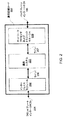
以上注記したように、アドバンストFPGAは、アレイにいくつかの異なるタイプのプログラマブルロジックブロックを含むことができる。たとえば、図1は、マルチギガビットトランシーバ(MGT)101、コンフィギュラブルロジックブロック(CLB)102、ランダムアクセスメモリブロック(BRAM)103、入力/出力ブロック(IOB)104、コンフィギュレーションおよびクロッキングロジック(CONFIG/CLOCKS)105、デジタル信号処理ブロック(DSP)106、専用入力/出力ブロック(I/O)107(たとえばコンフィギュレーションポートおよびクロックポート)、ならびにデジタルクロックマネージャ、アナログ−デジタル変換器、システムモニタロジックなどの他のプログラマブルロジック108を含む多数の異なるプログラマブルタイルを含むFPGAアーキテクチャ100を図示する。いくつかのFPGAは専用プロセッサブロック(PROC)110も含む。
As noted above, advanced FPGAs can include several different types of programmable logic blocks in the array. For example, FIG. 1 shows a multi-gigabit transceiver (MGT) 101, a configurable logic block (CLB) 102, a random access memory block (BRAM) 103, an input / output block (IOB) 104, configuration and clocking logic (CONFIG / CLOCKS) 105, digital signal processing block (DSP) 106, dedicated input / output block (I / O) 107 (eg, configuration port and clock port), and digital clock manager, analog-to-digital converter, system monitor logic, etc. 1 illustrates an
いくつかのFPGAにおいては、各々のプログラマブルタイルは、各々の隣接するタイルにおける対応のインターコネクト素子への、およびそのインターコネクト素子からの、標準化された接続部を有するプログラマブルインターコネクト素子(INT)111を含む。したがって、プログラマブルインターコネクト素子は、図示されるFPGAのためのプログラマブルインターコネクト構造を共に実現する。プログラマブルインターコネクト素子111は、図1の上部に含まれる例によって示されるように、同じタイル内にプログラマブルロジック素子への、およびそのプログラマブルロジック素子からの、接続部も含む。
In some FPGAs, each programmable tile includes a programmable interconnect element (INT) 111 with standardized connections to and from the corresponding interconnect element in each adjacent tile. Thus, the programmable interconnect elements together implement the programmable interconnect structure for the illustrated FPGA.
たとえば、CLB102は、単一のプログラマブルインターコネクト素子(INT)111とともにユーザロジックを実現するようにプログラム可能なコンフィギュラブルロジック素子(CLE)112を含むことができる。BRAM103は、1つ以上のプログラマブルインターコネクト素子に加えてBRAMロジック素子(BRL)113を含むことができる。典型的に、タイルに含まれるインターコネクト素子の数はタイルの高さに依存する。図示される実施の形態では、BRAMタイルは5つのCLBと同じ高さを有するが、他の数(たとえば4つ)を用いることも可能である。DSPタイル106は適切な数のプログラマブルインターコネクト素子に加えてDSPロジック素子(DSPL)114を含むことができる。IOB104は、たとえば、プログラマブルインターコネクト素子111の1つのインスタンスに加えて入力/出力ロジック素子(IOL)115の2つのインスタンスを含むことができる。当業者には明らかなように、たとえばI/Oロジック素子115に接続される実際のI/Oパッドは典型的に、入力/出力ロジック素子115の領域に閉じ込められていない。
For example, the
図示される実施の形態では、(図1に示される)ダイの中央近くの水平方向領域が、コンフィギュレーション、クロックおよび他の制御ロジックのために用いられる。この水平方向領域または列から延在する鉛直方向列109はFPGAの横幅を横切ってクロックおよびコンフィギュレーション信号を分配するのに用いられる。
In the illustrated embodiment, a horizontal area near the center of the die (shown in FIG. 1) is used for configuration, clock and other control logic. This
図1に図示されるアーキテクチャを利用するいくつかのFPGAは、FPGAの大きな部分を形成する規則的な列状構造を分断する付加的なロジックブロックを含む。付加的なロジックブロックはプログラマブルブロックおよび/または専用ロジックであり得る。たとえば、プロセッサブロック110は、CLBおよびBRAMのいくつかの列に跨っている。
Some FPGAs that utilize the architecture illustrated in FIG. 1 include additional logic blocks that break up a regular array of structures that form a large portion of the FPGA. The additional logic block can be a programmable block and / or dedicated logic. For example, the
図1は単に例示的なFPGAアーキテクチャを図示することを意図していることに注目されたい。たとえば、1行の中のロジックブロックの数、行の相対的な幅、行の数および順番、行に含まれるロジックブロックのタイプ、ロジックブロックの相対的なサイズ、ならびに図1の上部に含まれるインターコネクト/ロジック実現例は純粋に例示的なものである。たとえば、実際のFPGAでは、CLBの1つよりも多くの隣接する行は典型的にCLBが現れる場所であればどこでも含まれて、ユーザロジックの効率的な実現を容易にするが、隣接するCLB行の数はFPGAの全体的なサイズとともに変動する。 Note that FIG. 1 is intended only to illustrate an exemplary FPGA architecture. For example, the number of logic blocks in a row, the relative width of the rows, the number and order of the rows, the type of logic block contained in the row, the relative size of the logic blocks, and the top of FIG. The interconnect / logic implementation is purely exemplary. For example, in an actual FPGA, more than one adjacent row of CLBs is typically included wherever a CLB appears, facilitating efficient implementation of user logic, but adjacent CLBs. The number of rows varies with the overall size of the FPGA.
図2は例示的な通信回線カード200を示すブロック図である。通信回線カード200は、1つ以上のインターフェイスモジュール202、通信システム201、ならびにネットワークプロセッサおよびトラフィックマネージャ203を含んでもよい。インターフェイスモジュール202は、フロントプレートインターコネクト204のためにインターコネクトを提供してもよい。フロントプレートインターコネクト204は、インターフェイスモジュール202との双方向通信に対して用いられてもよい。インターフェイスモジュール202の1つ以上は光学的インターコネクトを含んでもよい。
FIG. 2 is a block diagram illustrating an exemplary
インターフェイスモジュール202はライン206を介して通信システム201に結合されてもよい。通信システム201はライン207を介してネットワークプロセッサおよびトラフィックマネージャ203に結合されてもよい。ネットワークプロセッサおよびトラフィックマネージャ203はバックプレーンインターコネクト205に結合されてもよい。ライン206、ライン207およびバックプレーンインターコネクト205は双方向通信に対して用いられてもよいことが理解されるべきである。
図3は例示的な通信システム201を示すブロック図である。通信システム201はたとえば、システム・オン・チップ・ダイ(「SoC」)300および1つ以上のメモリダイ(「メモリプール」)303のような、ICダイを含んでもよい。しかしながら、他の実施の形態では、これらおよび/または他のタイプのICダイの1つ以上が用いられてもよい。SoC300は、たとえばここにおいて先に記載されたように、FPGAとして実現されてもよい。しかしながら、たとえばASIC、ASSPなどのような、他のタイプのICが、SoC300の提供のために用いられてもよいことが理解されるべきである。この例では、SoC300はライン側トランシーバ301と、ライン−システムブリッジ304と、システム側トランシーバ302を含む。ライン206はライン側トランシーバ301に相互接続されてもよく、ライン207はシステム側トランシーバ302に相互接続されてもよい。ライン−システムブリッジ304は、双方向通信のために、システム側トランシーバ302およびライン側トランシーバ301の両方に相互接続されてもよい。
FIG. 3 is a block diagram illustrating an
メモリプール303は双方向通信のためにインターコネクト330を介してライン−システムブリッジ304に相互接続されてもよい。ここに記載されるようなインターポーザの使用によってインターコネクト330に関連付けられるようなより大きなインターコネクト密度を提供することによって、毎秒約1.0テラビット「(Tbps」)以上の帯域幅が与えられてもよい。明確にするため、限定ではなく例として、十分なダブルデータレート(「DDR」)ピンで、400ギガビット以上の回線カードに対するパケットバッファ処理のための帯域幅が、複数の間に置かれたダイ(「インターポーザ」)を用いて最大のレチクル寸法内にフィットしながら提供されてもよい。複数のインターポーザは、少なくとも近接するインターポーザの対、すなわち拡張されたインターポーザを切離せずに、同じウェハ上に印刷することが可能である。別の実施の形態では、インターポーザは、互いから完全に分離され、その後、ブリッジングダイを用いて、互いに結合される。ある実施の形態では、従来のFPGAスライスが、拡張されたインターポーザに対して用いられてもよい。
微細ピッチインターコネクトによって、より下位のレベルの金属層に関連付けられるピッチを伴うインターコネクトが概して意味される。たとえば、いくつかの微細ピッチインターコネクトは0.8ミクロン以下であってもよく、ピッチはワイヤ間隔のためのワイヤ幅を考慮する。他の実施の形態では、いくつかの微細ピッチインターコネクトは0.4ミクロン以下であってもよい。28nmのプロセスにおいて、約90nmまたは0.09ミクロンの密な金属ピッチで微細ピッチインターコネクトを形成することが可能であることが示唆されている。したがって、いくつかの実施の形態では、微細ピッチインターコネクトが100nm未満であるピッチを有してもよいことが理解されるべきである。いくつかの実施の形態では、微細ピッチインターコネクトは、結像フィールドの縁部においてリソグラフィ限界によってサポートされるもの未満、すなわち結像フィールドのフィールド縁部での像の質における低減未満であってもよい。微細ピッチインターコネクトの例は、関連付けられる密なフリップチップマイクロバンプパッドを伴う、密なフリップチップマイクロバンプまたはボールを、限定なしに含む。そのような微細ピッチインターコネクトは、水平および鉛直の最小ピッチが互いとは異なるように、互い違いに配列されたアレイにあってもよい。したがって、微細ピッチインターコネクトは従来のフリップチップマイクロバンプより実質的に密である。 By fine pitch interconnect is generally meant an interconnect with a pitch associated with a lower level metal layer. For example, some fine pitch interconnects may be 0.8 microns or less and the pitch allows for wire width for wire spacing. In other embodiments, some fine pitch interconnects may be 0.4 microns or less. It has been suggested that in a 28 nm process it is possible to form fine pitch interconnects with a dense metal pitch of about 90 nm or 0.09 microns. Thus, it should be understood that in some embodiments, the fine pitch interconnect may have a pitch that is less than 100 nm. In some embodiments, the fine pitch interconnect may be less than that supported by lithographic limits at the edge of the imaging field, i.e. less than a reduction in image quality at the field edge of the imaging field. . Examples of fine pitch interconnects include, without limitation, dense flip chip micro bumps or balls with associated dense flip chip micro bump pads. Such fine pitch interconnects may be in a staggered array such that the horizontal and vertical minimum pitches are different from each other. Thus, the fine pitch interconnect is substantially denser than conventional flip chip micro bumps.
インターポーザアセンブリ310は、ここに記載されるように、単一のICパッケージにおいて、2つ以上のダイがその上またはそれとともに積層される状態で、収容されてもよい。インターポーザアセンブリ310は、同じまたは異なるマスクの組を用いて同じウェハ上に形成された2つ以上のインターポーザを有する拡張されたインターポーザであってもよく、そのような2つ以上のインターポーザは互いから切離されず、すなわちそのようなウェハ上において他の態様ではスクライブ線領域であるかもしれないものにおいて、ともに合わせられたままである。別の実施の形態では、インターポーザアセンブリ310は、さらに詳細に後述されるように、ブリッジングダイによって互いに結合された2つの切離されたダイであってもよい。
明確にするため、限定ではなく例として、メモリプール303は、限定なしにDDR DRAMを含むダブルデータレート(「DDR」)ランダムアクセスメモリ(「RAM」)の形式とともに形成されることが仮定されるが、しかしながら、たとえばQDRのような、他のタイプのメモリインターフェイスを含む他のタイプのメモリが用いられてもよいことが理解されるべきである。
For clarity, by way of example and not limitation, it is assumed that the
一般的に、毎秒400ギガビット(「Gbps」)を超えての通信リンクのためには、パケットバッファ処理ピーク帯域幅は1Tbpsを超える。SSITは、後述されるように、ピン密度が利用可能なインターポーザ領域の最大寸法の増大のために現在利用可能である、十分な数のインターコネクト330がそのようなSoC300とメモリプール303との間に存在するとして、DDRに基づくDRAMを用いて、SoC300とメモリプール303との間において1Tbpsを超えてサポートすることが可能である。
In general, for communication links above 400 gigabits per second (“Gbps”), the packet buffer processing peak bandwidth exceeds 1 Tbps. SSIT has a sufficient number of
図4は別の例示的な通信システム400を示すブロック図である。通信システム400は、図3の通信システム201、インターフェイスモジュール202、ならびにネットワークプロセッサおよびトラフィックマネージャ203を含んでもよい。インターフェイスモジュール202、SoC300およびメモリプール303は、同じインターポーザアセンブリ410に相互接続されてもよい。インターポーザアセンブリ410は、図3のインターポーザアセンブリ310のように、同じまたは異なるマスクの組を用いて同じウェハ上に形成された2つ以上のインターポーザを有する、通信システム400における拡張されたインターポーザであってもよく、そのような2つ以上のインターポーザは互いから切離されず、すなわちそのようなウェハ上において他の態様ではスクライブ線領域であるかもしれないものにおいて、ともに合わせられたままである。別の実施の形態では、インターポーザアセンブリ410は、ブリッジングダイによって互いに結合された別々のインターポーザであってもよい。
FIG. 4 is a block diagram illustrating another
インターフェイスモジュール202、SoC300、メモリプール303、ならびにネットワークプロセッサおよびトラフィックマネージャ203は、同じインターポーザアセンブリ411に相互接続され得、インターポーザアセンブリ411はインターポーザアセンブリ410を含んでもよい。言いかえれば、インターポーザアセンブリ411は、インターポーザアセンブリ410よりもともに合わせられたインターポーザをより多く含んでもよく、したがって、効果的に、インターポーザアセンブリ411はインターポーザアセンブリ410を置換するかまたは含むであろう。1つ以上のFPGAとともに実現されるSoC300に対して、ネットワークプロセッサおよびトラフィックマネージャ203の、1つ以上のネットワークプロセッサおよび/または1つ以上のトラフィックマネージャは、点線412で概ね示されるように、そのような1つ以上のFPGAにおいてインスタンス化されてもよい。
したがって、ここに記載されるようなインターポーザアセンブリを用いて、通信システム400は、インターポーザアセンブリ411を有する、単一のパッケージ化されたIC内に完全に含まれてもよい。通信システム400の別の実施の形態では、インターポーザアセンブリ410を有する、単一のパッケージ化されたICが、プリント回路基板(「PCB」)を介してネットワークプロセッサおよびトラフィックマネージャ203に結合されてもよい。インターポーザが、別々のダイであれ、拡張されたインターポーザであれ、インターポーザに、たとえばSoCまたは他のタイプのICダイのようなICダイでブリッジングすることによって、たとえば微細ピッチインターコネクトのようなダイからダイへのインターコネクトが、たとえばそれぞれ従来のマイクロバンプまたはマイクロボールのような、はるかにより大きな従来のダイからダイへのインターコネクトおよび/またはチップからチップへのインターコネクトに比較して用いられてもよい。したがって、インターコネクト密度は、ダイからダイへの相互接続に対して微細ピッチインターコネクトを伴うインターポーザアセンブリを用いることによって、著しく増強されてもよい。
Thus, using an interposer assembly as described herein, the
図5は例示的な単一のインターポーザ500を示すブロック図である。インターポーザ500は、最大インターポーザ高さ501および最大インターポーザ幅502を有する。これらの最大高さ501および最大幅502は、概してリソグラフィによって決定され、特に、レチクル結像サイズによって限定されてもよい。
FIG. 5 is a block diagram illustrating an exemplary
加えて最大使用可能なインターポーザ領域510を制限するのは、インターポーザ500の縁部からのオフセット511から514である。これらのオフセットは、パッケージ蓋、スクライブ線、封止リング、およびアンダーフィルマージン化、ならびにリソグラフィ結像などのような、パッケージングおよびアセンブリのためのマージンを設けることによってもよい。明確にするため、限定ではなく例として、インターポーザ500は、まずレーザアブレーションを用いてスクライブ線に沿ってトレンチを形成し、次いでダイヤモンドを先端に付けられた円形刃でそのようなレーザ除去されたトレンチに沿って切断することによって、シリコンウェハから切出されてもよい。レーザアブレーションは、ダイヤモンドを先端に付けられた円形刃単独で切断することと比較して、そのような縁部に沿った欠けまたは層間剥離を低減するために用いられてもよい。しかしながら、レーザアブレーションは、ダイヤモンドを先端に付けられた円形刃で切断するよりも広いトレンチを残す傾向がある。
In addition, it is the offsets 511 to 514 from the edge of the
そのようなオフセットを考慮に入れて、最大使用可能なインターポーザ高さ503および最大使用可能なインターポーザ幅504は、最大使用可能なインターポーザ領域510を規定してもよい。しかしながら、この領域のいくらかは、制限された領域であってもよい。さらに詳細に後述されるように、インターポーザアセンブリの左側インターポーザについては、そのような左側インターポーザに対するオフセット領域512のような領域510の一部の右側縁が、「インターコネクト制限領域」の左側縁と整列してもよい。「インターコネクト制限領域」によって、動作する微細ピッチインターコネクトの微細ピッチ整列に対して十分に信頼性がないかまたはそうでなければ利用可能ではない他の領域に関連付けられる領域が概して意味される。たとえば、インターポーザアセンブリの右側インターポーザについては、そのような右側インターポーザの左側縁がそのようなインターコネクト制限領域の右側縁と整列してもよい。右および左が、並んだインターポーザに対して用いられたが、上下の向きが用いられてもよい。
Taking into account such offsets, the maximum
インターコネクト制限領域は、したがって第1のインターポーザおよび第2のインターポーザの、たとえばオフセットのような、部分を含んでもよく、信号は、第1のインターポーザおよび第2のインターポーザのインターコネクト制限領域を回避するために、ブリッジングダイを介してルーティングされる。インターポーザのオフセット領域がレチクル結像フィールドの遠いエッジ領域にあってもよいので、そのような遠いエッジ領域において微細ピッチインターコネクトを結像することは、信頼性高く実行されないかもしれない。対照的に、微細ピッチインターコネクトは、たとえば第1および第2のインターポーザをブリッジングするダイの形成において用いられるような、そのようなレチクル結像フィールドの中心により向かって信頼性高く形成されてもよい。したがって、微細ピッチインターコネクトは、第1および第2のインターポーザのオフセット領域において信頼性高くは整列されないかもしれない一方で、そのような微細ピッチインターコネクトは、そのようなオフセット領域より上においてブリッジングダイにおいて信号を搬送するよう用いられてもよい。 The interconnect restricted area may thus include a portion of the first and second interposers, such as an offset, for example, to avoid the interconnect restricted area of the first and second interposers. Routed through the bridging die. Since the offset region of the interposer may be in the far edge region of the reticle imaging field, imaging the fine pitch interconnect in such a far edge region may not be performed reliably. In contrast, a fine pitch interconnect may be formed more reliably toward the center of such a reticle imaging field, such as used in forming a die that bridges the first and second interposers, for example. . Thus, fine pitch interconnects may not be reliably aligned in the offset regions of the first and second interposers, while such fine pitch interconnects are in bridging dies above such offset regions. It may be used to carry signals.
したがって、概して、微細ピッチインターコネクトは、そのような第1および第2のインターポーザのインターコネクト制限領域の外部で形成され、集積回路ダイを第1のインターポーザおよび第2のインターポーザに相互接続する複数個の構成要素が、インターコネクト制限領域の外部に位置する。対照的に、従来のマイクロバンプは、たとえばインターコネクト制限領域に位置してもよい。インターコネクト制限領域を用いることによって、それに関連付けられる整列問題、たとえば微細ピッチから微細ピッチへの整列などが、限定なしに、ダイ間インターポーザインターコネクトから離れて、重なる近接するレチクル間結像フィールドのシームを含む、レチクル間結像フィールドシームを効果的に位置決めすることによって回避されてもよい。概して、レチクル間結像フィールドシームは、同じレチクルからであれ、異なるレチクルからであれ、リソグラフィ動作の少なくとも2つの結像フィールドが互いと重なる場所である。したがって、たとえば、たとえば1つの能動的なダイ上の1つの群のマイクロバンプから別の能動的なダイ上の別の群のマイクロバンプへのような1つのダイ間インターポーザインターフェイスのための金属ワイヤが、完全に1つのインターポーザレチクルフィールド内において形成されてもよい。特定的には、微細ピッチインターコネクトに関して、そのようなダイ間インターポーザインターフェイスはインターポーザのためのレチクル結像フィールドの遠いエッジ領域から離れるように移動されてもよい。 Thus, in general, a fine pitch interconnect is formed outside the interconnect restricted area of such first and second interposers and includes a plurality of configurations that interconnect the integrated circuit die to the first and second interposers. The element is located outside the interconnect restricted area. In contrast, conventional microbumps may be located, for example, in the interconnect restricted area. By using interconnect limited regions, the alignment problems associated with it, such as fine pitch to fine pitch alignment, include, without limitation, seams of overlapping adjacent inter-reticle imaging fields away from the inter-die interposer interconnect. May be avoided by effectively positioning the inter-reticle imaging field seam. In general, an inter-reticle imaging field seam is where at least two imaging fields of a lithographic operation overlap each other, whether from the same reticle or from different reticles. Thus, for example, metal wires for one die-to-die interposer interface such as from one group of microbumps on one active die to another group of microbumps on another active die. May be formed entirely within one interposer reticle field. In particular, for fine pitch interconnects, such inter-die interposer interface may be moved away from the far edge region of the reticle imaging field for the interposer.
インターコネクト制限領域は、オフセットの領域に関連付けられることに加えて、任意で、増強されたマージンのための右側インターポーザおよび/または左側インターポーザからのような、インターポーザ領域510の、他の態様では使用可能な領域の一部を含んでもよい。ある拡張されたインターポーザにおいては、FPGAダイのようなICダイは、同じウェハからともに合わせられるインターポーザにブリッジングし、たとえばインターポーザアセンブリ310または410のような、インターポーザアセンブリの、右および左のインターポーザからそれぞれオフセット領域511および512にブリッジングする。したがって、そのようなFPGAダイより下のそのようなインターポーザのスクライブ線領域はインターコネクト制限領域の少なくとも一部を形成してもよい。
In addition to being associated with the offset region, the interconnect restricted region can optionally be used in other aspects of the
加えて、拡張されたインターポーザにおいては、ダイシングカットの量が低減されてもよいので、オフセットが同様に低減されてもよく、なぜならば、インターポーザのいくつかの縁部が切断または他の態様で切離されなくてもよいからである。言いかえれば、拡張されたインターポーザのインターポーザアセンブリのインターポーザのダイシングが少なくされ、すなわちいくつかのインターポーザが互いから切離されないので、そのようなインターポーザ間のスクライブ線領域が低減されてもよい。しかしながら、限定ではなく明確にするため、ウェハ上のスクライブ線領域はそのすべてのダイ間でのように概して一様であることが仮定されるが、他の実施の形態ではウェハ上のスクライブ線領域はそのすべてのダイ間におけるように概して一様でなくてもよい。再び、オフセット領域はリソグラフィ結像フィールドの遠いエッジ領域にあってもよく、したがって、そのようなオフセット領域において微細ピッチインターコネクトを信頼性高く形成することは可能ではないかもしれないことが理解されるべきである。 In addition, in an expanded interposer, the amount of dicing cut may be reduced, so the offset may be reduced as well, because some edges of the interposer are cut or otherwise cut. It is because it does not need to be separated. In other words, the interposer dicing of the interposer assembly of the expanded interposer is reduced, i.e., some interposers are not separated from each other, so the scribe line area between such interposers may be reduced. However, for clarity and not limitation, it is assumed that the scribe line area on the wafer is generally uniform, as between all its dies, although in other embodiments the scribe line area on the wafer May not be generally uniform as between all its dies. Again, it should be understood that the offset region may be in the far edge region of the lithographic imaging field, and therefore it may not be possible to reliably form a fine pitch interconnect in such an offset region. It is.
インターコネクト制限領域は、少なくともインターポーザのオフセット領域に応じることに関して記載され、いくつかの実施の形態においては、インターポーザ間の間隙および/またはそうでなければリソグラフィ結像フィールドの幾何学的な限定の対象である1つ以上のインターポーザの使用可能な領域を含んでもよい。インターコネクト制限領域は、あるインターポーザまたは複数のインターポーザの設計に対するデザインルールおよび/またはレイアウトルールとして規定されてもよい。言いかえれば、そのようなインターコネクト制限領域はブリッジングダイが相互接続されたダイ上にあるとして考えられてもよい。そのようなインターポーザの他のインターコネクトと同様に、導電線も、同様にインターコネクト制約に関連付けられてもよい。さらに、インターポーザ間の間隙も、同様にインターコネクト制限領域に関連付けられてもよい。 The interconnect restriction region is described with respect to responding at least to the offset region of the interposer and, in some embodiments, subject to geometric limitations of the gap between the interposers and / or otherwise the lithographic imaging field. One or more interposer usable areas may be included. The interconnect restriction region may be defined as a design rule and / or layout rule for an interposer or multiple interposer designs. In other words, such an interconnect restricted area may be considered as being on the die where the bridging dies are interconnected. As with other interconnects of such an interposer, conductive lines may be associated with interconnect constraints as well. Further, the gap between the interposers may be associated with the interconnect restricted area as well.
概して、限定ではなく明確にするため、インターコネクト制限領域は、ここでは、インターポーザ上において、少なくともそのようなインターポーザのオフセット領域の部分に応じて規定されるように言及される。さらに、限定ではなく明確にするため、インターポーザのインターコネクト制限領域はここではオフセット領域と呼ばれる。さらに、インターコネクト制限領域は、インターポーザが能動素子または受動素子であってもよいので、能動的なダイまたは受動的なダイを含む任意のダイのものであってもよい。しかしながら、限定ではなく明確にするため、インターポーザが受動素子であることが仮定される。さらに、切離されたインターポーザであれ、拡張されたインターポーザであれ、1つのインターポーザを別のインターポーザに接続するブリッジングダイは、能動的なダイまたは受動的なダイであってもよい。それらの線に沿って、ブリッジングダイへの微細ピッチインターコネクトが第1および第2のインターポーザのインターコネクト制限領域の対向する両側に位置してもよいことが十分に理解されるべきである。 In general, for purposes of clarity and not limitation, an interconnect restricted area is referred to herein as being defined on the interposer according to at least a portion of the offset area of such an interposer. Further, for clarity rather than limitation, the interconnect limit area of the interposer is referred to herein as the offset area. Further, the interconnect restricted area may be of any die, including active or passive dies, since the interposer may be an active or passive element. However, for clarity and not limitation, it is assumed that the interposer is a passive element. Further, the bridging die that connects one interposer to another interposer, whether isolated or expanded, may be an active die or a passive die. It should be appreciated that along those lines, fine pitch interconnects to the bridging dies may be located on opposite sides of the interconnect limit areas of the first and second interposers.
限定ではなく、例として明確にするため、最大インターポーザ高さ501はパッケージ蓋設置面積マージン化の後、約31mm(約1.22インチ)であってもよく、現在最大インターポーザ幅502はパッケージ蓋設置面積マージン化の後、約26mm(約1.024インチ)であってもよい。スクライブ線および封止リングオフセットで、最大使用可能なインターポーザ高さ503は約29mm(約1.142インチ)であってもよく、最大使用可能なインターポーザ幅504は約24mm(約0.9449インチ)であってもよい。したがって、現在、最大使用可能なインターポーザ領域510は約700mm2(約27.56平方インチ)であってもよく、この最大使用可能なインターポーザ領域510は、ハイエンドデバイスに対して約600mm2(約23.62平方インチ)以上の現在既存の単一体のダイサイズに鑑み考慮されるべきである。これまで、1ギガビットのメモリはインターポーザ使用可能領域のおおよそ25%〜50%を消費し、したがって、そのような量のメモリは大きなハイエンドデバイスとともにパッケージ化することができなかった。これは、ピン数密度がそのようなインターコネクトのサイズのために著しく制限されることを意味した。しかしながら、1ギガバイトのメモリを用いてバッファ処理することは、効果的には400Gbpsトラフィックの約2.5ミリ秒を占めるにすぎず、それは、トランシーバおよびライン−システムブリッジングの利用に関して不適当な均衡に至るかもしれない。
For purposes of clarity and not limitation, the
以下の記載から十分に理解されるように、より使用可能なインターポーザ領域は、スタックドダイアセンブリを設けるために効果的に2つ以上のインターポーザにブリッジングすることによって設けられる。拡張されたインターポーザについては、これは2つ以上のインターポーザに相互接続される1つ以上のダイを用いることを伴ってもよく、そのようなインターポーザダイは、単一のICパッケージを設けるために単一のプラットフォームとして同じウェハ上に形成される。この例では、2つ以上の分離されたインターポーザが互いと物理的接触をなす実施の形態とは対照的に、2つ以上のインターポーザは、単一のプラットフォームとして互いに物理的に接続される。インターポーザを形成するために用いられるレチクル結像フィールドは、互いと重複してもしなくてもよい。別の実施の形態では、インターポーザは、互いから完全に切離され、次いで、ブリッジングダイを用いて結合されてもよい。さらに別の実施の形態では、インターポーザダイは、たとえば後述されるように、互いから完全に切離され、次いで、単一のICパッケージのためにともに成型され、そしてブリッジングダイでブリッジングされてもよい。 As will be appreciated from the following description, more usable interposer areas are provided by bridging to more than one interposer effectively to provide a stacked die assembly. For extended interposers, this may involve using one or more dies that are interconnected to two or more interposers, and such interposer dies may be used to provide a single IC package. Formed on the same wafer as one platform. In this example, two or more interposers are physically connected to each other as a single platform, as opposed to an embodiment in which two or more separate interposers are in physical contact with each other. The reticle imaging fields used to form the interposer may or may not overlap each other. In another embodiment, the interposers may be completely disconnected from each other and then combined using a bridging die. In yet another embodiment, the interposer dies are completely separated from each other, eg, as described below, and then molded together for a single IC package and bridged with a bridging die. Also good.
図6−1は、たとえばスタックドダイアセンブリ600Aのような、例示的なアセンブリを示すブロック図である。スタックドダイアセンブリ600Aは、SoC300、メモリプール303Aおよび303B、ならびに、拡張されたインターポーザに対してであれ、完全に切離されたインターポーザ500Aおよび500Bに対してであれ、インターポーザ500Aおよび500Bのインターポーザアセンブリを含む。明確にするため、限定ではなく例として、SoC300はFPGAであると仮定するが、しかしながら、他のタイプのICが用いられてもよいことを理解すべきである。
FIG. 6-1 is a block diagram illustrating an exemplary assembly, such as stacked die assembly 600A. Stacked die assembly 600A provides interposer assemblies for
SoC300はライン側トランシーバ301、システム側トランシーバ302A〜302C、およびライン−システムブリッジ304を含んでもよい。ライン側トランシーバ301およびシステム側トランシーバ302A〜302Cはライン−システムブリッジ304を介して双方向通信のために結合されてもよく、そのような結合は、FPGAのPIPを用いることによるようなダイ内結合であってもよい。ライン−システムブリッジ304は、FPGAプログラマブルリソース、すなわち「FPGAファブリック」において実現されてもよい。
The
SoC300は、インターポーザ500Aの表面およびインターポーザ500Bの表面のような、インターポーザ500Aおよび500Bの両方に相互接続されてもよい。たとえば、SoC300は、インターポーザ500Aおよび500Bをブリッジングするようにインターポーザ500Aの上側表面からインターポーザ500Bの上側表面に延在してもよい。拡張されたインターポーザでは、インターポーザ500Aおよび500Bは同じウェハから形成された共通の単一のプラットフォームである。しかしながら、別の実施の形態では、インターポーザ500Aおよび500BはSoC300を介して互いに結合される分離されたインターポーザであってもよい。
点線710Aによって概して示されるように、オフセット領域515の左端の縁部に境を接するインターポーザ500Aの使用可能領域510の一部、および/または点線710Bによって概して示されるように、オフセット領域516の右端の縁部に境を接するインターポーザ500Bの使用可能領域510の一部は、任意で、オフセット領域515および516に応じることに加えて、インターコネクト制限領域599を規定するために用いられるそれぞれの一部であってもよい。しかしながら、限定ではなく明確にするため、さらに詳細に後述されるインターコネクト制限領域599は、オフセット領域515および516に応じてのみ形成されることが仮定されるが、他の実施の形態においては、他の態様で使用可能な領域510の一部が用いられてもよい。
A portion of
SoC300は、従来的に、導電線インターコネクト構成要素を含む、オフセット領域515および516のいずれかまたは両方にある、密なマイクロバンプまたは他の微細ピッチインターコネクトを有してもよいことが理解されるべきである。重ねて、インターポーザのインターコネクト制限領域599はインターコネクトを含んでもよいが、一般的には微細ピッチインターコネクトを含まない。オフセット領域515および516は微細ピッチインターコネクトに対して好適ではないので、SoC300がインターポーザ500Aおよび500Bをブリッジングするのに、それらが互いから切離されていようといまいと、そのようなSoC300の微細ピッチ「ピン配置」レイアウトは従来的でなくてもよい。むしろ、SoC300の微細ピッチ「ピン配置」レイアウトはインターポーザ500Aおよび500Bにブリッジングすることに調整されてもよい。それらの線に沿って、オフセット領域515および516上に配置されるSoC300の微細ピッチインターコネクトは、インターポーザ500Aおよび500Bのオフセット領域515および516内にある、すなわちインターポーザ500Aおよび500Bのインターコネクト制限領域599内にある、粗いピッチインターコネクトに整列されてもよい。
It should be understood that the
メモリプール303Aおよび303Bはインターポーザ500Bの表面に相互接続される。たとえば、メモリプール303Aおよび303Bは、SoC300とのダイ間結合のためにインターポーザ500Bの上側表面に相互接続されてもよい。メモリプール303Aおよび303Bは双方向通信のためにSoC300に結合されてもよい。
インターポーザ500Aおよび500Bは同じまたは実質的に同じ高さを有してもよい。インターポーザ500Aの幅W1は最大インターポーザ幅502以下であってもよく、インターポーザ500Bの幅W2は同様に最大インターポーザ幅502以下であってもよい。しかしながら、幅W1は異なるダイサイズに対応するために幅W2より実質的に大きくてもよい。インターポーザ500Aおよび500Bのインターポーザアセンブリは、幅W1+W2の全体的なインターポーザアセンブリ幅602を有してもよい。限定ではなく、例として明確にするため、インターポーザ500Aおよび500Bの各々に対して約33mm(約1.299インチ)のインターポーザ高さの場合、SoC300が約24ミリメートル(約0.9449インチ)の幅を有する状態で、約40ミリメートル(約1.575インチ)の全体的なインターポーザアセンブリ幅602が用いられてもよい。そのような例に対して、スタックドダイアセンブリ600Aは、単一の50mm(1.969インチ)×50mm(1.969インチ)パッケージ内に嵌まってもよい。しかしながら、他の実施の形態においては、他の高さ、幅、および/またはパッケージサイズが用いられてもよい。
インターポーザ500Aの縁部およびインターポーザ500Bの縁部は、互いに対して少なくとも実質的に並んで位置決めされる。インターポーザ500Aおよび500Bが互いから切離されるとき、インターポーザ500Aおよび500Bのそのような縁部は互いと当接してもよい。インターポーザ500Aは、インターポーザ500Bに概して近い、取っておかれた領域またはオフセット領域515を有してもよい。この例では、オフセット領域515は、インターポーザ500Aの遠い右側縁部と境界線を共にする境界を有する。インターポーザ500Bは、インターポーザ500Aに概して近い、取っておかれた領域またはオフセット領域516を有してもよい。この例では、オフセット領域516は、インターポーザ500Bの遠い左側縁部と境界線を共にする境界を有する。
The edge of
オフセット領域515および516の一方または両方はSoC300の密な微細ピッチピン配置レイアウトにおいて占められてもよく、SoC300は、インターポーザ500Aおよび500Bのそれぞれオフセット領域515および516には関連付けられるが微細ピッチから微細ピッチへのダイからダイへの相互接続には関連付けられない制限領域599内に電気的な相互接続を設けるよう、形成される。オフセット領域515および516のいずれかまたは両方は、それらが動作する微細ピッチから微細ピッチへの電気的な相互接続を設けるよう用いられる金属層部分およびビアホール層部分を含まないように形成されてもよく、したがって、SoC300は、そのようなオフセット領域515および516内において関連付けられる、対応する微細ピッチインターコネクトのためのどのようなピン配置も含まなくてよい。さらに、たとえば、オフセット領域515および516のいずれかまたは両方は、それらが電気的なインターコネクトおよび関連付けられる導電線を含まないように形成されてもよい。
One or both of offset
電気的なインターコネクトは、デバイスの動作のために信号を搬送するために用いられる。電気的なインターコネクトは、たとえばダミー構造体のような、たとえばリソグラフィ結像または他の態様で用いられてもよいような、非電気的な構造のための非電気的なインターコネクトから対比されてもよい。 The electrical interconnect is used to carry signals for device operation. The electrical interconnect may be contrasted with a non-electric interconnect for a non-electric structure, such as a dummy structure, for example, which may be used in lithographic imaging or other manners, for example. .
たとえば後述されるダイからダイへのインターコネクトのような、微細ピッチのダイからダイへのインターコネクトは、SoC300がメモリプール303Aおよび303Bをインターポーザ500Bを介して相互接続することに対して、インターポーザ500B上においてオフセット領域516の外部に排他的に位置してもよい。SoC300をメモリプール303Aおよび303Bに相互接続するための微細ピッチ導電線はすべて、オフセット領域516の外部の、インターポーザ500Bの一部として形成されてもよい。
For example, a fine pitch die-to-die interconnect, such as a die-to-die interconnect described below, is performed on the
接地平面または電源電圧のための幅広いバスを設けることが可能であり、したがって微細ピッチまたは精密な相互接続は、必ずしもそのような幅広いバスに対して必要とはされない。したがって、たとえば、SoC300の1つ以上の微細ピッチインターコネクトは、そのような幅広いバスのためにインターポーザのインターコネクト制限領域に配置されてもよく、なぜならば、微細ピッチ整列制約はそのような幅広いバス化には必ずしも当てはまらないからである。しかしながら、限定ではなく明確にするため、インターコネクト制限領域599はどのような動作するインターコネクトもないことが仮定されるが、他の実施の形態では、微細ピッチ整列制約の対象でないインターコネクトがそのようなインターコネクト制限領域599にあってもよい。
It is possible to provide a wide bus for ground planes or supply voltages, so fine pitch or precise interconnections are not necessarily required for such a wide bus. Thus, for example, one or more fine pitch interconnects of the
図6−2は別の例示的なスタックドダイアセンブリ600Bを示すブロック図である。スタックドダイアセンブリ600Bは、以下の違いを除いて、図6−1のスタックドダイアセンブリ600Aと概ね同じである。単一のSoC300ではなく、スタックドダイアセンブリ600Bは、2つのSoC、すなわちSoC300AおよびSoC300Bを含む。この例では、SoC300Aはライン側トランシーバ301とシステム側トランシーバ302Aとライン−システムブリッジ304Aとを含み、SoC300Bはシステム側トランシーバ302Bおよび302Cとライン−システムブリッジ304Bとを含む。SoC300Aおよび300Bは、インターポーザ500Aに関連付けられるインターコネクトを介して互いに相互接続されてもよい。
FIG. 6-2 is a block diagram illustrating another exemplary stacked die assembly 600B. Stacked die assembly 600B is generally the same as stacked die assembly 600A of FIG. 6-1 except for the following differences. Rather than a
スタックドダイアセンブリ600Aおよび600Bでは、ライン側トランシーバより多いシステム側トランシーバがある。しかしながら、他の構成が用いられてもよい。たとえば、図6−3は、スタックドダイアセンブリのさらに別の例600Cを示すブロック図である。スタックドダイアセンブリ600Cは、以下の違いを除いて、概ね図6−2のスタックドダイアセンブリ600Bと同じである。スタックドダイアセンブリ600Cにおいては、SoC300Aは、ライン側トランシーバ301Aおよびシステム側トランシーバ302Aならびにライン−システムブリッジ304Aを含み、SoC300Bは、ライン側トランシーバ301Bおよびシステム側トランシーバ302Bならびにライン−システムブリッジ304Bを含む。SoC300Aおよび300Bの各々は、インターポーザ500Aおよび500Bを互いに結合することに対して、または互いから切離されないインターポーザ500Aおよび500Bに対して、オフセット領域515および516をブリッジングしてもよい。おおよそ等しい量の半導体領域が、ライン側トランシーバおよびシステム側トランシーバを形成することに対して与えられてもよく、2つのSoCはインターポーザ500Aおよび500Bを物理的にブリッジングするために用いられてもよい。FPGAとともに実現されるSoCについては、トランシーバリソースはライン側またはシステム側のいずれかのために構成されてもよい。
In stacked die assemblies 600A and 600B, there are more system side transceivers than line side transceivers. However, other configurations may be used. For example, FIG. 6-3 is a block diagram illustrating yet another example 600C of a stacked die assembly.
インターポーザ500Aおよび500Bのようなインターポーザは特定のダイに対して製造されてもよいので、インターポーザ500Aを形成するために用いられるマスクの組は、インターポーザ500Bを形成するために用いられるマスクの組とは実質的に異なってもよい。たとえば、あるSoCダイは、限定なしに実質的に異なるサイズおよびピン配置を含んで、メモリダイと実質的に異なってもよい。
Since interposers such as
ここに記載されるようなインターポーザアセンブリを提供することによって、より多くのトランシーバが、概してより多くのリソースと同様に、ライン−システムブリッジングのために、単一のICパッケージにおいてバッファメモリとともに実現されてもよいことが理解されるべきである。さらに、メモリの量は、より大きなインターポーザアセンブリ設置面積を有するため、実質的に増大されてもよい。そのようなリソースは、ICパッケージのためにインターポーザアセンブリにまとめて搭載されてもよいので、ダイからダイへのインターコネクトが、たとえば従来のマイクロバンプより著しく小さく、マイクロボールより実質的に小さい、密なマイクロバンプとともに形成されてもよい。マイクロボールは、時にC4ハンダボールと呼ばれ、従来のマイクロバンプより著しく大きく、従来はPCBを介するICからICへのインターコネクトのために用いられる。 By providing an interposer assembly as described herein, more transceivers are implemented with buffer memory in a single IC package for line-system bridging, generally as well as more resources. It should be understood that it may be. Further, the amount of memory may be substantially increased because it has a larger interposer assembly footprint. Such resources may be mounted together in an interposer assembly for an IC package so that the die-to-die interconnect is denser, for example significantly smaller than conventional microbumps and substantially smaller than microballs. It may be formed together with micro bumps. Microballs, sometimes referred to as C4 solder balls, are significantly larger than conventional microbumps and are conventionally used for IC-to-IC interconnects via PCBs.
言いかえれば、インターコネクト密度は、パッケージ内により大きな設置面積を伴うインターポーザアセンブリを提供することによって増強され、なぜならば、より多くの領域が微細ピッチのダイからダイへの相互接続に対して与えられるからであり、それを、従来のダイからダイへのインターコネクトおよび/またはチップからチップへのインターコネクトの代りに用いてもよい。インターポーザアセンブリを介するインターコネクト密度を増大することによって、帯域幅は、そのようなインターコネクト密度によって対応して増大されてもよい。帯域幅増大は、そのようなさらなるリソースをサポートすることに対して大きなインターポーザアセンブリを有するパッケージ化されたスタックドダイアセンブリ内において利用可能なリソースの追加的な量によってさらに支援されてもよい。 In other words, interconnect density is enhanced by providing an interposer assembly with a larger footprint within the package, because more area is provided for fine pitch die-to-die interconnects. It may be used instead of a conventional die-to-die interconnect and / or a chip-to-chip interconnect. By increasing the interconnect density through the interposer assembly, the bandwidth may be correspondingly increased by such interconnect density. Bandwidth increase may be further aided by an additional amount of resources available in a packaged stacked die assembly having a large interposer assembly for supporting such additional resources.
図7−1は、それぞれ図6−1、図6−2、または図6−3のスタックドダイアセンブリ600A、600Bおよび600Cのいずれか(まとめて1つで「スタックドダイアセンブリ600」)の例示的な断面図を示すブロック図である。SoC300およびメモリプール303は、インターポーザ500Aおよび500Bから形成されるインターポーザアセンブリに、インターコネクト713を介して相互接続される。この例におけるインターコネクト713は密なダイからダイへのフリップチップマイクロバンプであるが、しかしながら、他のタイプのダイからダイへの微細ピッチインターコネクトが用いられてもよい。
FIG. 7-1 is an exemplary illustration of any of the stacked
SoC300は、インターポーザ500Aの上側表面703に、ダイからダイへのインターコネクト713の一部を介して接続されるが、それは微細ピッチインターコネクトであってもよく、または従来のフリップチップマイクロバンプであってもよく、およびSoC300は、インターポーザ500Bの上側表面704に、ダイからダイへのインターコネクト713の別の部分を介して接続される。メモリプール303は、インターポーザ500Bの上側表面704に、ダイからダイへのインターコネクト713のさらに別の部分を介して接続される。ダイからダイへのインターコネクト713のいくつかは、他のより大きなインターコネクトに結合されてもよく、それらは、ここでは、ダイからダイへのインターコネクト(「インターコネクト」)713と混同されないように「コネクタ」711と呼ばれる。たとえば、コネクタ711は、たとえばシリコン貫通ビアホール(「TSV」)712のような、「基板貫通ビアホール」を用いて、インターコネクト713に結合されてもよい。この例では、コネクタ711はマイクロボールであるが、しかしながら、他のタイプのチップからチップへの大規模インターコネクトが用いられてもよい。重ねて、コネクタ711はインターコネクト713より実質的に大きい。したがって、互いに合わせられても、または互いから切離されてもよい、インターポーザ500Aおよび500Bから形成されるインターポーザアセンブリを提供することによって、ダイの相互接続のためのより大きなインターポーザ領域が、チップからチップへのインターコネクトを用いなければならないことを回避するように設けられる。限定ではなく明確にするため、そのようなインターポーザ500Aおよび500Bは、お互いから切離され、すなわち別個のダイであることが仮定される。言いかえれば、ダイからダイへのインターコネクトは、これまではチップからチップへのインターコネクトが用いられたかもしれないところに用いられる。インターコネクト密度は、インターコネクト713での方が、コネクタ711よりも大きいので、帯域幅は先に記載されるようにICのために増強されてもよい。さらに、この例では、インターポーザ500Aおよび500Bはシリコンインターポーザであり、したがって、この例については、基板貫通ビアホールはTSV712であるが、しかしながら、他の実施の形態では、他のタイプの基板またはダイプラットフォームが用いられてもよい。
The
この例におけるインターポーザ500Aの遠い右側縁701は、インターポーザ500Bの遠い左側縁702に当接する。ここにおいて先に記載されたように、縁部701および702はそれぞれオフセット領域515および516の境界を設ける。まとめて、インターポーザ500Aおよび500Bのオフセット領域515および516は、それぞれ、能動的な微細ピッチインターコネクトおよび関連付けられる導電線がなくてもよく、すなわちオフセット領域515および516のすべてまたは部分に対応してもよいインターコネクト制限領域または領域710がなくてもよい。
The far
インターポーザ500Bの上側表面704上のインターコネクト713の一部は、SoC300およびメモリプール303を相互接続するためにある。導電線715のような導電線(以下、1つにまとめて「導電線715」)は、たとえばインターポーザ500Bの層間にあってもよく、SoC300と上側表面704との間に位置するインターコネクト713の一部をメモリプール303と上側表面704との間に位置するインターコネクト713の別の部分と結合するよう用いられる。したがって、SoC300およびメモリプール303の相互接続のための導電線715はすべて、インターポーザ500Bの一部として設けられてもよい。言いかえれば、ダイからダイへの相互接続のための導電線715はすべてインターポーザ500B内で自給自足されてもよい。インターコネクト713および導電線715は、SoC300をメモリプール303に相互接続するために用いられてもよい構成要素の例である。インターコネクト713および導電線715は、1つにまとめて微細ピッチインターコネクトを与えてもよい。
A portion of
図7−2は、別の例示的なスタックドダイアセンブリ700の断面図を示すブロック図である。スタックドダイアセンブリ700は、メモリプール303が、互いに相互接続されたメモリダイの鉛直積層、すなわちスタックドダイメモリ720と置換される以外は、スタックドダイアセンブリ600と同様である。スタックドダイメモリ720はメモリプールダイ(「メモリプール」)303−1〜303−Nを含んでもよく、Nは1より大きな正の整数である。限定ではなく明確にするため図示されないが、メモリプールダイ303−1〜303−Nは、たとえばTSVの使用を介してのように、互いに相互接続されて、スタックドダイメモリ720を与えてもよいことが理解されるべきである。メモリプールダイ303−1は、先にたとえばメモリプール303を参照して記載されたようにインターポーザ500Bに相互接続されてもよい。
FIG. 7-2 is a block diagram illustrating a cross-sectional view of another exemplary stacked
図7−3は、さらに別のスタックドダイアセンブリ700の断面図を示すブロック図である。この例において、メモリプールダイ303−1〜303−Nは、スタックドダイメモリ730の形成のためにメモリインターフェイス731の上に積層される。スタックドダイメモリ730はスタックドダイメモリ720を置換する。メモリインターフェイス731はインターポーザ500Bに相互接続される。メモリインターフェイス731は、メモリプールダイ303−1〜303−Nに対するインターフェイスロジックを含んでもよい。メモリインターフェイス731はメモリプールダイ303−1に相互接続され、スタックドダイメモリ730の構成に依存するその1つ以上の介在するメモリプールダイを介してメモリプールダイ303−1〜303−Nの各々に相互接続されてもよい。
FIG. 7-3 is a block diagram illustrating a cross-sectional view of yet another stacked
図8は、インターポーザアセンブリ800の例示的な上面図を示すブロック図である。インターポーザアセンブリ800はインターポーザ500Aおよび500Bを含む。インターポーザ500Aおよび500Bの各々は、最大インターポーザ高さ501以下であってもよい高さを有する。明確にするため、限定ではなく例として、この例におけるインターポーザ500Aおよび500Bは、両方とも、同じ最大インターポーザ高さ501を有し、同様に、同じ最大使用可能な高さ503を有する。しかしながら、他の実施の形態では、インターポーザ500Aおよび500Bは、少なくとも1つは最大高さにおいてではない不等な高さを有してもよい。
FIG. 8 is a block diagram illustrating an exemplary top view of
インターポーザ500Aおよび500Bの各々は、最大インターポーザ幅502以下であってもよい幅を有する。明確にするため、限定ではなく例として、この例におけるインターポーザ500Aおよび500Bは、両方とも、同じ最大インターポーザ幅502を有し、同様に、同じ最大使用可能な幅504を有する。しかしながら、他の実施の形態では、インターポーザ500Aおよび500Bは、少なくとも1つは最大幅においてではない不等な幅を有してもよい。
Each of
この例では、電気的なインターコネクト制限領域710はインターポーザ500Aおよび500Bのダイにされた縁部と当接することに応じては規定されず、なぜならば、インターポーザ500Aおよび500Bは、この例では、全体として同じウェハまたは他の基板上に形成され、すなわち、単一のプラットフォームとして互いと一体に形成されるからである。言いかえれば、インターポーザ500Aおよび500Bは、2つの別々のプラットフォームとは対照的に、単一のプラットフォームとして形成される。したがって、インターポーザ500Aおよび500Bはこの例では同じ半導体基板から単一のプラットフォームを与える。インターポーザ500Aおよび500Bのオフセット領域515および516を用いて、電気的なインターコネクト制限領域710を規定してもよい。しかしながら、インターポーザ500Aおよび500Bが単一のプラットフォームとして形成されるとき、電気的なインターコネクト制限領域710はスクライブ線シームを含む必要はなく、パッケージングのためにダイにするためにマージン化することを含む必要はない。したがってインターポーザ500Aおよび500Bの拡張されたまたは単一のプラットフォーム版においては、最大使用可能領域は、インターポーザ500Aおよび500Bをダイにし、それから別々のダイを与える実施の形態を超えて増大されてもよく、したがって、インターポーザレチクルフィールドリソグラフィ結像制限の対象であるインターコネクト制限領域710の設置面積は低減されてもよい。
In this example, the electrical
別々のレチクルの組がインターポーザ500Aおよび500Bの形成において用いられるので、そのようなレチクルの組をそのシームを横切ってインターコネクトを形成するために互いと整列させることは問題かもしれない。インターコネクト制限領域710は、整列問題を緩和するために拡大されてもよい。シリコンウェハの例がインターポーザ500Aおよび500Bの形成の記載に対してここに用いられるが、他のタイプの基板が、ガラスまたは別の形式の基板基材を限定なしに含んで、用いられてもよい。
Since separate reticle sets are used in forming the
図9−1は例示的なウェハ900を示すブロック図である。ウェハ900はインターポーザ500Aおよび500Bからインターポーザアセンブリ800を形成するために用いられてもよい。2つの別々のレチクルの組が、インターポーザ500Aおよび500Bの形成のために、ワイヤおよびビアホールを限定なしに含むインターポーザパターンを印刷するよう用いられてもよい。ウェハ900は、水平行901および垂直列902に沿ってレーザ除去および/または鋸引きされてもよい。水平行901および垂直列902はスクライブ線であってもよい。ウェハ900をダイにした後、インターポーザアセンブリ800は、インターポーザ500Aおよび500Bが、同じウェハ基板材料から互いに一体に形成され、単一のプラットフォームのダイとして与えられることが十分に理解されるべきである。
FIG. 9-1 is a block diagram illustrating an
2つのインターポーザがインターポーザアセンブリ800の形成のために例示的に示されるが、2つを超えるインターポーザがダイとして与えられるよう同じウェハ基板材料から互いに一体的に形成されてもよい。たとえば、図9−2は、インターポーザアセンブリ800が各々4つのインターポーザから形成される例示的なウェハ900を示すブロック図である。この例では、インターポーザアセンブリ800は各々インターポーザ500A、500B、500Cおよび500Dを含み、インターポーザのそのような集合は、互いと一体に、単一または共通プラットフォームとして形成される。
Although two interposers are illustratively shown for the formation of
図10−1は、例示的なスタックドダイアセンブリ1000の断面図を示すブロック図である。スタックドダイアセンブリ1000は、当接する縁部701および702ではなく、そのような縁部間の間隙1010が与えられる以外は、スタックドダイアセンブリ600と同様である。縁部701および702は、そのような並んだ向きについて、少なくとも互いに実質的に平行に位置決めされてもされなくてもよい。この例では、間隙1010は制限されたインターコネクト領域1049を効果的に拡張し、したがって、他の態様では間隙1010より上で延在するSoC300下のピン配置であるかもしれないものとして省略されてもよい。SoC300のピン配置を低減するのではなく、SoC300以外のダイを用いて、インターポーザ500Aおよび500Bをブリッジングしてもよい。
FIG. 10-1 is a block diagram illustrating a cross-sectional view of an exemplary
しかしながら、インターポーザ500Aおよび500Bがそれらの間に間隙1010を有する場合、そのようなインターポーザを形成するように用いられるレチクルフィールドに関連付けられるシームは、そのようなインターポーザが異なるウェハから形成される場合には存在しなくてもよいことが理解されるべきである。しかしながら、そのようなオフセット領域515および516は残存し、したがって、限定ではなく明確にするため、インターコネクト制限領域または領域1049は残存し、間隙1010を含む、と仮定される。
However, if the
図10−2は、例示的なスタックドダイアセンブリ1100の断面図を示すブロック図である。スタックドダイアセンブリ1100は以下の違いを除いてスタックドダイアセンブリ1000と同様である。スタックドダイアセンブリ1100では、SoC300Cはインターポーザ500Aおよび500Bをブリッジングせず、したがって、SoC300Cはこの例ではインターポーザ500Aにのみ相互接続される。
FIG. 10-2 is a block diagram illustrating a cross-sectional view of an exemplary
しかしながら、ブリッジダイ1110を追加して、インターポーザ500Aの上側表面およびインターポーザ500Bの上側表面を相互接続する。ブリッジダイ1110は、インターポーザ500Aと500Bとの間でオフセット領域515および516ならびに間隙1010に亘って、そのようなインターポーザを物理的にブリッジングする。先に記載されたように、インターポーザ500Aおよび500Bの各々の一部を任意で使用して、インターコネクト制限領域または領域710を与えてもよい。たとえば、別々のインターポーザ500Aおよび500Bを伴う実施の形態では、インターポーザ500Aおよび500Bを製造するのに用いられる1つ以上のレチクルに関連付けられる結像フィールドの縁部に概ね沿った像の質は、そのような縁部に関連付けられる領域または領域において信頼性高く微細ピッチインターコネクトを形成することを問題とするよう十分に下げられるかもしれない。この例では、インターポーザ500Aおよび500Bとそれぞれ関連付けられる微細ピッチインターコネクト713および微細ピッチ導電線715は、すべて、オフセット領域515および516の外部にある。そのような実施の形態では、ブリッジダイ1110は受動素子であってもよい。たとえば、ブリッジダイ1110はそれ自体がシリコンインターポーザであってもよい。しかしながら、受動的なダイであれ、または能動的なダイであれ、ブリッジダイ1110はオフセット領域515および516ならびに間隙1010を占めるピン配置を有するよう製造されてもよい。
However, a
明確にするため、限定ではなく例として、ブリッジダイ1110は、関連付けられる微細ピッチマイクロバンプを用いて、SoCに300Cにインターポーザ500Aを介して相互接続されてもよい。さらに、ブリッジダイ1110は、関連付けられる微細ピッチマイクロバンプを用いて、メモリプールダイ303にインターポーザ500Bを介して相互接続されてもよい。
For clarity, by way of example and not limitation, bridge die 1110 may be interconnected to
ブリッジダイ1110は任意で能動的なダイであってもよい。したがって、たとえば、ブリッジダイ1110は、SoC300Cとメモリプール303との間で双方向通信ブリッジを与えてもよい。限定ではなく例として、ブリッジダイ1110は、ダイからダイへの通信のために、バッファおよび/またはパイプライン化されたフリップフロップを含んでもよい。たとえば、ブリッジダイ1110は、たとえば切換えのためのように、SoC300Cとメモリプール303との間で相互接続ネットワークを与えてもよい。ブリッジダイ1110は任意で双方向リピータ1111のアレイまたはクロスバースイッチ1111の組を含んでもよく、各そのような双方向リピータまたはクロスバースイッチ1111は、たとえばSoC300Cからメモリプール303へのように第1のICから第2のICに信号を転送する、および/またはその逆であるように、静的に構成されてもよい。双方向リピータ1111を伴う実施の形態に対しては、双方向リピータ1111のそのようなアレイのためのコンフィギュレーションビットは、最終的にはブリッジダイ1110の内部に保存されてもよいが、そのようなコンフィギュレーションビットは、たとえばSoC300Cまたはメモリプール303のような、そのような他のICの1つによって初期化されてもよい。少なくとも2つのクロスバースイッチ1111の組を伴う実施の形態については、そのようなクロスバースイッチ1111は静的に構成されてもよい。W倍Q倍P(「PxQxW」)のクロスバースイッチ1111は、P個の入力ポート、Q個の出力ポート、およびポート当たりWビットを有し、Wビット幅データ経路を伴うP対1マルチプレクサのQ個のインスタンスとして実現されてもよい。これらP対1マルチプレクサの選択制御線は静的であり得、たとえばSoC300Cとメモリプール303との間でのような、第1のICと第2のICとの間のトラフィックは、真っすぐに進む必要はない。2つのクロスバースイッチ1111を用いて、トラフィックが第1のICから第2のICに進むことおよび/またはその逆ができることを可能にしてもよい。
Bridge die 1110 may optionally be an active die. Thus, for example, bridge die 1110 may provide a bi-directional communication bridge between
この例では、オフセット領域515は、微細ピッチインターコネクトが、それに関連付けられる微細ピッチ導電線と並んで、SoC300Cへの相互接続のためにブリッジダイ1110をインターポーザ500Aに相互接続することに対して、その外で形成されてもよい、インターポーザ500Aの電気的なインターコネクト制限領域の第1の部分を与える。同様に、オフセット領域516は、微細ピッチインターコネクトが、それに関連付けられる微細ピッチ導電線と並んで、メモリプール303への相互接続のためにブリッジダイ1110をインターポーザ500Bに相互接続することに対して、その外で形成されてもよい、インターポーザ500Bの電気的なインターコネクト制限領域の第2の部分を与える。最後に、双方向リピータ1111またはクロスバースイッチ1111のためのブリッジダイ1110の微細ピッチインターコネクトは、インターコネクト制限領域1049の外部に存在および/またはそれより上に延在するが、間隙1010に対しては概して利用可能でない。
In this example, offset
図11は、スタックドダイアセンブリ1100の1つ以上を形成するための例示的なプロセス1150を示す流れ図である。スタックドダイアセンブリ1100は以下の相違点を除いて図10−2のスタックドダイアセンブリ1100と同様である。さらに、スタックドダイアセンブリ1100の一例が用いられるが、スタックドダイアセンブリ1000がそのようなプロセス1150において用いられてもよいことが理解されるべきである。
FIG. 11 is a flow diagram illustrating an
1101において、インターポーザ500Aおよび500Bは、その対の形成のために、別々のダイとして形成される。したがって、インターポーザ500Aおよび500Bは同じまたは別々のウェハからダイにされてもよい。限定ではなく例として、1つのウェハはもっぱらインターポーザ500Aの形成のために用いられてもよく、別のウェハはもっぱらインターポーザ500Bの形成のために用いられてもよい。
At 1101,
1102において、1101において形成されたインターポーザ500Aおよび500Bは、成型またはパッケージング材料1120に入れられるか、またはそうでなければそれと接触させられる。効果的に、1102において、ウェハまたは他の基板が、金型を用いて、インターポーザ500Aおよび500Bがそれぞれの対にある状態で、再構築されてもよい。そのようなパッケージング材料1120の一部はインターポーザ500Aと500Bとの対間において延在し、すなわち間隙1010内に延在することが十分に理解されるべきである。
At 1102,
1103において、ここにおいて先に記載されたように、SoC300C、ブリッジダイ1110およびメモリプール303は、インターポーザ500Aおよび500Bに相互接続されてもよい。1104において、スタックドダイアセンブリ1100はそのような成型された基板からダイにされてもよい。したがって、単位スタックドダイアセンブリ1100がパッケージング材料1120にセットされるように与えられてもよく、そのような各単位スタックドダイアセンブリ1100は、インターポーザ500Aの縁部とインターポーザ500Bの縁部との間に延在するパッケージング材料1120の一部を有する。
At 1103, as previously described herein,
2つ以上の別々のインターポーザを1つ以上のブリッジダイとともに有することは、応力を低減するかもしれない。さらに、別々のインターポーザは、そのようなインターポーザの組が、異なるタイプのICに対応するためにそのようなインターポーザの1つ以上を変更することによってカスタマイズされること可能にしてもよい。総歩留まりは別々のインターポーザの組合せで改善されてもよく、なぜならば公知の十分なインターポーザを組み合わせてインターポーザアセンブリを形成してもよいからである。別々のインターポーザはねじりを低減し、それは、インターポーザ上における頂部ダイアセンブリ中においてアセンブリ歩留まりを増大するであろう。別々のインターポーザは微細ピッチインターコネクトのアンダーフィルを低減するであろう。 Having two or more separate interposers with one or more bridge dies may reduce stress. Further, separate interposers may allow such a set of interposers to be customized by changing one or more of such interposers to accommodate different types of ICs. The total yield may be improved with a combination of separate interposers, since known sufficient interposers may be combined to form an interposer assembly. A separate interposer reduces torsion, which will increase assembly yield during the top die assembly on the interposer. A separate interposer will reduce the fine pitch interconnect underfill.
先に言及されたように、単一のインターポーザが大きなサイズを有する場合、それは、インターポーザ上およびインターポーザに結合する他のIC構造上に、大量の応力を誘導するかもしれない。たとえば、インターポーザをICパッケージの基板に結合する、インターポーザより下のハンダバンプは、インターポーザのサイズに依存するかなりの量の応力に晒され得る。したがって、インターポーザは、単一の単一体のインターポーザを用いることではなく、2つ以上の個々のインターポーザに分割または細分され得る。結果として、より小さなインターポーザ、およびより小さなインターポーザに結合された任意のIC構造は、低減された応力に晒され、それによって、マルチダイIC構造の信頼性を増大する。 As previously mentioned, if a single interposer has a large size, it may induce large amounts of stress on the interposer and other IC structures that couple to the interposer. For example, solder bumps below the interposer that couple the interposer to the substrate of the IC package may be exposed to a significant amount of stress depending on the size of the interposer. Thus, an interposer can be divided or subdivided into two or more individual interposers rather than using a single, single interposer. As a result, the smaller interposer and any IC structure coupled to the smaller interposer are subject to reduced stress, thereby increasing the reliability of the multi-die IC structure.
図12は、IC構造1200のトポグラフィ図を示すブロック図である。IC構造1200はマルチダイIC構造である。図12は、単一パッケージ内にIC構造1200の複数のダイを積層することへのパッキング方策を示す。図12に図示されるように、IC構造1200は複数個のダイ1205、1210および1215を含むことが可能である。ダイ1205〜1215は2つ以上のインターポーザ1220および1225上に取付けることが可能である。インターポーザ1220および1225は各々シリコンインターポーザとして実現することが可能である。インターポーザ1220および1225は、IC構造1200を実現することが可能であるICパッケージの基板1230上に取付けることが可能である。
FIG. 12 is a block diagram illustrating a topographic view of
インターポーザ1220および1225の各々は、ダイ1205〜1215を水平に積層することが可能である平面を有するダイであり得る。示されるように、ダイ1205および1210は、インターポーザ1220および1225の平面上に並んで位置することが可能である。図12に示される例では、ダイ1205はインターポーザ1220にのみ取付けられる。ダイ1215はインターポーザ1225にのみ取付けられる。ダイ1210は両方のインターポーザ1220およびインターポーザ1225に取付けられる。一般に、ダイ1205〜1215の各々は共面であり得る。同様に、インターポーザ1220および1225の各々は共面であり得る。この明細書内において用いられるように、用語「共面」は、列挙された構造は同じ面に位置すること、または各列挙された構造は他の面と同じ面にある少なくとも1つの表面を有することを意味する。
Each of the
インターポーザ1220および1225の各々は、マルチダイIC構造の1つ以上のダイのために共通の取付表面および電気的結合点を与えることが可能である。インターポーザ1220および1225は、ダイ1205〜1215間のインターコネクトルーティングのために中間層として、またはIC構造1200のために接地面もしくは電源面として、働くことが可能である。インターポーザ1220および1225の各々は、N型および/またはP型不純物でドープされようとされまいと、シリコンウェハ基板で実現することが可能である。インターポーザ1220および1225の製造は、金属インターコネクトの1つ以上の層の成膜を可能にする1つ以上の追加工程ステップを含むことが可能である。これらの金属インターコネクト層はアルミニウム、金、銅、ニッケル、さまざまなケイ素化合物などを含むことが可能である。
Each of the
インターポーザ1220および1225は、たとえば二酸化ケイ素のような1つ以上の誘電体層または絶縁層の成膜を可能にする1つ以上の追加工程ステップを用いて製造することが可能である。一般に、インターポーザ1220および/または1225は、インターポーザ1220および/または1225の一方または両方は、能動的な回路素子、たとえばN−材料と接触するP−材料または「PN」接合を含むことが可能でないという点において、受動的なダイとして実現することが可能である。別の局面では、インターポーザ1220および1225はたとえばトランジスタデバイスおよび/またはダイオードデバイスのような能動回路素子の作成を可能にする1つ以上の追加工程ステップを用いて製造することが可能である。注目されるように、インターポーザ1220および1225の各々は、一般にダイであり、この明細書内においてより詳しく記載されるように1つ以上のTSVの存在によって特徴付けられる。
図13−1は、図12のIC構造1200の断面側面図を示すブロック図である。特定的には、図13−1は、切断線13−1〜13−1に沿ってとられた図12のIC構造1200の図を示す。したがって、同様の参照符号はこの明細書の全体にわたって同じ要素を指すために用いられる。
13A is a block diagram illustrating a cross-sectional side view of the
示されるように、インターポーザ1220の第1の(底部)表面は、基板1230の頂部表面に結合されることが可能である。同様に、インターポーザ1225の第1の(底部)表面は基板1230の頂部表面に結合されることが可能である。インターポーザ1220の第2の(頂部)表面は、ダイ1205の底面、およびダイ1210の底面の一部に結合されることが可能である。インターポーザ1225の第2の(頂部)表面は、ダイ1210の底面の一部およびダイ1215の底面に結合されることが可能である。
As shown, the first (bottom) surface of the
1つの局面では、ダイ1205〜1215は、ハンダバンプ1305を介して、インターポーザ1220および1225に電気的に結合することが可能である。ハンダバンプ1305は、たとえば「マイクロバンプ」の形式において実現することが可能である。特定的には、ダイ1205はハンダバンプ1305を介してインターポーザ1220に結合される。ダイ1210はハンダバンプ1305を介してインターポーザ1220およびインターポーザ1225に結合される。ダイ1215はハンダバンプ1305を介してインターポーザ1225に結合される。ハンダバンプ1305の各々は、さらに、場合に応じて、ダイ1205〜1215をインターポーザ1220および/またはインターポーザ1225に物理的に取付けるように働くことが可能である。
In one aspect, dies 1205-1215 can be electrically coupled to
インターポーザ1220は、インターコネクト領域1310を形成する金属または別の導電性材料から形成される1つ以上のパターン化された層を含むことが可能である。パターン化された層は、ダイ1205と1210との間でダイ間信号を渡すことが可能であるダイ間ワイヤ1315のようなダイ間ワイヤを形成するよう用いることが可能である。たとえば、ダイ間ワイヤ1315は、インターコネクト領域1310から1つ以上のビアホールとの組合せにおいてパターン化された金属層の1つ以上を用いて形成することが可能である。ダイ間ワイヤ1315は、ダイ1205とインターポーザ1220との間に位置するハンダバンプ1305の1つ、およびダイ1210とインターポーザ1220との間に位置するハンダバンプ1305の別の1つに接続することが可能であり、それによって、ダイ1205をダイ1210に結合し、ダイ1205と1210との間での信号の交換を可能にする。
The
インターポーザ1225は、インターコネクト領域1320を形成する金属または別の導電性材料から形成される1つ以上のパターン化された層を含むことが可能である。インターコネクト領域1320は、インターポーザ1220のインターコネクト領域1310と実質的に同様であり得る。したがって、パターン化された層およびビアホールを用いて、ダイ間ワイヤ1325のようなダイ間ワイヤを形成することが可能である。ダイ間ワイヤ1325は、ダイ1210とインターポーザ1225との間に位置するハンダバンプ1305の1つ、およびダイ1215とインターポーザ1225との間に位置するハンダバンプ1305の別の1つに接続することが可能であり、それによって、ダイ1210をダイ1215に結合し、ダイ1210と1215との間での信号の交換を可能にする。
The
ダイ1205〜1215のインターポーザ1220および1225への結合はハンダバンプ1305を用いて達成されるが、さまざまな他の技術を用いて、ダイ1205〜1215をインターポーザ1220および1225に結合することができる。たとえば、ボンドワイヤまたはエッジワイヤを用いて、ダイを1つ以上のインターポーザに結合することが可能である。他の例では、接着材料を用いて、ダイを1つ以上のインターポーザに物理的に取付けることが可能である。図13−1内に示されるような、ダイ1205〜1215のインターポーザ1220および1225へのハンダバンプ1305を介した結合は、例示の目的で与えられ、この明細書内において開示される例を限定するようには意図されない。
The bonding of dies 1205-1215 to interposers 1220 and 1225 is accomplished using
ハンダバンプ1330を用いて、インターポーザ1220および1225の各々の底面を基板1230に電気的に結合することが可能である。ある局面では、ハンダバンプ1330は「C4バンプ」の形式において実現することが可能である。注目されるように、基板1230は、IC構造1200が実現されるマルチダイICパッケージの一部であり得る。ハンダバンプ1330を用いて、IC構造1200をマルチダイICパッケージの外部のノードに結合することが可能である。
Solder bumps 1330 can be used to electrically couple the bottom surfaces of each of the
インターポーザ1220および1225の各々は、1つ以上のシリコン貫通ビアホール(TSV)1335を含むことが可能である。一般に、各TSV1335は、インターポーザ1220および/またはインターポーザ1225を垂直に横断する、たとえばインターポーザ1220および/またはインターポーザ1225の全体ではないとしても実質的な部分を通って延在する電気的接続を形成するよう導電性材料から形成されるビアホールとして実現することが可能である。たとえば、TSV1335は、インターポーザ1220および/またはインターポーザ1225内に、頂部平面つまりハンダバンプ1305が結合される表面から底部平面つまりハンダバンプ1330が結合される表面に延在する開口部を穿孔またはエッチングすることによって実現することが可能である。次いで、導電性材料を開口部内において配置することが可能である。TSV1335を形成するように開口部を満たすように用いることが可能である導電性材料の例は、アルミニウム、金、銅、ニッケル、さまざまなケイ素化合物などを含むことが可能であるが、それらに限定はされない。
Each of the
図13−1に示される例では、各TSV1335は、インターポーザ1220におけるインターコネクト領域1310またはインターポーザ1225におけるインターコネクト領域1320内の1つ以上のビアホールとの組合せにおいて、パターン化された層の1つ以上を介してハンダバンプ1305に結合するよう示される。別の例では、しかしながら、TSV1335は、場合に応じてインターコネクト領域1310またはインターコネクト領域1320を通過することによって、ハンダバンプ1305をハンダバンプ1330と結合するよう、インターポーザ1220およびインターポーザ1225を実質的に通って延在することが可能である。
In the example shown in FIG. 13-1, each
TSV1335は、ハンダバンプ1305およびハンダバンプ1330との組合せにおいて、ダイ1205をインターポーザ1220を介して基板1230に結合する。ダイ1210は、TSV1335、ハンダバンプ1305およびハンダバンプ1330を用いて、インターポーザ1220を通って、およびインターポーザ1225を通って、基板1230に結合される。ダイ1215は、TSV1335、ハンダバンプ1305およびハンダバンプ1330を用いて、インターポーザ1225を通って基板1230に結合される。
1つの局面において、信号は、ダイ間ワイヤ1315およびダイ間ワイヤ1325のようなダイ間ワイヤと、ダイ間ワイヤ1315をダイ間ワイヤ1325と結合する、ダイ1210内において実現されるワイヤまたは他の信号経路との組合せを介して、ダイ1205からダイ1215に伝搬されることが可能である。ダイ1210内において実現される信号経路は、ハードワイヤードの回路系またはプログラマブル回路系の形式で実現することが可能である。
In one aspect, the signals are inter-die wires, such as
たとえば、ダイ1205〜1215は、さまざまな異なるタイプのダイのいずれかとして実現することが可能である。ダイ1205〜1215の1つ以上は、メモリデバイス、プロセッサ、たとえば中央処理装置、アプリケーション特化IC、またはプログラマブルICとして実現することが可能である。各そのようなタイプのICは、ダイ間ワイヤ1315をダイ間ワイヤ1325と結合するハードワイヤードの回路系を含むことが可能である。ダイ1205〜1215の各々は、類似または同一のタイプのICとして実現することが可能である。代替的には、ダイ1205は第1のタイプのICとして実現することが可能であり、一方、ダイ1210および1215は第2の異なるタイプのICとして実現される。さらに別の例では、ダイ1205〜1215の各々は、異なるタイプのICとして実現することが可能である。
For example, dies 1205-1215 can be implemented as any of a variety of different types of dies. One or more of the dies 1205-1215 can be implemented as a memory device, a processor, such as a central processing unit, an application specific IC, or a programmable IC. Each such type of IC may include a hard-wired circuit system that couples
ダイ間ワイヤ1315をダイ間ワイヤ1325に結合するダイ1210における信号経路は、ハードワイヤードまたはプログラマブル回路系であり得る。プログラマブル回路系の場合では、ダイ1205は、プログラマブル回路系がそのような接続を実施するように構成されない場合、またはそのように構成されるまで、ダイ1215と通信することが可能でなくされ得る。
The signal path in die 1210 that couples
IC構造1200内では、インターポーザ1220およびインターポーザ1225は距離1340だけ分離され得る。インターポーザ1220および1225の各々のそれぞれの縁部は、インターポーザ1220および1225の各々の間に延在する距離1340に等しい幅を有するチャネルを効果的に形成する。示されるように、ダイ1210はインターポーザ1220とインターポーザ1225との間でチャネルを効果的に渡る。インターポーザ1220および1225の各々は、Lintの長さを有することが可能である。基板1230は、Lsubの長さを有することが可能である。同じ長さを有するように示されるが、インターポーザ1220および1225の各々はIC構造100の実現に依存して異なる長さを有することが可能である。
Within
IC構造1200はさまざまな異なる応力に晒される。たとえば、インターポーザ1220および1225は、ダイが取付けられる構造上の基部を各々が与えるので、応力に晒される。さらなるハンダバンプおよび特にハンダバンプ1330は、増大したレベルの応力に晒され得る。1つの局面において、インターポーザ1220および/または1225の1つ以上の縁部またはすべての縁部に沿って位置するハンダバンプ1330は、増大したレベルの剪断歪に晒され得る。
図13−1を参照して、ハンダバンプ1330のうち増大したレベルの剪断歪に晒される特定のバンプは、ハンダバンプ1330のうちの他のバンプの濃い着色に対立するものとしてぼかしで示される。インターポーザ1220の下の最左端および最右端のハンダバンプ1330は、ハンダバンプ1330のうちインターポーザ1220と基板1230との間の他のバンプより高いレベルの剪断歪に晒される。同様に、インターポーザ1225の下の最左端および最右端のハンダバンプ1330は、ハンダバンプ1330のうちインターポーザ1225と基板1230との間の他のバンプより高いレベルの剪断歪に晒される。
Referring to FIG. 13-1, certain bumps of
一般に、剪断歪(γ)は、以下の等式(1)に従って決定することが可能である。 In general, the shear strain (γ) can be determined according to equation (1) below.
![]()
![]()
等式(1)内において、Εthermalは熱膨脹係数を表し、lは長さを表し、Δθは、図13−2に示されるように、剪断歪の適用の前および剪断歪の適用の後における角度θにおける差を表し、hは高さを表す。図13−2を参照して、たとえば、ハンダバンプ1330Aが剪断歪に晒されないとき、角度θは最初は0である。ハンダバンプ1330Aがインターポーザ1225と基板1230との間に位置し、それによって、ハンダバンプ1330Aを剪断歪に晒した後、ハンダバンプ1330Aは平坦になる。一例では、図13−2に示されるように、θの頂点は、ハンダバンプ1330Aの底部の平坦にされた部分の中心である。角度θは、示されるように、頂点と整列した中心線から、インターポーザ1225と接触しているハンダバンプ1330Aの頂部の平坦にされた部分の端部点まで、測定され、たとえばインターポーザ1225と接触しているハンダバンプ1330Aの頂部の平坦にされた部分のおおよそ半分である。
In equation (1), Ε thermal represents the coefficient of thermal expansion, l represents the length, and Δθ is before application of shear strain and after application of shear strain, as shown in FIG. 13-2. The difference in angle (theta) is represented, h represents height. Referring to FIG. 13-2, for example, when
等式(1)を図13−1に適用して、ハンダバンプ1330Aがたとえば晒される剪断歪を判断することが可能である。その場合、変数lは、インターポーザ(つまりこの場合ではインターポーザ1225)の中心から外側縁部ハンダバンプ1330Aまで測定される長さを表す。この例では、lはLintの半分である。変数hはハンダバンプ1330Aの高さを表す。熱膨張率は、事実上、基板1230に対する熱膨張率とインターポーザ1225に対する熱膨張率との間の差である。論考のため、インターポーザ1225に対する熱膨張率は約3であり、基板1230に対する熱膨張率は約12である、と仮定することが可能である。したがって、等式(1)は、以下の等式(2)まで約すことが可能である。
Equation (1) can be applied to FIG. 13-1 to determine the shear strain to which the
![]()
![]()
示されるように、剪断歪は、概ね各インターポーザの長さ、たとえばLintに依存する。ハンダバンプ1330Aが晒される剪断歪はLintの低減によって低減することが可能であり、それはlも低減する。したがって、単一の単一体のインターポーザを用いるのではなく、ハンダバンプ1330A上、および同様に位置決めされた他のバンプ上の剪断歪は、2つ以上のより小さなインターポーザ、たとえば単一の単一体のインターポーザに比較して長さを低減したインターポーザを用いることによって、低減することが可能である。
As shown, the shear strain generally depends on the length of each interposer, eg, L int . The shear strain to which the
図14は、IC構造1400のトポグラフィ図を示すブロック図である。IC構造1400はマルチダイIC構造である。図示されるように、IC構造1400は複数個のダイ1405、1410および1415を含むことが可能である。ダイ1405〜1415は共面であり得、したがってインターポーザ1420、1425、1430、1435上に取付けることが可能である。インターポーザ1420〜1435の各々は、実質的に、図12および図13を参照して記載されるように、シリコンインターポーザとして実現することが可能である。インターポーザ1420〜1435は共面であり得、IC構造1400を実現することが可能であるICパッケージの基板上に取付けられ得る。図示を容易にするために、基板は図14には示されない。
FIG. 14 is a block diagram illustrating a topographic view of
IC構造1400は、X軸がIC1400を2つの等しい半分に二分し、Y軸がIC構造1400を2つの等しい半分に二分する、デカルト座標系上に重ねられて示される。X軸はY軸に垂直である。示されるように、インターポーザ1420は完全に象限1内にある。インターポーザ1425は完全に象限2内にある。インターポーザ1430は完全に象限3内にある。インターポーザ1435は完全に象限4内にある。
参照の目的のため、各インターポーザ1420〜1435の底面は、第1の表面と呼ばれ得る。ダイが取付けられる各インターポーザ1420〜1435の頂部表面は、第2の表面と呼ばれ得る。示されるように、ダイ1405は、インターポーザ1420の第2の表面の一部、およびインターポーザ1425の第2の表面の一部上に取付けられる。ダイ1405は象限1および2のみ内にある。ダイ1410は、インターポーザ1420〜1435の各々の第2の表面の一部上に取付けられ、部分的に、各象限1〜4内にある。ダイ1415は、インターポーザ1430の第2の表面の一部、およびインターポーザ1435の第2の表面の一部上に取付けられる。したがって、ダイ1415は象限3および4内にのみある。
For reference purposes, the bottom surface of each interposer 1420-1435 may be referred to as a first surface. The top surface of each interposer 1420-1435 to which the die is attached may be referred to as a second surface. As shown, die 1405 is mounted on a portion of the second surface of
インターポーザ1420および1425の各々は、ダイ1405をダイ1410と結合するよう用いることが可能である、1つ以上のダイ間ワイヤを含むことが可能である。同様に、インターポーザ1430および1435の各々は、ダイ1410〜1415を結合するよう用いることが可能である、1つ以上のダイ間ワイヤを含むことが可能である。ダイ1410は、インターポーザ1420をインターポーザ1425、1430および1435の1つ以上または各々に結合することが可能であるワイヤまたは信号経路とともに構成することが可能である。同様に、ダイ1410は、インターポーザ1425をインターポーザ1420、1430および1435の1つ以上または各々に結合することが可能であるワイヤまたは信号とともに構成することが可能である。ダイ1405は、インターポーザ1420をインターポーザ1425に結合することが可能であるワイヤまたは信号経路とともに構成することが可能である。同様に、ダイ1415は、インターポーザ1430をインターポーザ1435に結合するが可能であるワイヤまたは信号経路とともに構成することが可能である。
Each of the
図13を参照して論じられるように、インターポーザ1420〜1435の各々は1つ以上のTSVを含むことが可能である。したがって、ダイ1405は、インターポーザ1420内にある1つ以上のTSVおよび/またはインターポーザ1425内にある1つ以上のTSVを介して、基板に結合することが可能である。ダイ1410は、インターポーザ1420、インターポーザ1425、インターポーザ1430および/またはインターポーザ1435内に位置する1つ以上のTSVを介して基板に結合することが可能である。ダイ1415は、インターポーザ1430内にある1つ以上のTSVおよび/またはインターポーザ1435内にある1つ以上のTSVを介して、基板に結合することが可能である。
As discussed with reference to FIG. 13, each of the interposers 1420-1435 may include one or more TSVs. Thus, the
一般的に、インターポーザ1420は、インターポーザ1435から予め定められる距離1440だけ分離されることが可能である。同様に、インターポーザ1425は、インターポーザ1430から予め定められる距離1440だけ分離されることが可能である。したがって、記載された分離は、距離1440の幅を有するX軸に沿ったチャネルを効果的に形成する。ダイ1410は、示された、X軸上に形成されたチャネルの距離1440を、効果的に亘る。
In general,
インターポーザ1420はインターポーザ1425から予め定められる距離1445だけ分離されることが可能である。同様に、インターポーザ1430はインターポーザ1435から予め定められる距離1445だけ分離されることが可能である。したがって、記載された分離は、距離1445の幅を有するY軸に沿ったチャネルを効果的に形成する。ダイ1405、1410および1415の各々は、示された、Y軸上に形成されたチャネルの距離1445を、効果的に亘る。
図15は、図14のIC構造1400の断面側面図を示すブロック図である。特定的には、図15は、切断線15−15に沿ってとられた図14のIC構造1400の図を示す。図15は、単一の、より大きいかまたは単一体のインターポーザに対立するものとして、2つ以上のインターポーザを用いることによって達成される、低減された長さlを示す。図15を参照して、ハンダバンプ1505のうち増大したレベルの剪断歪に晒される特定のバンプは、ハンダバンプ1505のうちの他のバンプの濃い着色に対立するものとしてぼかしで示される。この例では、4つのインターポーザが用いられ、それによって、lを低減し、ハンダバンプ1505A〜1505D上にかけられる剪断歪の量を低減する。
FIG. 15 is a block diagram illustrating a cross-sectional side view of the
インターポーザ1430は、既にこの明細書内に記載された他のインターコネクト領域を参照して記載されるように実現することが可能であるインターコネクト領域1510を含むことが可能である。インターコネクト領域1510内に形成される1つ以上のダイ間ワイヤは、ダイ1410およびダイ1415を結合することが可能である。同様に、インターポーザ1435は、先に記載されたように実現することが可能であるインターコネクト領域1515を含むことが可能である。インターコネクト領域1515内に形成される1つ以上のダイ間ワイヤは、ダイ1410をダイ1415に結合することが可能である。図15は、さらに、インターポーザ1430およびインターポーザ1435は各々1つ以上のTSV1520を含むことが可能であることを示す。TSV1520は、ダイがインターポーザを介して基板に結合して、IC構造1400の外部およびICパッケージ外部のノードに接続することを可能にする。
The
図16は、図14のIC構造1400のさらなる断面側面図を示すブロック図である。特定的には、図16は、切断線16−16に沿ってとられた図14のIC構造1400の図を示す。示されるように、インターポーザ1435は、ダイ1415をダイ1410と結合するダイ間ワイヤ1530のような1つ以上のダイ間ワイヤを含むことが可能である。さらに、インターポーザ1420は、ダイ間ワイヤ1535のような1つ以上のダイ間ワイヤを形成するよう用いることが可能であるインターコネクト領域1525を含むことが可能である。ダイ間ワイヤ1535はダイ1410をダイ1405と結合することが可能である。
FIG. 16 is a block diagram illustrating a further cross-sectional side view of the
図17は、IC構造1700のトポグラフィ図を示すブロック図である。IC構造1700はマルチダイIC構造である。図示されるように、IC構造1700は複数個のダイ1705および1710を含むことが可能である。ダイ1705〜1710は共面であり得、インターポーザ1715および1720上に取付けられ得る。インターポーザ1715および1720は、各々、実質的に、この明細書内に記載されるように、シリコンインターポーザとして実現することが可能である。インターポーザ1715および1720は共面であり得、IC構造1700を実現することが可能であるICパッケージの基板上に取付けることが可能である。図示を容易にするために、基板は図17には示されない。
FIG. 17 is a block diagram illustrating a topographic view of
インターポーザ1715の第1の(底部)表面は、たとえば、C4タイプのハンダバンプのようなハンダバンプを用いて、基板の頂部表面に結合することが可能である。同様に、インターポーザ1720の第1の(底部)表面は、同様に、C4タイプのバンプのようなハンダバンプを用いて、基板の頂部表面に結合することが可能である。インターポーザ1715の第2の(頂部)表面は、ダイ1705の底面の一部、およびダイ1710の底面の一部に結合されることが可能である。インターポーザ1720の第2の(頂部)表面は、ダイ1705の底面の一部、およびダイ1710の底面の一部に結合されることが可能である。ダイ1705および1710は、先に記載されるようなマイクロバンプのようなハンダバンプを介して、インターポーザ1715および1720に結合されることが可能である。
The first (bottom) surface of the
インターポーザ1715および1720の各々は、ダイ1705および1710が基板に結合することが可能である、1つ以上のTSVを含むことが可能である。したがって、ダイ1705はインターポーザ1715およびインターポーザ1720の両方を介して基板に結合することが可能である。同様に、ダイ1710はインターポーザ1715およびインターポーザ1720の両方を介して基板に結合することが可能である。インターポーザ1715および1720の各々は、ダイ1705と1710との間の信号の交換をサポートする、1つ以上のダイ間ワイヤを有するインターコネクト領域を含むことが可能である。
Each of the
いくつかの例示的なスタックドダイアセンブリの上記の記載から、複数のインターポーザを用いることによって、複数のダイは、以前に利用可能であったよりより大きなインターポーザ領域にわたって互いに相互接続されてもよいことが理解されるべきである。DRAMのようなメモリを、SSITに基づくFPGAダイスタックに追加する例が用いられたが、以下の記載は、ダイからダイへのインターコネクトが同じパッケージ内の複数のインターポーザの使用によって増強される任意のスタックドダイアセンブリに当てはまることが理解されるべきである。ここに記載されるスタックドダイアセンブリは、現在のリソグラフィ、パッケージングおよびアセンブリのためのマージン化、ならびに/またはダイからダイへのインターコネクトの利用可能性によって制約されなくてもよい。さらに、上記の記載は一般的に受動的なインターポーザに関するが、ここに記載された複数インターポーザの例におけるインターポーザのいずれかまたは両方は、能動的なインターポーザ、すなわち能動素子を伴うインターポーザであってもよいことが理解されるべきである。 From the above description of several exemplary stacked die assemblies, it is understood that by using multiple interposers, multiple dies may be interconnected with each other over a larger interposer area than previously available. It should be. Although an example of adding memory, such as DRAM, to an SSIT-based FPGA die stack has been used, the following description describes any die-to-die interconnect that is enhanced by the use of multiple interposers in the same package. It should be understood that this applies to stacked die assemblies. The stacked die assembly described herein may not be constrained by current lithography, margining for packaging and assembly, and / or availability of die-to-die interconnects. Further, although the above description generally relates to passive interposers, either or both of the interposers in the example of multiple interposers described herein may be active interposers, i.e., interposers with active elements. It should be understood.
前述の記載は例示的なアセンブリおよび方法を記載するが、特許請求の範囲およびその均等物が定めるその範囲から逸脱することなく、1つ以上の局面に従った他のまたはさらなる実施の形態を工夫してもよい。工程ステップを列挙する請求項は工程ステップのどのような順序も暗示するものではない。登録商標はそれらのそれぞれの所有者の財産である。 While the foregoing describes exemplary assemblies and methods, other or further embodiments may be devised in accordance with one or more aspects without departing from the scope of the claims and their equivalents. May be. The claims enumerating process steps do not imply any order of the process steps. Registered trademarks are the property of their respective owners.
Claims (18)
第1のインターポーザを含み、前記第1のインターポーザは第1のオフセット領域を有し、前記アセンブリはさらに、
第2のインターポーザを含み、前記第2のインターポーザは第2のオフセット領域を有し、前記アセンブリはさらに、
前記第1のインターポーザおよび前記第2のインターポーザに相互接続される第1の集積回路ダイと、
前記第2のインターポーザに相互接続される第2の集積回路ダイと、
前記第1の集積回路ダイを前記第1のインターポーザおよび前記第2のインターポーザに相互接続する複数個の構成要素とを含み、
信号が、前記第1のインターポーザと前記第2のインターポーザとの間において、前記第1の集積回路ダイおよび前記複数個の構成要素を介してルーティングされ、信号が、前記第1の集積回路ダイと前記第2の集積回路ダイとの間において、前記第2のオフセット領域の外部にある前記第2のインターポーザの複数の導電線を介してルーティングされ、
前記第1のインターポーザおよび前記第2のインターポーザは同じ基板からの単一のプラットフォームである、アセンブリ。 An assembly,
A first interposer, the first interposer having a first offset region, the assembly further comprising:
A second interposer, the second interposer having a second offset region, and the assembly further comprises:
A first integrated circuit die interconnected to the first interposer and the second interposer;
A second integrated circuit die interconnected to the second interposer;
A plurality of components interconnecting the first integrated circuit die to the first interposer and the second interposer;
A signal is routed between the first interposer and the second interposer via the first integrated circuit die and the plurality of components, and a signal is communicated with the first integrated circuit die. Routed to and from the second integrated circuit die via a plurality of conductive lines of the second interposer external to the second offset region ;
The assembly, wherein the first interposer and the second interposer are a single platform from the same substrate .
前記複数個のダイからダイへのインターコネクトの第1の部分は、前記第1の集積回路ダイを前記第1のインターポーザに相互接続し、
前記複数個のダイからダイへのインターコネクトの第2の部分は、前記第1の集積回路ダイを前記第2のインターポーザに相互接続し、
前記複数個のダイからダイへのインターコネクトの前記第1の部分および前記第2の部分は、前記第2のオフセット領域の対向する両側に配置され、
前記複数個のダイからダイへのインターコネクトの第3の部分は、前記第2の集積回路ダイを前記第2のインターポーザに相互接続し、
前記第2のインターポーザの前記複数個の導電線の一部は、前記第1の集積回路ダイを前記第2の集積回路ダイに相互接続するために、前記複数個のダイからダイへのインターコネクトの前記第2の部分、および前記複数個のダイからダイへのインターコネクトの前記第3の部分に結合され、
前記複数個のダイからダイへのインターコネクトの前記第2の部分は、前記第2のオフセット領域の外部に位置する、請求項1に記載のアセンブリ。 The plurality of components includes a plurality of die-to-die interconnects;
A first portion of the plurality of die-to-die interconnects interconnects the first integrated circuit die to the first interconnector;
A second portion of the plurality of die-to-die interconnects interconnects the first integrated circuit die to the second interconnector;
The first portion and the second portion of the plurality of die-to-die interconnects are disposed on opposite sides of the second offset region;
A third portion of the plurality of die-to-die interconnects interconnects the second integrated circuit die to the second interconnector;
A portion of the plurality of conductive lines of the second interposer is connected to the plurality of die-to-die interconnects to interconnect the first integrated circuit die to the second integrated circuit die. Coupled to the second portion and the third portion of the plurality of die-to-die interconnects;
The assembly of claim 1, wherein the second portion of the plurality of die-to-die interconnects is located outside the second offset region.
前記第2のオフセット領域は、前記第2のインターポーザの第2の縁部とともに境界線を共にする第2の境界を有する、請求項1に記載のアセンブリ。 The first offset region has a first boundary that is co-aligned with a first edge of the first interposer;
The assembly of claim 1, wherein the second offset region has a second boundary that is co-aligned with a second edge of the second interposer.
前記第2のインターポーザは第2のマスクの組を用いて形成され、
前記第1のマスクの組は、少なくとも部分的に、前記第2の集積回路ダイが前記第1の集積回路ダイとは異なるタイプの集積回路向けであることに応じて、前記第2のマスクの組とは実質的に異なる、請求項1に記載のアセンブリ。 The first interposer is formed using a first set of masks;
The second interposer is formed using a second set of masks;
The first set of masks is at least partly in response to the second integrated circuit die being directed to a different type of integrated circuit than the first integrated circuit die. The assembly of claim 1, wherein the assembly is substantially different from the set.
前記第1のインターポーザの第1の幅および前記第2のインターポーザの第2の幅は、両方とも、同じリソグラフィ最大幅以下である、請求項6に記載のアセンブリ。 A first height of the first interposer is substantially the same as a second height of the second interposer;
The assembly of claim 6 , wherein the first width of the first interposer and the second width of the second interposer are both less than or equal to the same lithographic maximum width.
前記第2の集積回路ダイは、前記メモリダイの鉛直スタックのためのインターフェイスロジックを含む、請求項1に記載のアセンブリ。 The second integrated circuit die includes a vertical stack of memory dies;
The assembly of claim 1, wherein the second integrated circuit die includes interface logic for a vertical stack of the memory dies.
第1のインターポーザに相互接続される第1の集積回路ダイを含み、前記第1のインターポーザは、粗いピッチインターコネクトを有するが微細ピッチインターコネクトを有さない第1のオフセット領域を含み、前記アセンブリはさらに、
第2のインターポーザに相互接続される第2の集積回路ダイを含み、前記第2のインターポーザは、粗いピッチインターコネクトを有するが微細ピッチインターコネクトを有さない第2のオフセット領域を含み、前記アセンブリはさらに、
前記第1のインターポーザおよび前記第2のインターポーザの両方に相互接続される第3の集積回路ダイをさらに含み、
前記第3の集積回路ダイは、前記第1の集積回路ダイと前記第2の集積回路ダイとの間に通信ブリッジを与え、
前記第3の集積回路ダイは、前記第1の集積回路ダイと前記第2の集積回路ダイとの間の通信のために静的に構成されることが各々可能である、双方向リピータのアレイまたはクロスバースイッチの組を含み、
信号が、前記第1の集積回路ダイと前記第2の集積回路ダイとの間において、前記第2のオフセット領域の外部にある前記第2のインターポーザの前記微細ピッチインターコネクトを介してルーティングされる、アセンブリ。 An assembly,
A first integrated circuit die interconnected to a first interconnector, wherein the first interposer includes a first offset region having a coarse pitch interconnect but no fine pitch interconnect, the assembly further comprising: ,
A second integrated circuit die interconnected to a second interconnector, the second interposer including a second offset region having a coarse pitch interconnect but no fine pitch interconnect, the assembly further comprising: ,
A third integrated circuit die interconnected to both the first interposer and the second interposer;
The third integrated circuit die provides a communication bridge between the first integrated circuit die and the second integrated circuit die;
An array of bidirectional repeaters, wherein each of the third integrated circuit dies can be statically configured for communication between the first integrated circuit die and the second integrated circuit die. or a set of cross-bar switch viewing including,
A signal is routed between the first integrated circuit die and the second integrated circuit die via the fine pitch interconnect of the second interposer that is outside the second offset region; assemblies.
信号は、前記第3の集積回路ダイを介して前記第1の集積回路ダイから前記第2の集積回路ダイにルーティングされ、前記第1のインターポーザおよび前記第2のインターポーザのインターコネクト制限領域を回避する、請求項12に記載のアセンブリ。 Further comprising packaging material in which the first interposer and the second interposer are located;
Signals are routed from the first integrated circuit die to the second integrated circuit die via the third integrated circuit die, avoiding the interconnect restricted area of the first interposer and the second interposer. The assembly according to claim 12 .
前記第1のダイからダイへのインターコネクトおよび前記第2のダイからダイへのインターコネクトは、前記第1のインターポーザおよび前記第2のインターポーザの前記第1および第2のオフセット領域の外部にあり、
前記第1のダイからダイへのインターコネクトおよび前記第2のダイからダイへのインターコネクトは微細ピッチインターコネクトである、請求項12に記載のアセンブリ。 The third integrated circuit die is interconnected to the first interposer via a first die-to-die interconnect and interconnected to the second interposer via a second die-to-die interconnect. Connected,
The first die-to-die interconnect and the second die-to-die interconnect are outside the first and second offset regions of the first interposer and the second interposer;
The assembly of claim 12 , wherein the first die-to-die interconnect and the second die-to-die interconnect are fine pitch interconnects.
第1の集積回路ダイを、第1のインターポーザおよび第2のインターポーザに、複数個の構成要素を用いて相互接続するステップを含み、前記第1のインターポーザは第1のオフセット領域を有し、前記第2のインターポーザは第2のオフセット領域を有し、前記方法はさらに、
前記複数個の構成要素を用いて、第2の集積回路ダイを前記第2のインターポーザに相互接続するステップと、
前記第1のインターポーザと前記第2のインターポーザとの間において、前記第1の集積回路ダイおよび前記複数個の構成要素を介して、信号をルーティングするステップと、
前記第1の集積回路ダイと前記第2の集積回路ダイとの間において、前記第2のオフセット領域の外部にある前記第2のインターポーザの導電線を介して信号をルーティングするステップとを含み、
前記第1のインターポーザおよび前記第2のインターポーザを同じ基板上に単一のプラットフォームとして形成するステップをさらに含む、アセンブリを形成するための方法。 A method for forming an assembly comprising:
Interconnecting a first integrated circuit die to a first interposer and a second interposer using a plurality of components, the first interposer having a first offset region; The second interposer has a second offset region, and the method further comprises:
Interconnecting a second integrated circuit die to the second interposer using the plurality of components;
Routing signals between the first interposer and the second interposer via the first integrated circuit die and the plurality of components;
In between the first integrated circuit die and the second integrated circuit die, saw including a step of routing a signal through the conductive line of the second interposer external to the second offset region ,
A method for forming an assembly further comprising forming the first interposer and the second interposer as a single platform on the same substrate .
前記第2の集積回路ダイを前記第2のインターポーザに前記相互接続することは、前記複数個の構成要素の第2の微細ピッチのダイからダイへのインターコネクトを介する、請求項15に記載の方法。 Interconnecting the first integrated circuit die to the first interposer and the second interposer via a first fine pitch die-to-die interconnect of the plurality of components;
The method of claim 15 , wherein the interconnecting the second integrated circuit die to the second interposer is via a second fine pitch die-to-die interconnect of the plurality of components. .
Applications Claiming Priority (5)
| Application Number | Priority Date | Filing Date | Title |
|---|---|---|---|
| US13/369,215 | 2012-02-08 | ||
| US13/369,215 US8704364B2 (en) | 2012-02-08 | 2012-02-08 | Reducing stress in multi-die integrated circuit structures |
| US13/399,939 | 2012-02-17 | ||
| US13/399,939 US8704384B2 (en) | 2012-02-17 | 2012-02-17 | Stacked die assembly |
| PCT/US2012/067543 WO2013119309A1 (en) | 2012-02-08 | 2012-12-03 | Stacked die assembly with multiple interposers |
Publications (3)
| Publication Number | Publication Date |
|---|---|
| JP2015507372A JP2015507372A (en) | 2015-03-05 |
| JP2015507372A5 JP2015507372A5 (en) | 2015-12-24 |
| JP5916898B2 true JP5916898B2 (en) | 2016-05-11 |
Family
ID=47563594
Family Applications (1)
| Application Number | Title | Priority Date | Filing Date |
|---|---|---|---|
| JP2014556545A Active JP5916898B2 (en) | 2012-02-08 | 2012-12-03 | Stacked die assembly with multiple interposers |
Country Status (5)
| Country | Link |
|---|---|
| EP (1) | EP2812919B1 (en) |
| JP (1) | JP5916898B2 (en) |
| KR (1) | KR101891862B1 (en) |
| CN (1) | CN104471708B (en) |
| WO (1) | WO2013119309A1 (en) |
Families Citing this family (32)
| Publication number | Priority date | Publication date | Assignee | Title |
|---|---|---|---|---|
| US20140138815A1 (en) * | 2012-11-20 | 2014-05-22 | Nvidia Corporation | Server processing module |
| US20150221614A1 (en) * | 2014-02-06 | 2015-08-06 | Sehat Sutardja | High-bandwidth dram using interposer and stacking |
| US20150279431A1 (en) | 2014-04-01 | 2015-10-01 | Micron Technology, Inc. | Stacked semiconductor die assemblies with partitioned logic and associated systems and methods |
| US9402312B2 (en) | 2014-05-12 | 2016-07-26 | Invensas Corporation | Circuit assemblies with multiple interposer substrates, and methods of fabrication |
| US9666559B2 (en) | 2014-09-05 | 2017-05-30 | Invensas Corporation | Multichip modules and methods of fabrication |
| US9741620B2 (en) | 2015-06-24 | 2017-08-22 | Invensas Corporation | Structures and methods for reliable packages |
| KR20230070047A (en) * | 2016-02-02 | 2023-05-19 | 자일링크스 인코포레이티드 | Active-by-active programmable device |
| TWI628742B (en) * | 2016-07-21 | 2018-07-01 | 南亞科技股份有限公司 | Stacked package structure |
| US10784121B2 (en) | 2016-08-15 | 2020-09-22 | Xilinx, Inc. | Standalone interface for stacked silicon interconnect (SSI) technology integration |
| EP3497722B1 (en) * | 2016-08-15 | 2021-02-24 | Xilinx, Inc. | Standalone interface for stacked silicon interconnect (ssi) technology integration |
| US10141938B2 (en) | 2016-09-21 | 2018-11-27 | Xilinx, Inc. | Stacked columnar integrated circuits |
| US11183458B2 (en) | 2016-11-30 | 2021-11-23 | Shenzhen Xiuyuan Electronic Technology Co., Ltd | Integrated circuit packaging structure and method |
| CN110024117B (en) * | 2016-12-29 | 2023-07-21 | 英特尔公司 | Bare die intelligent bridge connected with copper column for system-in-package equipment |
| US11362044B2 (en) | 2017-03-14 | 2022-06-14 | Mediatek Inc. | Semiconductor package structure |
| US11171113B2 (en) | 2017-03-14 | 2021-11-09 | Mediatek Inc. | Semiconductor package structure having an annular frame with truncated corners |
| US11387176B2 (en) | 2017-03-14 | 2022-07-12 | Mediatek Inc. | Semiconductor package structure |
| US11264337B2 (en) | 2017-03-14 | 2022-03-01 | Mediatek Inc. | Semiconductor package structure |
| US10784211B2 (en) | 2017-03-14 | 2020-09-22 | Mediatek Inc. | Semiconductor package structure |
| CN110730988B (en) * | 2017-06-02 | 2023-07-11 | 超极存储器股份有限公司 | Semiconductor module |
| US10497689B2 (en) * | 2017-08-04 | 2019-12-03 | Mediatek Inc. | Semiconductor package assembly and method for forming the same |
| KR102498883B1 (en) * | 2018-01-31 | 2023-02-13 | 삼성전자주식회사 | Semiconductor device including through electrodes distributing current |
| US11652060B2 (en) * | 2018-12-28 | 2023-05-16 | Intel Corporation | Die interconnection scheme for providing a high yielding process for high performance microprocessors |
| TWI721820B (en) * | 2019-03-14 | 2021-03-11 | 聯發科技股份有限公司 | A semiconductor package structure |
| KR20200138493A (en) | 2019-05-30 | 2020-12-10 | 삼성전자주식회사 | Semiconductor packages |
| US20210098373A1 (en) * | 2019-09-26 | 2021-04-01 | Intel Corporation | Integrated circuit structures having differentiated interconnect lines in a same dielectric layer |
| US20210343650A1 (en) * | 2020-04-30 | 2021-11-04 | Taiwan Semiconductor Manufacturing Company, Ltd. | Power distribution structure and method |
| CN111863780A (en) * | 2020-07-17 | 2020-10-30 | 北京灵汐科技有限公司 | Packaging structure and electronic equipment |
| KR20220022242A (en) * | 2020-08-18 | 2022-02-25 | 삼성전자주식회사 | Printed circuit module and electronic device incuding the same |
| CN116888735A (en) * | 2021-02-05 | 2023-10-13 | 大日本印刷株式会社 | Semiconductor package, method for manufacturing semiconductor package, and interposer group |
| CN114242669B (en) * | 2022-02-28 | 2022-07-08 | 甬矽电子(宁波)股份有限公司 | Stack packaging structure and stack packaging method |
| US20230352464A1 (en) * | 2022-04-29 | 2023-11-02 | Intel Corporation | Scalable package architecture using reticle stitching and photonics for zetta-scale integrated circuits |
| CN114899185B (en) * | 2022-07-12 | 2022-12-02 | 之江实验室 | Integrated structure and integrated method suitable for wafer-level heterogeneous core particles |
Family Cites Families (15)
| Publication number | Priority date | Publication date | Assignee | Title |
|---|---|---|---|---|
| US4074342A (en) * | 1974-12-20 | 1978-02-14 | International Business Machines Corporation | Electrical package for lsi devices and assembly process therefor |
| US5672546A (en) * | 1995-12-04 | 1997-09-30 | General Electric Company | Semiconductor interconnect method and structure for high temperature applications |
| JP4091838B2 (en) * | 2001-03-30 | 2008-05-28 | 富士通株式会社 | Semiconductor device |
| JP2002353398A (en) * | 2001-05-25 | 2002-12-06 | Nec Kyushu Ltd | Semiconductor device |
| JP4380130B2 (en) * | 2002-09-13 | 2009-12-09 | ソニー株式会社 | Semiconductor device |
| JP4419049B2 (en) * | 2003-04-21 | 2010-02-24 | エルピーダメモリ株式会社 | Memory module and memory system |
| JP4343044B2 (en) * | 2004-06-30 | 2009-10-14 | 新光電気工業株式会社 | Interposer, manufacturing method thereof, and semiconductor device |
| JP4581768B2 (en) * | 2005-03-16 | 2010-11-17 | ソニー株式会社 | Manufacturing method of semiconductor device |
| JP2008294423A (en) * | 2007-04-24 | 2008-12-04 | Nec Electronics Corp | Semiconductor device |
| JP2009135397A (en) * | 2007-10-31 | 2009-06-18 | Panasonic Corp | Semiconductor device |
| US8064224B2 (en) * | 2008-03-31 | 2011-11-22 | Intel Corporation | Microelectronic package containing silicon patches for high density interconnects, and method of manufacturing same |
| US8008764B2 (en) * | 2008-04-28 | 2011-08-30 | International Business Machines Corporation | Bridges for interconnecting interposers in multi-chip integrated circuits |
| US7936060B2 (en) * | 2009-04-29 | 2011-05-03 | International Business Machines Corporation | Reworkable electronic device assembly and method |
| KR101139147B1 (en) * | 2009-09-11 | 2012-04-26 | 파나소닉 주식회사 | Body having electronic component mounted thereon, method for manufacturing same, and interposer |
| JP4649531B1 (en) * | 2009-12-08 | 2011-03-09 | 新光電気工業株式会社 | Electronic device cutting method |
-
2012
- 2012-12-03 EP EP12816386.2A patent/EP2812919B1/en active Active
- 2012-12-03 JP JP2014556545A patent/JP5916898B2/en active Active
- 2012-12-03 KR KR1020147025005A patent/KR101891862B1/en active IP Right Grant
- 2012-12-03 CN CN201280069303.8A patent/CN104471708B/en active Active
- 2012-12-03 WO PCT/US2012/067543 patent/WO2013119309A1/en active Application Filing
Also Published As
| Publication number | Publication date |
|---|---|
| JP2015507372A (en) | 2015-03-05 |
| WO2013119309A1 (en) | 2013-08-15 |
| CN104471708A (en) | 2015-03-25 |
| EP2812919A1 (en) | 2014-12-17 |
| KR101891862B1 (en) | 2018-08-24 |
| KR20140111716A (en) | 2014-09-19 |
| CN104471708B (en) | 2017-05-24 |
| EP2812919B1 (en) | 2021-07-07 |
Similar Documents
| Publication | Publication Date | Title |
|---|---|---|
| JP5916898B2 (en) | Stacked die assembly with multiple interposers | |
| US8704384B2 (en) | Stacked die assembly | |
| US8704364B2 (en) | Reducing stress in multi-die integrated circuit structures | |
| US8519543B1 (en) | Large sized silicon interposers overcoming the reticle area limitations | |
| US10784121B2 (en) | Standalone interface for stacked silicon interconnect (SSI) technology integration | |
| US7807512B2 (en) | Semiconductor packages and methods of fabricating the same | |
| KR101073709B1 (en) | Multi-die integrated circuit device and method | |
| JP5749854B2 (en) | Interposer with inductor | |
| US20140264836A1 (en) | System-in-package with interposer pitch adapter | |
| US11916076B2 (en) | Device disaggregation for improved performance | |
| KR20140061225A (en) | Multi-chip module connection by way of bridging blocks | |
| KR102573010B1 (en) | Architecture for computing system package | |
| KR20230060528A (en) | Wafer matching design method, wafer junction structure and chip junction structure | |
| US20240071940A1 (en) | Creating interconnects between dies using a cross-over die and through-die vias | |
| KR20230119110A (en) | Clock tree routing of chip stacks | |
| TWI627746B (en) | Removal of electrostatic charges from interposer for die attachment | |
| KR20230049723A (en) | Mixed Density Interconnect Architectures Using Hybrid Fan-out | |
| KR20220005603A (en) | Network on Layer Enabled Architecture | |
| US10756019B1 (en) | Systems providing interposer structures | |
| US20230223379A1 (en) | Thermally-aware semiconductor packages | |
| US8916959B2 (en) | Packaging structure | |
| US20240038721A1 (en) | Semiconductor devices and methods of manufacturing thereof | |
| US20240063074A1 (en) | Semiconductor packages and methods of manufacturing thereof | |
| KR20230109400A (en) | Semiconductor package and fabricating method thereof | |
| KR20240049823A (en) | Selectable monolithic or externally scalable die-to-die interconnect system method |
Legal Events
| Date | Code | Title | Description |
|---|---|---|---|
| A521 | Request for written amendment filed |
Free format text: JAPANESE INTERMEDIATE CODE: A523 Effective date: 20141008 |
|
| A529 | Written submission of copy of amendment under article 34 pct |
Free format text: JAPANESE INTERMEDIATE CODE: A529 Effective date: 20140925 |
|
| A521 | Request for written amendment filed |
Free format text: JAPANESE INTERMEDIATE CODE: A523 Effective date: 20151102 |
|
| A621 | Written request for application examination |
Free format text: JAPANESE INTERMEDIATE CODE: A621 Effective date: 20151102 |
|
| A871 | Explanation of circumstances concerning accelerated examination |
Free format text: JAPANESE INTERMEDIATE CODE: A871 Effective date: 20151102 |
|
| A975 | Report on accelerated examination |
Free format text: JAPANESE INTERMEDIATE CODE: A971005 Effective date: 20151120 |
|
| A131 | Notification of reasons for refusal |
Free format text: JAPANESE INTERMEDIATE CODE: A131 Effective date: 20151201 |
|
| A521 | Request for written amendment filed |
Free format text: JAPANESE INTERMEDIATE CODE: A523 Effective date: 20160209 |
|
| TRDD | Decision of grant or rejection written | ||
| A01 | Written decision to grant a patent or to grant a registration (utility model) |
Free format text: JAPANESE INTERMEDIATE CODE: A01 Effective date: 20160315 |
|
| A61 | First payment of annual fees (during grant procedure) |
Free format text: JAPANESE INTERMEDIATE CODE: A61 Effective date: 20160405 |
|
| R150 | Certificate of patent or registration of utility model |
Ref document number: 5916898 Country of ref document: JP Free format text: JAPANESE INTERMEDIATE CODE: R150 |
|
| R250 | Receipt of annual fees |
Free format text: JAPANESE INTERMEDIATE CODE: R250 |
|
| R250 | Receipt of annual fees |
Free format text: JAPANESE INTERMEDIATE CODE: R250 |
|
| R250 | Receipt of annual fees |
Free format text: JAPANESE INTERMEDIATE CODE: R250 |
|
| R250 | Receipt of annual fees |
Free format text: JAPANESE INTERMEDIATE CODE: R250 |
|
| R250 | Receipt of annual fees |
Free format text: JAPANESE INTERMEDIATE CODE: R250 |
|
| R250 | Receipt of annual fees |
Free format text: JAPANESE INTERMEDIATE CODE: R250 |