JP5914671B2 - Method and apparatus for reducing leakage power in a multi-port SRAM memory cell - Google Patents
Method and apparatus for reducing leakage power in a multi-port SRAM memory cell Download PDFInfo
- Publication number
- JP5914671B2 JP5914671B2 JP2014533456A JP2014533456A JP5914671B2 JP 5914671 B2 JP5914671 B2 JP 5914671B2 JP 2014533456 A JP2014533456 A JP 2014533456A JP 2014533456 A JP2014533456 A JP 2014533456A JP 5914671 B2 JP5914671 B2 JP 5914671B2
- Authority
- JP
- Japan
- Prior art keywords
- write
- bit line
- read
- memory array
- memory
- Prior art date
- Legal status (The legal status is an assumption and is not a legal conclusion. Google has not performed a legal analysis and makes no representation as to the accuracy of the status listed.)
- Active
Links
- 238000000034 method Methods 0.000 title claims description 35
- 230000000295 complement effect Effects 0.000 claims description 21
- 238000007667 floating Methods 0.000 claims description 20
- 238000004891 communication Methods 0.000 claims description 5
- 239000004065 semiconductor Substances 0.000 claims description 5
- 230000003068 static effect Effects 0.000 claims description 5
- 230000004044 response Effects 0.000 claims description 4
- 230000003213 activating effect Effects 0.000 claims 4
- 230000008878 coupling Effects 0.000 claims 2
- 238000010168 coupling process Methods 0.000 claims 2
- 238000005859 coupling reaction Methods 0.000 claims 2
- 101100043929 Arabidopsis thaliana SUVH2 gene Proteins 0.000 description 14
- 101100043931 Chlamydomonas reinhardtii SUVH3 gene Proteins 0.000 description 14
- 101150057295 SET3 gene Proteins 0.000 description 14
- 206010062519 Poor quality sleep Diseases 0.000 description 9
- 238000010586 diagram Methods 0.000 description 4
- 230000006870 function Effects 0.000 description 4
- 238000003491 array Methods 0.000 description 3
- 238000012360 testing method Methods 0.000 description 3
- 230000008901 benefit Effects 0.000 description 2
- 238000013461 design Methods 0.000 description 2
- 230000000694 effects Effects 0.000 description 2
- 238000004519 manufacturing process Methods 0.000 description 2
- HCUOEKSZWPGJIM-YBRHCDHNSA-N (e,2e)-2-hydroxyimino-6-methoxy-4-methyl-5-nitrohex-3-enamide Chemical compound COCC([N+]([O-])=O)\C(C)=C\C(=N/O)\C(N)=O HCUOEKSZWPGJIM-YBRHCDHNSA-N 0.000 description 1
- MZAGXDHQGXUDDX-JSRXJHBZSA-N (e,2z)-4-ethyl-2-hydroxyimino-5-nitrohex-3-enamide Chemical compound [O-][N+](=O)C(C)C(/CC)=C/C(=N/O)/C(N)=O MZAGXDHQGXUDDX-JSRXJHBZSA-N 0.000 description 1
- 101100218322 Arabidopsis thaliana ATXR3 gene Proteins 0.000 description 1
- 102100032742 Histone-lysine N-methyltransferase SETD2 Human genes 0.000 description 1
- 101001109689 Homo sapiens Nuclear receptor subfamily 4 group A member 3 Proteins 0.000 description 1
- 101000598778 Homo sapiens Protein OSCP1 Proteins 0.000 description 1
- 101100149326 Homo sapiens SETD2 gene Proteins 0.000 description 1
- 101001067395 Mus musculus Phospholipid scramblase 1 Proteins 0.000 description 1
- LZHSWRWIMQRTOP-UHFFFAOYSA-N N-(furan-2-ylmethyl)-3-[4-[methyl(propyl)amino]-6-(trifluoromethyl)pyrimidin-2-yl]sulfanylpropanamide Chemical compound CCCN(C)C1=NC(=NC(=C1)C(F)(F)F)SCCC(=O)NCC2=CC=CO2 LZHSWRWIMQRTOP-UHFFFAOYSA-N 0.000 description 1
- 102100022673 Nuclear receptor subfamily 4 group A member 3 Human genes 0.000 description 1
- 101100533304 Plasmodium falciparum (isolate 3D7) SETVS gene Proteins 0.000 description 1
- 101150117538 Set2 gene Proteins 0.000 description 1
- 238000013459 approach Methods 0.000 description 1
- 230000015572 biosynthetic process Effects 0.000 description 1
- 230000015556 catabolic process Effects 0.000 description 1
- 238000012512 characterization method Methods 0.000 description 1
- 238000006731 degradation reaction Methods 0.000 description 1
- 238000005516 engineering process Methods 0.000 description 1
- 230000005669 field effect Effects 0.000 description 1
- 239000006249 magnetic particle Substances 0.000 description 1
- 229910044991 metal oxide Inorganic materials 0.000 description 1
- 150000004706 metal oxides Chemical class 0.000 description 1
- 238000012986 modification Methods 0.000 description 1
- 230000004048 modification Effects 0.000 description 1
- 230000003287 optical effect Effects 0.000 description 1
- 239000002245 particle Substances 0.000 description 1
- 238000005192 partition Methods 0.000 description 1
- 230000008569 process Effects 0.000 description 1
- 238000012545 processing Methods 0.000 description 1
- 230000001902 propagating effect Effects 0.000 description 1
- 238000000638 solvent extraction Methods 0.000 description 1
- 239000002699 waste material Substances 0.000 description 1
Images


Classifications
-
- G—PHYSICS
- G11—INFORMATION STORAGE
- G11C—STATIC STORES
- G11C11/00—Digital stores characterised by the use of particular electric or magnetic storage elements; Storage elements therefor
- G11C11/21—Digital stores characterised by the use of particular electric or magnetic storage elements; Storage elements therefor using electric elements
- G11C11/34—Digital stores characterised by the use of particular electric or magnetic storage elements; Storage elements therefor using electric elements using semiconductor devices
- G11C11/40—Digital stores characterised by the use of particular electric or magnetic storage elements; Storage elements therefor using electric elements using semiconductor devices using transistors
- G11C11/41—Digital stores characterised by the use of particular electric or magnetic storage elements; Storage elements therefor using electric elements using semiconductor devices using transistors forming static cells with positive feedback, i.e. cells not needing refreshing or charge regeneration, e.g. bistable multivibrator or Schmitt trigger
- G11C11/413—Auxiliary circuits, e.g. for addressing, decoding, driving, writing, sensing, timing or power reduction
-
- G—PHYSICS
- G11—INFORMATION STORAGE
- G11C—STATIC STORES
- G11C5/00—Details of stores covered by group G11C11/00
- G11C5/14—Power supply arrangements, e.g. power down, chip selection or deselection, layout of wirings or power grids, or multiple supply levels
- G11C5/148—Details of power up or power down circuits, standby circuits or recovery circuits
Description
開示された実施形態は、メモリアレイにおける漏れ電力を低減することを対象とする。より詳細には、例示的な実施形態は、8トランジスタスタティックランダムアクセスメモリ(8T SRAM)セルなどのメモリセルを含むメモリアレイにおける漏れ電流および消費電力を低減することを対象とする。 The disclosed embodiments are directed to reducing leakage power in a memory array. More particularly, exemplary embodiments are directed to reducing leakage current and power consumption in memory arrays including memory cells such as 8-transistor static random access memory (8T SRAM) cells.
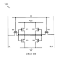
SRAMデバイスは、高性能プロセッサキャッシュなど高速メモリアプリケーションの技術分野で知られている。従来のSRAMセルの構造は通常、4つの相補型金属酸化物半導体電界効果トランジスタ(相補型「MOS」または「CMOS」トランジスタ)から形成されている交差結合された2つのインバータを含む。交差結合されたインバータは、相補的な2進値の「0」および「1」を表す2つの安定状態を有する基本的な記憶素子を形成する。2つのアクセストランジスタが、読取り動作および書込み動作時に記憶素子へのアクセスを制御する働きをする。したがって、従来のSRAMセルアーキテクチャは、6つのトランジスタを含み、一般に6T SRAMセルと呼ばれる。 SRAM devices are known in the technical field of high speed memory applications such as high performance processor caches. Conventional SRAM cell structures typically include two cross-coupled inverters formed from four complementary metal oxide semiconductor field effect transistors (complementary “MOS” or “CMOS” transistors). The cross-coupled inverters form a basic storage element with two stable states representing complementary binary values “0” and “1”. Two access transistors serve to control access to the storage element during read and write operations. Thus, the conventional SRAM cell architecture includes six transistors and is commonly referred to as a 6T SRAM cell.
図1は従来の6T SRAMセル100を示している。この記憶素子は、トランジスタM1〜M4を備える。セル100における書込み動作は、正の電源電圧VDDへの相補的なビット線BLおよびBLB、ならびにワード線WLを介して0または1を駆動することによって開始している。アクセストランジスタM5およびM6が、相補的なビット線上の値を記憶素子に書き込む。読取り動作時には、相補的なビット線BLおよびBLBがどちらも、事前に定められた値、通常はVDDにプリチャージされる。ワード線WLがアクティブ化されると、記憶素子に記憶されている相補的な値が一方の相補的なビット線、たとえばBLを放電させるように働き、一方、他方の相補的なビット線BLBはプリチャージ電圧に維持される。センス増幅器(図示せず)は、放出されたビット線BLおよびプリチャージされた相補的なビット線BLBの微分値を迅速に検出し、それに応じて0を読み出す。
FIG. 1 shows a conventional
ナノメートル技術でデバイスサイズが小さくなることにより、従来の6T SRAMセル100において使用されるMOSトランジスタは、性能の目標を満たすことへのますます高まる要求の影響を受けている。しかしながら、SRAM回路は、消費電力を低減するために、低い動作電圧に抑制される。ランダムなドーピング変動は、低い動作電圧でSRAMセルの動作を制限する。小さいデバイスサイズと低い動作電圧との組合せによって、SRAMなどのメモリデバイスは、処理システムにおける他の論理回路の速度およびパフォーマンスメトリックに遅れをとる。
As device sizes are reduced with nanometer technology, the MOS transistors used in the conventional
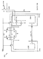
6T SRAMの上記の制限を克服する1つの手法は、SRAMセルのための8トランジスタ(8T)構成を含む。図2は従来の8T SRAMセル200を示している。図示のように、読取りアクセス動作中に性能を向上させるために、たとえば6T SRAMセル100などの6T SRAMセル回路に、トランジスタM7およびM8が追加される。したがって、8つのトランジスタM1〜M8が8T SRAMセル200を形成する。書込み動作中に、書込みワード線WWLが有効にされる。書込みワード線WWL、ならびに相補的な書込みビット線WBLおよびWBLBは、書込みアクセストランジスタM5およびM6を介して記憶素子(トランジスタM1〜M4)に結合される。読取り動作中に、読取りワード線RWLが有効にされ、読取りアクセストランジスタM7およびM8は、記憶素子を読取りビット線RBLに結合する。したがって、6T SRAMセル100とは対照的に、8T SRAMセル200は、読取り動作および書込み動作中に、記憶素子への別個のアクセス経路を提供する。
One approach to overcoming the above limitations of 6T SRAM involves an 8-transistor (8T) configuration for SRAM cells. FIG. 2 shows a conventional
プリチャージトランジスタM9、M10、およびM11は、書込みビット線WBLおよびWBLB、ならびに読取りビット線RBLにプリチャージするように構成される。書込みビット線および読取りビット線は、8T SRAMセル200が非アクティブであるとき、またはスリープモードであるとき、プリチャージされる。このように8T SRAMセル200をプリチャージすることは、上記で説明したように、6T SRAMでの低い動作電圧および低い性能に関連する制限のうちのいくつかを克服する。
Precharge transistors M9, M10, and M11 are configured to precharge write bit lines WBL and WBLB and read bit line RBL. The write and read bit lines are precharged when the
しかしながら、たとえば8T SRAMセル200など8T SRAMセルの従来の実装は、さらなる欠点がある。たとえば、8T SRAMセル200の漏れ電流は、6T SRAMセル100の漏れ電流よりもはるかに高い。プリチャージトランジスタM9、M10、およびM11は、書込みおよび読取りビット線をプリチャージするために構成されるので、これらのプリチャージトランジスタは、8T SRAMセル200が非アクティブであるとき、またはスタンバイモードであるとき、常にオンにされる。その結果、これらのプリチャージトランジスタによって、図示のように、漏れ経路202、204、および206が生じる。書込みビット線WBLをプリチャージすることにより起こる漏れ経路202は、図示のように、トランジスタM9、M5、およびM3を通って、VDDから地面まで形成される。同様に、書込みビット線WBLをプリチャージすることにより起こる漏れ経路204は、トランジスタM10、M6、およびM4を通って、VDDから地面まで形成される。最後に、読取りビット線RBLをプリチャージすることにより起こる漏れ経路206は、トランジスタM11、M7、およびM8を通って、VDDから地面まで形成される。
However, conventional implementations of 8T SRAM cells, such as
漏れ経路202、204、および206は、電力の浪費および性能劣化を招く。したがって、当技術分野では、従来の8T SRAMの実装の上述の欠点を克服する8T SRAMセルの設計が必要である。
Leak
本発明の例示的な実施形態は、たとえば8T SRAMセルなどのメモリセルを含むメモリアレイにおける漏れ電流および消費電力を低減するためのシステムおよび方法を対象とする。 Exemplary embodiments of the present invention are directed to systems and methods for reducing leakage current and power consumption in memory arrays that include memory cells, such as 8T SRAM cells, for example.
たとえば、例示的な実施形態は、メモリアレイにおけるアクセス電力を低減するための方法を対象とし、この方法は、メモリアレイにおけるメモリセルの一群を動的に省電力状態にするステップと、メモリセルの選択された一群を、選択されたメモリセルにおけるアクセス動作中に、動的に有効にするステップとを含む。 For example, exemplary embodiments are directed to a method for reducing access power in a memory array, the method dynamically placing a group of memory cells in a memory array into a power saving state; Dynamically enabling a selected group during an access operation in the selected memory cell.
別の例示的な実施形態は、メモリアレイにおけるアクセス電力を低減するための方法を対象とし、この方法は、書込み回路を動的に省電力状態にするステップと、書込み要求に応答して書込み回路を動的に有効または無効にするステップとを含む。 Another exemplary embodiment is directed to a method for reducing access power in a memory array, the method dynamically placing a write circuit in a power saving state, and a write circuit in response to a write request. Dynamically enabling or disabling.
さらに別の例示的な実施形態は、メモリアレイを対象とし、このメモリアレイは、メモリアレイにおけるメモリセルの一群を動的に省電力状態にするためのロジックと、メモリセルの選択された一群を、選択されたメモリセルにおけるアクセス動作中に、動的に有効にするためのロジックとを含む。 Yet another exemplary embodiment is directed to a memory array that includes logic for dynamically placing a group of memory cells in the memory array into a power saving state and a selected group of memory cells. And logic for enabling dynamically during an access operation in the selected memory cell.
さらなる例示的な実施形態は、メモリアレイを対象とし、このメモリアレイは、書込み回路を動的に省電力状態にするためのロジックと、書込み要求に応答して書込み回路を動的に有効または無効にするためのロジックとを含む。 Further exemplary embodiments are directed to a memory array that dynamically activates or disables a write circuit in response to a write request and logic to dynamically place the write circuit in a power saving state. And logic for
別の例示的な実施形態は、メモリアレイを対象とし、このメモリアレイは、メモリアレイにおけるメモリセルの一群を動的に省電力状態にするための手段と、メモリセルの選択された一群を、選択されたメモリセルにおけるアクセス動作中に、動的に有効にするための手段とを含む。 Another exemplary embodiment is directed to a memory array that includes means for dynamically putting a group of memory cells in the memory array into a power saving state and a selected group of memory cells. Means for dynamically enabling during an access operation in a selected memory cell.
さらに別の例示的な実施形態は、プロセッサによって実行されると、プロセッサに、メモリアレイにおけるアクセス電力を低減するための動作方法を実施させるコードを備える非一時的コンピュータ可読記憶媒体を対象とし、この非一時的コンピュータ可読記憶媒体は、メモリアレイにおけるメモリセルの一群を動的に省電力状態にするためのコードと、メモリセルの選択された一群を、選択されたメモリセルにおけるアクセス動作中に、動的に有効にするためのコードとを含む。 Yet another exemplary embodiment is directed to a non-transitory computer readable storage medium comprising code that, when executed by a processor, causes the processor to implement a method of operation for reducing access power in a memory array. The non-transitory computer readable storage medium includes code for dynamically putting a group of memory cells in a memory array into a power saving state and a selected group of memory cells during an access operation in the selected memory cell. Including code for enabling it dynamically.
さらなる例示的な実施形態は、メモリアレイにおけるアクセス電力を低減するための方法を対象とし、この方法は、メモリアレイにおけるメモリセルの一群を動的に省電力状態にするためのステップと、メモリセルの選択された一群を、選択されたメモリセルにおけるアクセス動作中に、動的に有効にするためのステップとを含む。 Further exemplary embodiments are directed to a method for reducing access power in a memory array, the method comprising: step for dynamically placing a group of memory cells in a memory array into a power saving state; Dynamically enabling a selected group of the memory cells during an access operation in the selected memory cell.
別の例示的な実施形態は、メモリアレイにおけるアクセス電力を低減するための方法を対象とし、この方法は、書込み回路を動的に省電力状態にするためのステップと、書込み要求に応答して書込み回路を動的に有効または無効にするためのステップとを含む。 Another exemplary embodiment is directed to a method for reducing access power in a memory array, the method responsive to a write request and steps for dynamically putting a write circuit into a power saving state. Dynamically enabling or disabling the write circuit.
添付の図面は、本発明の実施形態の説明を助けるために提示され、実施形態の限定ではなく、実施形態の例示のためのみに提供される。 The accompanying drawings are presented to aid in the description of embodiments of the invention and are provided for illustration of the embodiments only, not limitation of the embodiments.
本発明の特定の実施形態を対象とする以下の説明および関連する図面で、本発明の態様を開示する。本発明の範囲から逸脱することなく代替的な実施形態を考案することができる。さらに、本発明の関連する詳細を不明瞭にしないように、本発明のよく知られている要素は詳細に説明されないか、または省略される。 Aspects of the invention are disclosed in the following description and related drawings directed to specific embodiments of the invention. Alternate embodiments may be devised without departing from the scope of the invention. Furthermore, well-known elements of the invention will not be described in detail or will be omitted so as not to obscure the relevant details of the invention.
「例示的な」という語は、「例、事例または実例としての役割を果たすこと」を意味するように本明細書において用いられている。「例示的な」として本明細書で説明する任意の実施形態は、必ずしも他の実施形態よりも好ましいか、または有利であると解釈されるべきではない。同様に、「本発明の実施形態」という用語は、本発明のすべての実施形態が、論じられた特徴、利点または動作モードを含むことを必要としない。 The word “exemplary” is used herein to mean “serving as an example, instance, or illustration”. Any embodiment described herein as "exemplary" is not necessarily to be construed as preferred or advantageous over other embodiments. Similarly, the term “embodiments of the present invention” does not require that all embodiments of the present invention include the discussed features, advantages or modes of operation.
本明細書で使用される用語は、特定の実施形態の説明のみを目的とするものであり、本発明の実施形態を限定するものではない。本明細書で使用する場合、単数形「a」、「an」、および「the」は、文脈が別段に明確に示すのでなければ、複数形をも含むものとする。さらに、「備える(comprises)」、「備えている(comprising)」、「含む(includes)」、および/または「含んでいる(including)」という用語は、本明細書で使用されると、述べられた特徴、整数、ステップ、動作、要素、および/または構成要素の存在を明示するが、1つもしくは複数の他の特徴、整数、ステップ、動作、要素、構成要素、および/またはそれらのグループの存在または追加を排除しないことが理解されよう。 The terminology used herein is for the purpose of describing particular embodiments only and is not intended to be limiting of embodiments of the invention. As used herein, the singular forms “a”, “an”, and “the” are intended to include the plural forms as well, unless the context clearly indicates otherwise. Further, the terms `` comprises '', `` comprising '', `` includes '', and / or `` including '' are used as used herein. The presence of one or more other features, integers, steps, actions, elements, components, and / or groups thereof It will be understood that the presence or addition of is not excluded.
さらに、多くの実施形態が、たとえばコンピューティングデバイスの要素によって実行すべき、一連のアクションに関して説明される。本明細書で説明する様々なアクションは、特定の回路(たとえば、特定用途向け集積回路(ASIC))によって、1つまたは複数のプロセッサによって実行されるプログラム命令によって、あるいは両方の組合せによって実行され得ることを認識されよう。さらに、本明細書で説明するこれらの一連のアクションは、実行時に、関連するプロセッサに本明細書で説明する機能を実行させるコンピュータ命令の対応するセットを記憶した、任意の形式のコンピュータ可読記憶媒体内で全体として具現化されるものと見なすことができる。したがって、本発明の様々な態様は、特許請求する主題の範囲内にすべて入ることが企図されているいくつかの異なる形式で具現化され得る。加えて、本明細書で説明する実施形態ごとに、任意のそのような実施形態の対応する形式について、本明細書では、たとえば、記載のアクションを実行する「ように構成された論理」として説明することがある。 Moreover, many embodiments are described in terms of a series of actions to be performed by, for example, elements of a computing device. The various actions described herein may be performed by particular circuits (e.g., application specific integrated circuits (ASICs)), by program instructions executed by one or more processors, or a combination of both. I will recognize that. Further, these series of actions described herein may be any form of computer readable storage medium that, when executed, stores a corresponding set of computer instructions that cause an associated processor to perform the functions described herein. It can be regarded as embodied as a whole. Thus, various aspects of the invention may be embodied in a number of different forms that are all intended to fall within the scope of the claimed subject matter. In addition, for each embodiment described herein, the corresponding form of any such embodiment is described herein as, for example, "logic configured to" perform the actions described. There are things to do.
例示的な実施形態は、読取りおよび書込みなどのメモリアクセス動作中に漏れ電力が低減され、性能が向上するメモリデバイスを対象とする。実施形態は、たとえば非アクティブ状態中に漏れが少なく、アクセス動作中に動的に有効化するために構成された8T SRAMセル構造などの例示的なメモリデバイスを含み得る。以下で詳細に説明するように、実施形態は、例示的なメモリデバイスの読取りポート部分に動作可能に結合されたフローティングしている読取りビット線を含み得、メモリデバイスが非アクティブ状態であるとき、読取りビット線は、フローティングすることができ、アクセス動作の前および後にプリチャージされ得る。同じく以下で詳細に説明するように、実施形態は、漏れ電流経路が事実上除去され得るように、メモリデバイスの非アクティブ状態中に、書込みビット線をフローティングするように構成されたトライステート書込みドライバ回路およびフローティングしている書込みビット線も含み得る。 Exemplary embodiments are directed to memory devices that have reduced leakage power and improved performance during memory access operations such as reads and writes. Embodiments may include exemplary memory devices, such as an 8T SRAM cell structure that is configured to be dynamically enabled during access operations, for example, with low leakage during inactive states. As described in detail below, embodiments may include a floating read bit line operably coupled to the read port portion of the exemplary memory device, when the memory device is in an inactive state. The read bit line can be floated and can be precharged before and after the access operation. As also described in detail below, embodiments provide a tri-state write driver configured to float a write bit line during an inactive state of a memory device so that a leakage current path can be effectively eliminated. Circuitry and floating write bit lines may also be included.
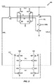
次に図3を参照すると、例示的な8T SRAMセル300が示される。従来の8T SRAMセル200と比較して、8T SRAMセル300の構造では、書込みビット線WBLおよびWBLBに結合されたプリチャージトランジスタM9およびM10を除外することができる。前記のように、プリチャージトランジスタM9およびM10は、8T SRAMセル200における漏れ経路202および204の形成に貢献する。したがって、これらのプリチャージトランジスタM9およびM10の除去は、書込みビット線のプリチャージにより起こる202および204などの漏れ経路を事実上除去し得る。
Referring now to FIG. 3, an exemplary
引き続き図3を参照すると、たとえばM9およびM10などのプリチャージトランジスタの代わりに、トライステート書込みドライバ302が8T SRAM300に導入され得る。トライステート書込みドライバ302は、図示のように、トランジスタM30〜M37を備え得る。図示の実施形態では、トランジスタM30〜M33は、pチャネルMOS(PMOS)トランジスタであり得、一方、トランジスタM34〜M37は、nチャネルMOS(NMOS)トランジスタであり得る。したがって、8T SRAM300が非アクティブ状態であるとき、ネットWCは、高状態(または電圧VDDまたは論理「1」)に駆動され得、それによってPMOSトランジスタM32およびM33がオフにされる。同様に、ネットWTは、低状態(または接地電圧または論理「0」)に駆動され得、それによってNMOSトランジスタM34およびM35もオフにされる。その結果、書込みビット線WBLおよびWBLBへの伝導経路がなく、それによって、それらがフローティングする。このように、ネットWCおよびWTの電圧を制御することによって、VDDから接地電圧への漏れ経路が事実上除去され得る。
With continued reference to FIG. 3, a
8T SRAMがアクティブバンクまたはセットの書込みアクティブ状態であるとき、書込みビット線WBLおよびWBLBは、PMOSトランジスタM30〜M33を介して高状態に駆動され得る。本明細書で使用する場合、「サブバンク」または「セット」は、独立して制御され得るメモリアレイバンクのセクションを指し、独立して有効または無効にされ得る。書込み動作中、ネットWCおよび相補的なネットDCまたはDTを低状態に駆動することによって、PMOSトランジスタM30〜M33は、オンにされ、導通状態になり得る。また、相補的なネットDCおよびDTはNMOSトランジスタM36およびM37のゲートに結合されるので、これらのネットうちの一方を低く駆動することにも、それぞれNMOSトランジスタM36またはM37をオフにする効果がある。しかしながら、8T SRAMが非アクティブなバンクまたはセットにあるとき、書込みビット線はフローティングすることができる。したがって、ネットWCおよびWTの電圧をそれぞれ高状態および低状態に駆動することによって、(図2に示すように)VDDから地面への202のような漏れ経路が事実上除去され得る。 When the 8T SRAM is in the active bank or set write active state, the write bit lines WBL and WBLB can be driven high through PMOS transistors M30-M33. As used herein, a “subbank” or “set” refers to a section of a memory array bank that can be independently controlled and can be independently enabled or disabled. By driving net WC and complementary net DC or DT to a low state during a write operation, PMOS transistors M30-M33 can be turned on and become conductive. Also, since complementary nets DC and DT are coupled to the gates of NMOS transistors M36 and M37, driving one of these nets low also has the effect of turning off NMOS transistor M36 or M37, respectively. . However, the write bit line can float when the 8T SRAM is in an inactive bank or set. Thus, by driving the voltages on nets WC and WT to the high and low states, respectively, a leakage path such as 202 from VDD to ground can be virtually eliminated (as shown in FIG. 2).
8T SRAMセル300の例示的な実装形態はまた、(図2に示すように)読取りビット線をプリチャージすることにより起こる206などの漏れ経路を事実上除去するように構成され得る。読取りビット線のプリチャージからのそのような漏れ経路を除去するために、実施形態は、8T SRAMセル300の非アクティブ状態中、読取りビット線RBLをフローティングするように構成されるロジックを含み得る。ロジックは、8T SRAMセル300においてアクセス動作が実行される前および後に読取りビット線RBLをプリチャージするようにさらに構成され得る。8T SRAMセル300などのセルを備えるSRAMアレイにおける読取りビット線を選択的および動的にフローティングするためのそのようなロジックを実装することについてのさらなる詳細について、以下のセクションで論じる。
An exemplary implementation of
次に図4A〜図4Bを併せて参照すると、例示的なSRAMメモリアレイバンク、バンク400におけるフローティングしている読取りビット線を実施するための例示的な回路が示される。図示の実施形態では、バンク400は、メモリシステムのいくつかのメモリアレイバンクのうちの1つでもよい。バンク400は、4つのセット、SET0〜3に分割されるが、簡潔のために、SET0およびSET3のみが図4Aに示される。図4Bは、SET0およびSET3の拡大図を提供する。バンク400は、128行および144列の8T SRAMセルを含み、SET0〜3の各々は、32行および144列を含む。図示の実施形態は、上記のように、4つのセットに区分されるバンク400を対象としているが、例示的な実施形態は、必ずしもそのような区分に限定されるとは限らない。開示された技法は、バンク、セット、または当技術分野で知られている他の形の区分を含むメモリシステムに容易に拡張することができる。
4A-4B, an exemplary circuit for implementing an exemplary SRAM memory array bank, floating read bit line in
引き続き図4Aを参照すると、制御信号SET_SELECT[3:0]は、バンク400の4つのセットのうちの1つを有効にするために使用されるワンホット信号として構成され得る。図4Bに示すように、SET0は行31:0を備え、SET3は行127:96を備える。
With continued reference to FIG. 4A, the control signal SET_SELECT [3: 0] may be configured as a one-hot signal used to enable one of the four sets of the
以下の制御信号は、図4Bに示すように、SET3を参照して説明しているが、同様の説明がSET0〜2に当てはまることを理解されよう。SET3の選択された行における書込みおよび読取り動作中に8T SRAMセルを有効にするための書込みワード線wwl[127:96]、および読取りワード線rwl[127:96]は、行方向に配置され得る。8T SRAMセルごとの相補的な書込みビット線wblおよびwblbは、列方向に配置された書込み回路から導出され得る。読取りビット線は、制御信号rbl_s3[143:0]から導出され得る。読取りビット線rbl_s3[143:0]は、SET3が選択されるときのみそれらが有効にされ、対応する8T SRAMセルが非アクティブであり、SET3が非選択であるとき、フローティングしているように構成され得る。さらに、読取りビット線rbl_s3[143:0]は、アクセス動作の前および後に、選択された8T SRAMセルがプリチャージされ得るように構成され得る。バンク400において動作可能な制御信号のさらに詳細な動作が、図5に示したタイミング図により以下で提供される。
The following control signals have been described with reference to SET3 as shown in FIG. 4B, but it will be understood that the same description applies to SET0-2. A write word line wwl [127: 96] and a read word line rwl [127: 96] for enabling the 8T SRAM cell during write and read operations in the selected row of SET3 can be arranged in the row direction. . Complementary write bit lines wbl and wblb for each 8T SRAM cell can be derived from a write circuit arranged in the column direction. The read bit line can be derived from the control signal rbl_s3 [143: 0]. Read bit lines rbl_s3 [143: 0] are configured so that they are only enabled when SET3 is selected, the corresponding 8T SRAM cells are inactive, and floating when SET3 is deselected Can be done. Further, the read bit line rbl_s3 [143: 0] can be configured such that the selected 8T SRAM cell can be precharged before and after the access operation. A more detailed operation of the control signals operable in the
図5のタイミング図は、SRAMアレイ400をクロック制御するために使用されるクロック信号CLKを示す。制御信号bank_rbl_pchは、プリチャージ動作を制御するために構成され得る。ワンホット制御信号SET_SELECT[3:0]は、bank_rbl_pchの到着より前に利用可能となり得る。信号rd_force_blpchは、テスト動作モードに対応し、アクティブモード中、低く設定され得る。したがって、アクティブ動作モード中にSET3が選択されることが要求されるとき、SET_SELECT[3]はハイ、SET_SELECT[2:0]テストピンrd_force_blchはローである。対応して、ゲートNOR3およびOR6によって、bank_rbl_pchは、セットSET0〜2ではなく、選択されたSET3のみの読取りビット線rbl_s3[143:0]をプリチャージするために、ゲート制御された信号set3_rbl_pchに伝搬することができる。一例では、読取り動作中に、SET3における特定の8T SRAMセルにアクセスされたとき、対応する読取りワード線RWLはハイである。図5のタイミング図に示すように、ゲート制御された信号set3_rbl_pchは、読取りワード線RWLの持続時間の前および後にオンとなる。したがって、アクティブ動作モード中に、ゲート制御された信号set3_rbl_pchは、上記のように、アクセス動作の前および後に、選択された読取りビット線をプリチャージするように構成され得る。非選択のセット、SET0で以下で詳述するように、対応する読取りビット線は、非アクティブモード中、フローティングすることができる。
The timing diagram of FIG. 5 shows a clock signal CLK that is used to clock the
SET3が有効にされる上記の例を続けると、SET0〜2のワンホット制御信号はローである。したがって、再び図4A〜図4Bを参照すると、信号set0_clampおよびset0_rbl_pchは、ゲートNOR1およびOR5を介してハイである。信号set0_rbl_pchは、(図2のPMOSトランジスタM11と同様の)PMOSトランジスタMS0[143:0]を切断するように動作し、したがって、対応する読取りビット線rbl_s0[143:0]は、フローティングすることができる。このようにして、非選択のセット0〜2では、読取りビット線は、フローティングすることができ、したがって、漏れ経路が連続的にプリチャージするのを防止する。さらに、読取りビット線をフローティングすることによって生じる未知状態が下流の回路に伝搬するのを防止するために、信号set0_clampはハイであり、制御信号OR_S0[143:0]の出力をローの状態にクランプする。明示的に図示されていないが、信号set1_clamp、set2_clampは、制御信号OR_S1[143:0]およびOR_S2[143:0]の出力もローの状態にクランプする。対照的に、選択されたSET3のset3_clampはローであり、非選択のSET2のOR_S2[143:0]の出力はローなので、信号rbl_s3[143:0]は、図示のように、信号rbl_s23[143:0]を介して下流の回路に伝搬することができる。 Continuing the above example where SET3 is enabled, the one-hot control signals for SET0-2 are low. Therefore, referring again to FIGS. 4A-4B, signals set0_clamp and set0_rbl_pch are high through gates NOR1 and OR5. The signal set0_rbl_pch operates to disconnect the PMOS transistor MS0 [143: 0] (similar to the PMOS transistor M11 in FIG. 2), and therefore the corresponding read bit line rbl_s0 [143: 0] can float. it can. In this way, in the unselected sets 0-2, the read bit line can float, thus preventing the leakage path from being continuously precharged. In addition, the set0_clamp signal is high and the output of the control signal OR_S0 [143: 0] is clamped low to prevent unknown states caused by floating the read bit line from propagating to downstream circuits. To do. Although not explicitly shown, the signals set1_clamp and set2_clamp also clamp the outputs of the control signals OR_S1 [143: 0] and OR_S2 [143: 0] to a low state. In contrast, since the set3_clamp of the selected SET3 is low and the output of the unselected SET2 OR_S2 [143: 0] is low, the signal rbl_s3 [143: 0] is, as shown, the signal rbl_s23 [143 : 0] to the downstream circuit.
次に図6〜図7を併せて参照すると、4つのSRAMアレイバンクBANK0〜3を備えるメモリシステム600が示される。4つのSRAMアレイバンク、BANK0〜3の各々は、たとえば図4A〜図4Bのバンク400など、SRAMアレイから形成され得る。したがって、バンク400の場合のように、バンクBANK0〜3の各々は、4つのセットSET0〜3を各々備え得る。バンクBANK0〜3は、ライトスリープモードまたは非アクティブ状態のために構成され得、バンクBANK0〜3のうちのいずれも、またセットSET0〜3のうちのいずれもアクティブではない。バンク400と同様に、バンクBANK0〜3のセットSET0〜3を有効にするために、制御信号set_select[3:0]が使用され得る。バンクBANK0〜3をライトスリープモードにするために、信号mem_light_sleepが使用され得る。
Referring now to FIGS. 6-7, there is shown a
図7を参照すると、図6のラッチLatch0〜3において使用され得るラッチ700の回路実装が示される。信号mem_light_sleepは、リセットピンに結合され得、ラッチ700のNMOSトランジスタ70のゲートを制御する。次に、mem_light_sleepがハイのとき、ラッチ700の内部ノードTは、強制的にローの状態にされ得る。したがって、ラッチ700のset_select出力は、強制的にローの状態にされ得る。
Referring to FIG. 7, a circuit implementation of a
したがって、図6を参照すると、すべての4つのバンクBANK0〜3がライトスリープモードであるとき、すべてのワンホット信号set_select[3:0]が強制的にローになり得る。図4A〜図4Bのバンク400に関して説明したように、制御信号SET_SELECT[3:0]のすべてを強制的にローの状態にすることによって、それぞれSET0〜3に対応するすべての読取りビット線rbl_s3[143:0]、rbl_s2[143:0]、rbl_s1[143:0]、およびrbl_s0[143:0]をフローティングさせる。したがって、バンク400がライトスリープモードであり、セットSET0〜3が非アクティブであるとき、漏れ電流(たとえば、図2のPMOSトランジスタM11を通る)は除去され得る。同様に、図6のメモリシステム600におけるset_select[3:0]を強制的にすることには、バンクBANK0〜3(図示せず)の読取りビット線をフローティングさせる効果があり得、したがって、漏れ電流が除去される。このように、バンクBANK0〜3を備えるメモリシステム600の例示的な8T SRAMセルにおいて、消費電力が最小化され得る。
Therefore, referring to FIG. 6, when all four banks BANK0-3 are in the light sleep mode, all one-hot signals set_select [3: 0] can be forced low. As described with respect to
実施形態は、本明細書で開示するプロセス、機能および/またはアルゴリズムを実行するための様々な方法を含むことが諒解されよう。たとえば、図8に示すように、一実施形態は、たとえばバンク400など、メモリアレイにおける消費電力を低減するための方法を含み得、この方法は、(ブロック802で、たとえば、信号SET_SELECT[3]を制御することによって)メモリアレイにおけるメモリセルの一群(たとえば、図4A〜図4Bに示すように、8T SRAMセルを備えるSET3)を動的に省電力状態にするステップと、(ブロック804で、たとえば、それぞれ読取りおよび書込み動作中に、上記で説明したように、SET_SELECT[3]ならびに読取りおよび書込みワード線およびビット線を制御することによって、SET3を有効にするなど)メモリセルの選択された一群を、メモリセルの選択された一群におけるアクセス動作中に、動的に有効にするステップとを含む。
It will be appreciated that embodiments include various methods for performing the processes, functions and / or algorithms disclosed herein. For example, as shown in FIG. 8, one embodiment may include a method for reducing power consumption in a memory array, such as
さらに、上記実施形態は、たとえば例示的な8T SRAMセル300における読取りおよび書込みワード線およびビット線に結合されたポートなど、単一の読取りポートおよび単一の書込みポートを参照しながら説明したが、実施形態は、単一の読取りまたは書込みポートに限定されない。本明細書で説明する技法は、2つ以上の読取りポートおよび/または2つ以上の書込みポートに容易に拡張され得る。たとえば、図9を参照すると、2つの読取りポートおよび2つの書込みポートを有する例示的な12T SRAMセル900が示される。12T SRAMセル900は、8T SRAMセル300を参照しながら説明した要素を全体的に保持すると同時に、追加の読取りポートおよび追加の書込みポートを追加する。
Further, while the above embodiments have been described with reference to a single read port and a single write port, such as ports coupled to read and write word lines and bit lines in the exemplary
引き続き図9を参照すると、12T SRAMセル900では、図3の8T SRAMセル300に示される素子に加えて、トランジスタM7'およびM8'が導入される。トランジスタM7'およびM8'は、追加の読取りポート(図示せず)をサポートするために、読取りビット線RBL'および読取りワード線RWL'に結合され得る。同様に、書込みワード線WWL'ならびに相補的な書込みビット線WBL'およびWBLB'に結合されたトランジスタM5'およびM6'は、追加の書込みポートをサポートすることができる。8T SRAMセル300を参照しながら説明した読取りビット線RBLと同様に、読取りビット線RBL'は、12T SRAMセル900の非アクティブ状態中にフローティングするように構成され得、したがって、図2に示す206などの漏れ経路が除去される。同様に、相補的な書込みビット線WBLおよびWBLBと同様に、たとえばトライステート書込みドライバ302などのトライステート書込みドライバは、トランジスタM5'およびM6'により起こる202および204などの漏れ経路を除去するために使用され得る。同様に、漏れ経路を除去するための技法は、任意の数の追加の読取りまたは書込みポートに拡張され得る。したがって、例示的な実施形態は、2つ以上の読取りポートおよび/または2つ以上の書込みポートを有する12T SRAMセルについての漏れ経路を除去することができる。
Still referring to FIG. 9, in the
情報および信号は、多種多様な技術および技法のいずれかを使用して表すことができることを当業者は諒解されよう。たとえば、上記の説明全体にわたって言及され得るデータ、命令、コマンド、情報、信号、ビット、シンボル、およびチップは、電圧、電流、電磁波、磁界または磁性粒子、光場または光学粒子、あるいはそれらの任意の組合せによって表され得る。 Those of skill in the art will appreciate that information and signals can be represented using any of a wide variety of techniques and techniques. For example, data, instructions, commands, information, signals, bits, symbols, and chips that may be referred to throughout the above description are voltages, currents, electromagnetic waves, magnetic fields or magnetic particles, light fields or optical particles, or any of them Can be represented by a combination.
さらに、本明細書で開示した実施形態に関連して説明した様々な例示的な論理ブロック、モジュール、回路、およびアルゴリズムステップは、電子ハードウェア、コンピュータソフトウェア、または両方の組合せとして実装できることを、当業者は諒解されよう。ハードウェアとソフトウェアのこの互換性を明確に示すために、様々な例示的な構成要素、ブロック、モジュール、回路、およびステップを、上記では概してそれらの機能に関して説明した。そのような機能をハードウェアとして実装するか、ソフトウェアとして実装するかは、特定の適用例および全体的なシステムに課される設計制約に依存する。当業者は、説明した機能を特定の適用例ごとに様々な方法で実装し得るが、そのような実装の決定は、本発明の範囲からの逸脱を生じるものと解釈すべきではない。 Further, it is understood that the various exemplary logic blocks, modules, circuits, and algorithm steps described in connection with the embodiments disclosed herein can be implemented as electronic hardware, computer software, or a combination of both. The contractor will be understood. To clearly illustrate this interchangeability of hardware and software, various illustrative components, blocks, modules, circuits, and steps have been described above generally in terms of their functionality. Whether such functionality is implemented as hardware or software depends upon the particular application and design constraints imposed on the overall system. Those skilled in the art may implement the described functionality in a variety of ways for each particular application, but such implementation decisions should not be construed as departing from the scope of the present invention.
本明細書で開示した実施形態と関連して説明した方法、シーケンス、および/またはアルゴリズムは、ハードウェアで、プロセッサによって実行されるソフトウェアモジュールで、またはその2つの組合せで直接具現化され得る。ソフトウェアモジュールは、RAMメモリ、フラッシュメモリ、ROMメモリ、EPROMメモリ、EEPROMメモリ、レジスタ、ハードディスク、リムーバブルディスク、CD-ROM、または当技術分野で知られている任意の他の形態の記憶媒体中に常駐し得る。例示的な記憶媒体は、プロセッサが記憶媒体から情報を読み取り、記憶媒体に情報を書き込むことができるように、プロセッサに結合される。代替として、記憶媒体はプロセッサと一体であり得る。 The methods, sequences, and / or algorithms described in connection with the embodiments disclosed herein may be directly implemented in hardware, software modules executed by a processor, or a combination of the two. Software modules reside in RAM memory, flash memory, ROM memory, EPROM memory, EEPROM memory, registers, hard disks, removable disks, CD-ROMs, or any other form of storage medium known in the art Can do. An exemplary storage medium is coupled to the processor such that the processor can read information from, and write information to, the storage medium. In the alternative, the storage medium may be integral to the processor.
したがって、本発明の実施形態は、メモリアレイにおける消費電力を低減するための方法を具現化するコンピュータ可読媒体を含み得る。したがって、本発明は図示の例に限定されず、本明細書で説明した機能を実行するためのいかなる手段も、本発明の実施形態中に含まれる。 Thus, embodiments of the invention may include a computer readable medium embodying a method for reducing power consumption in a memory array. Accordingly, the present invention is not limited to the illustrated examples, and any means for performing the functions described herein are included in embodiments of the present invention.
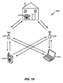
図10は、本開示の一実施形態が有利に使用され得る例示的なワイヤレス通信システム1000を示す。説明のために、図10は、3つの遠隔ユニット1020、1030、および1050ならびに2つの基地局1040を示す。図10では、ワイヤレスローカルループシステムにおいて、遠隔ユニット1020は携帯電話として示され、遠隔ユニット1030はポータブルコンピュータとして示され、遠隔ユニット1050は定位置遠隔ユニットとして示されている。たとえば、遠隔ユニットは、携帯電話、ハンドヘルドパーソナル通信システム(PCS)ユニット、個人情報端末のようなポータブルデータユニット、GPS対応デバイス、ナビゲーションデバイス、セットトップボックス、音楽プレーヤ、ビデオプレーヤ、エンターテインメントユニット、メータ読取り機器のような固定ロケーションデータユニット、またはデータもしくはコンピュータ命令の記憶もしくは取り出しを行う任意の他のデバイス、またはそれらの任意の組合せであってよい。図10は、本開示の教示による遠隔ユニットを示すが、本開示は、これらの例示的な示されたユニットに限定されない。本開示の実施形態は、試験および特徴付けのための、メモリおよびオンチップ回路を含む能動的な集積回路を含む、任意のデバイスにおいて適切に用いられ得る。
FIG. 10 illustrates an example
前述の開示されたデバイスおよび方法は、通常、コンピュータ可読記憶媒体に保存されるGDSIIおよびGERBERコンピュータファイルとなるように、設計され構成される。次いでこれらのファイルは、これらのファイルに基づいてデバイスを製造する製造担当者に与えられる。得られる製品は半導体ウェハであり、このウェハは次いで、半導体ダイに切断され、半導体チップにパッケージングされる。次いで、このチップが、上で説明されたデバイスで利用される。 The aforementioned disclosed devices and methods are typically designed and configured to be GDSII and GERBER computer files stored on computer readable storage media. These files are then provided to the manufacturing personnel who manufacture the device based on these files. The resulting product is a semiconductor wafer, which is then cut into semiconductor dies and packaged into semiconductor chips. This chip is then utilized in the device described above.
上記の開示は本発明の例示的な実施形態を示すが、添付の特許請求の範囲によって規定される本発明の範囲から逸脱することなく、本明細書において様々な変更および修正を行えることに留意されたい。本明細書で説明した本発明の実施形態による方法クレームの機能、ステップおよび/またはアクションは、特定の順序で実行されなくてもよい。さらに、本発明の要素は、単数形で説明または特許請求されていることがあるが、単数形に限定することが明示的に述べられていない限り、複数形が企図される。 While the above disclosure illustrates exemplary embodiments of the present invention, it is noted that various changes and modifications can be made herein without departing from the scope of the present invention as defined by the appended claims. I want to be. The functions, steps and / or actions of a method claim according to embodiments of the invention described herein may not be performed in a particular order. Further, although elements of the invention may be described or claimed in the singular, the plural is contemplated unless expressly stated to be limited to the singular.
70 NMOSトランジスタ
100 6T SRAMセル
200 8T SRAMセル
202 漏れ経路
204 漏れ経路
206 漏れ経路
300 8T SRAMセル
302 トライステート書込みドライバ
400 バンク
400 SRAMアレイ
600 メモリシステム
700 ラッチ
900 12T SRAMセル
1000 ワイヤレス通信システム
1020 遠隔ユニット
1030 遠隔ユニット
1040 基地局
1050 遠隔ユニット
70 NMOS transistor
100 6T SRAM cell
200 8T SRAM cell
202 Leakage path
204 Leakage path
206 Leakage path
300 8T SRAM cell
302 3-state write driver
400 banks
400 SRAM array
600 memory system
700 latch
900 12T SRAM cell
1000 wireless communication system
1020 Remote unit
1030 Remote unit
1040 base station
1050 remote unit
Claims (27)
前記メモリアレイの1つまたは複数のメモリセルの一群に対応する読取りビット線および書込みビット線をフローティングさせることによって、非アクティブ状態中、前記1つまたは複数のメモリセルの一群を動的に省電力状態にするステップであり、前記メモリセルが、8トランジスタスタティックランダムアクセスメモリ(8T SRAM)セルとして形成される、ステップと、
アクセス動作中、前記一群のうちの1つまたは複数の選択されたメモリセルに関連付けられた選択された読取りビット線または前記書込みビット線をプリチャージすることによって、前記1つまたは複数の選択されたメモリセルを動的にアクティブ化するステップと
を含み、
前記書込みビット線は、トライステート書込みドライバを使用してプリチャージまたはフローティングされ、
前記読取りビット線は、ワンホット制御信号を使用してプリチャージまたはフローティングされる、方法。 A method for reducing leakage power in a memory array, comprising:
Dynamically power saving a group of one or more memory cells during an inactive state by floating a read bit line and a write bit line corresponding to the group of one or more memory cells of the memory array The memory cell is formed as an 8-transistor static random access memory (8T SRAM) cell; and
During an access operation, the one or more selected by precharging a selected read bit line or the write bit line associated with one or more selected memory cells of the group. Dynamically activating a memory cell, and
The write bit line is precharged or floating using a tri-state write driver,
The read bit line is precharged or floated using a one-hot control signal.
記憶素子を形成するステップと、
2つの書込みアクセストランジスタを介して、書込みワード線および1対の相補的な書込みビット線を前記記憶素子に結合するステップと、
2つの読取りアクセストランジスタを介して、前記記憶素子を読取りワード線および読取りビット線に結合するステップと
を含む、請求項1に記載の方法。 The step of forming the 8T SRAM cell is
Forming a memory element;
Coupling a write word line and a pair of complementary write bit lines to the storage element via two write access transistors;
The method of claim 1, comprising coupling the storage element to a read word line and a read bit line via two read access transistors.
をさらに含む請求項1に記載の方法。 The method of claim 1, further comprising dynamically enabling or disabling write circuitry of the memory array based on a write request or inactive mode, respectively.
前記メモリアレイの1つまたは複数のメモリセルの一群に対応する読取りビット線および書込みビット線をフローティングさせることによって、非アクティブ状態中、前記1つまたは複数のメモリセルの一群を動的に省電力状態にするための論理手段であり、前記メモリセルが、8トランジスタスタティックランダムアクセスメモリ(8T SRAM)セルとして形成される、論理手段と、
アクセス動作中、前記一群のうちの1つまたは複数の選択されたメモリセルに関連付けられた選択された読取りビット線または前記書込みビット線に印加されるプリチャージに基づき、前記1つまたは複数の選択されたメモリセルを動的にアクティブ化するための論理手段と、
前記書込みビット線をプリチャージまたはフローティングするトライステート書込みドライバと、
前記読取りビット線をプリチャージまたはフローティングするワンホット制御信号と
を含むメモリアレイ。 A memory array,
Dynamically power saving a group of one or more memory cells during an inactive state by floating a read bit line and a write bit line corresponding to the group of one or more memory cells of the memory array Logic means for bringing into state, wherein the memory cell is formed as an 8-transistor static random access memory (8T SRAM) cell; and
The one or more selections based on a precharge applied to a selected read bit line or the write bit line associated with one or more selected memory cells of the group during an access operation. Logic means for dynamically activating activated memory cells;
A tri-state write driver for precharging or floating the write bit line;
And a one-hot control signal for precharging or floating the read bit line.
記憶素子と、
少なくとも1対の書込みアクセストランジスタを介して前記記憶素子に結合されている少なくとも1つの書込みワード線および少なくとも1対の相補型の書込みビット線と、
少なくとも1対の読取りアクセストランジスタを介して前記記憶素子に結合されている少なくとも1つの読取りワード線および少なくとも1つの読取りビット線と
を含む、請求項11に記載のメモリアレイ。 The 8T SRAM cell is
A storage element;
At least one write word line and at least one pair of complementary write bit lines coupled to the storage element via at least one pair of write access transistors;
12. The memory array of claim 11 , comprising at least one read word line and at least one read bit line coupled to the storage element via at least one pair of read access transistors.
を含む請求項11に記載のメモリアレイ。 12. The memory array of claim 11 , comprising logic means for dynamically enabling or disabling a write circuit of the memory array based on a write request or inactive mode, respectively.
前記メモリアレイの1つまたは複数のメモリセルの一群に対応する読取りビット線および書込みビット線をフローティングさせることによって、非アクティブ状態中、前記1つまたは複数のメモリセルの一群を動的に省電力状態にするための手段であり、前記メモリセルが、8トランジスタスタティックランダムアクセスメモリ(8T SRAM)セルとして形成される、手段と、
アクセス動作中、前記一群のうちの1つまたは複数の選択されたメモリセルを動的にアクティブ化するための手段と、
前記書込みビット線をプリチャージまたはフローティングするトライステート書込みドライバと、
前記読取りビット線をプリチャージまたはフローティングするワンホット制御信号と
を含むメモリアレイ。 A memory array,
Dynamically power saving a group of one or more memory cells during an inactive state by floating a read bit line and a write bit line corresponding to the group of one or more memory cells of the memory array Means for providing a state, wherein the memory cell is formed as an 8-transistor static random access memory (8T SRAM) cell;
Means for dynamically activating one or more selected memory cells of the group during an access operation;
A tri-state write driver for precharging or floating the write bit line;
And a one-hot control signal for precharging or floating the read bit line.
前記メモリアレイの1つまたは複数のメモリセルの一群に対応する読取りビット線および書込みビット線をフローティングさせることによって、非アクティブ状態中、前記1つまたは複数のメモリセルの一群を動的に省電力状態にするためのコードであり、前記メモリセルが、8トランジスタスタティックランダムアクセスメモリ(8T SRAM)セルとして形成される、コードと、
アクセス動作中、前記一群のうちの1つまたは複数の選択されたメモリセルに関連付けられた選択された読取りビット線または前記書込みビット線をプリチャージすることによって、前記1つまたは複数の選択されたメモリセルを動的にアクティブ化するためのコードと
を含み、
前記メモリアレイは、
前記書込みビット線をプリチャージまたはフローティングするトライステート書込みドライバと、
前記読取りビット線をプリチャージまたはフローティングするワンホット制御信号と
を含む、非一時的コンピュータ可読記憶媒体。 A non-transitory computer readable storage medium comprising code that, when executed by a processor, causes the processor to perform a method of operation for reducing access power in a memory array,
Dynamically power saving a group of one or more memory cells during an inactive state by floating a read bit line and a write bit line corresponding to the group of one or more memory cells of the memory array A code for placing the memory cell in an 8-transistor static random access memory (8T SRAM) cell;
During an access operation, the one or more selected by precharging a selected read bit line or the write bit line associated with one or more selected memory cells of the group. Including code for dynamically activating memory cells, and
The memory array is
A tri-state write driver for precharging or floating the write bit line;
A non-transitory computer-readable storage medium comprising: a one-hot control signal for precharging or floating the read bit line.
Applications Claiming Priority (3)
| Application Number | Priority Date | Filing Date | Title |
|---|---|---|---|
| US13/249,297 US8824230B2 (en) | 2011-09-30 | 2011-09-30 | Method and apparatus of reducing leakage power in multiple port SRAM memory cell |
| US13/249,297 | 2011-09-30 | ||
| PCT/US2012/058178 WO2013049763A1 (en) | 2011-09-30 | 2012-09-30 | Method and apparatus of reducing leakage power in multiple port sram memory cell |
Publications (3)
| Publication Number | Publication Date |
|---|---|
| JP2014528629A JP2014528629A (en) | 2014-10-27 |
| JP2014528629A5 JP2014528629A5 (en) | 2014-12-04 |
| JP5914671B2 true JP5914671B2 (en) | 2016-05-11 |
Family
ID=47073525
Family Applications (1)
| Application Number | Title | Priority Date | Filing Date |
|---|---|---|---|
| JP2014533456A Active JP5914671B2 (en) | 2011-09-30 | 2012-09-30 | Method and apparatus for reducing leakage power in a multi-port SRAM memory cell |
Country Status (7)
| Country | Link |
|---|---|
| US (1) | US8824230B2 (en) |
| EP (1) | EP2761621B1 (en) |
| JP (1) | JP5914671B2 (en) |
| KR (1) | KR101536233B1 (en) |
| CN (1) | CN103875038B (en) |
| IN (1) | IN2014CN01829A (en) |
| WO (1) | WO2013049763A1 (en) |
Families Citing this family (33)
| Publication number | Priority date | Publication date | Assignee | Title |
|---|---|---|---|---|
| US9093135B2 (en) * | 2012-11-15 | 2015-07-28 | Nvidia Corporation | System, method, and computer program product for implementing a storage array |
| US8947967B2 (en) * | 2012-12-21 | 2015-02-03 | Advanced Micro Devices Inc. | Shared integrated sleep mode regulator for SRAM memory |
| US9007817B2 (en) * | 2013-05-06 | 2015-04-14 | Qualcomm Incorporated | Pre-charging bitlines in a static random access memory (SRAM) prior to data access for reducing leakage power, and related systems and methods |
| US9442675B2 (en) | 2013-05-08 | 2016-09-13 | Qualcomm Incorporated | Redirecting data from a defective data entry in memory to a redundant data entry prior to data access, and related systems and methods |
| US9588573B2 (en) | 2013-10-28 | 2017-03-07 | Globalfoundries Inc. | Reduced-power trace array for a processor |
| US20150310901A1 (en) * | 2014-04-24 | 2015-10-29 | Qualcomm Incorporated | Memory with a sleep mode |
| US9671855B2 (en) * | 2014-06-30 | 2017-06-06 | Micron Technology, Inc. | Apparatuses and methods of entering unselected memories into a different power mode during multi-memory operation |
| CN106030715A (en) * | 2014-09-25 | 2016-10-12 | 克劳帕斯科技有限公司 | Thyristor volatile random access memory and methods of manufacture |
| US9449669B2 (en) | 2014-09-25 | 2016-09-20 | Kilopass Technology, Inc. | Cross-coupled thyristor SRAM circuits and methods of operation |
| US9530482B2 (en) | 2014-09-25 | 2016-12-27 | Kilopass Technology, Inc. | Methods of retaining and refreshing data in a thyristor random access memory |
| US9741413B2 (en) | 2014-09-25 | 2017-08-22 | Kilopass Technology, Inc. | Methods of reading six-transistor cross-coupled thyristor-based SRAM memory cells |
| US9613968B2 (en) | 2014-09-25 | 2017-04-04 | Kilopass Technology, Inc. | Cross-coupled thyristor SRAM semiconductor structures and methods of fabrication |
| US9460771B2 (en) | 2014-09-25 | 2016-10-04 | Kilopass Technology, Inc. | Two-transistor thyristor SRAM circuit and methods of operation |
| US20160093624A1 (en) | 2014-09-25 | 2016-03-31 | Kilopass Technology, Inc. | Thyristor Volatile Random Access Memory and Methods of Manufacture |
| US9564199B2 (en) | 2014-09-25 | 2017-02-07 | Kilopass Technology, Inc. | Methods of reading and writing data in a thyristor random access memory |
| US9564441B2 (en) | 2014-09-25 | 2017-02-07 | Kilopass Technology, Inc. | Two-transistor SRAM semiconductor structure and methods of fabrication |
| US9496021B2 (en) | 2014-09-25 | 2016-11-15 | Kilopass Technology, Inc. | Power reduction in thyristor random access memory |
| EP3149741A4 (en) * | 2014-09-25 | 2018-01-17 | Kilopass Technology, Inc. | Methods of retaining and refreshing data in a thyristor random access memory |
| US9384825B2 (en) * | 2014-09-26 | 2016-07-05 | Qualcomm Incorporated | Multi-port memory circuits |
| US10431269B2 (en) | 2015-02-04 | 2019-10-01 | Altera Corporation | Methods and apparatus for reducing power consumption in memory circuitry by controlling precharge duration |
| KR101674803B1 (en) | 2015-04-17 | 2016-11-22 | 경희대학교 산학협력단 | Memory apparatus and method thereof |
| CN105304123B (en) * | 2015-12-04 | 2018-06-01 | 上海兆芯集成电路有限公司 | Static RAM |
| KR101927583B1 (en) | 2016-04-21 | 2018-12-10 | 연세대학교 산학협력단 | Local Bit Line Sharing Memory Device and Driving Method Thereof |
| US9761304B1 (en) | 2016-09-27 | 2017-09-12 | International Business Machines Corporation | Write-bitline control in multicore SRAM arrays |
| US9837143B1 (en) | 2016-10-12 | 2017-12-05 | International Business Machines Corporation | NAND-based write driver for SRAM |
| US10249362B2 (en) * | 2016-12-06 | 2019-04-02 | Gsi Technology, Inc. | Computational memory cell and processing array device using the memory cells for XOR and XNOR computations |
| KR102021601B1 (en) * | 2017-09-22 | 2019-09-16 | 경북대학교 산학협력단 | Ultra-low voltage memory device and operating method thereof |
| US10762934B2 (en) * | 2018-06-28 | 2020-09-01 | Taiwan Semiconductor Manufacturing Co., Ltd. | Leakage pathway prevention in a memory storage device |
| EP3906555A4 (en) * | 2019-01-05 | 2022-09-21 | Synopsys, Inc. | Enhanced read sensing margin and minimized vdd for sram cell arrays |
| US20190228821A1 (en) * | 2019-03-29 | 2019-07-25 | Intel Corporation | Programmable High-Speed and Low-power Mode FPGA Memory with Configurable Floating Bitlines Scheme |
| WO2022266541A2 (en) * | 2021-06-18 | 2022-12-22 | University Of Southern California | Augmented memory computing: a new pathway for efficient ai computations |
| US20230402092A1 (en) * | 2022-06-08 | 2023-12-14 | Arm Limited | Bitline Precharge Techniques |
| US11940493B1 (en) * | 2022-09-16 | 2024-03-26 | Nvidia Corp. | Flexible one-hot decoding logic for clock controls |
Family Cites Families (21)
| Publication number | Priority date | Publication date | Assignee | Title |
|---|---|---|---|---|
| JP3252666B2 (en) * | 1995-08-14 | 2002-02-04 | 日本電気株式会社 | Semiconductor storage device |
| JPH11261017A (en) * | 1998-03-16 | 1999-09-24 | Fujitsu Ltd | Semiconductor storage device |
| JPH11345486A (en) * | 1998-06-01 | 1999-12-14 | Mitsubishi Electric Corp | Dram provided with self-refresh control circuit and system lsi |
| JP3866594B2 (en) * | 2002-03-15 | 2007-01-10 | Necエレクトロニクス株式会社 | Delay circuit, semiconductor memory device, and control method of semiconductor memory device |
| JP2004095000A (en) * | 2002-08-29 | 2004-03-25 | Fujitsu Ltd | Static semiconductor storage device and its control method |
| JP2004355760A (en) * | 2003-05-30 | 2004-12-16 | Renesas Technology Corp | Data storage circuit |
| US7365432B2 (en) * | 2004-08-23 | 2008-04-29 | Taiwan Semiconductor Manufacturing Company, Ltd. | Memory cell structure |
| US7082073B2 (en) * | 2004-12-03 | 2006-07-25 | Micron Technology, Inc. | System and method for reducing power consumption during extended refresh periods of dynamic random access memory devices |
| US20070242498A1 (en) | 2006-04-13 | 2007-10-18 | Anantha Chandrakasan | Sub-threshold static random access memory |
| US7619916B2 (en) | 2006-07-06 | 2009-11-17 | Stmicroelectronics Pvt. Ltd. | 8-T SRAM cell circuit, system and method for low leakage current |
| US7440313B2 (en) * | 2006-11-17 | 2008-10-21 | Freescale Semiconductor, Inc. | Two-port SRAM having improved write operation |
| WO2008088135A1 (en) * | 2007-01-16 | 2008-07-24 | Chungbuk National University Industry-Academic Cooperation Foundation | Multiple valued dynamic random access memory cell and thereof array using single electron transistor |
| US7564725B2 (en) | 2007-08-31 | 2009-07-21 | Texas Instruments Incorporated | SRAM bias for read and write |
| KR101488166B1 (en) | 2008-03-26 | 2015-02-02 | 삼성전자주식회사 | Static memory device and SRAM with write assist |
| US7791976B2 (en) * | 2008-04-24 | 2010-09-07 | Qualcomm Incorporated | Systems and methods for dynamic power savings in electronic memory operation |
| JP2009295229A (en) * | 2008-06-05 | 2009-12-17 | Toshiba Corp | Semiconductor memory device |
| US7961499B2 (en) | 2009-01-22 | 2011-06-14 | Qualcomm Incorporated | Low leakage high performance static random access memory cell using dual-technology transistors |
| US7986566B2 (en) | 2009-04-01 | 2011-07-26 | Texas Instruments Incorporated | SRAM cell with read buffer controlled for low leakage current |
| US8159863B2 (en) | 2009-05-21 | 2012-04-17 | Texas Instruments Incorporated | 6T SRAM cell with single sided write |
| US8982659B2 (en) | 2009-12-23 | 2015-03-17 | Intel Corporation | Bitline floating during non-access mode for memory arrays |
| JP5621704B2 (en) * | 2011-05-11 | 2014-11-12 | 富士通セミコンダクター株式会社 | Semiconductor memory device |
-
2011
- 2011-09-30 US US13/249,297 patent/US8824230B2/en active Active
-
2012
- 2012-09-30 CN CN201280047908.7A patent/CN103875038B/en active Active
- 2012-09-30 EP EP12777992.4A patent/EP2761621B1/en active Active
- 2012-09-30 IN IN1829CHN2014 patent/IN2014CN01829A/en unknown
- 2012-09-30 JP JP2014533456A patent/JP5914671B2/en active Active
- 2012-09-30 WO PCT/US2012/058178 patent/WO2013049763A1/en active Application Filing
- 2012-09-30 KR KR1020147011835A patent/KR101536233B1/en active IP Right Grant
Also Published As
| Publication number | Publication date |
|---|---|
| CN103875038A (en) | 2014-06-18 |
| JP2014528629A (en) | 2014-10-27 |
| EP2761621B1 (en) | 2023-10-18 |
| EP2761621A1 (en) | 2014-08-06 |
| IN2014CN01829A (en) | 2015-05-29 |
| KR101536233B1 (en) | 2015-07-13 |
| CN103875038B (en) | 2017-05-03 |
| US20130083613A1 (en) | 2013-04-04 |
| KR20140079445A (en) | 2014-06-26 |
| WO2013049763A1 (en) | 2013-04-04 |
| US8824230B2 (en) | 2014-09-02 |
Similar Documents
| Publication | Publication Date | Title |
|---|---|---|
| JP5914671B2 (en) | Method and apparatus for reducing leakage power in a multi-port SRAM memory cell | |
| US10424392B2 (en) | Read-assist circuits for memory bit cells employing a P-type field-effect transistor (PFET) read port(s), and related memory systems and methods | |
| US7492627B2 (en) | Memory with increased write margin bitcells | |
| US7643330B1 (en) | Sequentially-accessed 1R/1W double-pumped single port SRAM with shared decoder architecture | |
| JP6612856B2 (en) | 7-transistor static random access memory bit cell with reduced read disturb | |
| EP2556506B1 (en) | Programmable tracking circuit for tracking semiconductor memory read current | |
| US8947970B2 (en) | Word line driver circuits and methods for SRAM bit cell with reduced bit line pre-charge voltage | |
| WO2008103516A1 (en) | Memory having a dummy bitline for timing control | |
| US10163490B2 (en) | P-type field-effect transistor (PFET)-based sense amplifiers for reading PFET pass-gate memory bit cells, and related memory systems and methods | |
| JP2005025859A (en) | Semiconductor memory device | |
| CN112053713A (en) | Bit line precharge circuit | |
| TW201822201A (en) | Memory device | |
| US20140119100A1 (en) | Sram with improved write operation | |
| Singh et al. | A data aware 9T static random access memory cell for low power consumption and improved stability | |
| US20070291561A1 (en) | Sense-amplifier assist (saa) with power-reduction technique | |
| Golman et al. | Configurable multi-port dynamic bitcell with internal refresh mechanism | |
| US7751267B2 (en) | Half-select compliant memory cell precharge circuit | |
| TWI720360B (en) | Bitline-driven sense amplifier clocking scheme | |
| US20080123437A1 (en) | Apparatus for Floating Bitlines in Static Random Access Memory Arrays |
Legal Events
| Date | Code | Title | Description |
|---|---|---|---|
| A521 | Request for written amendment filed |
Free format text: JAPANESE INTERMEDIATE CODE: A523 Effective date: 20141009 |
|
| A871 | Explanation of circumstances concerning accelerated examination |
Free format text: JAPANESE INTERMEDIATE CODE: A871 Effective date: 20141009 |
|
| A975 | Report on accelerated examination |
Free format text: JAPANESE INTERMEDIATE CODE: A971005 Effective date: 20141027 |
|
| A131 | Notification of reasons for refusal |
Free format text: JAPANESE INTERMEDIATE CODE: A131 Effective date: 20141110 |
|
| A601 | Written request for extension of time |
Free format text: JAPANESE INTERMEDIATE CODE: A601 Effective date: 20150210 |
|
| A521 | Request for written amendment filed |
Free format text: JAPANESE INTERMEDIATE CODE: A523 Effective date: 20150310 |
|
| A131 | Notification of reasons for refusal |
Free format text: JAPANESE INTERMEDIATE CODE: A131 Effective date: 20150406 |
|
| A601 | Written request for extension of time |
Free format text: JAPANESE INTERMEDIATE CODE: A601 Effective date: 20150629 |
|
| A601 | Written request for extension of time |
Free format text: JAPANESE INTERMEDIATE CODE: A601 Effective date: 20150804 |
|
| A521 | Request for written amendment filed |
Free format text: JAPANESE INTERMEDIATE CODE: A523 Effective date: 20150907 |
|
| A02 | Decision of refusal |
Free format text: JAPANESE INTERMEDIATE CODE: A02 Effective date: 20151005 |
|
| A521 | Request for written amendment filed |
Free format text: JAPANESE INTERMEDIATE CODE: A523 Effective date: 20160204 |
|
| A911 | Transfer to examiner for re-examination before appeal (zenchi) |
Free format text: JAPANESE INTERMEDIATE CODE: A911 Effective date: 20160215 |
|
| TRDD | Decision of grant or rejection written | ||
| A01 | Written decision to grant a patent or to grant a registration (utility model) |
Free format text: JAPANESE INTERMEDIATE CODE: A01 Effective date: 20160307 |
|
| A61 | First payment of annual fees (during grant procedure) |
Free format text: JAPANESE INTERMEDIATE CODE: A61 Effective date: 20160404 |
|
| R150 | Certificate of patent or registration of utility model |
Ref document number: 5914671 Country of ref document: JP Free format text: JAPANESE INTERMEDIATE CODE: R150 |
|
| R250 | Receipt of annual fees |
Free format text: JAPANESE INTERMEDIATE CODE: R250 |
|
| R250 | Receipt of annual fees |
Free format text: JAPANESE INTERMEDIATE CODE: R250 |
|
| R250 | Receipt of annual fees |
Free format text: JAPANESE INTERMEDIATE CODE: R250 |
|
| R250 | Receipt of annual fees |
Free format text: JAPANESE INTERMEDIATE CODE: R250 |
|
| R250 | Receipt of annual fees |
Free format text: JAPANESE INTERMEDIATE CODE: R250 |
|
| R250 | Receipt of annual fees |
Free format text: JAPANESE INTERMEDIATE CODE: R250 |