JP5909660B2 - Wiring board - Google Patents
Wiring board Download PDFInfo
- Publication number
- JP5909660B2 JP5909660B2 JP2013546502A JP2013546502A JP5909660B2 JP 5909660 B2 JP5909660 B2 JP 5909660B2 JP 2013546502 A JP2013546502 A JP 2013546502A JP 2013546502 A JP2013546502 A JP 2013546502A JP 5909660 B2 JP5909660 B2 JP 5909660B2
- Authority
- JP
- Japan
- Prior art keywords
- long hole
- long
- hole row
- wiring board
- solder
- Prior art date
- Legal status (The legal status is an assumption and is not a legal conclusion. Google has not performed a legal analysis and makes no representation as to the accuracy of the status listed.)
- Expired - Fee Related
Links
Images


Classifications
-
- H—ELECTRICITY
- H05—ELECTRIC TECHNIQUES NOT OTHERWISE PROVIDED FOR
- H05K—PRINTED CIRCUITS; CASINGS OR CONSTRUCTIONAL DETAILS OF ELECTRIC APPARATUS; MANUFACTURE OF ASSEMBLAGES OF ELECTRICAL COMPONENTS
- H05K1/00—Printed circuits
- H05K1/02—Details
- H05K1/0213—Electrical arrangements not otherwise provided for
- H05K1/0263—High current adaptations, e.g. printed high current conductors or using auxiliary non-printed means; Fine and coarse circuit patterns on one circuit board
-
- H—ELECTRICITY
- H05—ELECTRIC TECHNIQUES NOT OTHERWISE PROVIDED FOR
- H05K—PRINTED CIRCUITS; CASINGS OR CONSTRUCTIONAL DETAILS OF ELECTRIC APPARATUS; MANUFACTURE OF ASSEMBLAGES OF ELECTRICAL COMPONENTS
- H05K2201/00—Indexing scheme relating to printed circuits covered by H05K1/00
- H05K2201/03—Conductive materials
- H05K2201/0302—Properties and characteristics in general
- H05K2201/0305—Solder used for other purposes than connections between PCB or components, e.g. for filling vias or for programmable patterns
-
- H—ELECTRICITY
- H05—ELECTRIC TECHNIQUES NOT OTHERWISE PROVIDED FOR
- H05K—PRINTED CIRCUITS; CASINGS OR CONSTRUCTIONAL DETAILS OF ELECTRIC APPARATUS; MANUFACTURE OF ASSEMBLAGES OF ELECTRICAL COMPONENTS
- H05K2201/00—Indexing scheme relating to printed circuits covered by H05K1/00
- H05K2201/10—Details of components or other objects attached to or integrated in a printed circuit board
- H05K2201/10227—Other objects, e.g. metallic pieces
- H05K2201/10363—Jumpers, i.e. non-printed cross-over connections
-
- H—ELECTRICITY
- H05—ELECTRIC TECHNIQUES NOT OTHERWISE PROVIDED FOR
- H05K—PRINTED CIRCUITS; CASINGS OR CONSTRUCTIONAL DETAILS OF ELECTRIC APPARATUS; MANUFACTURE OF ASSEMBLAGES OF ELECTRICAL COMPONENTS
- H05K3/00—Apparatus or processes for manufacturing printed circuits
- H05K3/22—Secondary treatment of printed circuits
- H05K3/222—Completing of printed circuits by adding non-printed jumper connections
-
- H—ELECTRICITY
- H05—ELECTRIC TECHNIQUES NOT OTHERWISE PROVIDED FOR
- H05K—PRINTED CIRCUITS; CASINGS OR CONSTRUCTIONAL DETAILS OF ELECTRIC APPARATUS; MANUFACTURE OF ASSEMBLAGES OF ELECTRICAL COMPONENTS
- H05K3/00—Apparatus or processes for manufacturing printed circuits
- H05K3/30—Assembling printed circuits with electric components, e.g. with resistor
- H05K3/32—Assembling printed circuits with electric components, e.g. with resistor electrically connecting electric components or wires to printed circuits
- H05K3/34—Assembling printed circuits with electric components, e.g. with resistor electrically connecting electric components or wires to printed circuits by soldering
- H05K3/3447—Lead-in-hole components
Landscapes
- Engineering & Computer Science (AREA)
- Microelectronics & Electronic Packaging (AREA)
- Structure Of Printed Boards (AREA)
- Electric Connection Of Electric Components To Printed Circuits (AREA)
Description
本発明は、複数の電子部品を配線パターンに半田付けする配線基板に関する。 The present invention relates to a wiring board for soldering a plurality of electronic components to a wiring pattern.
従来より、配線パターンが設けられ、配線パターンに設けられるスルーホールに抵抗やコンデンサなどの電子部品の足を挿入し半田付けして電気回路を構成する配線基板が提供されている。この配線基板は、電子機器に応じて様々な電気回路を構成するように製造される。 2. Description of the Related Art Conventionally, there has been provided a wiring board in which a wiring pattern is provided and an electric circuit is configured by inserting and soldering legs of electronic components such as resistors and capacitors into through holes provided in the wiring pattern. This wiring board is manufactured so as to constitute various electric circuits according to electronic equipment.
例えば、この配線基板の電気回路が電力の供給を目的としたものの場合、配線パターンには大電流が流れる。この場合、配線パターンに流れるこの大電流によって配線パターンが発熱する。こ発熱は配線パターンの断面積の影響を受け単一の材質であれば面積が小さいほど発熱量が増加するので、大電流を流す配線基板は、電流の流れる配線パターンの断面積を増やして発熱量を減らすような工夫がなされる。 For example, when the electric circuit of the wiring board is intended for power supply, a large current flows through the wiring pattern. In this case, the wiring pattern generates heat due to the large current flowing in the wiring pattern. This heat generation is affected by the cross-sectional area of the wiring pattern. If the area is a single material, the amount of heat generation increases as the area is small. Devise to reduce the amount.
例えば、特許文献1に記載の方法では、配線パターンに表裏を貫通する孔を設け、この孔を半田で塞いでいる。これにより、特許文献1に記載の配線基板は、孔を塞いだ半田の分、電流の流れる流路が増え配線パターンを含めたその断面積が増すことになる。(特許文献1)。 For example, in the method described in Patent Document 1, a hole penetrating the front and back is provided in the wiring pattern, and the hole is closed with solder. As a result, the wiring board described in Patent Document 1 has an increased number of flow paths through which current flows, and the cross-sectional area including the wiring pattern is increased by the amount of solder that blocks the holes. (Patent Document 1).
具体的には、一方の電子部品と他方の電子部品とを電気的に繋げる配線パターンに1本或いは2本の長孔を設けて、この長孔を半田により塞いでいる。また、配線パターン内に、一方の電子部品から他方の電子部品に向かって小さな孔を複数個一列に並べて設け、この小さな孔を全て半田により塞ぐものが記載されている。 Specifically, one or two long holes are provided in a wiring pattern that electrically connects one electronic component and the other electronic component, and the long holes are closed with solder. Also, there is described a wiring pattern in which a plurality of small holes are arranged in a line from one electronic component to the other electronic component, and all the small holes are closed with solder.
しかしながら、特許文献1に記載の方法では、配線パターンが短い、或いは配線パターンの幅が狭い場合には有効であるが、実際に大電流を流す配線パターンの幅はこのような孔を用いたとしても広くせざるを得ず、長さも電子部品の配置位置如何により長くなるものである。このような場合、特許文献1に記載の配線基板上の長孔が長く(大きく)なるため、半田付けの際に孔に充填する半田の量が多く必要になる。このため、半田が固まる前に半田が孔から流出(自重により落ちる)して孔を塞ぐことができなくなる場合がある。 However, although the method described in Patent Document 1 is effective when the wiring pattern is short or the width of the wiring pattern is narrow, it is assumed that the width of the wiring pattern through which a large current is actually used is such a hole. However, the length must be increased, and the length becomes longer depending on the arrangement position of the electronic component. In such a case, since the long hole on the wiring board described in Patent Document 1 becomes long (large), a large amount of solder is required to fill the hole during soldering. For this reason, before the solder is hardened, the solder may flow out of the hole (falls due to its own weight) and cannot be closed.
また、複数の小さな孔を半田で塞ぐ場合、複数の小さな孔間は電流の流れる流路が配線パターンのみとなりその流路面積が小さくなるため発熱しやすくなる。配線パターンが長くなり、或いは幅が広くなった場合に、無造作にこの小さな孔を設けると、この発熱しやすい個所がかたまって発熱を抑制しづらくなる。 Further, when a plurality of small holes are closed with solder, the flow path through which the current flows is only the wiring pattern between the plurality of small holes, and the area of the flow path becomes small, so heat is easily generated. When the wiring pattern becomes long or wide, if this small hole is provided randomly, it is difficult to suppress the heat generation due to the formation of the portions that are likely to generate heat.
本発明は上述の問題に鑑みて成された発明であり、配線パターンの長さが長く、或いは幅が広くなっても、配線パターン内の孔を半田で塞ぎやすくすると共に、発熱の抑制をしやすくなる配線基板を提供することを目的とする。 The present invention has been made in view of the above-mentioned problems. Even if the length of the wiring pattern is long or wide, the hole in the wiring pattern is easily plugged with solder, and heat generation is suppressed. An object of the present invention is to provide a wiring board that is easy to use.
上記目的を達成するために、本発明の配線基板は、複数の電子部品が配置され、前記複数の電子部品間に電流を流すための配線パターンが設けられ、半田付けにより前記複数の電子部品を前記配線パターンに半田接続している配線基盤において、前記配線パターンに、前記電流の流れに沿って複数の長孔を設け、前記複数の長孔で前記電流の流れる方向に沿って第1の長孔列と前記第1の長孔列と並んで設けられる第2の長孔列とを成し、前記第2の長孔列の長孔は、前記第1の長孔列の連続する長孔どうしの間に相対向して設けられ、前記半田により、前記第1の長孔列の長孔、及び前記第2の長孔列の長孔が塞がれていることを特徴とする。 In order to achieve the above object, a wiring board according to the present invention includes a plurality of electronic components, a wiring pattern for passing a current between the plurality of electronic components, and the plurality of electronic components mounted by soldering. In the wiring board solder-connected to the wiring pattern, the wiring pattern is provided with a plurality of elongated holes along the current flow, and the plurality of elongated holes has a first length along the current flowing direction. A hole array and a second elongated hole array provided side by side with the first elongated hole array are formed, and the elongated holes of the second elongated hole array are continuous elongated holes of the first elongated hole array. The long holes of the first long hole row and the long holes of the second long hole row are closed by the solder and are opposed to each other.
本発明の配線基板によれば、配線パターンに、電流の流れる方向に沿って長い長孔を複数設けて半田により長孔を塞ぐ。これにより、長孔を複数に分割することができるので1つ1つの長孔の大きさを抑えることができ、長孔を半田で塞ぎやすくなる。また、第2の長孔列の長孔は、第1の長孔列の長孔同士の間の部分に相対向して設けられるため、発熱しやすい個所(長孔と長孔との間)どうしが向かい合うことが無くなるため熱源が分散されて発熱を抑制することができる。 According to the wiring board of the present invention, a plurality of long long holes are provided in the wiring pattern along the direction of current flow, and the long holes are closed with solder. Thereby, since the long hole can be divided into a plurality of pieces, the size of each long hole can be suppressed, and it becomes easy to close the long hole with solder. In addition, since the long holes of the second long hole row are provided opposite to each other between the long holes of the first long hole row, a portion that easily generates heat (between the long hole and the long hole). Since the faces do not face each other, the heat source is dispersed and heat generation can be suppressed.
また、上述の発明において、表面に前記複数の電子部品が配置され、前記表面の前記長孔の周縁部は半田レジストにより覆われ、裏面の前記長孔の周縁部には、半田が付く半田付部が設けられていることを特徴とする。 Further, in the above-described invention, the plurality of electronic components are arranged on the surface, the peripheral portion of the long hole on the surface is covered with a solder resist, and the peripheral portion of the long hole on the back surface is soldered. A portion is provided.
また、上述の発明において、前記一部の長孔は、同一の前記半田付部に設けられて前記第1の長孔列を成すことを特徴とする。 In the above-described invention, the part of the long holes are provided in the same soldering part to form the first long hole row.
また、上述の発明において、前記他の長孔は、前記第1の長孔列の半田付部と異なる同一の前記半田付部内に設けられて前記第2の長孔列を成すことを特徴とする。 In the above-mentioned invention, the other long hole is provided in the same soldering portion different from the soldering portion of the first long hole row to form the second long hole row. To do.
また、上述の発明において、連続する2つの前記長孔間をまたぐジャンパ線が配置されていることを特徴とする。 Moreover, in the above-mentioned invention, the jumper wire which straddles between two said continuous long holes is arrange | positioned, It is characterized by the above-mentioned.
また、上述の発明において、前記第1の長孔列を成す長孔の間隔は、前記第2の長孔列を成す長孔の長さよりも短くし、前記第2の長孔列を成す長孔の間隔は、前記第1の長孔列を成す長孔の長さよりも短くしていることを特徴とする。 In the above-mentioned invention, the interval between the long holes forming the first long hole row is shorter than the length of the long holes forming the second long hole row, so that the length of the second long hole row is formed. The interval between the holes is shorter than the length of the long holes forming the first long hole row.
また、上述の発明において、前記長孔の短手方向の長さは1.2〜2.5mmであり、前記長孔の長手方向の長さは10〜30mmであることを特徴とする。 In the above invention, the length of the long hole in the short direction is 1.2 to 2.5 mm, and the length of the long hole in the longitudinal direction is 10 to 30 mm.
本発明によれば、配線パターンの長さが長く、或いは幅が広くなっても、配線パターン内の孔を半田で塞ぎやすくすると共に、発熱の抑制をしやすくなる配線基板を提供することができる。 ADVANTAGE OF THE INVENTION According to this invention, even if the length of a wiring pattern is long or it becomes wide, it can provide the wiring board which makes it easy to block | close the hole in a wiring pattern with solder, and becomes easy to suppress heat_generation | fever. .
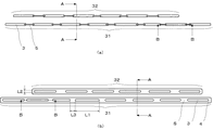
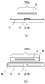
以下、図面に基づき本発明の実施形態を詳述する。図1は、配線基板の一部分を示す上面図である。図1(a)は、電子部品配置面(表面)の上面図であり、図1(b)は裏面の上面図である。図2は、図1のWの拡大図である。図2(a)は、表面のWの拡大図であり、図2(b)は裏面のWの拡大図である。図3は、配線基板のA−A断面図である。図4は、配線基板のB−B断面図である。配線基板1は、配線パターン2、長孔3、半田付部4、ジャンパ線5(金属線)、スルーホール6、半田レジスト7及び複数の電子部品(図示しない)を備えている。
Hereinafter, embodiments of the present invention will be described in detail with reference to the drawings. FIG. 1 is a top view showing a part of a wiring board. FIG. 1A is a top view of the electronic component placement surface (front surface), and FIG. 1B is a top view of the back surface. FIG. 2 is an enlarged view of W in FIG. 2A is an enlarged view of W on the front surface, and FIG. 2B is an enlarged view of W on the back surface. FIG. 3 is a cross-sectional view of the wiring board taken along the line AA. FIG. 4 is a cross-sectional view of the wiring board taken along the line BB. The wiring board 1 includes a wiring pattern 2, a
配線基板1には、配線パターン2が設けられており、配線パターン2には、電子部品等の足が半田付けされるスルーホール6が形成されている。また、この配線パターン2は、配線基板1の部品配置面(表面)と裏面とに対称に設けられており、銅など電気を通しやすく半田付きの良い材料が利用される。 A wiring pattern 2 is provided on the wiring substrate 1, and a through hole 6 in which a foot of an electronic component or the like is soldered is formed in the wiring pattern 2. In addition, the wiring pattern 2 is provided symmetrically on the component placement surface (front surface) and the back surface of the wiring substrate 1, and a material such as copper that easily conducts electricity and has good soldering is used.
スルーホール6に電子部品等(例えば、コンデンサ、抵抗、端子台、リアクトル、スイッチ素子等)の足を表面から挿入して、半田付けによりこれらの電子部品等と配線パターン2とを接続する。これにより、配線基板1は、予め決められた電気回路を構成する。逆に言うと、この配線パターン2は任意の電気回路が構成されるように、配線基板1に設けられることになる。 Legs of electronic components (for example, capacitors, resistors, terminal blocks, reactors, switching elements, etc.) are inserted into the through holes 6 from the surface, and these electronic components and the wiring pattern 2 are connected by soldering. Thereby, the wiring board 1 constitutes a predetermined electric circuit. In other words, the wiring pattern 2 is provided on the wiring board 1 so as to constitute an arbitrary electric circuit.
また、スルーホール6aとスルーホール6bには、別の電子部品が配置され、これらの電子部品間には配線パターン2に沿ってスルーホール6間を電流が流れることになる。尚、図1において配線パターン11は後述する半田レジスト7により隠れることになるため点線で記している。また、スルーホール6の内壁は、配線パターン2と同様の素材(例えば銅や銅合金など)により覆われている。 In addition, another electronic component is arranged in the through hole 6a and the through hole 6b, and a current flows between the through holes 6 along the wiring pattern 2 between these electronic components. In FIG. 1, the wiring pattern 11 is indicated by a dotted line because it is hidden by a solder resist 7 described later. Further, the inner wall of the through hole 6 is covered with the same material as the wiring pattern 2 (for example, copper or copper alloy).
配線パターン11には、電流の流れる方向に沿って(配線パターン11に沿って)複数の長孔3が形成されている。また、この配線パターンには長孔が2列状に配置されており、第1の長孔列31と第2の長孔列32とを構成している。第2の長孔列32の長孔3は、第1の長孔列31の連続する長孔3どうしの間Bに相対向して設けられている。長孔3の内壁は、配線パターン2と同様の素材により覆われ、表面の配線パターンと裏面の配線パターンとを接続している。
A plurality of
また、連続する長孔どうしの間隔をL3とし、長孔3の長手方向の長さをL1とした場合に、間隔L3を長さL1のよりも短くしている。即ち、第1の長孔列31を成す連続する長孔どうしの間隔は第2の長孔列32を成す長孔の長さよりも短くしており、第2の長孔列32を成す長孔の間隔は第1の長孔列31を成す長孔の長さよりも短くしている。
Further, when the interval between the continuous long holes is L3 and the length in the longitudinal direction of the
配線基板1の表面と裏面は、配線パターン2が絶縁素材の半田レジスト7により覆われており、表面側は長孔3の周縁部も含めて半田レジストにより覆われている。また、裏面側の長孔3の周縁部は、半田付けにより半田が付くように周縁部を残して半田レジスト7により覆われ、この長孔3の周縁部の配線パターン2により半田付部4を成している。ここでは、配線パターン11を利用して半田付部4を設けたが、他の導電部材を長孔3に設けて半田付部4としても良い。
The wiring pattern 2 is covered with a solder resist 7 made of an insulating material on the front surface and the back surface of the wiring board 1, and the front surface side is covered with the solder resist including the peripheral portion of the
第1の長孔列31の長孔(一部の長孔)は、同一の半田付部内に設けられて第1の長孔列31を成している。また、第2の長孔列32の長孔(他の長孔)は、第1の長孔列の半田付部と異なる同一の半田付部内に設けられて第2の長孔列を成している。
The long holes (a part of the long holes) of the first
配線基板1には、2つの長孔3間をまたぐジャンパ線5が配置されている。具体的には、第1の長孔列31の隣り合う長孔間をまたぐジャンパ線5が配置される。また、第2の長孔列も同様に、第2の長孔列の隣り合う長孔間をまたぐジャンパ線5が配置される。尚、第1の長孔列31の長孔と該長孔と隣り合う第2の長孔列32の長孔との間をまたぐジャンパ線5を配置しても良い。
On the wiring board 1, a
配線基板1へ電子部品やジャンパ線5等の配置がなされた後半田付けが行われる。半田付けは、鉛フリー半田が用いられ、約220℃〜270℃程度の半田槽に配線基盤1の裏側をつけて行う。この半田付けにより、第1の長孔列31の長孔、及び第2の長孔列32の長孔に半田8が充填されて長孔3が塞がれる(図3、4参照)。また、この半田付けにより、半田付部4に半田8が付着して固まり、半田付部4が半田により覆われる。また、この際に、ジャンパ線5の長孔3へ挿入されている部分が半田に埋まり固定される。
After the electronic parts and the
半田付の際に、長孔3の大きさが小さすぎる場合、長孔3に充填されるはずの半田8が充填されず、長孔3を半田8により塞ぐことができなくなる。また、この際に、長孔3の大きさが大きすぎる場合、長孔3に充填されるはずの半田8が自重により落ちてしまい、長孔3を半田8により塞ぐことができなくなる。
If the size of the
長孔3に十分に半田8を充填して塞ぐために、本実施形態では、長孔3の短手方向の長さL2を1.2mm〜2.5mm程度にし、長孔3の長手方向の長さを、10mm〜30mm程度にしている。
In this embodiment, the length L2 in the short direction of the
以上のように、本実施形態によれば、配線パターン2に、電流の流れる方向に沿って長い長孔3を複数設けて半田により長孔3を塞ぐ。これにより、長孔3を複数に分割することができるので1つ1つの長孔3の大きさを抑えることができ、長孔3を半田8で塞ぎやすくなる。また、第2の長孔列32の長孔は、第1の長孔列31同士の部分に相対向して設けられるため、発熱しやすい個所(長孔と長孔との間)どうしが向かい合うことが無くなるため熱源が分散されて発熱を抑制することができる。
As described above, according to the present embodiment, a plurality of long
また、本実施形態によれば、複数の電子部品が配置される部品配置面側の長孔3の周縁部は半田レジスト7により覆われているため、半田8が長孔から溢れても表面の半田レジスト7に阻まれて表面には半田8が付着しづらくなっている。これにより表面に配置される電子部品と配線パターンとの間に半田8が入って誤導通してしまう事態を抑制することができる。
Further, according to the present embodiment, since the peripheral portion of the
また、裏面の長孔3の周縁部には、半田付けにより半田8が付くように半田付部4が設けられている。このため、溶融半田が冷えて固まる際に、自重により半田が裏面の半田付部に流れ込むとともに半田8が冷やされて体積が小さくなり、長孔3に充填された半田8の配線基板1の表面側が0.3mm〜0.5mmほど凹む(図3の符号C参照)。配線基板1表面に半田8が盛り上がっていると半田8と電子部品とが誤導通してしまう可能性があるが、この凹みCにより電子部品と半田8とが誤導通してしまう事態を抑制することができる。
Further, a
また、長孔3に充填された半田8の配線基板1の裏面側もまた、半田8が冷やされて体積が小さくなることにより0.1mm〜0.2mmほど凹む(図3の符号D参照)。このサイズの凹みC、Dは、長孔3に半田8が満たされた場合に凹む量であり、電流の流れる流路の断面積が大きく取れた証拠であり発熱の抑制効果が十分に得られていると言える。逆に言うと、凹みCが0.3mm〜0.5mmになるように、また、凹みDが、0.1mm〜0.2mmになるように長孔3のサイズを決定すると良い。本実施形態では、長孔3の短手方向の長さL2を1.2mm〜2.5mm程度にし、長孔3の長手方向の長さを、10mm〜30mmにしていることにより、凹みCが0.3mm〜0.5mmになるように、凹みDが、0.1mm〜0.2mmになるようにしている。
Further, the back side of the wiring board 1 of the solder 8 filled in the
また、半田付部4が半田8により覆われることにより、覆われた半田の分だけ、電流の流れる流路の断面積が増えるためより発熱を抑制することができる。
Moreover, since the
また、本実施形態によれば、第1の長孔列31の長孔は、同一の前記半田付部内に設けられて第1の長孔列を成している。このため、第1の長孔列31の長孔間も半田により覆われるので、この分電流の流れる流路の断面積が増え、より発熱を抑制することができる。
Moreover, according to this embodiment, the long hole of the 1st long hole row | line |
また、本実施形態によれば、第2の長孔列32の長孔は、第1の長孔列31の半田付部4と異なる同一の半田付部内4に設けられて第2の長孔列32を成している。このため、第2の長孔列32の長孔間も半田により覆われるので、この分電流の流れる流路の断面積が増え、より発熱を抑制することができる。
Further, according to the present embodiment, the long holes of the second
また、本実施形態によれば、第1の長孔列31を成す長孔の間隔は第2の長孔列32を成す長孔の長さよりも短くしており、第2の長孔列32を成す長孔の間隔は第1の長孔列31を成す長孔の長さよりも短くしている。これにより、第1の長孔列の複数の長孔の間と第2の長孔列32の複数の長孔との間とが向かい合う可能性が小さくなり、熱源が分散されて発熱を抑制することができる。
Further, according to the present embodiment, the interval between the long holes forming the first
また、2つの前記長孔間をまたぐジャンパ線が配置されているため、2つの長孔3間の電流の流れる流路の断面積が増え発熱を抑制することができる。
Moreover, since the jumper wire which straddles between the two said long holes is arrange | positioned, the cross-sectional area of the flow path through which the electric current flows between the two
また、本実施形態によれば、配線パターンが表面、裏面にあり電流路を形成しているので、電流の流れる流路の断面積が増え発熱を抑制することができる。 In addition, according to the present embodiment, since the wiring pattern is on the front surface and the back surface to form a current path, the cross-sectional area of the flow path through which the current flows is increased and heat generation can be suppressed.
以上、本発明の一実施形態について説明したが、以上の説明は本発明の理解を容易にするためのものであり、本発明を限定するものではない。本発明はその趣旨を逸脱することなく、変更、改良され得ると共に本発明にはその等価物が含まれることは勿論である。 As mentioned above, although one Embodiment of this invention was described, the above description is for making an understanding of this invention easy, and does not limit this invention. It goes without saying that the present invention can be changed and improved without departing from the gist thereof, and that the present invention includes equivalents thereof.
例えば、本実施形態で用いたジャンパ線を貫通していない長溝に変えてもよいものである。 For example, the jumper wire used in this embodiment may be changed to a long groove that does not penetrate.
また、例えば、本実施形態では、複数の長孔3により第2の長孔列32を形成していたが、長孔3を1つで第2の長孔列32を形成しても良い。図5に図1のXの拡大図をしめす。図5(a)は、表面のXの拡大図であり、図5(b)は裏面のXの拡大図である。この図では、上述のように第2の長孔列32を長孔3の1つで形成している。
For example, in the present embodiment, the second
また、例えば、本実施形態では、第1の長孔列31及び第2の長孔列32は直線であったが、電流の流れる流路(或いは、配線パターン2)に沿っていれば良い。図6に図1のYの拡大図をしめす。図6(a)は、表面のYの拡大図であり、図6(b)は裏面のYの拡大図である。この図では、上述のように第2の長孔列32bを電流の流れる流路に沿って曲げて配置している。
Further, for example, in the present embodiment, the first
また、例えば、本実施形態では、第1の長孔列31、或いは第2の長孔列32の連続する2つの長孔間をまたぐジャンパ線5を配置していたが、発熱の抑制効果が十分に得られるのであれば必ずしも配置する必要はない。図7に図1のZの拡大図をしめす。図7(a)は、表面のZの拡大図であり、図7(b)は裏面のZの拡大図である。この図では、上述のようにジャンパ線5を配置していない。
In addition, for example, in the present embodiment, the
また、例えば、本実施形態では、長孔3の短手方向の長さL2を1.2mm(下限値)〜2.5mm(上限値)程度にし、長孔3の長手方向の長さを、10mm(下限値)〜30mm(上限値)程度にしていたが、下限値は、半田付けにより半田8が長孔3に充填される大きさがあればよく、上限値は、半田付の際に半田8が自重により落ちて孔があかない大きさであれば良い。この点を満足するには、長孔3の短手方向の長さL2を0.7mm〜3.5mm程度に、長孔3の長手方向の長さを、5mm〜40mm程度にまでできる。
For example, in this embodiment, the length L2 in the short direction of the
1 配線基板
2 配線パターン
3 長孔
4 半田付部
5 ジャンパ線(金属線)
6 スルーホール
7 半田レジスト
8 半田
31 第1の長孔列
32 第2の長孔列
DESCRIPTION OF SYMBOLS 1 Wiring board 2
6 Through-hole 7 Solder resist 8
Claims (7)
設けられ、半田付けにより前記複数の電子部品を前記配線パターンに半田接続している配
線基板において、
前記配線パターンに、前記電流の流れに沿って複数の長孔を設け、前記複数の長孔で前
記電流の流れる方向に沿って第1の長孔列と前記第1の長孔列と並んで設けられる第2の
長孔列とを成し、前記半田により、前記第1の長孔列の長孔、及び前記第2の長孔列の長
孔が塞がれ、
前記第2の長孔列の長孔は、前記第1の長孔列の連続する長孔どうしの間に相対向して設
けられていることを特徴とする配線基板。 In a wiring board in which a plurality of electronic components are arranged, a wiring pattern for flowing a current between the plurality of electronic components is provided, and the plurality of electronic components are soldered to the wiring pattern by soldering.
A plurality of long holes are provided in the wiring pattern along the current flow, and the first long hole row and the first long hole row are aligned along the current flow direction in the plurality of long holes. A second long hole row provided, and the solder closes the long hole of the first long hole row and the long hole of the second long hole row,
The long holes of the second long hole row are provided opposite to each other between the continuous long holes of the first long hole row.
A wiring board characterized by being cut .
より覆われ、裏面の前記長孔の周縁部には、半田が付く半田付部が設けられていることを
特徴とする請求項1に記載の配線基板。 The plurality of electronic components are arranged on the front surface, the peripheral portion of the long hole on the front surface is covered with a solder resist, and the peripheral portion of the long hole on the back surface is provided with a soldering portion for attaching solder. The wiring board according to claim 1.
ことを特徴とする請求項2に記載の配線基板。 Said long hole of the first long hole row, the wiring board according to claim 2, characterized in that said same provided soldering portions constituting the first long hole row.
内に設けられて前記第2の長孔列を成すことを特徴とする請求項2又は請求項3に記載の
配線基板。 The long hole of the second long hole row is provided in the same soldering portion that is different from the soldering portion of the first long hole row to form the second long hole row. Claim | item 2 or the wiring board of Claim 3 .
項1乃至請求項4の何れかに記載の配線基板。 The wiring board according to any one of claims 1 to 4 , wherein a jumper wire straddling between the two continuous long holes is disposed.
し、前記第2の長孔列を成す長孔の間隔は、前記第1の長孔列を成す長孔の長さよりも短
くしていることを特徴とする請求項1乃至請求項5の何れかに記載の配線基板。 The interval between the long holes forming the first long hole row is made shorter than the length of the long hole forming the second long hole row, and the interval between the long holes forming the second long hole row is wiring board according to any one of claims 1 to 5, characterized in that it is shorter than the length of the elongated hole forming the first long hole row.
10〜30mmであることを特徴とする請求項1に記載の配線基板。 2. The wiring board according to claim 1, wherein a length of the long hole in a short direction is 1.2 to 2.5 mm, and a length of the long hole in a longitudinal direction is 10 to 30 mm.
Applications Claiming Priority (1)
| Application Number | Priority Date | Filing Date | Title |
|---|---|---|---|
| PCT/JP2012/065449 WO2013190604A1 (en) | 2012-06-18 | 2012-06-18 | Circuit substrate |
Publications (2)
| Publication Number | Publication Date |
|---|---|
| JPWO2013190604A1 JPWO2013190604A1 (en) | 2016-02-08 |
| JP5909660B2 true JP5909660B2 (en) | 2016-04-27 |
Family
ID=49768236
Family Applications (1)
| Application Number | Title | Priority Date | Filing Date |
|---|---|---|---|
| JP2013546502A Expired - Fee Related JP5909660B2 (en) | 2012-06-18 | 2012-06-18 | Wiring board |
Country Status (4)
| Country | Link |
|---|---|
| EP (1) | EP2699065A4 (en) |
| JP (1) | JP5909660B2 (en) |
| CN (1) | CN204014248U (en) |
| WO (1) | WO2013190604A1 (en) |
Families Citing this family (12)
| Publication number | Priority date | Publication date | Assignee | Title |
|---|---|---|---|---|
| US8900307B2 (en) | 2007-06-26 | 2014-12-02 | DePuy Synthes Products, LLC | Highly lordosed fusion cage |
| US8979860B2 (en) | 2010-06-24 | 2015-03-17 | DePuy Synthes Products. LLC | Enhanced cage insertion device |
| US9592063B2 (en) | 2010-06-24 | 2017-03-14 | DePuy Synthes Products, Inc. | Universal trial for lateral cages |
| US9402732B2 (en) | 2010-10-11 | 2016-08-02 | DePuy Synthes Products, Inc. | Expandable interspinous process spacer implant |
| US9522070B2 (en) | 2013-03-07 | 2016-12-20 | Interventional Spine, Inc. | Intervertebral implant |
| CN109688981A (en) | 2016-06-28 | 2019-04-26 | Eit 新兴移植技术股份有限公司 | Distensible, adjustable angle intervertebral cage |
| CN109688980B (en) | 2016-06-28 | 2022-06-10 | Eit 新兴移植技术股份有限公司 | Expandable and angularly adjustable intervertebral cage with articulation joint |
| US10940016B2 (en) | 2017-07-05 | 2021-03-09 | Medos International Sarl | Expandable intervertebral fusion cage |
| US11446156B2 (en) | 2018-10-25 | 2022-09-20 | Medos International Sarl | Expandable intervertebral implant, inserter instrument, and related methods |
| US11426286B2 (en) | 2020-03-06 | 2022-08-30 | Eit Emerging Implant Technologies Gmbh | Expandable intervertebral implant |
| US11850160B2 (en) | 2021-03-26 | 2023-12-26 | Medos International Sarl | Expandable lordotic intervertebral fusion cage |
| US11752009B2 (en) | 2021-04-06 | 2023-09-12 | Medos International Sarl | Expandable intervertebral fusion cage |
Family Cites Families (8)
| Publication number | Priority date | Publication date | Assignee | Title |
|---|---|---|---|---|
| JPH085576Y2 (en) * | 1991-03-04 | 1996-02-14 | 信越ポリマー株式会社 | Flexible wiring board |
| JPH0747897Y2 (en) | 1992-12-02 | 1995-11-01 | 小島プレス工業株式会社 | Printed board |
| JPH06204628A (en) * | 1992-12-10 | 1994-07-22 | Hitachi Aic Inc | Printed wiring board |
| JPH09107162A (en) * | 1995-10-13 | 1997-04-22 | Murata Mfg Co Ltd | Printed circuit board |
| JPH09153664A (en) * | 1995-11-30 | 1997-06-10 | Toshiba Corp | Substrate for large current |
| WO2009121697A1 (en) * | 2008-04-01 | 2009-10-08 | Continental Automotive Gmbh | Current-carrying component comprising a carrier, conductor tracks and conductor laminae |
| JP2009277863A (en) * | 2008-05-14 | 2009-11-26 | Toyota Industries Corp | Method of manufacturing wiring substrate |
| JP2010165808A (en) * | 2009-01-15 | 2010-07-29 | Mitsubishi Electric Corp | Electronic control device |
-
2012
- 2012-06-18 WO PCT/JP2012/065449 patent/WO2013190604A1/en active Application Filing
- 2012-06-18 EP EP12866412.5A patent/EP2699065A4/en not_active Withdrawn
- 2012-06-18 JP JP2013546502A patent/JP5909660B2/en not_active Expired - Fee Related
- 2012-06-18 CN CN201290000940.5U patent/CN204014248U/en not_active Expired - Fee Related
Also Published As
| Publication number | Publication date |
|---|---|
| EP2699065A4 (en) | 2014-08-13 |
| WO2013190604A1 (en) | 2013-12-27 |
| JPWO2013190604A1 (en) | 2016-02-08 |
| CN204014248U (en) | 2014-12-10 |
| EP2699065A1 (en) | 2014-02-19 |
Similar Documents
| Publication | Publication Date | Title |
|---|---|---|
| JP5909660B2 (en) | Wiring board | |
| JP5224067B2 (en) | Board terminal and board connector having the same | |
| JP2011159923A (en) | Electronic device | |
| JP2017038017A (en) | Noise reducing substrate and electronic equipment | |
| JP4650948B2 (en) | Through-hole soldering structure | |
| JP2009182141A (en) | Electronic apparatus and method of manufacturing the same | |
| JP2015065197A (en) | Jumper element or resistance element for current detection | |
| JP5213074B2 (en) | Printed wiring board and pad design method used therefor | |
| JP2015177039A (en) | Printed board and printed board with terminal using the same | |
| JP6114044B2 (en) | Printed board | |
| JP5836863B2 (en) | Surface mount module, terminal of surface mount module, method of manufacturing terminal of surface mount module, and surface mount module mounting board | |
| JP2016092138A5 (en) | ||
| JP2016025228A (en) | Circuit structure | |
| JP2016225395A (en) | Printed circuit board and electronic device | |
| US9374897B2 (en) | Printed wiring board | |
| JP2015211109A (en) | Electronic circuit board | |
| JP6345554B2 (en) | Printed wiring board | |
| JP6521681B2 (en) | Side-mounted light emitting device | |
| JP2018129464A (en) | Printed circuit board and printed circuit device | |
| JP4803071B2 (en) | Circuit board and circuit board with electronic components | |
| JP2016082026A (en) | Printed circuit board | |
| JP2009060006A (en) | Soldering pallet | |
| JP6727115B2 (en) | Wiring board for electronic control unit | |
| JP2020004772A (en) | Printed circuit board with jumper portion | |
| JP2014183147A (en) | Printed wiring board |
Legal Events
| Date | Code | Title | Description |
|---|---|---|---|
| TRDD | Decision of grant or rejection written | ||
| A01 | Written decision to grant a patent or to grant a registration (utility model) |
Free format text: JAPANESE INTERMEDIATE CODE: A01 Effective date: 20160105 |
|
| A61 | First payment of annual fees (during grant procedure) |
Free format text: JAPANESE INTERMEDIATE CODE: A61 Effective date: 20160118 |
|
| R151 | Written notification of patent or utility model registration |
Ref document number: 5909660 Country of ref document: JP Free format text: JAPANESE INTERMEDIATE CODE: R151 |
|
| LAPS | Cancellation because of no payment of annual fees |