JP5907899B2 - Spatial light modulator backplane device and method for operating the backplane device - Google Patents
Spatial light modulator backplane device and method for operating the backplane device Download PDFInfo
- Publication number
- JP5907899B2 JP5907899B2 JP2012557532A JP2012557532A JP5907899B2 JP 5907899 B2 JP5907899 B2 JP 5907899B2 JP 2012557532 A JP2012557532 A JP 2012557532A JP 2012557532 A JP2012557532 A JP 2012557532A JP 5907899 B2 JP5907899 B2 JP 5907899B2
- Authority
- JP
- Japan
- Prior art keywords
- pixel
- tft
- line
- addressing
- backplane device
- Prior art date
- Legal status (The legal status is an assumption and is not a legal conclusion. Google has not performed a legal analysis and makes no representation as to the accuracy of the status listed.)
- Active
Links
- 238000000034 method Methods 0.000 title claims description 39
- 238000012546 transfer Methods 0.000 claims description 22
- 230000007423 decrease Effects 0.000 claims description 10
- 230000009977 dual effect Effects 0.000 claims description 6
- 230000003213 activating effect Effects 0.000 claims description 5
- 238000004380 ashing Methods 0.000 claims 1
- 230000005540 biological transmission Effects 0.000 description 68
- 230000006870 function Effects 0.000 description 55
- 238000010586 diagram Methods 0.000 description 42
- 239000004973 liquid crystal related substance Substances 0.000 description 34
- 238000013461 design Methods 0.000 description 11
- 239000011159 matrix material Substances 0.000 description 11
- 210000004027 cell Anatomy 0.000 description 10
- 230000008901 benefit Effects 0.000 description 9
- 239000003990 capacitor Substances 0.000 description 9
- 238000013459 approach Methods 0.000 description 7
- 239000000758 substrate Substances 0.000 description 7
- 230000009365 direct transmission Effects 0.000 description 5
- 238000004064 recycling Methods 0.000 description 5
- 230000008859 change Effects 0.000 description 4
- 230000001276 controlling effect Effects 0.000 description 4
- 230000000694 effects Effects 0.000 description 4
- 239000011521 glass Substances 0.000 description 4
- 230000002441 reversible effect Effects 0.000 description 4
- 229910021417 amorphous silicon Inorganic materials 0.000 description 3
- 238000009826 distribution Methods 0.000 description 3
- 238000005516 engineering process Methods 0.000 description 3
- 229910021421 monocrystalline silicon Inorganic materials 0.000 description 3
- 229910021420 polycrystalline silicon Inorganic materials 0.000 description 3
- 229920005591 polysilicon Polymers 0.000 description 3
- 230000002829 reductive effect Effects 0.000 description 3
- 230000004044 response Effects 0.000 description 3
- 230000000630 rising effect Effects 0.000 description 3
- 230000003068 static effect Effects 0.000 description 3
- XUIMIQQOPSSXEZ-UHFFFAOYSA-N Silicon Chemical compound [Si] XUIMIQQOPSSXEZ-UHFFFAOYSA-N 0.000 description 2
- 230000003044 adaptive effect Effects 0.000 description 2
- 239000004020 conductor Substances 0.000 description 2
- 230000003247 decreasing effect Effects 0.000 description 2
- 230000005684 electric field Effects 0.000 description 2
- 239000000463 material Substances 0.000 description 2
- 230000004048 modification Effects 0.000 description 2
- 238000012986 modification Methods 0.000 description 2
- 229910052710 silicon Inorganic materials 0.000 description 2
- 239000010703 silicon Substances 0.000 description 2
- 238000003860 storage Methods 0.000 description 2
- 239000010409 thin film Substances 0.000 description 2
- 230000004913 activation Effects 0.000 description 1
- 230000001174 ascending effect Effects 0.000 description 1
- 230000004397 blinking Effects 0.000 description 1
- 230000000903 blocking effect Effects 0.000 description 1
- 230000001427 coherent effect Effects 0.000 description 1
- 238000012937 correction Methods 0.000 description 1
- 230000009849 deactivation Effects 0.000 description 1
- 238000011161 development Methods 0.000 description 1
- 230000018109 developmental process Effects 0.000 description 1
- 238000005868 electrolysis reaction Methods 0.000 description 1
- 230000004907 flux Effects 0.000 description 1
- 230000008571 general function Effects 0.000 description 1
- AMGQUBHHOARCQH-UHFFFAOYSA-N indium;oxotin Chemical compound [In].[Sn]=O AMGQUBHHOARCQH-UHFFFAOYSA-N 0.000 description 1
- 230000010354 integration Effects 0.000 description 1
- 230000000670 limiting effect Effects 0.000 description 1
- 238000004519 manufacturing process Methods 0.000 description 1
- 239000002052 molecular layer Substances 0.000 description 1
- 230000003287 optical effect Effects 0.000 description 1
- 238000007254 oxidation reaction Methods 0.000 description 1
- 230000000737 periodic effect Effects 0.000 description 1
- 230000001105 regulatory effect Effects 0.000 description 1
- 239000004065 semiconductor Substances 0.000 description 1
- 238000000926 separation method Methods 0.000 description 1
- 238000004088 simulation Methods 0.000 description 1
- 210000000352 storage cell Anatomy 0.000 description 1
- 238000012360 testing method Methods 0.000 description 1
- 230000001960 triggered effect Effects 0.000 description 1
Images


Classifications
-
- G—PHYSICS
- G09—EDUCATION; CRYPTOGRAPHY; DISPLAY; ADVERTISING; SEALS
- G09G—ARRANGEMENTS OR CIRCUITS FOR CONTROL OF INDICATING DEVICES USING STATIC MEANS TO PRESENT VARIABLE INFORMATION
- G09G3/00—Control arrangements or circuits, of interest only in connection with visual indicators other than cathode-ray tubes
- G09G3/20—Control arrangements or circuits, of interest only in connection with visual indicators other than cathode-ray tubes for presentation of an assembly of a number of characters, e.g. a page, by composing the assembly by combination of individual elements arranged in a matrix no fixed position being assigned to or needed to be assigned to the individual characters or partial characters
-
- G—PHYSICS
- G02—OPTICS
- G02B—OPTICAL ELEMENTS, SYSTEMS OR APPARATUS
- G02B30/00—Optical systems or apparatus for producing three-dimensional [3D] effects, e.g. stereoscopic images
-
- G—PHYSICS
- G03—PHOTOGRAPHY; CINEMATOGRAPHY; ANALOGOUS TECHNIQUES USING WAVES OTHER THAN OPTICAL WAVES; ELECTROGRAPHY; HOLOGRAPHY
- G03H—HOLOGRAPHIC PROCESSES OR APPARATUS
- G03H1/00—Holographic processes or apparatus using light, infrared or ultraviolet waves for obtaining holograms or for obtaining an image from them; Details peculiar thereto
- G03H1/02—Details of features involved during the holographic process; Replication of holograms without interference recording
-
- G—PHYSICS
- G03—PHOTOGRAPHY; CINEMATOGRAPHY; ANALOGOUS TECHNIQUES USING WAVES OTHER THAN OPTICAL WAVES; ELECTROGRAPHY; HOLOGRAPHY
- G03H—HOLOGRAPHIC PROCESSES OR APPARATUS
- G03H1/00—Holographic processes or apparatus using light, infrared or ultraviolet waves for obtaining holograms or for obtaining an image from them; Details peculiar thereto
- G03H1/22—Processes or apparatus for obtaining an optical image from holograms
- G03H1/2294—Addressing the hologram to an active spatial light modulator
-
- G—PHYSICS
- G09—EDUCATION; CRYPTOGRAPHY; DISPLAY; ADVERTISING; SEALS
- G09G—ARRANGEMENTS OR CIRCUITS FOR CONTROL OF INDICATING DEVICES USING STATIC MEANS TO PRESENT VARIABLE INFORMATION
- G09G3/00—Control arrangements or circuits, of interest only in connection with visual indicators other than cathode-ray tubes
- G09G3/20—Control arrangements or circuits, of interest only in connection with visual indicators other than cathode-ray tubes for presentation of an assembly of a number of characters, e.g. a page, by composing the assembly by combination of individual elements arranged in a matrix no fixed position being assigned to or needed to be assigned to the individual characters or partial characters
- G09G3/2085—Special arrangements for addressing the individual elements of the matrix, other than by driving respective rows and columns in combination
-
- G—PHYSICS
- G03—PHOTOGRAPHY; CINEMATOGRAPHY; ANALOGOUS TECHNIQUES USING WAVES OTHER THAN OPTICAL WAVES; ELECTROGRAPHY; HOLOGRAPHY
- G03H—HOLOGRAPHIC PROCESSES OR APPARATUS
- G03H1/00—Holographic processes or apparatus using light, infrared or ultraviolet waves for obtaining holograms or for obtaining an image from them; Details peculiar thereto
- G03H1/22—Processes or apparatus for obtaining an optical image from holograms
-
- G—PHYSICS
- G03—PHOTOGRAPHY; CINEMATOGRAPHY; ANALOGOUS TECHNIQUES USING WAVES OTHER THAN OPTICAL WAVES; ELECTROGRAPHY; HOLOGRAPHY
- G03H—HOLOGRAPHIC PROCESSES OR APPARATUS
- G03H1/00—Holographic processes or apparatus using light, infrared or ultraviolet waves for obtaining holograms or for obtaining an image from them; Details peculiar thereto
- G03H1/02—Details of features involved during the holographic process; Replication of holograms without interference recording
- G03H2001/0208—Individual components other than the hologram
- G03H2001/0224—Active addressable light modulator, i.e. Spatial Light Modulator [SLM]
-
- G—PHYSICS
- G03—PHOTOGRAPHY; CINEMATOGRAPHY; ANALOGOUS TECHNIQUES USING WAVES OTHER THAN OPTICAL WAVES; ELECTROGRAPHY; HOLOGRAPHY
- G03H—HOLOGRAPHIC PROCESSES OR APPARATUS
- G03H2225/00—Active addressable light modulator
- G03H2225/20—Nature, e.g. e-beam addressed
- G03H2225/22—Electrically addressed SLM [EA-SLM]
-
- G—PHYSICS
- G09—EDUCATION; CRYPTOGRAPHY; DISPLAY; ADVERTISING; SEALS
- G09G—ARRANGEMENTS OR CIRCUITS FOR CONTROL OF INDICATING DEVICES USING STATIC MEANS TO PRESENT VARIABLE INFORMATION
- G09G2310/00—Command of the display device
- G09G2310/02—Addressing, scanning or driving the display screen or processing steps related thereto
- G09G2310/0243—Details of the generation of driving signals
- G09G2310/0259—Details of the generation of driving signals with use of an analog or digital ramp generator in the column driver or in the pixel circuit
-
- G—PHYSICS
- G09—EDUCATION; CRYPTOGRAPHY; DISPLAY; ADVERTISING; SEALS
- G09G—ARRANGEMENTS OR CIRCUITS FOR CONTROL OF INDICATING DEVICES USING STATIC MEANS TO PRESENT VARIABLE INFORMATION
- G09G2320/00—Control of display operating conditions
- G09G2320/02—Improving the quality of display appearance
- G09G2320/0223—Compensation for problems related to R-C delay and attenuation in electrodes of matrix panels, e.g. in gate electrodes or on-substrate video signal electrodes
Landscapes
- Physics & Mathematics (AREA)
- Engineering & Computer Science (AREA)
- General Physics & Mathematics (AREA)
- Computer Hardware Design (AREA)
- Theoretical Computer Science (AREA)
- Optics & Photonics (AREA)
- Control Of Indicators Other Than Cathode Ray Tubes (AREA)
- Liquid Crystal (AREA)
- Liquid Crystal Display Device Control (AREA)
- Devices For Indicating Variable Information By Combining Individual Elements (AREA)
- Holo Graphy (AREA)
Description
本発明は、空間光変調器のバックプレーンデバイス及びバックプレーンデバイスを操作する方法に関する。 The present invention relates to a spatial light modulator backplane device and a method for operating the backplane device.
空間光変調器は、特に、情報を表示するために使用される高解像度ディスプレイの形態の表示装置において使用されるように設計される。本発明の適用分野は、画素を非常に迅速に制御する必要のある場合にその目的で使用される高解像度ディスプレイ、特に、TFT(薄膜トランジスタ)ディスプレイ及びLCOS(Liquid Crystal On Silicon)を含む。別の適用分野は、空間光変調器を含む光学素子である。かかる素子は、光束の方向又は形状、或いは、コヒーレント波面の形状に影響を及ぼす。 Spatial light modulators are specifically designed to be used in display devices in the form of high-resolution displays used to display information. Fields of application of the present invention include high resolution displays used for that purpose when the pixels need to be controlled very quickly, in particular TFT (Thin Film Transistor) displays and LCOS (Liquid Crystal On Silicon). Another field of application is optical elements including spatial light modulators. Such elements affect the direction or shape of the light flux or the shape of the coherent wavefront.
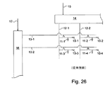
図26は、4つの画素電極11−1、11−2、11−3及び11−4を含む従来技術におけるバックプレーンデバイスのアクティブマトリクス(AM)構造の一例を示す。ゲート線は、ディスプレイ全体の画素を書き込むように順に起動される。しかしながら、益々向上する解像度及びリフレッシュレートが、例えば、ホログラムディスプレイにおけるホログラムの表現に必要であるため、従来の表示装置において使用されるような全体的な行線及び列線を使用するこの種のアドレッシングは、それら解像度及びリフレッシュレートに関して不十分であることが分かる。 FIG. 26 shows an example of an active matrix (AM) structure of a backplane device in the prior art including four pixel electrodes 11-1, 11-2, 11-3, and 11-4. The gate lines are activated in sequence to write the pixels of the entire display. However, this kind of addressing using overall row and column lines as used in conventional display devices, for example, because increasingly improved resolutions and refresh rates are necessary, for example, for the representation of holograms in holographic displays. Are inadequate with respect to their resolution and refresh rate.
例えば、図28に示すように、列線上で周波数を上げることは、データ線全体が各クロックサイクル中にデータ線の抵抗及び容量に対して再充電されなければならないことを意味する。これにより、高い出力駆動電流及び高い電力損が発生する。また、線の高いインピーダンスは、この線に接続された全てのTFTのゲート容量により更に増加する。 For example, as shown in FIG. 28, increasing the frequency on the column line means that the entire data line must be recharged to the resistance and capacitance of the data line during each clock cycle. As a result, high output drive current and high power loss occur. Also, the high impedance of the line is further increased by the gate capacitance of all TFTs connected to this line.
列線の容量及び全ての画素TFTのゲートは、非常に短い間隔で電荷反転を受けなければならない。その結果、周波数が上がるため電力損失が増加する。コンダクタのインピーダンス及び容量による規定限度があり、それを超えると、1つのクロックサイクルでコンダクタにおいて完全な電荷反転を実現するのは不可能である。 The column line capacitance and the gates of all pixel TFTs must undergo charge reversal at very short intervals. As a result, the power loss increases because the frequency increases. There are defined limits due to the impedance and capacitance of the conductor, beyond which it is impossible to achieve full charge reversal in the conductor in one clock cycle.
その結果、ほぼ全ての今日のLCD(液晶ディスプレイ)バックプレーンデバイスにおいて使用されるアクティブマトリクス構造は、例えば、1000Hz以上の範囲において高速フレームレートで高解像度ディスプレイ(例えば、16000画素×8000画素)を駆動できない。そのようなディスプレイは、例えば、参考として本明細書に取り入れられる国際公開第2006/066919号パンフレットにおいて開示されるように、特に、ホログラムディスプレイの適用例に対して必要である。そのような高フレームレートが必要な理由は、特に、仮想観察者ウィンドウ(VOW)が1人以上の観察者に対して時系列に生成されなければならないためである。 As a result, active matrix structures used in almost all today's LCD (liquid crystal display) backplane devices drive high resolution displays (eg, 16000 pixels x 8000 pixels) at high frame rates, for example, in the range of 1000 Hz and higher. Can not. Such a display is particularly necessary for holographic display applications, for example as disclosed in WO 2006/066919, which is incorporated herein by reference. The reason why such a high frame rate is required is especially because a virtual observer window (VOW) must be generated in time series for one or more observers.
また、線の高いインピーダンスは、全ての接続されたTFTゲート容量により更に増加する。両方の特徴を組み合わせることにより、最大データ線周波数を制限する。その結果、高フレームレートの高解像度ディスプレイに対して、従来のアクティブマトリクス設計を使用することは実現不可能であると考えられる。 Also, the high impedance of the line is further increased by all connected TFT gate capacitances. Combining both features limits the maximum data line frequency. As a result, it seems impossible to use a conventional active matrix design for high frame rate, high resolution displays.
国際公開第2009/092717号パンフレットは、ディスプレイを小クラスタにタイルのように配列することでAMの問題のうちのいくつかを克服し、且つ、アナログシフトレジスタを使用してこれらのクラスタを外部から独立して駆動する方法を開示する。ディスプレイをクラスタにタイルのように配列し、且つ、非常に少ないが高速の外側のドライバからクラスタ回路へのポイントツーポイント接続を使用することにより、非常に高い解像度及び非常に高速なディスプレイが可能になる。しかしながら、全てのこれらの種類のディスプレイは、表示位置によりソートされた線単位で画素値を画素に割り当てる。画素値が線毎に変化する場合、これは、高周波数で再充電されるシフトレジスタの高電圧のアナログデータ線又はその部分を必要とする。 WO 2009/092717 overcomes some of the problems of AM by arranging the displays in small clusters like tiles, and uses analog shift registers to remove these clusters from the outside. A method of independently driving is disclosed. Arranging displays like tiles in clusters and using very few but fast outer drivers to point to point connections to the cluster circuit allows very high resolution and very fast displays Become. However, all these types of displays assign pixel values to pixels in line units sorted by display position. If the pixel value changes from line to line, this requires a high voltage analog data line or part of the shift register that is recharged at a high frequency.
これは、通常、空間光変調器にわたり一様に分布した画素値を含むホログラムディスプレイに対して特に不都合である。従って、これらの従来技術の種類のディスプレイを用いる場合、一般にホログラムディスプレイは、一般的なLCディスプレイと同一の電力損を有する。最悪の場合、チェスボードテストパターンの画素値が画素に割り当てられる。 This is particularly disadvantageous for hologram displays that typically contain pixel values that are uniformly distributed across the spatial light modulator. Thus, when using these prior art types of displays, holographic displays generally have the same power loss as typical LC displays. In the worst case, the pixel values of the chess board test pattern are assigned to the pixels.
LTPS(低温ポリシリコン)の不均一性がアナログシフトレジスタに対して必要なアナログ回路の実現例を複雑にするため、例えば、国際公開第2009/024523号パンフレット又は国際公開第2009/092717号パンフレットにおいて開示されたような画素クラスタ及びアナログシフトレジスタを使用して特別に開発されたバックプレーン構造は、今日のLTPS TFTを用いて実現することは困難である。 Non-uniformity of LTPS (low temperature polysilicon) complicates the implementation of an analog circuit that is necessary for an analog shift register. For example, in WO2009 / 024523 or WO2009 / 092717 Backplane structures specially developed using pixel clusters and analog shift registers as disclosed are difficult to implement using today's LTPS TFTs.
従って、本発明の目的は、非常に高速に又は高フレームレートで、例えば、300Hz以上、特に、300Hz〜1800Hz又はそれ以上で動作する空間光変調器、特に、高解像度ディスプレイのバックプレーンデバイスを提供することである。 Accordingly, it is an object of the present invention to provide a spatial light modulator, particularly a high-resolution display backplane device, operating at very high speeds or at high frame rates, eg, 300 Hz or higher, especially 300 Hz to 1800 Hz or higher. It is to be.
上述の問題は、空間光変調器のバックプレーンデバイスによる請求項1の特徴により規定された本発明により解決される。そのような空間光変調器は、特に、シーン又はコンテンツの2次元表現及び/又は3次元表現を生成する表示装置において適用される。空間光変調器は、画素アドレスを有し、且つ、画素値を画素に割り当てるようにバックプレーンデバイスにより電子制御可能な画素を含む。バックプレーンデバイスは、画素毎に少なくとも1つの電極と、少なくとも1つのアナログ線と、少なくとも1つの画素アドレッシング手段とを含む。そのような画素アドレッシング手段は、xアドレッシング線及びyアドレッシング線を含む。全ての画素は、アナログ線、xアドレッシング線及びyアドレッシング線に接続される。画素値割当方式として、生成手段が少なくとも1つのアドレス線に適用される電圧特性を生成するように構成され、電圧特性は画素に割り当てられる画素値に依存する。バックプレーンデバイスは、画素アドレスが画素アドレッシング方式として生成された電圧特性に依存して決定されるように構成される。バックプレーンデバイスは、生成された電圧特性が画素値を画素に割り当てるために少なくとも1つのアナログ線に適用されるように更に構成される。
The above problem is solved by the present invention as defined by the features of
バックプレーンデバイスの単一の画素が、その後、行単位で、且つ、アドレス指定された行内で同時に又は画素単位でアドレス指定されるアクティブマトリクスバックプレーンなどの従来技術のバックプレーンデバイスの画素アドレッシング方式に従うのではなく、本発明は全く異なる画素アドレッシング方式を使用する。データ線又はアナログ線の容量及びデータ線に接続された全ての画素のトランジスタゲート容量は、全てクロックサイクル毎にデータ線抵抗を介して再充電されなければならない。これにより、高い出力駆動電流及び高い電力損が発生する。また、データ線の高いインピーダンスは、接続された全てのTFTのゲート容量により更に増加する。双方の特徴を組み合わせることにより、最大データ線周波数を制限する。その結果、360Hz以上のフレームレートで駆動された24インチを超える高解像度ディスプレイに対して、従来のアクティブマトリクス設計を使用することは実現不可能であると考えられる。 A single pixel of a backplane device is then subject to a pixel addressing scheme of a prior art backplane device such as an active matrix backplane that is addressed row-by-row and simultaneously within the addressed row or pixel-by-pixel. Instead, the present invention uses a completely different pixel addressing scheme. The capacity of the data line or analog line and the transistor gate capacity of all pixels connected to the data line must all be recharged via the data line resistance every clock cycle. As a result, high output drive current and high power loss occur. Further, the high impedance of the data line is further increased by the gate capacitance of all the connected TFTs. Combining both features limits the maximum data line frequency. As a result, it would not be feasible to use conventional active matrix designs for high resolution displays greater than 24 inches driven at a frame rate of 360 Hz or higher.
本発明に係る画素アドレッシング方式は、画素に割り当てられる画素値に依存している。従って、本発明の画素アドレッシング方式は、画素に割り当てられる画素値に依存して、例えば、1つの画素において最小電圧の画素値及び次の画素において最大電圧が2つのクロックサイクル内で割り当てられなければならない従来技術のシステムにおいて使用されている一般的なアナログ線上で非常に高い周波数を有することを防止する。本発明は、より低い周波数を含むアナログ線に適用されている電圧特性又は電圧機能を得ることを試みている。これは、例えば、電圧特性であるランプアップ関数をアナログ線に適用することで実現される。次に、単一の画素は、アナログ線に適用されている電圧特性、特に、アナログ線に適用されている実際の電圧値に依存してアドレス指定される。換言すれば、特定の画素は、この特定の画素に割り当てられる画素値に対応する電圧特性の電圧値がアナログ線上に適用される時にアドレス指定されている。従って、アナログ線に適用されている高周波数電圧特性は、(少なくとも画素クロック範囲に対して)阻止され、やや平滑な又はより低い周波数電圧特性がアナログ線に適用される。そのようにするために、アナログ線に適用されている電圧特性に依存して画素をアドレス指定する必要がある。この結果、高周波数信号がxアドレッシング線及びyアドレッシング線に適用される可能性が最も高い。しかしながら、これは、より高い電圧が印加されるアナログ線回路ではなく、同一の(低)電圧のデジタル信号が適用されるデジタルアドレッシング回路に関する。 The pixel addressing scheme according to the present invention depends on the pixel value assigned to the pixel. Accordingly, the pixel addressing scheme of the present invention depends on the pixel value assigned to the pixel, for example, if the pixel value of the minimum voltage in one pixel and the maximum voltage in the next pixel are not assigned within two clock cycles. Preventing having a very high frequency on a typical analog line used in prior art systems that should not. The present invention attempts to obtain a voltage characteristic or voltage function that is applied to analog lines containing lower frequencies. This is realized, for example, by applying a ramp-up function that is a voltage characteristic to an analog line. A single pixel is then addressed depending on the voltage characteristics applied to the analog line, in particular the actual voltage value applied to the analog line. In other words, a particular pixel is addressed when a voltage value with a voltage characteristic corresponding to the pixel value assigned to this particular pixel is applied on the analog line. Thus, the high frequency voltage characteristics applied to the analog lines are blocked (at least for the pixel clock range) and a somewhat smoother or lower frequency voltage characteristic is applied to the analog lines. To do so, it is necessary to address the pixels depending on the voltage characteristics applied to the analog lines. As a result, a high frequency signal is most likely applied to the x addressing line and the y addressing line. However, this relates to a digital addressing circuit to which the same (low) voltage digital signal is applied, not an analog line circuit to which a higher voltage is applied.
従来技術のアドレッシング方式に従って、最新のディスプレイの低速デジタル信号はトランジスタゲートの小容量を充電し、高周波数アナログ信号は大容量の画素電極を駆動する。本発明は、本発明の画素回路のアドレッシング方式を用いて、高周波数信号を画素回路の小ゲート容量に適用し、且つ、相対的に低速なアナログ信号を大容量の画素電極に適用することでこれを交換する。換言すれば、従来技術のアドレッシング方式に従ってアドレス線上に転送される大電荷又はより大きい電荷ではなく、小電荷は、本発明のアドレッシング方式を用いてアドレッシング線上に高周波数で転送される。 In accordance with prior art addressing schemes, low-speed digital signals in modern displays charge a small capacity of the transistor gate and high-frequency analog signals drive a large capacity pixel electrode. The present invention uses the pixel circuit addressing method of the present invention to apply a high-frequency signal to a small gate capacitance of the pixel circuit and to apply a relatively low-speed analog signal to a large-capacity pixel electrode. Replace this. In other words, small charges, rather than large or larger charges transferred on the address lines according to the prior art addressing scheme, are transferred at a high frequency on the addressing lines using the addressing scheme of the present invention.
高解像度ディスプレイの場合、高い画素開口率を有するためにより小さなトランジスタ及び線構造サイズを有することが有用である。これにより、考えられる駆動電流が減少する。これに反して、最新のディスプレイは、線の数が増加するにもかかわらず、フレームレートを維持するためにより高速な伝送時間を実現するより大きな電流を必要とする。トランジスタ構造サイズを減少することにより、トランジスタゲート容量及び閾値電圧も減少する。より小さなゲート容量により、より高いトランジスタスイッチング周波数、より低い電圧レベル及びより小さい電流が可能になるため、本発明はより小さな構造サイズから利益を得る。より低い電圧及びより小さい電流により、最新の実現例と比較して電力損が減少する。 For high resolution displays, it is useful to have smaller transistors and line structure sizes to have a high pixel aperture ratio. This reduces the possible drive current. On the other hand, modern displays require more current to achieve faster transmission times to maintain the frame rate, despite the increased number of lines. By reducing the transistor structure size, the transistor gate capacitance and threshold voltage are also reduced. The present invention benefits from a smaller structure size because a smaller gate capacitance allows for higher transistor switching frequency, lower voltage level and smaller current. The lower voltage and smaller current reduces the power loss compared to the current implementation.
好適な実施形態において、バックプレーンデバイス又は空間光変調器は、バックプレーンデバイスの画素電極に対する対向電極を含む。アナログ線は、接地に接続される。本発明に係る画素アドレッシング方式が適用されると同時に、アナログ線ではなく、対向電極は生成された電圧特性と共に適用される。通常、接地接続又は接地線は、一般に、例えば、画素電極に接続されたアドレス復号器回路又は記憶コンデンサに対して、いずれにしてもバックプレーンデバイス上で必要とされる。液晶層は、2つのガラス基板により取り囲まれる。一方のガラス基板は、TFTを有し、且つ、TFT上に書き込むバックプレーンデバイスを備える。他方のガラス基板は、殆どの例において、ガラス基板上の平坦な導電性の透明なITO(インジウムスズ酸化物)層である共通電極(対向電極とも呼ぶ)を含む。画素電極は、一方のコンタクト又は画素コンデンサの一部である。共通電極は、他方のコンタクト又は全ての画素コンデンサの一部を形成する。本実施形態に従って生成された電圧特性が共通電極上に適用される場合、これは、バックプレーンデバイスの全ての画素の画素電極に影響を及ぼす。以下に説明するように、バックプレーンデバイスがクラスタを含む場合、これは同様に全てのクラスタに影響を及ぼす。クラスタが画素値の種々の分布を有する場合、遅延サイクルは、アドレッシング方式に追加されなければならず、全てのクラスタに対して同一のランプ関数を使用できなければならない。しかしながら、ホログラムディスプレイが規則的にほぼ一様に分布した画素値を含むため、非常に少ない遅延サイクルを追加する必要がある。 In a preferred embodiment, the backplane device or spatial light modulator includes a counter electrode to the pixel electrode of the backplane device. The analog line is connected to ground. At the same time as the pixel addressing method according to the present invention is applied, not the analog line but the counter electrode is applied with the generated voltage characteristics. Usually, a ground connection or ground line is generally required on the backplane device anyway, for example for an address decoder circuit or storage capacitor connected to the pixel electrode. The liquid crystal layer is surrounded by two glass substrates. One glass substrate has a TFT and a backplane device for writing on the TFT. The other glass substrate includes, in most examples, a common electrode (also referred to as a counter electrode) which is a flat conductive transparent ITO (indium tin oxide) layer on the glass substrate. The pixel electrode is part of one contact or pixel capacitor. The common electrode forms the other contact or part of all pixel capacitors. When the voltage characteristics generated according to this embodiment are applied on the common electrode, this affects the pixel electrodes of all the pixels of the backplane device. As explained below, if the backplane device contains clusters, this also affects all clusters. If the clusters have different distributions of pixel values, the delay cycle must be added to the addressing scheme and the same ramp function must be available for all clusters. However, since the holographic display contains regularly and substantially uniformly distributed pixel values, very few delay cycles need to be added.
電力損を更に減少するために、非常に効率的な電荷再利用が可能である。高周波数デジタル信号は、非常に小さなゲート容量のみを駆動する。古い画素電圧と新しい画素電圧との差が評価される場合、アドレス指定された画素を巧妙にソートすることは、外部駆動なしで1つの画素から別の画素に電荷を転送するため、或いは、アナログ線の値を上昇又は低下させるために使用される。転送が独立した時間毎に起動及び停止される場合、電荷再利用は更により効率的である。例えば、これは、付録の2.1節に示される。 In order to further reduce power loss, very efficient charge recycling is possible. High frequency digital signals only drive very small gate capacitances. If the difference between the old pixel voltage and the new pixel voltage is evaluated, clever sorting of addressed pixels can be used to transfer charge from one pixel to another without external drive, or analog Used to increase or decrease the line value. Charge transfer is even more efficient if transfers are started and stopped at independent times. For example, this is shown in section 2.1 of the appendix.
イネーブル動作及びディスエーブル動作を用いた駆動方式により、フレーム時間の大部分に対して、アナログ線を介して画素容量を充電するように時間を設定できる。これにより、相対的に長い伝送時間を使用して高画素容量を充電するために小電流を使用できる。アナログ線上の低周波数のため、アナログ信号は、伝送トランジスタが切り替えられ、且つ、画素値を画素に格納する瞬間に既に着実に選択された画素の伝送トランジスタのソース上に適用される。これにより、画素電極上で電圧を更により正確に制御できるため、より高いグレースケール解像度(ビット深度)、特に、高画素周波数が得られる。 With the driving method using the enable operation and the disable operation, the time can be set so that the pixel capacitance is charged via the analog line for most of the frame time. This allows a small current to be used to charge a high pixel capacity using a relatively long transmission time. Due to the low frequency on the analog line, the analog signal is applied on the source of the transmission transistor of the pixel already steadily selected at the moment the transmission transistor is switched and the pixel value is stored in the pixel. This allows the voltage to be controlled more accurately on the pixel electrode, resulting in a higher gray scale resolution (bit depth), particularly a high pixel frequency.
一般に、提案された本発明は、主に、より小さな構造サイズから利益を得る一方で、最新の解決方法は性能を犠牲にする。 In general, the proposed invention benefits primarily from smaller structure sizes, while modern solutions sacrifice performance.
本発明に従って値をソートする手法は、クロックサイクル毎に1つ又は非常に少ない画素にのみアクセスできる。従って、マトリクスに対する画素数は、必要なフレーム時間及び1つの画素に対して実現可能なアクセス時間により制限される。1つ又は非常に少ない画素のみが同時にアドレス指定されるため、1つのクラスタに対する画素数は制限される。しかしながら、統合されたアドレス復号器を用いる場合、外部からクラスタへの接続の数は非常に少なく、それにより、多くの数の高速であるが低解像度のクラスタを高速で高解像度のディスプレイにすることができる。 The method of sorting values according to the present invention can access only one or very few pixels per clock cycle. Thus, the number of pixels for the matrix is limited by the required frame time and the access time that can be achieved for one pixel. Since only one or very few pixels are addressed simultaneously, the number of pixels for one cluster is limited. However, when using an integrated address decoder, the number of external connections to the cluster is very small, thereby making many high-speed but low-resolution clusters faster and higher-resolution displays. Can do.
他の従来技術の表示装置は、例えば、デジタル−アナログ変換器として画素を使用するためにアナログランプ線、並びに、xアドレス線及びyアドレス線を含む図7において説明された3TFT画素回路に類似した画素回路を使用する。しかしながら、本発明と異なり、画素は、フレーム毎ではなく、線毎に1つの固定パターンのランプアップサイクル/ランプダウンサイクルで線毎にアドレス指定される。 Other prior art display devices are similar to the 3 TFT pixel circuit described in FIG. 7 including, for example, analog ramp lines and x address lines and y address lines to use the pixels as digital-to-analog converters. A pixel circuit is used. However, unlike the present invention, the pixels are addressed line by line in a fixed pattern ramp-up / ramp-down cycle per line, not per frame.
電荷が単一の画素に転送される画素のアドレスが現在アナログ線に適用されている電圧値によりソートされるように、画素の値は、この画素がアドレス指定される場合に少なくとも1つのアナログ線上に適用されている実際の電圧値を示すかそれに対応する。
「電圧特性」という用語の本明細書における意味は、ある特定の期間の一定値を含むが、ある特定の期間の更に可変である電圧機能として理解される。
The value of the pixel is on at least one analog line when this pixel is addressed, so that the address of the pixel whose charge is transferred to a single pixel is sorted by the voltage value currently applied to the analog line. Shows or corresponds to the actual voltage value applied to.
The meaning of the term “voltage characteristic” herein is understood as a voltage function that includes a constant value for a certain period, but is more variable for a certain period.
本発明に対して「画素値を画素に割り当てる」という用語は、特に、電圧が画素の電極に印加される結果、殆どの場合、電荷が画素の電極に転送すること又は画素の電極から転送することであると理解される。そのような画素値により、空間光変調器は、本発明に従ってバックプレーンにより操作される空間光変調器の種類に依存して輝度値又は色値などを示す。 For the purposes of the present invention, the term “assigning a pixel value to a pixel” particularly means that, in most cases, charge is transferred to or from the pixel electrode as a result of a voltage being applied to the pixel electrode. It is understood that. With such pixel values, the spatial light modulator exhibits a luminance value, a color value, etc. depending on the type of spatial light modulator operated by the backplane according to the present invention.
電圧特性は、電圧ランプアップ関数又は電圧ランプダウン関数である。双方の組合せが適用されることが好ましい。すなわち、電圧ランプダウン関数に後続して電圧ランプアップ関数が適用されることが好ましい。或いは、更に、のこぎり歯関数が適用される。そのようなのこぎり歯関数は、急峻な立上り端及び急峻な立下り端が後続する緩やかに減少する特性又は緩やかに増加する特性、或いは、緩やかに減少する特性が後続する緩やかに増加する特性を含む。電圧特性は、所定の期間、オーバドライブ値を含むことが好ましい。或いは、更に、電圧特性は、所定の期間、アンダドライブ値を含むことが好ましい。そのようなオーバドライブ値又はアンダドライブ値は、特に該当する場合は常に上述の他の電圧特性と組み合わせて適用される。 The voltage characteristic is a voltage ramp-up function or a voltage ramp-down function. It is preferred that a combination of both be applied. That is, it is preferable that the voltage ramp-up function is applied subsequent to the voltage ramp-down function. Alternatively, in addition, a sawtooth function is applied. Such sawtooth functions include a slowly decreasing characteristic or a slowly increasing characteristic followed by a steep rising edge and a steep falling edge, or a slowly increasing characteristic followed by a slowly decreasing characteristic. . The voltage characteristic preferably includes an overdrive value for a predetermined period. Alternatively, the voltage characteristic preferably includes an underdrive value for a predetermined period. Such overdrive values or underdrive values are applied in combination with the other voltage characteristics described above, wherever applicable.
通常、電圧特性は、時間において可変であり、主に、数学的な単調関数又は級数の特性を有する。これは、電圧特性が単一の急峻な立上り端又は立下り端を含まないことを意味しない。しかしながら、単一の急峻な立上り端又は立下り端が発生した後、後続の電圧特性は、通常、主に、数学的な単調関数又は級数の特性を有する。特に、電圧特性は、単調増加又は単調減少している。 Usually, the voltage characteristic is variable in time and mainly has a mathematical monotonic function or series characteristic. This does not mean that the voltage characteristic does not include a single steep rising or falling edge. However, after the occurrence of a single steep rising or falling edge, the subsequent voltage characteristic usually has mainly a mathematical monotonic function or series characteristic. In particular, the voltage characteristic monotonously increases or monotonously decreases.
本発明の特に好適な実施形態において、少なくとも1つのアナログ線に適用されている生成された電圧特性は、画素のアドレッシングの順序を決定する。例えば、少なくとも1つのアナログ線に適用されている生成された電圧特性が低電圧値から開始し、且つ、高電圧値に増加するランプアップ関数を含む場合、低電圧値が適用される必要のある画素(この画素に割り当てられる画素値が低電圧値に対応するため)は、最初にアドレス指定される。ランプアップ関数の電圧値が別の電圧値に増加し、この他の電圧値が1つ以上の画素に割り当てられる次に増加した画素値を示す場合、この次の電圧値が1つの画素又はこれらのより多くの画素に割り当てられるように、この1つの画素又はこれらのより多くの画素はアドレス指定される。同一の電圧値が複数の画素に適用される場合には画素をアドレス指定する特定の順序はないが、本発明の実施形態に従って、種々の電圧値、即ち、画素に割り当てられる画素値に対する画素のアドレッシングの順序がある。 In a particularly preferred embodiment of the invention, the generated voltage characteristic applied to at least one analog line determines the order of pixel addressing. For example, if the generated voltage characteristic applied to at least one analog line includes a ramp-up function starting from a low voltage value and increasing to a high voltage value, the low voltage value needs to be applied The pixel (because the pixel value assigned to this pixel corresponds to a low voltage value) is addressed first. If the voltage value of the ramp-up function increases to another voltage value and this other voltage value indicates the next increased pixel value assigned to one or more pixels, then this next voltage value is one pixel or these This one pixel or these more pixels are addressed so that they are assigned to more pixels. There is no specific order of addressing pixels when the same voltage value is applied to multiple pixels, but according to embodiments of the present invention, various voltage values, i.e., the pixel values for the pixel values assigned to the pixels. There is an order of addressing.
本発明の好適な実施形態において、決定されている画素アドレスは、x方向及びy方向に対して生成される。画素値を画素に割り当てることは、x方向及びy方向に対して、ランダムアクセス方式で実行される。これは、電圧特性が画素に割り当てられる画素値に依存して決定されないために、生成されたsin関数などの周期関数、或いは、直線の線形増加/減少特性を含むランプアップ関数及び/又はランプダウン関数である場合に特に当てはまる。従って、定義上、その後、バックプレーンの各行がアドレス指定されるという従来技術のような画素をアドレス指定する特定の順序は存在しない。これが特定の状況において本発明のアドレッシング方式に従う場合であっても、例えば、画素の隣接する行が僅かに増加する画素値に割り当てられるべきであり、且つ、行内において画素値が一定である場合、一般にこれは当てはまらない。従来技術のアドレッシング方式と異なり、アドレッシング方式、即ち、本発明の本実施形態に従って画素値を画素に割り当てることは、ランダムアクセス方式で実行される。従って、画素をランダムアクセス方式でアドレス指定するため、適用される固定の行サイクル又はフレームサイクルは存在しない。 In the preferred embodiment of the present invention, the determined pixel addresses are generated for the x and y directions. Assigning pixel values to pixels is performed in a random access manner in the x and y directions. This is because the voltage characteristic is not determined depending on the pixel value assigned to the pixel, so the generated function is a periodic function such as a sin function, or a ramp-up function and / or a ramp-down that includes a linear linear increase / decrease characteristic. This is especially true for functions. Thus, by definition, there is no specific order for addressing pixels as in the prior art, where each row of the backplane is then addressed. Even if this is the case when following the addressing scheme of the present invention in certain circumstances, for example, if adjacent rows of pixels should be assigned to slightly increasing pixel values and the pixel values are constant within a row, In general this is not the case. Unlike the prior art addressing scheme, the addressing scheme, ie assigning pixel values to pixels according to this embodiment of the present invention, is performed in a random access scheme. Thus, there is no fixed row or frame cycle applied to address the pixels in a random access manner.
同一の画素値が割り当てられる全ての画素は、バックプレーンデバイスの1つの動作モードで互いに時間的に近接してアドレス指定されることが好ましい。上述したように、これは、電圧特性がランプアップ関数及び/又はランプダウン関数を含む場合に特に適用される。バックプレーンデバイスの別の好適な動作モードにおいて、同一の画素値が割り当てられる全ての画素は、実質的に同時にアドレス指定される。多くの画素又は全ての画素を同一の画素値に割り当てなければならない場合、或いは、多くの画素又は全ての画素の画素値を所定の画素値に再設定しなければならない場合、バックプレーンデバイスのそのような動作モードが適用される。バックプレーンデバイスの更に別の動作モードにおいて、同一の画素値が割り当てられる全ての画素は、ある期間アドレス指定される。画素値が一度に1つの画素だけに割り当てられる場合、バックプレーンデバイスのこの動作モードが特に適用される。その後、5つの画素を同一の画素値に割り当てる必要がある場合、画素値が一度に1つの画素だけに割り当てられるため、この動作には、ある期間である5画素書込みサイクルが必要となる。 All pixels that are assigned the same pixel value are preferably addressed in close proximity to each other in one mode of operation of the backplane device. As mentioned above, this applies especially when the voltage characteristic includes a ramp-up function and / or a ramp-down function. In another preferred mode of operation of the backplane device, all pixels that are assigned the same pixel value are addressed substantially simultaneously. If many or all pixels have to be assigned to the same pixel value, or if many or all pixels have to be reset to a given pixel value, that of the backplane device Such an operation mode is applied. In yet another mode of operation of the backplane device, all pixels that are assigned the same pixel value are addressed for a period of time. This mode of operation of the backplane device is particularly applicable when pixel values are assigned to only one pixel at a time. Thereafter, if it is necessary to assign five pixels to the same pixel value, the pixel value is assigned to only one pixel at a time, so this operation requires a period of five pixel writing cycles.
バックプレーンの特定の動作モードにおいて、画素値が一度に1つの画素だけに割り当てられる。この動作モードにおいて、全ての画素は、順次、次々に割り当てられる。 In a particular mode of operation of the backplane, pixel values are assigned to only one pixel at a time. In this mode of operation, all pixels are assigned sequentially one after the other.
本発明の好適な実施形態において、空間光変調器及び/又はバックプレーンデバイスは、画素の少なくとも2つのクラスタのクラスタ配列を含む。各クラスタは、アナログ線及びクラスタの画素をアドレス指定する画素アドレッシング手段を含む。各クラスタのアナログ線は、例えば、バックプレーンデバイスのドライバ手段の外部電圧源とクラスタ自体との間に接続される。クラスタは、互いに個別に制御されることが好ましい。従って、特定のクラスタに対する画素値は、この特定のクラスタのアドレッシング手段及びアナログ線により、この特定のクラスタの画素に割り当てられ、別のクラスタに対する画素値は、同時に又は時間をずらして個別にこの他のクラスタのアドレッシング手段及びアナログ線により、この他のクラスタの画素に割り当てられる。種々の適用例に対して適切なクラスタの例は、正方形形状であり、64×64画素、128×128画素、256×256画素又は1024×1024画素を含む。「クラスタ」という用語の本発明における意味は、特に、複数の画素が配列されることにより、空間光変調器の接続領域又は隣接領域を形成することを意味する。そのような領域は、矩形形状、正方形形状又はハニカム形状を有する。クラスタは、空間光変調器の全幅又は全長に及ばないことが好ましい。x方向又はy方向のクラスタの画素数は2nである必要はなく、nは自然数である。 In a preferred embodiment of the present invention, the spatial light modulator and / or backplane device includes a cluster arrangement of at least two clusters of pixels. Each cluster includes an analog line and pixel addressing means for addressing the pixels of the cluster. The analog line of each cluster is connected, for example, between the external voltage source of the driver means of the backplane device and the cluster itself. The clusters are preferably controlled individually from each other. Accordingly, the pixel values for a particular cluster are assigned to the pixels of this particular cluster by the addressing means and analog lines of this particular cluster, and the pixel values for another cluster can be individually or otherwise shifted separately. The other cluster addressing means and analog lines are assigned to the other cluster pixels. Examples of suitable clusters for various applications are square shapes and include 64 × 64 pixels, 128 × 128 pixels, 256 × 256 pixels, or 1024 × 1024 pixels. The meaning of the term “cluster” in the present invention particularly means that a connection region or an adjacent region of the spatial light modulator is formed by arranging a plurality of pixels. Such a region has a rectangular shape, a square shape or a honeycomb shape. The clusters preferably do not extend over the full width or length of the spatial light modulator. The number of pixels in the cluster in the x direction or the y direction need not be 2 n , and n is a natural number.
一般に、能動的に制御可能なスイッチング素子を含む全ての種類の基板は、本発明に係るバックプレーンデバイスを実現するために使用される。一例は、単結晶シリコンから構成された基板を含むLCOS(Liquid Crystal On Silicon)ディスプレイである。他の可能性は、LTPS、a−Si、アモルファス酸化物TFT又は有機TFTなどから構成されたTFTを含む基板である。 In general, all types of substrates including actively controllable switching elements are used to implement the backplane device according to the present invention. One example is a Liquid Crystal On Silicon (LCOS) display that includes a substrate composed of single crystal silicon. Another possibility is a substrate comprising a TFT composed of LTPS, a-Si, amorphous oxide TFT or organic TFT.
TFT及びトランジスタという用語は、明細書及び特許請求の範囲において同義であり、全てのトランジスタがTFTから構成され、全てのTFTが単結晶シリコン又は他の半導体材料などから構成された他の種類のトランジスタ、或いは、他の能動的なスイッチング素子により置換されることを意味する。 The terms TFT and transistor are synonymous in the specification and claims, and all types of transistors are composed of TFTs, and all TFTs are composed of monocrystalline silicon or other semiconductor materials. Alternatively, it is meant to be replaced by another active switching element.
以下において、バックプレーンデバイスの画素の制御回路を実行する種々の可能性を説明する。なお、通常、空間光変調器又はバックプレーンデバイスの全ての画素は同一の制御回路を含むが、空間光変調器又はバックプレーンデバイスにおいて適用されている画素に対して異なる制御回路を有することができてもよい。 In the following, various possibilities for implementing the pixel control circuit of the backplane device will be described. Normally, all pixels of a spatial light modulator or backplane device include the same control circuit, but can have different control circuits for pixels applied in the spatial light modulator or backplane device. May be.
第1の実施形態において、画素に対する制御回路は、2つのTFTを含む。第1のTFTは、アナログ線、xアドレッシング線及び第2のTFTに接続される。第2のTFTは、第1のTFT、yアドレッシング線及び画素の電極に接続される。なお、第1のTFTがxアドレッシング線に接続され、第2のTFTがyアドレッシング線に接続されるが、逆であってもよい。換言すれば、第1のTFTはyアドレッシング線に接続され、第2のTFTはxアドレッシング線に接続される。これは、以下において説明する画素にも当てはまる。xアドレッシング線及びyアドレッシング線に接続されたゲートを含む2つのトランジスタを、デュアルゲートトランジスタに結合することが有利である。第1の実施形態において、デュアルゲートTFTは、選択TFT(この場合、第1のTFT)及び伝送TFT(この場合、第2のTFT)の機能を結合する。 In the first embodiment, the control circuit for the pixel includes two TFTs. The first TFT is connected to the analog line, the x addressing line, and the second TFT. The second TFT is connected to the first TFT, the y addressing line, and the pixel electrode. The first TFT is connected to the x addressing line and the second TFT is connected to the y addressing line, but the reverse may be possible. In other words, the first TFT is connected to the y addressing line, and the second TFT is connected to the x addressing line. This also applies to the pixels described below. It is advantageous to couple two transistors including gates connected to the x addressing line and the y addressing line into a dual gate transistor. In the first embodiment, the dual gate TFT combines the functions of a selection TFT (in this case, a first TFT) and a transmission TFT (in this case, a second TFT).
更なる実施形態において、xアドレッシング線及びyアドレッシング線に接続されたTFTは、伝送TFTのゲート上の電圧を制御することで伝送TFTをon又はoffするかを選択する選択TFTとして機能している。伝送TFTのソースはアナログ線に接続され、伝送TFTのドレインは画素電極に接続される。このトランジスタをonする場合、電荷はアナログ線から画素電極に転送される。伝送トランジスタをoffする場合、現在印加されている電荷が画素電極上に格納されることで画素値を規定する。 In a further embodiment, the TFT connected to the x addressing line and the y addressing line functions as a selection TFT that selects whether the transmission TFT is turned on or off by controlling the voltage on the gate of the transmission TFT. . The source of the transmission TFT is connected to the analog line, and the drain of the transmission TFT is connected to the pixel electrode. When this transistor is turned on, the charge is transferred from the analog line to the pixel electrode. When the transmission transistor is turned off, the pixel value is defined by storing the currently applied charge on the pixel electrode.
第2の実施形態において、画素に対する制御回路は、2つのTFTを含む。第1のTFTは、選択TFTとして機能しており、xアドレッシング線、yアドレッシング線及び第2のTFTに接続される。第2のTFTは、伝送TFTとして機能しており、第1のTFT、アナログ線及び画素の電極に接続される。そのような画素回路は、DRAM(ダイナミックランダムアクセスメモリ)記憶セルの回路に相当する。伝送TFTのゲート容量において格納又は印加された電荷は、伝送TFTをon又はoffするかを決定する。本発明の画素割当方式及び画素アドレッシング方式は、特に、マルチレベルの目的のためにDRAM技術又はFLASH技術に適用される。この場合、画素は記憶セルに対応し、画素電極は記憶セルのコンデンサの電極に対応する。画素値を画素に割り当てることは、情報(ビット又はマルチレベルビット)を記憶セルに格納することに対応する。 In the second embodiment, the control circuit for the pixel includes two TFTs. The first TFT functions as a selection TFT, and is connected to the x addressing line, the y addressing line, and the second TFT. The second TFT functions as a transmission TFT and is connected to the first TFT, the analog line, and the pixel electrode. Such a pixel circuit corresponds to a DRAM (dynamic random access memory) memory cell circuit. The charge stored or applied in the gate capacitance of the transmission TFT determines whether the transmission TFT is turned on or off. The pixel allocation and pixel addressing schemes of the present invention are particularly applicable to DRAM technology or FLASH technology for multi-level purposes. In this case, the pixel corresponds to the memory cell, and the pixel electrode corresponds to the capacitor electrode of the memory cell. Assigning a pixel value to a pixel corresponds to storing information (bits or multilevel bits) in a storage cell.
バックプレーンデバイスは少なくとも1つのイネーブル線を含み、全ての画素はイネーブル線に接続されることが好ましい。これは、以下において説明する画素回路の第3の実施形態から第5の実施形態に当てはまる。 The backplane device preferably includes at least one enable line and all pixels are connected to the enable line. This applies to the third to fifth embodiments of the pixel circuit described below.
第3の実施形態において、画素に対する制御回路は、3つのTFTを含む。第1のTFTは、イネーブル線、xアドレッシング線及び第2のTFTに接続される。第2のTFTは、第1のTFT、yアドレッシング線及び第3のTFTに接続される。第3のTFTは、第2のTFT、アナログ線及び画素の電極に接続される。この回路が種々の方法で操作されるため、この画素回路は、ホログラム表示装置において適用される空間光変調器に対して好まれる。 In the third embodiment, the control circuit for the pixel includes three TFTs. The first TFT is connected to the enable line, the x addressing line, and the second TFT. The second TFT is connected to the first TFT, the y addressing line, and the third TFT. The third TFT is connected to the second TFT, the analog line, and the pixel electrode. Since this circuit is operated in various ways, this pixel circuit is preferred for spatial light modulators applied in hologram display devices.
第4の実施形態において、画素に対する制御回路は、3つのTFTを含む。ここで、2つの画素は、互いに隣接して配置され、同一のyアドレッシング線によりアドレス指定される。第1の画素の第1のTFTは、イネーブリング機能として、第2の画素のxアドレッシング線、yアドレッシング線及び第1の画素の第2のTFTに接続される。第1の画素の第2のTFTは、第1の画素の第1のTFT、第1の画素のxアドレッシング線及び第1の画素の第3のTFTに接続される。第1の画素の第3のTFTは、第1の画素の第2のTFT、アナログ線及び第1の画素の電極に接続される。第2の画素の第1のTFTは、イネーブリング機能として、第1の画素のxアドレッシング線、yアドレッシング線及び第2の画素の第2のTFTに接続される。第2の画素の第2のTFTは、第2の画素の第1のTFT、第2の画素のxアドレッシング線及び第2の画素の第3のTFTに接続される。第2の画素の第3のTFTは、第2の画素の第2のTFT、アナログ線及び第2の画素の電極に接続される。本実施形態は、画素のイネーブルメント機能性に対してバックプレーンデバイス上に独立したイネーブル線を有する必要はない。これは、2つの隣接画素の一方の画素のxアドレッシング線を他方の画素に対するイネーブル線として使用することで実現される。これは、イネーブル線の論理レベルがxアドレッシング線の論理レベルに対応する場合に実行される。 In the fourth embodiment, the control circuit for the pixel includes three TFTs. Here, the two pixels are arranged adjacent to each other and are addressed by the same y addressing line. The first TFT of the first pixel is connected to the x addressing line, the y addressing line of the second pixel, and the second TFT of the first pixel as an enabling function. The second TFT of the first pixel is connected to the first TFT of the first pixel, the x addressing line of the first pixel, and the third TFT of the first pixel. The third TFT of the first pixel is connected to the second TFT of the first pixel, the analog line, and the electrode of the first pixel. The first TFT of the second pixel is connected to the x addressing line, the y addressing line of the first pixel, and the second TFT of the second pixel as an enabling function. The second TFT of the second pixel is connected to the first TFT of the second pixel, the x addressing line of the second pixel, and the third TFT of the second pixel. The third TFT of the second pixel is connected to the second TFT of the second pixel, the analog line, and the electrode of the second pixel. This embodiment need not have an independent enable line on the backplane device for pixel enablement functionality. This is realized by using the x addressing line of one pixel of two adjacent pixels as an enable line for the other pixel. This is performed when the logic level of the enable line corresponds to the logic level of the x addressing line.
第5の実施形態において、画素に対する制御回路は、3つのTFTを含む。4つの画素は、互いに隣接して配置され、同一のyアドレッシング線によりアドレス指定される。第1の画素の第1のTFTは、イネーブリング機能として、第3の画素のxアドレッシング線、yアドレッシング線及び第1の画素の第2のTFTに接続される。第1の画素の第2のTFTは、第1の画素の第1のTFT、第1の画素のxアドレッシング線及び第1の画素の第3のTFTに接続される。第1の画素の第3のTFTは、第1の画素の第2のTFT、アナログ線及び第1の画素の電極に接続される。第2の画素の第1のTFTは、イネーブリング機能として、第1の画素のxアドレッシング線、yアドレッシング線及び第2の画素の第2のTFTに接続される。第2の画素の第2のTFTは、第2の画素の第1のTFT、第2の画素のxアドレッシング線及び第2の画素の第3のTFTに接続される。第2の画素の第3のTFTは、第2の画素の第2のTFT、アナログ線及び第2の画素の電極に接続される。第3の画素の第1のTFTは、イネーブリング機能として、第4の画素のxアドレッシング線、yアドレッシング線及び第3の画素の第2のTFTに接続される。第3の画素の第2のTFTは、第3の画素の第1のTFT、第3の画素のxアドレッシング線及び第3の画素の第3のTFTに接続される。第3の画素の第3のTFTは、第3の画素の第2のTFT、アナログ線及び第3の画素の電極に接続される。第4の画素の第1のTFTは、イネーブリング機能として、第2の画素のxアドレッシング線、yアドレッシング線及び第4の画素の第2のTFTに接続される。第4の画素の第2のTFTは、第4の画素の第1のTFT、第4の画素のxアドレッシング線及び第4の画素の第3のTFTに接続される。第4の画素の第3のTFTは、第4の画素の第2のTFT、アナログ線及び第4の画素の電極に接続される。第4の実施形態と同様に、本実施形態は、画素のイネーブルメント機能性に対してバックプレーンデバイス上に独立したイネーブル線を有する必要はない。これは、1つの画素に対して4つの隣接画素の他の画素のうちの1つのxアドレッシング線がこの画素に対するイネーブル線として使用される場合に実現される。これは、イネーブル線の論理レベルがxアドレッシング線の論理レベルに対応する場合に実行される。 In the fifth embodiment, the control circuit for the pixel includes three TFTs. The four pixels are arranged adjacent to each other and are addressed by the same y addressing line. The first TFT of the first pixel is connected to the x addressing line, the y addressing line of the third pixel, and the second TFT of the first pixel as an enabling function. The second TFT of the first pixel is connected to the first TFT of the first pixel, the x addressing line of the first pixel, and the third TFT of the first pixel. The third TFT of the first pixel is connected to the second TFT of the first pixel, the analog line, and the electrode of the first pixel. The first TFT of the second pixel is connected to the x addressing line, the y addressing line of the first pixel, and the second TFT of the second pixel as an enabling function. The second TFT of the second pixel is connected to the first TFT of the second pixel, the x addressing line of the second pixel, and the third TFT of the second pixel. The third TFT of the second pixel is connected to the second TFT of the second pixel, the analog line, and the electrode of the second pixel. The first TFT of the third pixel is connected to the x addressing line, the y addressing line of the fourth pixel, and the second TFT of the third pixel as an enabling function. The second TFT of the third pixel is connected to the first TFT of the third pixel, the x addressing line of the third pixel, and the third TFT of the third pixel. The third TFT of the third pixel is connected to the second TFT of the third pixel, the analog line, and the electrode of the third pixel. The first TFT of the fourth pixel is connected to the x addressing line, the y addressing line of the second pixel, and the second TFT of the fourth pixel as an enabling function. The second TFT of the fourth pixel is connected to the first TFT of the fourth pixel, the x addressing line of the fourth pixel, and the third TFT of the fourth pixel. The third TFT of the fourth pixel is connected to the second TFT of the fourth pixel, the analog line, and the electrode of the fourth pixel. Similar to the fourth embodiment, this embodiment need not have independent enable lines on the backplane device for pixel enablement functionality. This is realized when one x addressing line of other pixels of the four adjacent pixels is used as one enable line for this pixel. This is performed when the logic level of the enable line corresponds to the logic level of the x addressing line.
上述のTFT要素又はトランジスタ要素が挙げられるが、伝送トランジスタ及び選択トランジスタの機能を能動的に実現する他の回路及び/又は他のスイッチング要素が代わりにバックプレーンデバイスに対して使用又は適用されてよい。 Although the TFT elements or transistor elements mentioned above may be mentioned, other circuits and / or other switching elements that actively implement the functions of the transfer transistor and the selection transistor may be used or applied to the backplane device instead. .
画素の第1のTFT及び同一の画素の第2のTFTがデュアルゲートに結合される結果、画素回路の更なる簡潔性が得られ、空間を節約することが有利である。これは、上述の5つの実施形態に対して実行される。 As a result of the first TFT of the pixel and the second TFT of the same pixel being combined into a dual gate, further simplicity of the pixel circuit is obtained and it is advantageous to save space. This is performed for the five embodiments described above.
原則的に、TFTのゲート、ソース及びドレインの接続のために多くの可能性が存在するが、以下において、上述の5つの実施形態のTFTを接続する最も好適な方法を説明する。これらの接続の方法は、互いに更に組み合わされる。 In principle, there are many possibilities for connecting the gate, source and drain of the TFT, but in the following, the most preferred method of connecting the TFTs of the above five embodiments will be described. These connection methods are further combined with each other.
xアドレッシング線又はyアドレッシング線は、画素の第1のTFTのゲートと接続されるか、或いは、画素の第2のTFTのゲート又は上述のデュアルゲートTFTのゲートに接続される。 The x addressing line or the y addressing line is connected to the gate of the first TFT of the pixel, or is connected to the gate of the second TFT of the pixel or the gate of the dual gate TFT described above.
イネーブル線又はイネーブル線として動作するxアドレッシング線は、画素の第1のTFTのソースと接続される。画素の第1のTFTのドレインは、同一の画素の第2のTFTのソースに接続される。 The enable line or the x addressing line that operates as the enable line is connected to the source of the first TFT of the pixel. The drain of the first TFT of the pixel is connected to the source of the second TFT of the same pixel.
アナログ線は、画素の第3のTFTのソースに接続され、同一の画素の電極は、同一の画素の第3のTFTのドレインと接続される。画素の第2のTFTのドレインは、同一の画素の第3のTFTのゲートに接続される。 The analog line is connected to the source of the third TFT of the pixel, and the electrode of the same pixel is connected to the drain of the third TFT of the same pixel. The drain of the second TFT of the pixel is connected to the gate of the third TFT of the same pixel.
画素アドレッシング手段は、少なくとも1つのxアドレス復号器及び少なくとも1つのyアドレス復号器を備えることが好ましい。xアドレス復号器はxアドレッシング線に接続され、yアドレス復号器はyアドレッシング線に接続される。 The pixel addressing means preferably comprises at least one x address decoder and at least one y address decoder. The x address decoder is connected to the x addressing line, and the y address decoder is connected to the y addressing line.
アドレス復号器は、単一又は全てのアドレッシング線のイネーブルメントを実行する論理回路を含む。xアドレス復号器及び/又はyアドレス復号器は、ダイナミックNOR復号器、及び/又は、ダイナミックNAND復号器、及び/又は、OR復号器、及び/又は、NAND回路及びNOR回路を含むCMOS復号器、及び/又は、AND復号器に基づく。 The address decoder includes logic that performs enablement of a single or all addressing lines. x-address decoder and / or y-address decoder may be a dynamic NOR decoder and / or a dynamic NAND decoder and / or an OR decoder and / or a CMOS decoder including a NAND circuit and a NOR circuit; And / or based on an AND decoder.
空間光変調器の種類及びそれを用いて実現されることを意図する適用例に依存して、xアドレス復号器及び/又はyアドレス復号器は、バックプレーンデバイス上又はバックプレーンデバイスに対する種々の位置において配列される。xアドレス復号器及び/又はyアドレス復号器は、バックプレーンデバイスとは別に配列される。また、xアドレス復号器及び/又はyアドレス復号器は、バックプレーンデバイスの外側エッジにおいて配置される。更に別の方法は、画素間のバックプレーンデバイス上にxアドレス復号器及び/又はyアドレス復号器を配置することである。 Depending on the type of spatial light modulator and the application intended to be realized with it, the x-address decoder and / or the y-address decoder can have different positions on or relative to the backplane device. Arranged in The x address decoder and / or the y address decoder are arranged separately from the backplane device. Also, the x address decoder and / or the y address decoder are located at the outer edge of the backplane device. Yet another method is to place an x address decoder and / or a y address decoder on the backplane device between the pixels.
例えば、バックプレーンデバイス又は1つのクラスタの全ての画素がイネーブル線を含む3つの画素回路等の同一の種類の画素回路を含む場合、画素の画素回路を互いに配向する種々の方法がある。全ての画素制御構造が同様に配向されることを意味する規則的なレイアウトで画素制御構造が配列される画素制御構造を各画素が含むのが好ましい。或いは、2つの隣接画素の画素制御構造は、互いにミラーリングされて配列される。ミラーリングされた配列に対する対称の軸は、2つの画素の中間にある。2つの画素がx方向に互いに隣接する場合、対称の軸はy方向に配向される。更に別の方法は、共通の中心に隣接して配置される4つの隣接画素の画素制御構造が互いにミラーリングされて配列される方法である。対称の第1の軸は、2つの画素間及び共通の中心上に位置付けられ、対称の第2の軸は、2つの画素間及び共通の中心上、及び、対称の第1の軸に対して垂直に位置付けられる。そのようにミラーリングされたレイアウトにより、アナログ線、イネーブル線、或いは、電力又は画素の記憶容量に対して必要な線等の全ての画素に共通の線を提供する労力が減少する。 For example, when all the pixels of a backplane device or one cluster include the same type of pixel circuit, such as three pixel circuits including enable lines, there are various ways to orient the pixel circuits of the pixels relative to each other. Each pixel preferably includes a pixel control structure in which the pixel control structures are arranged in a regular layout meaning that all pixel control structures are similarly oriented. Alternatively, the pixel control structures of two adjacent pixels are arranged in a mirrored manner. The axis of symmetry for the mirrored array is in the middle of the two pixels. If two pixels are adjacent to each other in the x direction, the axis of symmetry is oriented in the y direction. Yet another method is a method in which pixel control structures of four adjacent pixels arranged adjacent to a common center are arranged in a mirrored manner. A first axis of symmetry is located between the two pixels and on the common center, and a second axis of symmetry is between the two pixels and on the common center and with respect to the first axis of symmetry. Positioned vertically. Such a mirrored layout reduces the effort of providing a common line for all pixels, such as analog lines, enable lines, or lines needed for power or pixel storage capacity.
好適な実施形態において、空間光変調器は、回折に基づいて空間光変調器と相互作用する光を偏向するように構成される。ここで、空間光変調器は、国際公開第2010/149587号パンフレットの請求項のうちの1つに従って実現されることが好ましい。そのような空間光変調器は、回折格子構造に対応する屈折率分布が符号化される制御可能な液晶分子層を含む。そのような回折格子/パターンと相互作用する光は、空間光変調器により回折される。空間光変調器は、空間光変調器に符号化される回折格子が可変ピッチを有する回折格子を含むように操作されることが好ましい。従って、空間光変調器と相互作用する光の偏向角は変動する。そのような空間光変調器は、1つの方向に線形に延長され、互いに隣接して配置される電極を含む。従って、そのような空間光変調器の画素は、空間光変調器の延長された線形領域である。そのような空間光変調器の更なる詳細については、参考として本明細書に完全に取り入れられる国際公開第2010/149587号パンフレットを参照する。 In a preferred embodiment, the spatial light modulator is configured to deflect light that interacts with the spatial light modulator based on diffraction. Here, the spatial light modulator is preferably realized according to one of the claims of WO 2010/149487. Such a spatial light modulator includes a controllable liquid crystal molecular layer in which the refractive index profile corresponding to the diffraction grating structure is encoded. Light that interacts with such a diffraction grating / pattern is diffracted by the spatial light modulator. The spatial light modulator is preferably operated such that the diffraction grating encoded in the spatial light modulator includes a diffraction grating having a variable pitch. Therefore, the deflection angle of light interacting with the spatial light modulator varies. Such spatial light modulators include electrodes that extend linearly in one direction and are arranged adjacent to each other. Thus, the pixels of such a spatial light modulator are an extended linear region of the spatial light modulator. For further details of such a spatial light modulator, reference is made to WO 2010/149487, which is fully incorporated herein by reference.
上述の問題は、空間光変調器のバックプレーンデバイスを操作する方法による請求項25の特徴により規定された本発明により解決される。空間光変調器は、画素アドレスを有し、且つ、画素値を画素に割り当てるようにバックプレーンデバイスにより電子制御される画素を含む。バックプレーンデバイスは、画素毎に少なくとも1つの電極と、少なくとも1つのアナログ線と、少なくとも1つの画素アドレッシング手段とを含む。そのような画素アドレッシング手段は、xアドレッシング線及びyアドレッシング線を含む。全ての画素は、アナログ線、xアドレッシング線及びyアドレッシング線に接続される。本発明に係る方法は、
画素値割当方式として、生成手段が少なくとも1つのアドレス線に適用される電圧特性を生成し、電圧特性は画素に割り当てられる画素値に依存するステップと、
画素アドレスが画素アドレッシング方式として生成された電圧特性に依存して決定されるステップと、
生成された電圧特性が画素値を画素に割り当てるために少なくとも1つのアナログ線に適用されるステップと、を備える。
The above problem is solved by the present invention as defined by the features of
As a pixel value assignment scheme, the generating means generates a voltage characteristic applied to at least one address line, the voltage characteristic depending on the pixel value assigned to the pixel;
Determining a pixel address depending on a voltage characteristic generated as a pixel addressing scheme;
Applying the generated voltage characteristic to at least one analog line to assign a pixel value to the pixel.
本発明に係る方法は、特に、請求項1から24のうちいずれか1項に記載のバックプレーンデバイスを操作するように設計される。請求項1から24のうちいずれか1項に記載のバックプレーンデバイスの知識に基づいて、当業者は、請求項1から24のうちいずれか1項に記載のバックプレーンデバイスを操作する方法及びその変形例を提案される。従って、繰り返しを避けるために、上述の説明を参照する。
The method according to the invention is in particular designed to operate a backplane device according to any one of
以下において、画素値を1つ以上の画素に割り当てる特定の動作モードを説明する。これらの動作モードは、いくつかの適用例に対して好ましいが、バックプレーンデバイスを操作し、且つ、画素値を画素に割り当てることが可能な又はそれに適したより多くの動作モードがある。以下において説明する動作モードは、画素値を画素に割り当てることに焦点を当てる。しかしながら、この説明は、特定のアドレッシング方式を実現するようにアドレッシング手段を構成する場合に当業者により提案されるアドレッシング手段及びアドレッシング復号器の動作の詳細などを説明しない。 In the following, specific operation modes for assigning pixel values to one or more pixels will be described. These modes of operation are preferred for some applications, but there are more modes of operation that allow or are suitable for operating backplane devices and assigning pixel values to pixels. The mode of operation described below focuses on assigning pixel values to pixels. However, this description does not explain the details of the operation of the addressing means and the addressing decoder proposed by those skilled in the art when the addressing means is configured to implement a specific addressing scheme.
画素値を画素に割り当てるために、好適な動作モードにおいて、この画素に対するxアドレッシング線及びyアドレッシング線を選択又は起動し、この画素に接続されているイネーブル線を起動する。この結果、アナログ線から画素の電極への電荷転送が起こる。xアドレッシング線及びyアドレッシング線を選択解除又は停止し、及び/又は、この画素に接続されているイネーブル線を停止する。これにより、この画素の電極において転送されている電荷を維持する。 In order to assign a pixel value to a pixel, in a preferred mode of operation, the x and y addressing lines for this pixel are selected or activated and the enable line connected to this pixel is activated. As a result, charge transfer from the analog line to the pixel electrode occurs. Deselect or stop the x and y addressing lines and / or stop the enable lines connected to this pixel. As a result, the charge transferred in the electrode of this pixel is maintained.
同一の画素値を複数の画素に割り当てるために、更に好適な動作モードにおいて、これらの画素毎に、そのような画素に接続されているイネーブル線を起動し、その後、xアドレッシング線及びyアドレッシング線を選択する。この結果、アナログ線から各々が後続して起動した画素の電極への後続の電荷転送が起こる。これらの画素に対するxアドレッシング線、yアドレッシング線及びイネーブル線を停止する。これにより、これらの画素の電極において転送されている電荷を維持する。 In order to assign the same pixel value to a plurality of pixels, in a further preferred mode of operation, for each of these pixels, an enable line connected to such a pixel is activated, and then an x addressing line and a y addressing line Select. This results in subsequent charge transfer from the analog line to the electrode of each subsequently activated pixel. The x addressing line, y addressing line and enable line for these pixels are stopped. This maintains the charge transferred at the electrodes of these pixels.
更なる別の好適な動作モードにおいて、複数の選択された画素に対する画素値は、以下の方法で割り当てられる。xアドレッシング線及びyアドレッシング線が選択される。また、これらの画素に対してイネーブリング機能を有するアドレッシング線を起動する。イネーブリングがイネーブル線を介して実行される場合、これらの画素に接続されているイネーブル線を起動する。これが実行されると、全てのこれらの選択された画素の電極は、アナログ線を介して提供されたのと同一の電圧に設定される。これは、選択された画素の全ての電極を短絡することに対応する。その後、xアドレッシング線及びyアドレッシング線が選択解除される。画素値を選択された画素の特定の画素に割り当てるため、この画素に対するxアドレッシング線及びyアドレッシング線が選択される。この結果、アナログ線から画素の電極への電荷転送が起こる。xアドレッシング線及びyアドレッシング線が選択解除される。これらの画素の電極の電荷を維持するために、これらの画素に接続されているイネーブル線を停止する。 In yet another preferred mode of operation, pixel values for a plurality of selected pixels are assigned in the following manner. An x addressing line and a y addressing line are selected. In addition, an addressing line having an enabling function is activated for these pixels. When enabling is performed via the enable lines, the enable lines connected to these pixels are activated. When this is done, the electrodes of all these selected pixels are set to the same voltage provided via the analog line. This corresponds to shorting all the electrodes of the selected pixel. Thereafter, the x addressing line and the y addressing line are deselected. In order to assign a pixel value to a particular pixel of the selected pixel, the x and y addressing lines for this pixel are selected. As a result, charge transfer from the analog line to the pixel electrode occurs. The x and y addressing lines are deselected. In order to maintain the charge of the electrodes of these pixels, the enable line connected to these pixels is stopped.
特定の好適な実施形態において、請求項29に記載の空間光変調器は、請求項1から24のうちいずれか1項に記載のバックプレーンデバイスを備える。同様に、特定の好適な実施形態において、請求項30に記載の表示装置は、請求項1から24のうちいずれか1項に記載のバックプレーンデバイス又は請求項29に記載の空間光変調器を備える。これらの実施形態は、シーン又はコンテンツの2次元表現及び/又は3次元表現を生成する表示装置に対して特に有利である。
In certain preferred embodiments, a spatial light modulator according to
有利な方法で本発明の教示を構成及び開発する種々の可能性がある。この点において、最初に特許請求の範囲の請求項1に従属する請求項、次に図面を参照して本発明の好適な例示的な実施形態の以下の説明を参照すべきである。一般に、教示の好適な構成及び開発は、図面を参照して本発明の好適な例示的な実施形態の説明と共に更に説明される。
なお、図示された同一の構成要素又は同様の構成要素は、同一の図中符号により示される。 In addition, the same component shown in figure or the same component is shown with the code | symbol in the same figure.
図1は、従来技術に係るバックプレーンデバイスのアナログ線の電圧特性の一例を示す概略図である。 FIG. 1 is a schematic diagram illustrating an example of voltage characteristics of an analog line of a backplane device according to the related art.
電圧Vは、2つのフレームの持続期間中、画素数Nの関数として示される。空間光変調器の画素が線単位でアドレス指定され、且つ、単一の線内で順にアドレス指定される従来技術のアドレッシング方式のため、固定のアドレッシング方式に従う次の画素がアドレス指定される場合は常に、0V〜6Vの種々の一様に分布した電圧は、従来技術のバックプレーンのアナログ線上に印加される。この結果、非常に高速に表示エリアの外部からアナログ値を駆動し、バックプレーンデバイスの電極の物理的限界に達することとなり、例えば、大きな線容量は、継続アナログ線上でスイッチング周波数が増加することを防止する。しかしながら、空間光変調器のフレームレート又はリフレッシュレートは、本発明の明細書に従って高くなる。 The voltage V is shown as a function of the number of pixels N for the duration of two frames. If the spatial light modulator pixels are addressed on a line-by-line basis and are addressed sequentially within a single line, then the next pixel that follows a fixed addressing scheme is addressed At all times, various uniformly distributed voltages from 0V to 6V are applied on the analog lines of the prior art backplane. This results in driving analog values from outside the display area very quickly and reaching the physical limits of the backplane device electrodes, e.g. large line capacitances that increase switching frequency on continuous analog lines. To prevent. However, the frame rate or refresh rate of the spatial light modulator is increased according to the specification of the present invention.
本発明によれば、従来技術において既知の方式とは異なる画素値割当方式が使用される。これは、図2aに示された概略図により示される。図2aの図は、画素が接続されるバックプレーンデバイスのアナログ線に適用される電圧関数である電圧特性10を示す。図示されたこの電圧特性10は、2つのフレーム中にアナログ線に適用される電圧値を含む。電圧特性10は、第1のフレームに対するランプアップ関数の形状、及び、実質的には、第2のフレームに対するランプダウン関数を含む。本発明の本実施形態によれば、電圧特性10は、バックプレーンデバイスにより空間光変調器の単一の画素に割り当てられる必要のある画素値に依存して生成されている。電圧特性10が第1のフレームに対する線形増加及び第2のフレームに対する略線形減少を含む略関数であるため、画素に割り当てられる画素値はやや高度に分布する。換言すれば、例えば、全ての画素の1/3が同一の画素値を有する場合、図2aに図示されたような横軸に対して水平、即ち、平行である電圧特性10の領域が得られるため、同一の画素値を含む領域は、図2aの電圧特性10により割り当てられる2つのフレームに現れない。図2bに係る概略図は、第1のフレームに対してバックプレーンデバイスのアドレッシング線に適用される画素アドレス信号を示す。本実施形態において、高周波数信号は、アドレッシング線に適用されることがわかる。しかしながら、これらのアドレッシング信号が0又は1の論理値を有するデジタル信号であるため、これは、高周波数アナログ電圧値が、例えば、図1に示されるように、それらを実現するより高い周波数で電子的に実現される。
According to the present invention, a pixel value assignment scheme is used which is different from the schemes known in the prior art. This is illustrated by the schematic shown in FIG. The diagram of FIG. 2a shows a voltage characteristic 10 which is a voltage function applied to the analog lines of the backplane device to which the pixels are connected. This illustrated voltage characteristic 10 includes the voltage values applied to the analog lines during the two frames. The
図3aは、画素14を含む空間光変調器12の一部を示す。図3aに示されたような空間光変調器12の画素14は、異なる陰影をつけて示されている4つの異なる画素値15を含む。図3aの例において、4つの画素は、100%の最大画素値15で割り当てられている。2つの画素14は75%の画素値15を含む。3つの画素14は25%の画素値15を含み、残りの7つの画素は0%の画素値15を含む。図3aの空間光変調器12の上には、x方向に単一の画素の0〜3のアドレス番号付けが示される。空間光変調器12の左側には、y方向に単一の画素14の0〜3のアドレス番号付けが示される。
FIG. 3 a shows a part of the spatial
図3bは、図3aに示されたような画素値15の分布のために、アナログ線(図3a、図3bには示されない)上に適用される電圧特性10を示す概略図である。0%の画素値15に対応する電圧は、合計7つの画素アドレッシングサイクルの間、アナログ線に適用されることがわかる。25%の画素値15に対応する電圧は、3つの画素書込みサイクルの間、アナログ線に適用される。75%の画素値15に対応する電圧は、2つのアドレッシングサイクルの間、適用される。100%の画素値15に対応する電圧は、4つの画素アドレッシングサイクルの間、割り当てられ、図3aに示されたような1つのフレームに対して空間光変調器12の全ての16個の画素14の割当を完了する。
FIG. 3b is a schematic diagram showing the voltage characteristic 10 applied on an analog line (not shown in FIGS. 3a, 3b) due to the distribution of the pixel values 15 as shown in FIG. 3a. It can be seen that a voltage corresponding to a
図2a及び図3bからわかるように、電圧特性10は、時間において可変であり、これらの例において、主に、数学的な単調関数の特性を有する。なお、図3bの電圧特性10は、実線で示された種々の電圧間の点線で示された継続した種類のものである。
As can be seen from FIGS. 2a and 3b, the
図3aに示されたような空間光変調器12の画素14の画素値分布から開始し、図3bに示されたような電圧特性10が生成される。この例において、ランプアップ関数が適用される。従って、電圧特性10は、最低電圧から開始し、最高電圧に上昇する。従って、電圧特性10は、画素14に割り当てられる画素値15に依存する。これは、特に「画素値割当方式」という用語で理解される。電圧特性10は、図3a及び図3bには示されない生成手段により生成される。
Starting from the pixel value distribution of the
電圧特性10が画素14に割り当てられる画素値15に依存して生成されると、電圧特性10がアナログ線に適用される場合にアドレス指定される画素14の画素アドレスが決定される。0%を有する画素値15を含む画素14は、最初にアドレス指定される必要があることがわかる。従って、(0、2)、(1、0)、(1、1)、(1、3)、(3、0)、(3、1)及び(3、3)の画素が生成される。0%の画素値15を有する画素14のアドレスは、厳密に上述したような順序でなくてもよい。これらの画素値15を画素14に割り当てる異なる順序も使用されてよい。従って、少なくとも1つのアナログ線に適用されている生成された電圧特性10は、画素14のアドレッシングの順序を決定することが可能である。この例において、同一の画素値15が割り当てられる全ての画素14は、互いに時間的に近接してアドレス指定される。
When the
図4は、複数のクラスタ18を含むバックプレーンデバイス16の一例を示す。図4は、完全なバックプレーンデバイス16を示さず、その単一の部分のみを示す。従って、図4には、4つのクラスタ18のみが示される。全てのクラスタ18は、単一の正方形で概略的に示されている画素回路20を含む。全ての画素回路20は、空間光変調器12(図4には示されない)の画素に割り当てられる。図4に示されたような実施形態によれば、クラスタ18は互いに個別に制御される。画素、即ち、画素回路20は、バックプレーンデバイス16及び空間光変調器の接続領域及び隣接領域を形成し、クラスタ18を形成する。本実施形態の接続領域は矩形形状を有し、クラスタ18は、バックプレーンデバイス16又は空間光変調器の全幅又は全長に及ばない。
FIG. 4 shows an example of a
全てのクラスタ18は、アナログ線22及びクラスタ18の画素又は画素回路20をアドレス指定する画素アドレッシング手段24を含む。例えば、コンピュータに対して転送される画素データが、空間光変調器及びバックプレーンデバイス16を含む表示装置の表示電子機器に伝送されることを図4に概略的に示す。表示電子機器は、画素値及びアドレッシング値をバックプレーンデバイス16のパネル電子機器に伝送する。表示装置の特定の構成に依存して、電圧特性10及び画素アドレスは、コンピュータ又は表示装置の表示電子機器、或いは、バックプレーンデバイス16のパネル電子機器において生成される。図4において、各クラスタ18がアドレス情報を画素アドレッシング手段24に伝送する画素アドレッシング手段24とパネル電子機器との間に接続線を含むことが示される。画素アドレッシング手段24が接続されること及び/又はxアドレッシング線26を含むことを図4に概略的に示す。画素のyアドレスをアドレス指定するアドレッシング手段24は、yアドレッシング線28を含む。
Every
図31は、小クラスタ18の別の例を示す概略図である。図31に示されたクラスタ18は、説明のためだけに、16個の画素及び画素回路20(そのうちの3つの画素回路20のみが図31に示される)を含む。実際には、クラスタは、より多くの画素を有するが、同様に操作される。いくつかのクラスタ設計が可能である。いくつかのクラスタ設計は、画素毎のTFTの数、並びに、電気線の数及び配列に関して異なる。通常、種々のクラスタ設計は、種々の特徴を含む。
FIG. 31 is a schematic diagram illustrating another example of the
図31に示されたようなクラスタ18は、xアドレス復号器38及びyアドレス復号器44を備えるアドレス復号器回路50により制御される。xアドレス復号器38及びyアドレス復号器44は、パネル電子機器(不図示)からx_Addr[1:0]及びy_Addr[1:0]などのアドレスを受信する。単一の画素回路20の各々は、2つ、3つ又はそれ以上のTFTから構成されたTFT回路を含む。本発明の例において、図7の例に係る3TFTの変形例は、更なる特徴を与えるために選択される。
The
画素回路20は、2つの選択TFT100及び200と、伝送TFT300とを含む。双方の選択TFT100及び200は、起動される場合に、伝送TFT300をそれぞれon又はoffするためにイネーブル線22を伝送TFT300のゲートに接続する。伝送TFT300がonされる場合、アナログ線22からのアナログ電圧は、画素電極500に印加される。
The
クラスタ構成による各画素電極500のランダムアクセスのため、パネル電子機器により提供されたある特定のアナログ電圧がクラスタ18内で任意の位置を含むいくつかの画素セルに順次印加されることを制御することが可能である。その後、アナログ線22上の電圧が上昇し、適切な画素がアドレス指定されるように選択される。適切な画素が選択されると、アナログ線22上に印加されている電圧は、そのような画素電極50又はそのような画素電極500のグループに印加される。
Controlling that a specific analog voltage provided by the panel electronics is sequentially applied to several pixel cells including any position in the
図31において、クラスタ18に加えて概略的に示されたアドレス復号器50は、例えば、図12に示されるように、実際には、クラスタ18全体の画素回路20にわたり分布するように実現される。これにより、クラスタ間の間隔を排除する。
In FIG. 31, the
従来技術のAMバックプレーンと異なり、クラスタに基づく手法の最大フレームレートは、実現されたTFT100、200及び300の最大スイッチング周波数だけに依存する。
Unlike the prior art AM backplane, the maximum frame rate of the cluster-based approach depends only on the maximum switching frequency of the implemented
フレームの書込み、即ち、画素値を画素に割り当てることは、初期化から開始する。最初に、「On」値(例えば、6V)がイネーブル線22に適用される。次に、X選択TFT100及びY選択TFT200のゲートに接続されている全てのxアドレッシング線26及びyアドレッシング線28は、「On」値(例えば、更に6V)に切り替えられる。ここで、全ての伝送TFT300は導電性であり、全ての電極500は同時にアナログ線22に接続される。フレームの先行する書込みから既に格納された画素電極500の電荷は等化され、全ての画素電極500は、アナログ線22を介して0V又は別の所望のプリチャージ電圧Vに充電される。以下において、0Vを初期値として仮定する。
Writing a frame, ie assigning pixel values to pixels, starts from initialization. Initially, an “On” value (eg, 6V) is applied to enable
次に、画素回路20のディスエーブル位相が開始する。ランプアップ関数(電圧特性10)は、パネル電子機器によりアナログ線22に印加される。この例において、ランプアップは、最低電圧、即ち、0Vから開始する。この駆動モードの例を用いる場合、全ての伝送TFT300は、依然としてイネーブル、即ち、導電性のままである。これは、アナログ線22上に印加された電圧Vを変更することにより、全ての画素電極500にわたり電圧が変化することを意味する。
Next, the disable phase of the
次に、0Vの値に設定されるべき画素電極500に接続されている全ての伝送TFT300は、非導電性(停止)にされる。イネーブル線30は、選択TFT100及び200を介して、これらの伝送TFT300のゲートに接続される。次に、イネーブル線30は、ディスエーブル値0Vに切り替えられる。これらの伝送TFT300のゲートを放電するために、イネーブル線30が低い状態(例えば、0V)に留まる間、双方の選択TFT100及び200は、伝送TFT300のゲート容量上に格納された電荷を除去するために「On」されなければならない。同一の電圧(ここでは、0V)の全ての画素電極500がアドレス指定され、且つ、アナログ線22から切断されるまで、この手順は数回繰り返される。
Next, all the
次のステップにおいて、アナログ線22上に印加された電圧は、より高い値(例えば、1V)に上昇し、この量は、上述の第1のステップで既にディスエーブルになった画素電極500を除く全ての画素電極500に印加される。1Vを格納すべき全ての画素電極500は、選択TFT100及び200を「On」にし、且つ、イネーブル線30を「Off」することを含む個々の停止動作により分離される。その後、画素に割り当てられる全ての電圧レベルが完了するまで、ランプアップ電圧及び画素の非アクティブ化は継続する。
In the next step, the voltage applied on the
図5〜図29は、上述の第1の実施形態に従って2つのTFT100及び200を含む画素に対する制御回路20(又は画素回路)の一例を示す。第1のTFT100のソースSはアナログ線22に接続され、第1のTFT100のゲートGはxアドレッシング線26に接続され、第1のTFT100のドレインDは第2のTFT200に接続される。第2のTFT200のソースSは第1のTFT100のドレインDに接続され、第2のTFT200のゲートGはyアドレッシング線28に接続され、第2のTFT200のドレインDは画素の電極500に接続される。画素の電極500は、コンデンサとして示される。なお、第1のTFT100がxアドレッシング線26に接続され、第2のTFT200がyアドレッシング線28に接続されるが、逆であってもよい。換言すれば、第1のTFT100がyアドレッシング線28に接続されていてもよく、第2のTFT200がxアドレッシング線26に接続されていてもよい。
5 to 29 show an example of a control circuit 20 (or pixel circuit) for a pixel including two
xアドレッシング線26及びyアドレッシング線28に接続されたゲートGを含む2つのトランジスタ100及び200を単一のデュアルゲートトランジスタ(図5には示されない)に結合することが有利であり、これは更なる例に対しても適用可能である。
Advantageously, the two
更なる実施形態において、xアドレス線26及びyアドレス線28に接続されたTFT100及び200は、それぞれ、伝送TFT300のゲート上の電圧を制御することで伝送TFT300がon又はoffされるかを選択する選択TFTの機能を有する。伝送TFT300のソースSはアナログ線22に接続され、ドレインDは画素電極500に接続される。このトランジスタ300がonされる場合、電荷は、アナログ線22から画素電極500に転送される。トランジスタ300がoffされる場合、実際の電荷は、画素値を規定する画素電極500上に格納される。
In a further embodiment, the
図6は、上述の第2の実施形態に従って2つのTFT100及び200を含む画素に対する制御回路20の一例を示す。第1のTFT100、即ち、選択TFTは、xアドレッシング線26、yアドレッシング線28及び第2のTFT200に接続される。第2のTFT200、即ち、伝送TFTは、第1のTFT100、アナログ線22及び画素の電極500に接続される。そのような画素回路20は、DRAM(ダイナミックランダムアクセスメモリ)記憶セルの回路に相当する。nチャネル又はpチャネルの伝送TFT200、或いは、nチャネル又はpチャネルの選択TFT100が使用されるかどうかに依存して画素がアドレス指定される場合、以下のアドレス方式を適用する必要がある(X=xアドレッシング線26に適用されている信号、Y=yアドレッシング線28に適用されている信号)。
FIG. 6 shows an example of a

図7は、上述の第3の実施形態に従って3つのTFT100、200及び300を含む画素に対する制御回路20の一例を示す。第1のTFT100は、イネーブル線30、xアドレッシング線26及び第2のTFT200に接続される。第2のTFT200は、第1のTFT100、yアドレッシング線28及び第3のTFT300に接続される。伝送TFTとも呼ばれる第3のTFT300は、第2のTFT200、アナログ線22及び画素の電極500に接続される。nチャネル又はpチャネルの伝送TFT300、或いは、nチャネル又はpチャネルの選択TFT100及び200が使用されるかどうかに依存して、以下の制御方式を適用する必要がある(X=xアドレッシング線26に適用されている信号、Y=yアドレッシング線28に適用されている信号、EN=イネーブル線30に適用されている信号)。
FIG. 7 shows an example of a
図8は、4つのTFT100、200、300及び400を含む画素に対する制御回路20の一例を示す。第1のTFT100は、図中、符号30で示されたイネーブリング機能である隣接画素(図8には示されない)のxアドレッシング線26(X0)、xアドレッシング線26及び第2のTFT200に接続される。第2のTFT200は、第1のTFT100、yアドレッシング線28及び第3のTFT300に接続される。yアドレッシング線28は、アナログ線22からの第4のTFT400を利用して生成される。伝送TFTとも呼ばれる第3のTFT300は、第2のTFT200及び第4のTFT400を介したアナログ線22及び画素の電極500に接続される。
FIG. 8 shows an example of the
図9は、上述の第4の実施形態に従って各々の制御回路20又は32が3つのTFT100、200及び300を含む2つの隣接画素に対する2つの制御回路20及び32の一例を示す。2つの画素は、同一のyアドレッシング線28によりアドレス指定される。第1の画素回路20の第1のTFT100は、図中、符号30で示されたイネーブリング機能である第2の画素回路32のxアドレッシング線26(X1)、yアドレッシング線28及び第1の画素回路20の第2のTFT200に接続される。第1の画素回路20の第2のTFT200は、第1の画素回路20の第1のTFT100、第1の画素回路20のxアドレッシング線26(X0)及び第1の画素回路20の第3のTFT300に接続される。第1の画素回路20の第3のTFT300は、第1の画素回路20の第2のTFT200、アナログ線22及び第1の画素回路20の電極500に接続される。第2の画素回路32の第1のTFT100は、図中、符号30で示されたイネーブリング機能である第1の画素回路20のxアドレッシング線26(X0)、yアドレッシング線28及び第2の画素回路32の第2のTFT200に接続される。第2の画素回路32の第2のTFT200は、第2の画素回路32の第1のTFT100、第2の画素回路32のxアドレッシング線26(X1)及び第2の画素回路32の第3のTFT300に接続される。第2の画素回路32の第3のTFT300は、第2の画素回路32の第2のTFT200、アナログ線22及び第2の画素回路32の電極500に接続される。本実施形態は、画素のイネーブルメント機能性に対してバックプレーンデバイス上に独立したイネーブル線を有する必要はない。これは、2つの隣接画素の一方の画素のxアドレッシング線を他方の画素に対するイネーブル線として使用することで実現される。これは、イネーブル線の論理レベルがxアドレッシング線の論理レベルに対応する場合に実行される。nチャネル又はpチャネルの伝送TFT300、或いは、nチャネル又はpチャネルの選択TFT100、200が使用されるかどうかに依存して、以下の制御方式を適用する必要がある(X0、X1=それぞれのxアドレッシング線26に適用されている信号、Y=yアドレッシング線28に適用されている信号)。
FIG. 9 shows an example of two
図10は、上述の第5の実施形態に従って各々の制御回路20、32、34又は36が3つのTFT100、200及び300を含む4つの隣接画素に対する4つの制御回路20、32、34及び36の一例を示す。4つの画素は、互いに隣接して配置され、同一のyアドレッシング線28によりアドレス指定される。第1の画素回路20の第1のTFT100は、図中、符号30で示されたイネーブリング機能である第3の画素回路34のxアドレッシング線26(X2)、yアドレッシング線28及び第1の画素回路20の第2のTFT200に接続される。第1の画素回路20の第2のTFT200は、第1の画素回路20の第1のTFT100、第1の画素回路20のxアドレッシング線26(X0)及び第1の画素回路20の第3のTFT300に接続される。第1の画素回路20の第3のTFT300は、第1の画素回路20の第2のTFT200、アナログ線22及び第1の画素回路20の電極500に接続される。第2の画素回路32の第1のTFT100は、図中、符号30で示されたイネーブリング機能である第1の画素回路20のxアドレッシング線26(X0)、yアドレッシング線28及び第2の画素回路32の第2のTFT200に接続される。第2の画素回路32の第2のTFT200は、第2の画素回路32の第1のTFT100、第2の画素回路32のxアドレッシング線26(X1)及び第2の画素回路32の第3のTFT300に接続される。第2の画素回路32の第3のTFT300は、第2の画素回路32の第2のTFT200、アナログ線22及び第2の画素回路32の電極500に接続される。第3の画素回路34の第1のTFT100は、図中、符号30で示されたイネーブリング機能である第4の画素回路36のxアドレッシング線26(X3)、yアドレッシング線28及び第3の画素回路34の第2のTFT200に接続される。第3の画素回路34の第2のTFT200は、第3の画素回路34の第1のTFT100、第3の画素回路34のxアドレッシング線26(X2)及び第3の画素回路34の第3のTFT300に接続される。第3の画素回路34の第3のTFT300は、第3の画素回路34の第2のTFT200、アナログ線22及び第3の画素回路34の電極500に接続される。第4の画素回路36の第1のTFT100は、図中、符号30で示されたイネーブリング機能である第2の画素回路32のxアドレッシング線26(X1)、yアドレッシング線28及び第4の画素回路36の第2のTFT200に接続される。第4の画素回路36の第2のTFT200は、第4の画素回路36の第1のTFT100、第4の画素回路36のxアドレッシング線26(X3)及び第4の画素回路36の第3のTFT300に接続される。第4の画素回路36の第3のTFT300は、第4の画素回路36の第2のTFT200、アナログ線22及び第4の画素回路36の電極500に接続される。第4の実施形態と同様に、本実施形態は、画素のイネーブルメント機能性に対してバックプレーンデバイス上に独立したイネーブル線を有する必要はない。これは、1つの画素に対して4つの隣接画素の他の画素のうちの1つのxアドレッシング線がこの画素に対するイネーブル線として使用される場合に実現される。これは、イネーブル線の論理レベルがxアドレッシング線の論理レベルに対応する場合に実行される。nチャネル又はpチャネルの伝送TFT300、或いは、nチャネル又はpチャネルの選択TFT100及び200が使用されるかどうかに依存して、以下の制御方式を適用する必要がある(X0、X1、X2、X3=それぞれのxアドレッシング線26に適用されている信号、Y=yアドレッシング線28に適用されている信号)。
FIG. 10 shows four
図11は、図11の表現の上部に示されているダイナミックNOR回路を含むxアドレス復号器38の一例を示す。xアドレス復号器38は、図11の表現の下部に示される2つのTFTを含む全ての画素回路20をアドレス指定するために使用される。例えば、xアドレス復号器38は、バックプレーンデバイスの外側エッジにおいて配置される。図11の下部に示されたような画素回路20は、図5に示されたような画素回路に相当する。
FIG. 11 shows an example of an
図12は、2つのTFT画素回路20に対するダイナミックNOR回路を含むxアドレス復号器38の一例を示す。本実施形態において、xアドレス復号器38は、画素回路20間に組み込まれる。同様に、yアドレス復号器(図12には示されない)は、画素回路20間に更に組み込まれる。
FIG. 12 shows an example of an
図13aは、ダイナミックNOR回路を含むxアドレス復号器38の一例の詳細を示す。図13aに示されたようなアドレス復号器は、X0、...、X15で示された16個のxアドレッシング線をアドレス指定するために使用される。
FIG. 13a shows details of an example of an
図13bは、64個のxアドレッシング線をアドレス指定する図13aのxアドレス復号器38を示す。この復号器は、3つのTFT画素回路20をアドレス指定するのに適したダイナミックNOR回路を含む。
FIG. 13b shows the
図14は、ダイナミックNAND構成要素を含むxアドレス復号器38の一例を示す。これらの構成要素は、CMOS素子から構成される。
FIG. 14 shows an example of an
図15に示されたようなxアドレス復号器38は、xアドレッシング線X0〜X15上で16個のTFTをアドレス指定するのに適しており、図16は、OR素子を含むxアドレス復号器38の一例を示す。
An
図17は、バックプレーンデバイス16の画素回路20の規則的な配列の一例を示す。図17に示されたような画素回路20は、2つのTFT100及び200を含む。図17に示されるように、画素制御回路20は、規則的なレイアウトで配列され、即ち、同様に配向される。
FIG. 17 shows an example of a regular arrangement of the
図18は、第1の行40の画素回路20が第2の行42の画素回路に対してミラーリングされる画素回路20の配列の一例を示す。対称の軸、即ち、ミラー軸は、2つの行40と行42との間に水平に配置される。図18に係る画素回路の配列は、バックプレーンデバイス16自体の上で画素回路20間にxアドレス復号器38及びyアドレス復号器44を備える。また、第1の行40’は第2の行42’の鏡像であり、この場合、対称の軸は、2つの行40’と行42’との間に水平に配置される。なお、対称性に関して、行40は、別の行40’の鏡像であり、この場合、そのようなミラーリング軸に対する対称の軸は、垂直方向に配置される。行42及び42’につても同じことが言える。
FIG. 18 shows an example of an array of
例えば、4つの画素回路20が図19の右側及び上部に配置されることからわかるように、図19は、バックプレーンデバイス16の2つの方向にミラーリングされている画素回路20の配列の一例を示す。最右列の画素回路20は、左に配置されている画素回路の列の鏡像であり、この場合、ミラー軸は、例えば、アナログ線22であると考えられる。また、上部の行40は、上部の行40に隣接して配置されている行42の鏡像であると考えられる。ミラー軸、即ち、対称の軸は、行40と行42との間の水平線であると考えられる。
For example, as can be seen from the arrangement of four
図19に示されたような画素回路20は、それらの動作を除いて図17及び/又は図18の画素回路20に相当する。図19に示されたような矩形46は、図19には示されない画素回路20に対するアドレス復号器の考えられる場所を示す。
A
図20は、本発明に従って値をソートするアドレッシング手法を用いて可能である適応性のあるオーバドライブの一例を示す概略図である。本発明に係るオーバドライブを含み、且つ、特に、クラスタ概念(3TFT手法を使用する)における一般的なAM駆動方式と異なり、画素電極500は、合計フレーム時間の非常により長い期間、アナログ線22に接続されたままである。オーバドライブ値は、画素に割り当てられる所望の画素値に依存して長期間、中期間又は短期間適用される。
FIG. 20 is a schematic diagram illustrating an example of an adaptive overdrive that is possible using an addressing technique for sorting values according to the present invention. Unlike the general AM drive scheme that includes overdrive according to the present invention and in particular the cluster concept (using the 3TFT approach), the
画素電極がアナログ線から切断される瞬間に、画素電圧は、標準的なオーバドライブ方式よりも空間光変調器のLC(液晶)分子を所望の画素値に切り替えるのに必要な厳密な電圧(画素値を示す)に非常に近接する。従来技術に係る標準的な制御と異なり、一般に画素を完全にonするために使用された電圧より高いオーバドライブ電圧を印加することが可能である。 At the moment the pixel electrode is disconnected from the analog line, the pixel voltage is the exact voltage (pixel) required to switch the LC (liquid crystal) molecules of the spatial light modulator to the desired pixel value rather than the standard overdrive method. Very close to the value). Unlike standard control according to the prior art, it is generally possible to apply an overdrive voltage that is higher than the voltage used to completely turn on the pixel.
図20は、6Vの一般的な最大画素電圧を含む画素のLC分子により「示される」ような12Vの値を含むオーバドライブパルス48を示す(図の下の矢印でマーク付けされたイネーブルとディスエーブルとの間の期間を示す)。48’、48’’などのオーバドライブパルスは、それぞれ、より低い位相及び電圧画素値を割り当てられる必要のある画素により短い期間適用される。12Vのオーバドライブ電圧が使用される場合、4Vの静電圧に対応するLC分子回転を実現するための時間は非常に短い。実際に画素に適用されるオーバドライブ時間及びオーバドライブの効果を図20の右側に示す。本発明に係る方法のこの動作モードは、on方向にグレーからグレーへの切替を加速する。
FIG. 20 shows an
本発明に係る空間光変調器及びバックプレーンデバイスを適用するホログラム表示装置を用いて表示される一様に分布したホログラムデータの場合、tOFFが少なくとも全ての画素値(tWR)を書き込むための時間であるとすれば、フレーム時間は、tOFFの合計(LC分子が0Vになるか、或いは、所定の位置につくのにかかる時間)及びバックライトがonされる時間(tBL)であると考えられる。一様に分布した画素値を含まない一般的な画素データの場合、最大値のより悪い場合のフレーム時間は、どの時間がより長いかに依存し、tOFF+tBL又はtWR+tON+tBLの合計である。tONは、LC分子が画素の電極により生成される電界により決定された位置/方位につくのにかかる時間である。点滅バックライトを用いた従来のディスプレイの場合、この時間は、非常に長く、最小のtWR+tOFF+tBLである。走査バックライトを用いた従来のディスプレイの場合も、フレーム時間は少なくともtOFF+tBLである。tONがtOFFより長い場合、最大値へのプリチャージは、説明した解決方法に類似するランプアップサイクルと組み合わされる。 In the case of uniformly distributed hologram data displayed using the hologram display device to which the spatial light modulator and the backplane device according to the present invention are applied, tOFF is a time for writing at least all pixel values (tWR). If there is, the frame time is considered to be the sum of tOFF (the time required for the LC numerator to reach 0 V or to reach a predetermined position) and the time when the backlight is turned on (tBL). In the case of general pixel data not including uniformly distributed pixel values, the frame time when the maximum value is worse depends on which time is longer, and is the sum of tOFF + tBL or tWR + tON + tBL. tON is the time it takes for LC molecules to reach the position / orientation determined by the electric field generated by the pixel electrode. In the case of a conventional display using a flashing backlight, this time is very long and is the minimum tWR + tOFF + tBL. In the case of a conventional display using a scanning backlight, the frame time is at least tOFF + tBL. If tON is longer than tOFF, precharging to maximum is combined with a ramp-up cycle similar to the described solution.
フレーム毎に2回以上の書込みが画素に対して実行される場合、LC分子応答時間は、更なるオーバドライブ値を画素に書き込むことで更に長くなる。例えば、これは、「最も遅い」画素の10%にのみ適用される。このオーバドライブは、画素値を巧妙にソートすることで実現される。 If more than one write is performed on a pixel per frame, the LC molecular response time is further increased by writing additional overdrive values to the pixel. For example, this applies only to 10% of the “slowest” pixels. This overdrive is realized by cleverly sorting the pixel values.
その結果、値をソートする手法は、よりコストのかかる走査バックライトを用いた従来のディスプレイと同一の点滅バックライトのみを使用するフレーム時間を実現する。これは、走査バックライトを許可しないホログラムディスプレイなどの種類のディスプレイにとって重要である。しかしながら、この解決方法は、一般的なLCディスプレイに対するコストを更に減少させる。ホログラムディスプレイの場合、フレーム時間は、書込み時間(tWR)をtOFF時間にすることで更に短縮される。 As a result, the method of sorting values achieves a frame time that uses only the same blinking backlight as a conventional display using a more costly scanning backlight. This is important for types of displays such as hologram displays that do not allow scanning backlight. However, this solution further reduces the cost for a typical LC display. In the case of a hologram display, the frame time is further shortened by setting the writing time (tWR) to the tOFF time.
以下において、アンダードライブ及びオーバドライブなどの動作モードにより取得されるLCスイッチング時間に対する利点を説明する。一般的なディスプレイの場合、LCスイッチング時間は、種々のビューの時系列分離を使用してモーションブラーだけでなく3Dディスプレイ及びホログラムディスプレイにも影響を及ぼし、使用可能なフレームレートを規定する。例えば、このフレームレートは、1人のユーザに対するちらつきのない画像に対して少なくとも2×50Hzであるべきである。 In the following, the advantages over LC switching time obtained by operating modes such as underdrive and overdrive will be described. For typical displays, LC switching time affects not only motion blur but also 3D and holographic displays using time series separation of various views, and defines usable frame rates. For example, this frame rate should be at least 2 × 50 Hz for flicker-free images for one user.
標準的なAMディスプレイは、フレーム毎に1度だけ値を再書き込みする(或いは、新しい画素値を画素に割り当てる)。従って、実際には、オーバドライブを適用する可能性は限られる。期間が固定され、且つ、フレームレートにより決定されるため、より高い電圧をより短い時間又はより長い時間印加することは不可能である。 A standard AM display rewrites the value only once per frame (or assigns a new pixel value to the pixel). Therefore, in practice, the possibility of applying overdrive is limited. Since the period is fixed and is determined by the frame rate, it is impossible to apply a higher voltage for a shorter or longer time.
図21及び図22は、0Vに初期化することなく従来のAMディスプレイに対する5Vから3VへのLCスイッチングを示す。このディスプレイは、例えば、図23に示される提案された新しい駆動方式におけるより長く、且つ、tOFFより更に長い低速なグレーからグレーへのスイッチング時間を示す。図21は、走査バックライトを用いたディスプレイの任意の線又は点滅バックライトを用いたディスプレイの第1の線の場合の状態を示す。点線(LC分子の方位状況を示す)と3Vの方位値との大きな差からわかるように、LC分子がまだしかるべく配向されていないため、図22は、更に悪化した点滅バックライトを用いたディスプレイの最後の線に対する関係を示す。
21 and 22
従来のオーバドライブモードと異なり、値をソートする手法により、フレーム毎に多数の値を適用できる。値をソートする手法は、初期値を適用することでLCスイッチングを加速し、他のあらゆる駆動方法より優れたLCスイッチング時間を更に使用する。 Unlike the conventional overdrive mode, a large number of values can be applied for each frame by a method of sorting values. The method of sorting the values accelerates LC switching by applying initial values, and further uses a better LC switching time than any other driving method.
説明は、6VでONであり、且つ、0VでOFFであるLCモードの空間光変調器又はLCディスプレイを仮定する。 The description assumes an LC mode spatial light modulator or LC display that is ON at 6V and OFF at 0V.
電界により駆動された方向にLCを回転すること(tON)は、より高い電圧を印加することで加速される。しかしながら、他の方向に非常により低速なLC分子の受動緩和がある(tOFF)結果、受動緩和が発生し、tOFF時間はtONより非常に長い。特殊なオーバドライブ方式は、on方向に切替を加速するために使用される。 Rotating the LC in the direction driven by the electric field (tON) is accelerated by applying a higher voltage. However, there is passive relaxation of LC molecules in the other direction that is much slower (tOFF), resulting in passive relaxation and the tOFF time is much longer than tON. A special overdrive scheme is used to accelerate switching in the on direction.
ほぼ全てのアドレッシング方式により、同時に全てのxアドレッシング線及びyアドレッシング線をonでき、全ての伝送TFTを導電性にすることで全ての画素をイネーブルにする。これは、電圧がアナログ線に印加された後、全ての画素がアナログ線に接続されることを意味する。これはフレーム開始時に実行され、アナログ線を使用して画素容量の電荷を等化し、画素電極値を0Vの初期値に設定する。 With almost all addressing schemes, all x and y addressing lines can be turned on at the same time, and all pixels are enabled by making all transmission TFTs conductive. This means that after a voltage is applied to the analog line, all pixels are connected to the analog line. This is performed at the start of the frame, equalizes the charge of the pixel capacitance using an analog line, and sets the pixel electrode value to an initial value of 0V.
図23及び図24に示されるように、本発明に従って値をソートする手法のこの実現例は、全ての画素のLCが最大(受動)緩和力でoff方向に向き始めるように、フレーム開始直後に全ての画素を0V値に駆動する。この初期化の後、アドレスモードは単一の画素だけにアクセスするように変化するが、画素電極は、画素が再度アクセスされるまで0Vのままである。 As shown in FIGS. 23 and 24, this implementation of the method of sorting values according to the present invention is performed immediately after the start of the frame so that the LC of all pixels starts to turn in the off direction with maximum (passive) relaxation. All pixels are driven to 0V value. After this initialization, the address mode changes to access only a single pixel, but the pixel electrode remains at 0V until the pixel is accessed again.
次に、アナログ線は、可能な限り速く最大値にランプアップする。最大値に切り替わる画素は、フレームにおいて最初にアクセスされ、LC回転角の最終値に切り替わるためのtONの時間のみを必要とする。この後、ランプダウンサイクルは、全ての画素が下降値の順序でアクセスされることから開始する。 The analog line then ramps up to the maximum value as quickly as possible. The pixel that switches to the maximum value is accessed first in the frame and only needs tON time to switch to the final value of the LC rotation angle. After this, the ramp-down cycle begins with all pixels being accessed in descending order.
図24は、2Vの古い画素値から5Vの新しい画素値への更新を示す。フレーム開始時における0Vへの初期化は、LC分子をこの画素に対して割り当てて間違った方向に回転し始めるが、この受動緩和による回転は相対的に低速である。5Vの新しい値が適用されるとすぐ、LCは、更により強い力及び更により高速な時間で正しい方向に再度回転する。考えられるon方向への回転角が大きいほど画素が早くアドレス指定されるため、考えられる間違った方向の回転の影響を最小限にし、画素値の書込みからバックライトをonするまでの時間を拡張する。 FIG. 24 shows an update from an old pixel value of 2V to a new pixel value of 5V. Initialization to 0V at the start of the frame assigns LC molecules to this pixel and begins to rotate in the wrong direction, but this passive relaxation rotation is relatively slow. As soon as a new value of 5V is applied, the LC rotates again in the right direction with a stronger force and a faster time. The larger the possible angle of rotation in the on direction, the faster the pixel is addressed, thus minimizing the effects of possible wrong direction rotation and extending the time from writing the pixel value to turning on the backlight. .
off方向に回転すべきLC分子を含む全ての画素は、フレーム開始時に同一の最小電圧値に設定される。考えられるLC回転角が小さいほど、画素は早く最終値に設定される。5Vから3Vへのグレーからグレーへの切替に対して図23に示されるように、回転が所望の角度を上回る場合でも、所望の角度に再度切り替えることは、「on」方向にあるために非常により高速である。初期化の結果、各方向のグレーからグレーへのスイッチング時間はtOFFを下回るべきである。 All pixels containing LC molecules that should rotate in the off direction are set to the same minimum voltage value at the start of the frame. The smaller the possible LC rotation angle, the faster the pixel is set to the final value. As shown in FIG. 23 for the gray to gray switch from 5V to 3V, even if the rotation exceeds the desired angle, switching back to the desired angle is very important because it is in the “on” direction. Is faster. As a result of initialization, the switching time from gray to gray in each direction should be less than tOFF.
最後に、上述した例示的な実施形態は、特許請求の範囲に記載された教示を説明するためだけのものであり、上述した教示を例示的な実施形態に限定しないことが特に指摘されるべきである。 Finally, it should be particularly pointed out that the exemplary embodiments described above are only intended to illustrate the teachings set forth in the claims, and do not limit the above described teachings to the exemplary embodiments. It is.
付録
以下の開示内容は、上述した本発明に関する更なる情報を開示するために提供される。なお、情報が付録においてのみ提供されて上述の説明において提供されないが、付録は本発明の一部を構成する。
Appendix The following disclosure is provided to disclose further information regarding the present invention described above. Note that information is provided only in the appendix and not in the above description, but the appendix forms part of the present invention.
画素のLCDバックプレーン構造クラスタに対する実現例が使用され、LCDバックプレーン構造は、デジタルスイッチングTFT(薄膜トランジスタ)のみを含むことが好ましい。画素のクラスタの本発明における意味は、特に、ディスプレイの接続領域又は隣接領域を形成する複数の画素である。そのような領域は、矩形、正方形、ハニカム又は他のあらゆる適切な形状を有する。クラスタは、ディスプレイの全幅又は全長に及ばないことが好ましい。いくつかのクラスタは、シームレスに互いに隣接して配列される。クラスタは、サブディスプレイであると考えられる。これを図3a及び図3bに概略的に示す。図27は、クラスタ及びクラスタのアドレス復号器への回路網パスの一例を示す。従って、本発明の1つの実施形態において、ディスプレイは、クラスタ(サブディスプレイ)に分割される。 An implementation for an LCD backplane structure cluster of pixels is used, and the LCD backplane structure preferably includes only digital switching TFTs (thin film transistors). The meaning of the cluster of pixels in the present invention is in particular a plurality of pixels that form the connection area or the adjacent area of the display. Such regions have a rectangular, square, honeycomb or any other suitable shape. The cluster preferably does not extend over the full width or length of the display. Several clusters are seamlessly arranged next to each other. Clusters are considered sub-displays. This is schematically shown in FIGS. 3a and 3b. FIG. 27 shows an example of a network path to the cluster and the cluster address decoder. Thus, in one embodiment of the invention, the display is divided into clusters (sub-displays).
一般的なAMディスプレイにおいて、アナログ画素値がアナログデータ線を介して線単位で線をディスプレイに書き込む一方で、ディスプレイのバックプレーンデバイスは、交互のアナログ値を線単位及び列単位で単一の画素に書き込まないが、1つの所定の値から別の所定の電圧値に、例えば、最小電圧値から最大電圧値にアナログ電圧をランプアップ又はランプダウンする。単一の画素又は多数の画素に割り当てられている実際に印加されたアナログ電圧に依存して、画素のアドレス又は位置、或いは、多数の画素のアドレス又は位置は、好ましくは、デジタルにクラスタに伝送される。従って、電圧によりバックプレーンデバイスによるディスプレイの画素への電荷の転送は、従来技術において既知であるディスプレイにおいて実行されるように、位置ではなく、電圧値によりソートされる。 In a typical AM display, analog pixel values write lines to the display line by line through analog data lines, while the display backplane device allows alternating analog values to be single pixels on a line and column basis. The analog voltage is ramped up or down from one predetermined value to another predetermined voltage value, for example, from a minimum voltage value to a maximum voltage value. Depending on the actual applied analog voltage assigned to a single pixel or multiple pixels, the pixel address or location, or multiple pixel addresses or locations, are preferably transmitted digitally to the cluster. Is done. Thus, the transfer of charge by the backplane device to the display pixels by voltage is sorted by voltage value, not position, as is done in displays known in the prior art.
本発明の概念は、特に、本明細書において全ての内容が参考としてコピーされる国際公開第2009/024523号パンフレット、国際公開第2009/092717号パンフレット、国際公開第2008/138983号、国際公開第2008/138984号、国際公開第2008/138985号又は国際公開第2008/138986号などにおいて開示されたように、クラスタを使用してバックプレーンを含むディスプレイ設計に対して有利な方法で適用される。また、本発明の概念は、2Dコンテンツ及び3Dのコンテンツを表示するディスプレイに対して適用される。3Dディスプレイは、特に、立体ディスプレイ、マルチビューを生成する立体ディスプレイ、ユーザの眼を追跡する裸眼立体ディスプレイ及びホログラムディスプレイである。そのような2Dディスプレイ又は3Dディスプレイは、透過モード、ミラーリングモード又は半透過モードで操作される。そのような2Dディスプレイ又は3Dディスプレイは、OLED(有機発光ダイオード)、LCD(液晶ディスプレイ)又はPDP(プラズマ表示パネル)の原理で動作している。本発明に係るバックプレーンデバイスは、例えば、a−Si(アモルファスシリコン)、LTPS(低温ポリシリコン)又はa−酸化(アモルファス酸化物)などの全ての種類のポリシリコンTFT、有機TFT又は単結晶シリコンのような材料に基づくか、或いは、それらを含む。 The concept of the present invention is in particular the international publication 2009/024523, the international publication 2009/092717, the international publication 2008/138893, the international publication no. As disclosed in 2008/138984, WO 2008/138985, or WO 2008/138986, etc., it is applied in an advantageous manner to a display design including a backplane using clusters. The concept of the present invention is applied to a display that displays 2D content and 3D content. 3D displays are in particular stereoscopic displays, stereoscopic displays that generate multi-views, autostereoscopic displays that track the user's eyes, and hologram displays. Such 2D or 3D displays are operated in transmissive mode, mirroring mode or transflective mode. Such 2D or 3D displays operate on the principle of OLED (organic light emitting diode), LCD (liquid crystal display) or PDP (plasma display panel). The backplane device according to the present invention includes all kinds of polysilicon TFT, organic TFT or single crystal silicon such as a-Si (amorphous silicon), LTPS (low temperature polysilicon) or a-oxidation (amorphous oxide). Or based on materials such as
アナログ値(画素容量を変更するための電流)を外部から表示エリアに非常に高速に駆動する主な問題は、本発明の概念を用いて解決される。エリア(画素数)は、サイズに関して、2のべき乗に比例して増加するが、ディスプレイのエッジのサイズは線形にしか増加しない。大きな線容量により、継続アナログ線上のより高速なスイッチング周波数を防止する。事前に定義された長さの後、代わりにデジタル線が登録及び増幅される。図27及び図28を参照する。 The main problem of driving the analog value (current for changing the pixel capacity) from the outside to the display area at very high speed is solved by using the concept of the present invention. The area (number of pixels) increases in proportion to the power of 2 while the size of the edge of the display only increases linearly. Large line capacitance prevents faster switching frequency on continuous analog lines. After a predefined length, digital lines are registered and amplified instead. Please refer to FIG. 27 and FIG.
本発明の好適な実施形態によれば、解決方法は、デジタルスイッチングトランジスタのみに基づいて提供される。従って、アナログスイッチングLTPS−TFT、及び、特に、LTPS−TFTの種々の閾値電圧に関する問題が防止される。 According to a preferred embodiment of the present invention, a solution is provided based only on digital switching transistors. Therefore, problems relating to various threshold voltages of the analog switching LTPS-TFT and in particular LTPS-TFT are prevented.
その後、全てのTFTがスイッチ(ON/OFF)としてのみ動作し、TFTのアナログスイッチングは必要ない。デジタルシミュレーションツール及び設計ツールを使用することが有利である。 Thereafter, all TFTs operate only as switches (ON / OFF), and analog switching of TFTs is not necessary. It is advantageous to use digital simulation tools and design tools.
また、考えられるフレームレートが従来のバックプレーン設計を用いて可能である、より非常に高いが、バックプレーンデバイスに対して小さなLTPS TFTを使用できることが有利である。更なる利点は、以下の通りである。 It is also advantageous to be able to use a small LTPS TFT for the backplane device, although the possible frame rates are much higher than is possible with conventional backplane designs. Further advantages are as follows.
・相対的に長い伝送時間により小さい電流が可能になるため、より小さなTFTを使用できる
・TFTのより低い閾値(ゲート)電圧の結果、消費電力が更に低下する
・TFTのより低いゲート容量の結果、バックプレーンデバイスの消費電力が更に低下する
・TFTが高速に操作されるほど、より大きなクラスタサイズが設計される
-Smaller TFTs can be used because smaller currents are possible over relatively long transmission times-Lower threshold (gate) voltage of TFT results in lower power consumption-Result of lower gate capacitance of TFT The power consumption of the backplane device is further reduced ・ The faster the TFT is operated, the larger the cluster size is designed
フレームレート及び応答時間
・電力損が上限を下回る場合、このバックプレーンのフレームレートは、TFTのスイッチング周波数のみにより制限される。従って、より小さなTFT及びより高速なTFTの結果、線容量に殆ど影響を及ぼさずにより高いフレームレートが得られる。より高いフレームレートがより大きな大電流TFTを必要とするため、従来のAMディスプレイは、その点に関して制限される。しかしながら、より大きなTFTがより大きな容量を示すことにより、必要な電流は更に増加する。
・画素への書込みが2回以上実行される場合、LC応答時間は、更なるオーバドライブ値を画素に書き込むことで長くなる。従って、例えば、これは、「最も遅い」画素の10%にのみ適用される。オーバドライブは、画素値を巧妙にソートすることで容易に実現される。
・16000画素×8000画素を含む24インチのディスプレイ、画素の行及び列毎の1つの全体的な線、50%のバックライトON時間及び25MHzのスイッチング周波数を含むLTPSを仮定すると、最大フレームレートは、約200fps(フレーム/秒)である。TFTスイッチング周波数と共にエッジを介してディスプレイに伝送されたデータ量が限られるため、この値は全てのクラスタ手法に対してほぼ同一である。
・新しい値を含む画素のみが更新される場合、フレームレートは高くなり、小さな画像変化のみが発生する。画像生成への直接アクセスが確立される場合、イメージバッファへの書込みは、ディスプレイへの直接伝送である。従って、変化が即座にディスプレイに書き込まれるため、規定されたフレームレートはこれ以上存在しない。電気分解に関する問題のため、LCDは一定値の変化を必要とする。従って、変更された画素値のみを更新する完全な静的LCディスプレイは不可能である。しかしながら、この手法は、eペーパーのような他の種類のディスプレイにより使用可能である。
Frame rate and response time If the power loss is below the upper limit, the frame rate of this backplane is limited only by the switching frequency of the TFT. Therefore, smaller and faster TFTs result in higher frame rates with little effect on line capacitance. Conventional AM displays are limited in that respect because higher frame rates require larger high current TFTs. However, the required current further increases as larger TFTs exhibit greater capacitance.
• If writing to the pixel is performed more than once, the LC response time is increased by writing more overdrive values to the pixel. Thus, for example, this applies only to 10% of the “slowest” pixels. Overdrive is easily achieved by cleverly sorting the pixel values.
Assuming a 24-inch display containing 16000 pixels x 8000 pixels, one overall line per row and column of pixels, 50% backlight on time and LTPS including a switching frequency of 25 MHz, the maximum frame rate is , Approximately 200 fps (frames / second). Since the amount of data transmitted to the display via the edge with the TFT switching frequency is limited, this value is almost the same for all cluster approaches.
If only the pixel containing the new value is updated, the frame rate will be high and only small image changes will occur. If direct access to image generation is established, writing to the image buffer is a direct transmission to the display. Therefore, there are no more defined frame rates since changes are immediately written to the display. Due to problems with electrolysis, LCDs require a constant value change. Thus, a complete static LC display that only updates the changed pixel values is not possible. However, this approach can be used with other types of displays such as e-paper.
外部ドライバ
・列線毎に1つのDAC(デジタル−アナログ変換器)ではなく、クラスタ毎に1つのDACのみが必要である。
・出力周波数がAMディスプレイ等の線の数ではなくグレースケール値(ビット分解能)の数に依存するため、DACは非常により低速である。
・他の信号はデジタル出力のみを必要とする
External driver-Only one DAC per cluster is required instead of one DAC (digital-to-analog converter) per column line.
The DAC is much slower because the output frequency depends on the number of grayscale values (bit resolution) rather than the number of lines such as AM displays.
Other signals need only digital output
内蔵システムの校正
・ADC(アナログ−デジタル変換器)が外部ドライバIC(集積回路)においてアナログ線に接続される場合、インシステム校正が実現される。インシステム校正に対して必要な画素エリアにおける更なるTFTはない。MUX(マルチプレクサ)は、ADCの数を減少するために使用される。
・駆動された値は、巧妙にソートすることで補正される
Built-in system calibration • In-system calibration is achieved when an ADC (analog-to-digital converter) is connected to an analog line in an external driver IC (integrated circuit). There are no additional TFTs in the pixel area required for in-system calibration. A MUX (multiplexer) is used to reduce the number of ADCs.
・ Driven values are corrected by clever sorting
消費電力
・P〜U2、P〜C、P〜f:AMデータ線と比較してアナログ信号が非常に緩やかに変化しているため、高電圧アナログ信号は、大きな容量を駆動するが、相対的に低い電力損を発生させる。電力損を更に減少するために、非常に効率的な電荷再利用が可能である。
・高周波数デジタル信号は、非常に小さなゲート容量のみを駆動する。今日、ゲート(閾値)電圧は、アナログ信号の範囲にあるか、或いは、アナログ信号より高いが、ゲート誘電体の厚みが減少する場合にゲート電圧が低下する結果、電力損が低下する。
・古い画素電圧と新しい画素電圧との差が評価される場合、アドレス指定された画素を巧妙にソートすることは、外部駆動なしで1つの画素から別の画素に電荷を転送するため、或いは、アナログ線の値を上昇又は低下するために使用される。転送が独立した時間毎に起動及び停止される場合、電荷再利用は更により効率的である(例えば、手法2.1を用いて)。
Power consumption: P to U 2 , P to C, P to f: Since the analog signal changes very slowly compared to the AM data line, the high voltage analog signal drives a large capacity, Low power loss. In order to further reduce power loss, very efficient charge recycling is possible.
• High frequency digital signals drive only very small gate capacitances. Today, the gate (threshold) voltage is in the range of the analog signal or higher than the analog signal, but as the gate dielectric thickness decreases, the gate voltage decreases, resulting in lower power loss.
If the difference between the old pixel voltage and the new pixel voltage is evaluated, cleverly sorting the addressed pixels can transfer charge from one pixel to another without external drive, or Used to increase or decrease the value of the analog line. Charge transfer is even more efficient if the transfer is started and stopped at independent times (eg, using technique 2.1).
一般的な解釈
・画素毎に1.×TFTではなく、3.×TFT又は2.×TFT(例えば、AM又はアナログシフトレジスタによる解決方法)が必要である。しかしながら、TFTが非常により弱い(より少ない電流)ため、画素毎に3つ以上のTFTを実現するためにより小さなTFTが可能である。
・製造に必要なより多くの層及びマスクを得るために、多くのローカル「配線」が必要である。
・クラスタが大きいほど、1つの値をプログラムするためにより多くのデジタル信号が切り替えられなければならず、それにより、クラスタサイズを制限する。
General interpretation ・ For each pixel X not TFT, 3. X TFT or 2. A TFT (for example, an AM or analog shift register solution) is required. However, because TFTs are much weaker (less current), smaller TFTs are possible to achieve more than two TFTs per pixel.
Many local “wirings” are needed to get more layers and masks needed for manufacturing.
-The larger the cluster, the more digital signals must be switched to program one value, thereby limiting the cluster size.
ゲート容量及びゲート電圧が低下しない場合、多数のデジタル線が高い電力損を発生させる。 If the gate capacitance and the gate voltage do not decrease, many digital lines generate high power loss.
直接伝送の実現例
アドレス復号器の変形例、2TFT直接伝送。図29を参照する。
Realization example of direct transmission Modification of address decoder, 2TFT direct transmission. Refer to FIG.
マルチプレクサの構造、直接伝送
アナログ信号が多くのTFTを伝播しなければならないため、階層構造とアドレス構造とが組み合わされた変形例は、伝送TFTの数を減少すべきである。
Multiplexer structure, direct transmission Since analog signals must propagate through many TFTs, the combination of hierarchical structure and address structure should reduce the number of transmission TFTs.
より長い伝送時間に対する解決方法 Solutions for longer transmission times
0. 一般的な直接伝送の問題
クラスタ毎の1つのアナログ線のみが使用される場合、プログラミング時間は非常に短いべき(25MHz=40ns)である。直接伝送の変形例上でプログラミング時間は伝送(書込み)時間に等しく、RONが高すぎるため、TFTを介した高い転送電流は、必要とされるがおそらく不可能である。
0. General direct transmission problem If only one analog line per cluster is used, the programming time should be very short (25 MHz = 40 ns). Direct programming time on the modification of the transmission is equal to transmission (writing) time, since R ON is too high, a high transfer current through the TFT is required is probably impossible.
以下の手法により、短いプログラミング時間を可能にするが、低いトランジスタ電流では長い伝送時間になる。 The following approach allows a short programming time, but a low transistor current results in a long transmission time.
1. 選択された多数の伝送
伝送時間がある画素のみに対して短すぎる場合、この画素は、フレーム毎に2回以上書き込まれる。
1. If the selected number of transmission transmission times is too short for only one pixel, this pixel is written more than once per frame.
2. 3TFT構造(伝送時間>プログラミング時間)
以下の3つの「3TFT」による解決方法は、同一の画素構造及びローカルマトリクスを使用する。アドレス線及びENA信号(イネーブル信号)の駆動のみが異なる。図30、図31及び図32を参照する。
2. 3 TFT structure (transmission time> programming time)
The following three “3 TFT” solutions use the same pixel structure and local matrix. Only the driving of the address line and the ENA signal (enable signal) is different. Please refer to FIG. 30, FIG. 31 and FIG.
2.1. 画素「アドレス」上の異なるイネーブル動作及びディスエーブル動作 2.1. Different enable and disable operations on pixel "address"
機能
伝送を開始するため、ENAは「1」に設定され、2つのTFT(TX及びTY)は、専用/規定画素の双方の行線及び列線を起動することでonされる。TTのゲートに転送した電荷は、伝送TFT TTを「ON」に切り替える。CPIXELの電圧は、アナログ線の電圧に適応する。所望の伝送時間の後、ENAは「0」に設定され、2つのTFT(TX及びTY)は、専用画素の双方の行線及び列線を起動することで再度onされる。TTのゲートは、TTスイッチを「OFF」に放電される。異なる画素に対するプログラミング動作(ON又はOFF)は、開始(イネーブル)と停止(ディスエーブル)との間で適用される。
Function To start transmission, ENA is set to “1” and the two TFTs (T X and T Y ) are turned on by activating both the row and column lines of the dedicated / defined pixels. Charge transferred to the gate of T T switches a transmission TFT T T to "ON". The voltage of C PIXEL adapts to the voltage of the analog line. After the desired transmission time, ENA is set to “0” and the two TFTs (T X and T Y ) are turned on again by activating both the row and column lines of the dedicated pixel. Gate of T T is discharged the T T switch to "OFF". Programming operations (ON or OFF) for different pixels are applied between start (enable) and stop (disable).
利点
・画素毎に種々の伝送時間が可能である
・古い電荷値を提供するイネーブル動作のタイミングが新しい値を格納するディスエーブル動作と無関係であるため、非常に効率的な電荷再利用が可能である。
Advantages-Various transmission times are possible for each pixel-The timing of the enable operation that provides the old charge value is independent of the disable operation that stores the new value, allowing very efficient charge reuse is there.
注釈
・イネーブル動作及びディスエーブル動作の結果、2倍多い伝送及び半分のフレームレートが得られる
・画素毎に異なるFTFが必要である(画素毎に2.x TFTではなく、3.x TFT)
Notes • Enable and disable operations result in twice as much transmission and half frame rate • Different FTFs are required for each pixel (3.x TFT instead of 2.x TFT for each pixel)
2.2. ランプ値変化前のクラスタディスエーブル動作 2.2. Cluster disable operation before ramp value change
機能
伝送を開始するため、ENAは「1」に設定され、2つのTFT(TX及びTY)は、専用画素の双方の行線及び列線を起動することでonされる。TTのゲートに転送した電荷は、伝送TFT TTを「ON」する。CPIXELの電圧は、アナログ線の電圧に適応する。同一のグレースケールの全ての値が書き込まれた後、クラスタの全てのTTは、単一の動作によりOFFに切り替えられる。ENAは「0」に設定され、全ての行線及び列線は同時に「1」に設定される。8−ビット分解能であると仮定すると、(2^N−1)=254個のディスエーブル動作のみの最大値が必要である。
Function To start the transmission, ENA is set to “1” and the two TFTs (T X and T Y ) are turned on by activating both row and column lines of the dedicated pixel. The charge transferred to the gate of T T turns on the transmission TFT T T. The voltage of C PIXEL adapts to the voltage of the analog line. After all of the values of the same gray scale is written, all T T cluster is switched to OFF by a single operation. ENA is set to “0”, and all row lines and column lines are simultaneously set to “1”. Assuming 8-bit resolution, a maximum of only (2 ^ N-1) = 254 disable operations is required.
利点
・ビット値毎に唯一のディスエーブル動作(クラスタサイズが2^8=256画素より大きい場合、画素ディスエーブル方法としてより効率的である)。
・(全て=1)のような特殊なアドレスパターンが放電動作を誘起するために使用される場合、イネーブル線は必要ない
Advantages Only disable operation per bit value (if the cluster size is larger than 2 ^ 8 = 256 pixels, it is more efficient as a pixel disable method).
• If a special address pattern such as (all = 1) is used to induce a discharge operation, no enable line is required
注釈
・オーバヘッドはビットにおけるグレースケール解像度と共に増加した
・画素毎に更なるTFTが必要である(画素毎に2.x TFTではなく、3.x TFT)
Notes • Overhead increased with grayscale resolution in bits • Additional TFTs required per pixel (3.x TFT instead of 2.x TFT per pixel)
2.3. 開始時に全ての画素TFTをイネーブルにし、ランプアップ/ランプダウン中に伝送TFTをディスエーブルにする 2.3. Enable all pixel TFTs at start and disable transmission TFTs during ramp up / down
機能
フレーム開始時、全ての伝送TFT TTは「ON」に切り替えられる。ENAは「1」に設定され、全ての行線及び列線は同時に「1」に設定される。これにより、フレーム開始時に全ての画素容量は短絡し、画素電極電圧を等化する。全ての画素電圧は、アナログ電圧のランプアップに従う。所望の電圧に達する場合、画素容量は、TTからOFFに切り替わることでアナログ線から切断される。これを実行するために、ENAは「0」に設定され、2つのTFT(TX及びTY)は、専用画素の双方の行線及び列線を起動することでonされる。
Function At the start of the frame, all transmission TFTs T T are switched “ON”. ENA is set to “1”, and all row lines and column lines are simultaneously set to “1”. Thereby, all the pixel capacitors are short-circuited at the start of the frame, and the pixel electrode voltages are equalized. All pixel voltages follow an analog voltage ramp-up. When reaching the desired voltage, the pixel capacitance is disconnected from the analog line by the switching to OFF from T T. To do this, ENA is set to “0” and the two TFTs (T X and T Y ) are turned on by activating both row and column lines of the dedicated pixel.
利点
・更なるイネーブル/ディスエーブル動作及び遅延はない。
・(全て=1)のような特殊なアドレスパターンが使用される場合、更なる「フレームの開始」線は必要ない。
・最長限度の伝送時間。
Advantages • No further enable / disable operation and delay.
If a special address pattern such as (all = 1) is used, no further “start of frame” line is required.
• Maximum transmission time.
注釈
・全ての電荷がフレーム開始時に等化されるため、限られた電荷再利用のみが実現される。
・全ての画素が開始時にイネーブルにされるため、充電されなければならない容量は増加する。
・ハイは、「イネーブル動作」中にTFTを介して電流を等化する。
Notes • Since all charges are equalized at the start of the frame, only limited charge reuse is achieved.
• Since all pixels are enabled at the start, the capacity that must be charged increases.
High equalizes current through the TFT during "enable operation".
更なる特徴
平均電圧(全ての古い画素値の合計)から最大電圧へのランプアップ及び最小電圧へのランプダウン又はその逆。
Further features Ramp up from average voltage (sum of all old pixel values) to maximum voltage and ramp down to minimum voltage or vice versa.
動作間の変化
2.1節においてENA=「0」又は「1」との間で変化するため、或いは、2.2節におけるディスエーブル動作又は2.3節におけるイネーブル動作を起動するため、特殊な線が使用される。この線を割愛するため、代わりに特殊なアドレスコード又は「マジックワード」が使用される。例えば、全てのアドレスが「1」である状態で動作がトリガされる場合、画素は、このアドレスを使用できない。ヌル画素のこの問題を回避するため、以下の解決方法を使用する。
Changes between operations To change between ENA = "0" or "1" in Section 2.1, or to activate the disable operation in Section 2.2 or the enable operation in Section 2.3 Straight lines are used. To omit this line, a special address code or “magic word” is used instead. For example, if an operation is triggered with all addresses being “1”, the pixel cannot use this address. To avoid this problem of null pixels, the following solution is used.
・1つの画素欠け(欠損)を受け入れる
・1つのクロックヌル−>動作、2つのクロックヌル−>画素
・新しいクラスタ設計(場合によってはホログラムディスプレイに対して適切である)
x=クラスタ1 y=クラスタ2
xxxxyyy
xxxyyyy
xxxxyyy
xxxyyyy
xxxxyyy
xxxyyyy
・3TFTの変形例をディスエーブルにする:ディスエーブル動作に対して平行なヌル画素に書き込み、最後にヌル画素に対して書き込んで正確な値に変化する。
・3TFTの変形例をイネーブルにする:開始時に全ての画素をイネーブルにし、開始直後に正確な値を「ヌル」画素に書き込む。
Accept one pixel missing (missing) One clock null-> operation, two clock null-> pixels New cluster design (sometimes appropriate for holographic display)
x = cluster 1 y =
xxxyyyy
xxxyyyy
xxxyyyy
xxxyyyy
xxxyyyy
xxxyyyy
Disabling 3TFT variants: Write to null pixels parallel to disable operation, and finally write to null pixels to change to the correct value.
Enable 3TFT variants: Enable all pixels at the start and write the correct value to the “null” pixel immediately after the start.
3. サイリスタ又は可逆的なブレイクスルーTFT 3. Thyristor or reversible breakthrough TFT
機能
2つのサイリスタ又は2つの特殊なTFTを含む2TFT構造が使用される。画素が起動され、且つ、TX及びTYのTFTがonされる場合、高いソース−ドレイン電流は2つのTFTに流れる。ゲート電圧がディスエーブルである場合でも、この大電流は、電流が流れ続けられるようにソースとドレインとの間で可逆的なブレイクスルーを誘起すべきである。画素容量の電圧及びアナログ線が等しい場合、電流はゼロに低下する。アナログ線がランプアップする場合、これにより、ブレイクスルーが更なる電流の流れを阻害するのを阻止すべきである。
Function A two-TFT structure is used that includes two thyristors or two special TFTs. When the pixel is activated and the T X and T Y TFTs are turned on, a high source-drain current flows through the two TFTs. Even when the gate voltage is disabled, this large current should induce a reversible breakthrough between the source and drain so that the current can continue to flow. If the pixel capacitance voltage and the analog line are equal, the current drops to zero. If the analog line ramps up, this should prevent the breakthrough from blocking further current flow.
利点
・2つのTFT又はある2つのゲートサイリスタのみ。
・長い自己調節された伝送時間。
Advantages • Only 2 TFTs or 2 gate thyristors.
• Long self-regulated transmission time.
更なる特徴
・伝送時間は、2層式マルチプルゲート構造においてブレイクスルーを介して実現されないが、電荷トラップを介して実現される。
Further features Transmission time is not realized via breakthrough in a two-layer multiple gate structure, but is realized via charge trapping.
注釈
・規定されたゲート電荷の放電、
・TFTが長時間ONとOFFとの間にある場合、高い電力損が発生する。
・ Discharge of specified gate charge,
High power loss occurs when the TFT is between ON and OFF for a long time.
4. より小さなクラスタ及び/又はより多くのアナログデータ線 4). Smaller clusters and / or more analog data lines
4.0. 一般的な機能
プログラミング時間は伝送時間に等しいが、より小さなクラスタにより、より長いプログラミング時間が可能になる(=>伝送時間)。デジタル線の数は減少するが、アナログ線の数は増加する。
4.0. General functions Programming time is equal to transmission time, but smaller clusters allow longer programming time (=> transmission time). The number of digital lines decreases, but the number of analog lines increases.
4.1. アドレスは伝送されたビットシリアルである 4.1. The address is transmitted bit serial
機能
行線及び列線のアドレスが1つの線(又は非常に少ない線)上に伝送されたビットシリアルであるため、64×64画素等のより小さなクラスタが使用される。図33を参照する。
Function Since the address of the row and column lines is bit serial transmitted on one line (or very few lines), smaller clusters such as 64 × 64 pixels are used. Refer to FIG.
利点
・マトリクスにおいて2つのTFTのみ。
Advantages • Only two TFTs in the matrix.
注釈
・デジタルシフトレジスタに対する更なるTFT及びクロックネットワーク線。
Comments • Additional TFT and clock network lines for digital shift registers.
4.2. 多数のクラスタ間で共有されたアドレス線 4.2. Address lines shared among many clusters
機能
小クラスタ及びクラスタ毎に1つのアナログ線が使用される。行線及び列線のアドレスは、全ての行アドレス線及び列アドレス線をゲートする余分なクラスタイネーブル信号を含む多数のクラスタ間で共有される。信号は、アドレス復号器の入力又は出力上にゲートされる。
Function Small clusters and one analog line per cluster are used. Row and column line addresses are shared among multiple clusters, including an extra cluster enable signal that gates all row and column address lines. The signal is gated on the input or output of the address decoder.
利点
・2つのTFTのみ。
Advantages • Only two TFTs.
図34及び図35を参照する。 Please refer to FIG. 34 and FIG.
5. 2TFT構造とAMとの組合せ(2つ以上のランプアップ) 5. Combination of 2TFT structure and AM (2 or more ramp-ups)
機能
回路は、AMと2TFT構造との組合せを使用する。例えば、行線は、一般的なAMゲート線であり、伝送のために1つの線を選択する。列線は、ソートされた伝送のためにアドレス復号器により制御される。この手法は行線毎にオンランプアップを使用する。
The functional circuit uses a combination of AM and 2TFT structures. For example, the row line is a general AM gate line, and one line is selected for transmission. The column lines are controlled by the address decoder for sorted transmission. This approach uses on-ramp up for each row line.
2つ以上の前のバージョンの組合せ
一般に、上述の実施形態のうちの少なくとも2つ以上を組み合わせることが可能である。
Combination of two or more previous versions In general, it is possible to combine at least two or more of the embodiments described above.
全ての手法に対する一般的な観念
・2/3画素TFTのサイズを縮小するためにマルチゲートTFTを使用する。
・サイズを縮小するために上部ゲート及び下部ゲートを含むTFTを使用する。
・Eペーパーのような非常に低速のディスプレイに対して、更新された画素のみが書き込まれる場合、完全なディスプレイは、1つのDACを含む1つのクラスタのみからなる。従って、ディスプレイを駆動するために、1つ又は非常に少ない離散DAC−IC及びデジタルFPGA出力が使用される。従って、組み合わされた信号ドライバICは必要ない。
・「巧妙なソーティング」:巧妙なソーティングは、オーバドライブ、電荷再利用、誤り訂正を実行するため、或いは、アドレス線上で切替を最小化する(全ての伝送の総ハミング距離を最短にするようにソートする)ために、一般的な値と比較して異なる時間上に画素起動を挿入することを意味する。
・電荷再利用を改善するために、2つ以上のランプ、或いは、不連続の上昇ランプ又は下降ランプが使用される。
General idea for all approaches Use multi-gate TFTs to reduce the size of 2/3 pixel TFTs.
Use TFTs with upper and lower gates to reduce size.
• For a very slow display such as E-paper, if only updated pixels are written, the complete display consists of only one cluster containing one DAC. Thus, one or very few discrete DAC-IC and digital FPGA outputs are used to drive the display. Therefore, a combined signal driver IC is not necessary.
"Skilled sorting": Skilled sorting performs overdrive, charge reuse, error correction, or minimizes switching on address lines (to minimize the total Hamming distance of all transmissions) Means to insert a pixel activation on a different time compared to the general value.
• Two or more ramps, or discontinuous ascending or descending ramps, are used to improve charge recycling.
重複
ある重複が可能であり、アナログ値が絶えず変化しているため、TFTのスイッチング時間はより低速である。2つ以上の同一の値が書き込まれる場合、リップルは殆ど追加されない。
Overlap TFT switching time is slower because some overlap is possible and analog values are constantly changing. When two or more identical values are written, almost no ripple is added.
他の関連する観念 Other related ideas
積分電圧を使用すること
伝送された画素電圧は、一定のランプ電圧ではなく、変化するランプ電圧の積分により規定される。RONの衝撃は、インシステム校正により補正される。積分伝達(integral transfer)と共に、アナログ信号の「ランプアップ」時間がデータを伝送するために更に使用されることにより、アナログ値を変更するためのオーバヘッドが減少する。
Using an integral voltage The transmitted pixel voltage is defined by the integration of the changing ramp voltage, not a constant ramp voltage. Impact of R ON is corrected by the in-system calibration. Along with the integral transfer, the “ramp up” time of the analog signal is further used to transmit data, thereby reducing the overhead for changing the analog value.
ディスプレイ毎に1つの一定のアナログランプアップパターンのみを使用すること
(低速なディスプレイのみ、低いグレースケール解像度のみ)
ディスプレイ全体に対して1つの静的なアナログパターンのみ(1つのアナログ線、1つのDACのみ)を使用する。
Use only one constant analog ramp-up pattern per display (slow display only, low grayscale resolution only)
Use only one static analog pattern (one analog line, only one DAC) for the entire display.
クラスタが64×64=4096画素から構成される場合、アナログ信号は、次の値に変化する前に各グレースケール値4096クロックを出力する。6ビットのグレースケール解像度が使用される場合、アドレスは、4096*2^6*60fps=15MHzで書き込まれなければならない。 If the cluster consists of 64 × 64 = 4096 pixels, the analog signal outputs each grayscale value 4096 clocks before changing to the next value. If 6-bit grayscale resolution is used, the address must be written at 4096 * 2 ^ 6 * 60 fps = 15 MHz.
グレースケール値がほぼ一様に分布する場合、一定のアナログ値を含む時間が短縮されるため、この構造はより高速のディスプレイに対しても可能である。 This structure is also possible for higher speed displays because the time to include a certain analog value is reduced if the grayscale values are distributed almost uniformly.
電圧段階の数を減少するため、4ビット等の小さな基本的なビット分解能のみを使用する。1つ又は種々のフレームにおいて多数の書込みを使用してより高い解像度がPWMに適用される。 Only a small basic bit resolution, such as 4 bits, is used to reduce the number of voltage steps. Higher resolution is applied to the PWM using multiple writes in one or various frames.
デジタルAM構造、並びに、唯一のクラスタ及びDACを含む一般的なLCD Digital AM structure and generic LCD with only cluster and DAC
ディスプレイ全体は、本実施形態において1つのクラスタを含み、クラスタ毎にデジタルマトリクス構造及びオンアナログ信号のみを使用する。 The entire display includes one cluster in this embodiment, and uses only a digital matrix structure and an on-analog signal for each cluster.
バックプレーン設計
・LTPSに基づく新しいバックプレーン設計は、ホログラムディスプレイに対してだけでなく、更に他のステレオディスプレイ及び2Dディスプレイに対しても使用された高フレームレートでSLMを駆動することを目的に開発されている
・消費電力は、いくつかの画素セルにわたり電荷を分布させる電荷再利用を適用することで制限される
・本発明は、行線及び列線、画素毎に3つのTFTを含む画素マトリクス、並びに、SLMエッジから電荷を提供するデータ線を制御するアドレス復号器からなるクラスタ設計に基づく
・画素セルの全部で3つのTFTがあり、アナログ線からアドレス指定された画素容量(CPIXEL)に電荷を転送するように、伝送TFT TTと呼ばれる第3のTFTをon/offするために3つのうちの2つのTFTがデジタル制御される(図を参照)
Backplane design-A new backplane design based on LTPS has been developed to drive SLMs at the high frame rates used not only for hologram displays, but also for other stereo and 2D displays. Power consumption is limited by applying charge recycling that distributes charge across several pixel cells. The present invention is a pixel matrix that includes three TFTs per row and column line, pixel. And based on a cluster design consisting of an address decoder that controls the data line that provides the charge from the SLM edge. There are three TFTs in all of the pixel cells, and the pixel capacitance (C PIXEL ) addressed from the analog line to transfer the charges, the third TFT on / off called transmission TFT T T Two TFT of three in order are digitally controlled (see Figure)
上記の図6を参照されたい。 See FIG. 6 above.
・いくつかの制御モードが可能である(図6を参照)。 Several control modes are possible (see FIG. 6).
・用語
・TT:アナログ線からある特定の画素コンデンサに電荷を転送する伝送TFT
・Tx、Ty:アドレス指定可能な方法で伝送トランジスタTTをon/offするTFT
・アナログ線(双方の図において赤で強調表示された):電圧を提供して画素容量に充電する
・ENA(E/D)線:この線は、TTのゲート容量に印加された電荷の状態を制御する
起動された電荷がTTのゲートに転送される場合、電荷はTTのゲートとは逆の方向に移動する
・第1の手法
・ある特定の画素値に割り当てられた画素のTFT(Tx、Ty)は、その後、電圧を書き込むために起動されたENA信号と共にonにされる
・そのゲート容量に充電されるため、結果として伝送トランジスタTTが起動する
画素容量は、アナログデータ線上に印加された電圧に従って充電される
・その後、新しい種々の電圧(他の画素セル向けの)がアナログデータ線により提供される場合、ある特定の画素値に割り当てられた画素のTFT(Tx、Ty)は、電荷を保存するために停止されたENA信号と共にoffされる
・伝送トランジスタのTTゲート容量上の電荷は、ENA線を介して配置される、
伝送トランジスタTTがoffであるため、画素容量は、アナログ線に印加された電圧による影響を受けない
・結果
・充電等化に対するタイミングがENA信号線により制御されるため、この制御系により、消費電力を削減する効率的な電荷再利用が容易になる
・伝送時間は画素毎に制御される
・第2の手法
・同一の電圧値を含む画素セルを充電する手順は、第1の手法において説明されたような手順と同一である
・各画素容量において電荷を保存する手段は、第1の手法と比較して異なる
同一の電圧を必要とする全ての画素が次に充電される場合、全てのアドレス線及びENA線は起動される
・電荷及びそれに従って画素電圧が留まるように、全ての伝送トランジスタTTのゲート容量は放電されてTTをoffにする
・次に、電圧が更に上昇され、より高い電圧を必要とする画素は上述したのと同様にアドレス指定される
・結果
・より少ないディスエーブルサイクル(グレー値/位相値の数のみに依存する)は、第1の手法と比較して高くなり続けるフレームレートを必要とした
・第3の手法
・この種の制御系は、上述の2つの制御系とは異なる
・開始時に全てのアドレス線及びENA信号線が起動される結果、全ての画素セルは同一の電圧値により提供される
・伝送トランジスタTTのゲート容量に充電することとなる結果、R(on)を最小化する、R(on):チャネル抵抗
・伝送トランジスタTTはonである
・次に、全てのアドレス線及びENA線は、TTをonに維持するTTのゲート上の電荷を保存するために停止される
・アナログデータ線を増加することにより、全ての画素の容量はそれに従って充電される。これは、ある特定の画素のアドレス線が起動されない限り継続する
・ある特定の画素のアドレス線が起動される場合、伝送トランジスタTTゲート容量の電荷がENA線を介して放電される結果、伝送トランジスタTTをoffにする
・この動作は、起動されたアドレス線を含む画素が電圧の更なる上昇による影響を受けないが、他の全ての起動されていない画素が新しい電圧値により適用されることを確認する
・結果
・更なるイネーブル/ディスエーブル動作及び遅延はない
・ Term ・ T T : Transmission TFT that transfers charge from analog line to a specific pixel capacitor
T x , T y : TFTs that turn on / off the transmission transistor T T in an addressable manner
• Analog line (highlighted in red in both figures): Provides voltage to charge the pixel capacitance • ENA (E / D) line: This line represents the charge applied to the gate capacitance of T T Controlling the state When the activated charge is transferred to the gate of T T , the charge moves in the opposite direction to that of the gate of T T. First method The pixel assigned to a certain pixel value The TFT (T x , T y ) is then turned on with the ENA signal activated to write the voltage. As the gate capacitance is charged, the transmission transistor T T is activated as a result.
The pixel capacitance is charged according to the voltage applied on the analog data line. Then, if a new various voltage (for other pixel cells) is provided by the analog data line, it is assigned to a certain pixel value. The pixel TFT (T x , T y ) is turned off with the stopped ENA signal to store the charge. The charge on the T T gate capacitance of the transfer transistor is placed via the ENA line.
Since the transfer transistor T T is off, the pixel capacity, since the timing for receiving not-result-charge equalizing effect due to the voltage applied to the analog line is controlled by the ENA signal lines by the control system, consumption Efficient charge recycling to reduce power is facilitated ・ Transmission time is controlled for each pixel ・ Second method ・ The procedure for charging pixel cells including the same voltage value is explained in the first method The means for storing the charge in each pixel capacitor is different compared to the first method. If all pixels that require the same voltage are charged next, all as the address line and the ENA line remains the charge and accordingly the pixel voltage is activated, the gate capacitance of all the transfer transistor T T is-a discharged with T T to off Next, electrostatic Pixels that require a higher voltage are addressed in the same way as described above • Results • Less disable cycles (depending only on the number of gray / phase values) • A third method • This type of control system is different from the above two control systems • All address lines and ENA signal lines are activated at the start that result, all the pixel cells becomes possible to charge the gate capacitance of the-transmission transistor T T provided by the same voltage value results, minimizing R (on), R (on ): channel resistance and transmission transistor T T is the on-Next, all of the address lines and the ENA line, the analog data line is stopped to save the charge on the gate of T T to maintain T T to on By pressurizing, the capacity of all the pixels are charged accordingly. Result, when the address lines, certain pixel address lines of a certain pixel is continued unless activated is activated, the charge of the transfer transistor T T gate capacitance is discharged via the ENA line, transmission this operation, when the transistor T T to off, pixels including start address line is not affected by a further increase in the voltage, the pixel which is not activated all the other is applied by the new voltage value Confirm • Result • No further enable / disable operation and delay
Claims (30)
前記画素アドレッシング手段(24)は、xアドレッシング線(26)及びyアドレッシング線(28)を含み、全ての画素(14)は、アナログ線(22)、xアドレッシング線(26)及びyアドレッシング線(28)に接続され、
画素値(15)割当方式として、生成手段が、第1画素値が割り当てられるべき少なくとも1つの画素の第1の数および少なくとも1つの第1画素アドレスを取得し、第2画素値が割り当てられるべき少なくとも1つの画素の第2の数および少なくとも1つの第2画素アドレスを取得し、且つ前記少なくとも1つのアドレス線(22)に適用される時間の関数としての電圧特性(10)を生成するように構成され、前記電圧特性(10)は、前記第1画素値に対応する電圧が前記第1の数に応じて継続する期間と、前記第2画素値に対応する電圧が前記第2の数に応じて継続する期間とを含むように生成され、
前記バックプレーンデバイス(16)は、アドレス指定される前記画素の前記少なくとも1つの第1画素アドレスおよび前記少なくとも1つの第2画素アドレスの順序が画素アドレッシング方式として前記生成された電圧特性(10)に依存して決定されるように構成され、且つ、前記第1および第2画素値(15)を前記画素(14)に割り当てるために、前記決定された順序に対応する前記少なくとも1つのアナログ線(22)に前記生成された電圧特性(10)が適用されるように構成されることを特徴とするバックプレーンデバイス。 A backplane device for a spatial light modulator (12) or for a spatial light modulator (12) in a display device that generates a two-dimensional or three-dimensional representation of a scene or content, said spatial light modulation The backplane device (16) includes a pixel having a pixel address and is electronically controllable by the backplane device (16) to assign a pixel value (15) to the pixel (14), the backplane A backplane device wherein the device (16) comprises at least one electrode (500) per pixel (14), at least one analog line (22) and at least one pixel addressing means (24),
The pixel addressing means (24) includes an x addressing line (26) and a y addressing line (28), and all the pixels (14) have an analog line (22), an x addressing line (26) and a y addressing line ( 28),
As a pixel value (15) assignment scheme, the generating means obtains a first number of at least one pixel to which a first pixel value is to be assigned and at least one first pixel address, and a second pixel value is to be assigned. Obtaining a second number of at least one pixel and at least one second pixel address and generating a voltage characteristic (10) as a function of time applied to the at least one address line (22); The voltage characteristic (10) is configured such that a voltage corresponding to the first pixel value continues according to the first number, and a voltage corresponding to the second pixel value is set to the second number. And a period of time
In the backplane device (16), the order of the at least one first pixel address and the at least one second pixel address of the pixel to be addressed depends on the generated voltage characteristic (10) as a pixel addressing scheme. dependency is configured to be determined, and, in order to assign the first and second pixel value (15) to said pixel (14), corresponds to the order in which the determined at least one analog line ( A backplane device configured to apply the generated voltage characteristic (10) to 22).
画素値(15)割当方式として、生成手段が、第1画素値が割り当てられるべき少なくとも1つの画素の第1の数および少なくとも1つの第1画素アドレスを取得し、第2画素値が割り当てられるべき少なくとも1つの画素の第2の数および少なくとも1つの第2画素アドレスを取得し、且つ前記少なくとも1つのアドレス線(22)に適用される時間の関数としての電圧特性(10)を生成し、前記電圧特性(10)は、前記第1画素値に対応する電圧が前記第1の数に応じて継続する期間と、前記第2画素値に対応する電圧が前記第2の数に応じて継続する期間とを含むように生成されるステップと、
アドレス指定される前記画素の前記少なくとも1つの第1画素アドレスおよび前記少なくとも1つの第2画素アドレスの順序が画素アドレッシング方式として前記生成された電圧特性(10)に依存して決定されるステップと、
前記第1および第2画素値(15)を前記画素(14)に割り当てるために、前記決定された順序に対応する前記少なくとも1つのアナログ線(22)に前記生成された電圧特性(10)が適用されるステップと、
を備えることを特徴とする方法。 25. A method of operating a backplane device of a spatial light modulator or a backplane device (16) according to any one of claims 1 to 24, wherein the spatial light modulator (12) has a pixel address. And the pixel (14) electronically controllable by the backplane device (16) to assign a pixel value (15) to the pixel (14), wherein the backplane device (16) is for each pixel (14) At least one electrode (500), at least one analog line (22), and at least one pixel addressing means (24), the pixel addressing means (24) comprising an x addressing line (26) and a y addressing means. All pixels (14) including the line (28), the analog line (22), the x addressing line (26) and the y address A method which is connected to the ashing line (28),
As a pixel value (15) assignment scheme, the generating means obtains a first number of at least one pixel to which a first pixel value is to be assigned and at least one first pixel address, and a second pixel value is to be assigned. Obtaining a second number of at least one pixel and at least one second pixel address and generating a voltage characteristic (10) as a function of time applied to the at least one address line (22), In the voltage characteristic (10) , a voltage corresponding to the first pixel value continues according to the first number, and a voltage corresponding to the second pixel value continues according to the second number. A step generated to include a period of time ;
Determining the order of the at least one first pixel address and the at least one second pixel address of the pixel to be addressed as a pixel addressing scheme depending on the generated voltage characteristic (10);
To allocate the first and second pixel value (15) to said pixel (14), wherein at least one of the generated voltage characteristic to the analog line (22) corresponding to the order in which the determined (10) Applied steps, and
A method comprising the steps of:
Applications Claiming Priority (3)
| Application Number | Priority Date | Filing Date | Title |
|---|---|---|---|
| EP10156572 | 2010-03-15 | ||
| EP10156572.9 | 2010-03-15 | ||
| PCT/EP2011/053912 WO2011113843A1 (en) | 2010-03-15 | 2011-03-15 | Backplane device for a spatial light modulator and method for operating a backplane device |
Publications (3)
| Publication Number | Publication Date |
|---|---|
| JP2013525825A JP2013525825A (en) | 2013-06-20 |
| JP2013525825A5 JP2013525825A5 (en) | 2014-04-17 |
| JP5907899B2 true JP5907899B2 (en) | 2016-04-26 |
Family
ID=43903938
Family Applications (1)
| Application Number | Title | Priority Date | Filing Date |
|---|---|---|---|
| JP2012557532A Active JP5907899B2 (en) | 2010-03-15 | 2011-03-15 | Spatial light modulator backplane device and method for operating the backplane device |
Country Status (8)
| Country | Link |
|---|---|
| US (1) | US9076375B2 (en) |
| EP (1) | EP2548194B1 (en) |
| JP (1) | JP5907899B2 (en) |
| KR (1) | KR101819073B1 (en) |
| CN (1) | CN103038808B (en) |
| CA (1) | CA2793123C (en) |
| TW (1) | TWI507733B (en) |
| WO (1) | WO2011113843A1 (en) |
Families Citing this family (6)
| Publication number | Priority date | Publication date | Assignee | Title |
|---|---|---|---|---|
| CN103189907A (en) | 2010-09-01 | 2013-07-03 | 视瑞尔技术公司 | Backplane device |
| JPWO2015040971A1 (en) | 2013-09-18 | 2017-03-02 | 株式会社Jvcケンウッド | Image display device |
| KR20150066901A (en) | 2013-12-09 | 2015-06-17 | 삼성전자주식회사 | Driving apparatus and method of a display panel |
| KR102536628B1 (en) * | 2015-08-24 | 2023-05-26 | 엘지디스플레이 주식회사 | Transparent display device |
| US11716548B2 (en) | 2018-03-13 | 2023-08-01 | Meta Platforms Technologies, Llc | Timing of multiplexed sensor phase measurements in a depth camera assembly for depth determination using fringe interferometry |
| US10665319B1 (en) * | 2018-09-20 | 2020-05-26 | Amazon Technologies, Inc. | Memory device testing |
Family Cites Families (29)
| Publication number | Priority date | Publication date | Assignee | Title |
|---|---|---|---|---|
| JPH0683416B2 (en) * | 1986-10-24 | 1994-10-19 | 株式会社日立製作所 | Driving circuit for liquid crystal display |
| JP3295953B2 (en) * | 1991-11-11 | 2002-06-24 | セイコーエプソン株式会社 | Liquid crystal display drive |
| JPH0667154A (en) * | 1992-08-14 | 1994-03-11 | Semiconductor Energy Lab Co Ltd | Method for driving liquid crystal electrooptical device |
| JP3070893B2 (en) * | 1993-08-26 | 2000-07-31 | シャープ株式会社 | Liquid crystal drive |
| JPH07319429A (en) * | 1994-05-30 | 1995-12-08 | Matsushita Electric Ind Co Ltd | Method for driving liquid crystal image display device and liquid crystal image display device |
| JPH07334124A (en) * | 1994-06-08 | 1995-12-22 | Casio Comput Co Ltd | Liquid crystal driving device |
| JP3234131B2 (en) * | 1995-06-23 | 2001-12-04 | 株式会社東芝 | Liquid crystal display |
| KR100365816B1 (en) * | 1995-09-20 | 2003-02-20 | 가부시끼가이샤 히다치 세이사꾸쇼 | Image display device |
| US20030071813A1 (en) * | 1996-06-05 | 2003-04-17 | Alessandro Chiabrera | Three-dimensional display system: apparatus and method |
| JP3947249B2 (en) * | 1996-07-10 | 2007-07-18 | 株式会社日立製作所 | Image display element, image display device and driving method thereof |
| JP2003532148A (en) * | 2000-04-26 | 2003-10-28 | ウルトラチップ インコーポレイテッド | Power saving LCD drive system |
| JP3705086B2 (en) | 2000-07-03 | 2005-10-12 | 株式会社日立製作所 | Liquid crystal display device |
| JP3428593B2 (en) | 2000-09-05 | 2003-07-22 | 株式会社東芝 | Display device and driving method thereof |
| JP2003050404A (en) * | 2001-08-06 | 2003-02-21 | Hitachi Ltd | Active matrix type liquid crystal display device |
| SG120888A1 (en) * | 2001-09-28 | 2006-04-26 | Semiconductor Energy Lab | A light emitting device and electronic apparatus using the same |
| US7492513B2 (en) * | 2002-01-23 | 2009-02-17 | Sergey Fridman | Autostereoscopic display and method |
| EP1414011A1 (en) | 2002-10-22 | 2004-04-28 | STMicroelectronics S.r.l. | Method for scanning sequence selection for displays |
| JP2006030592A (en) * | 2004-07-16 | 2006-02-02 | Ricoh Co Ltd | Image display device and its drive circuit |
| DE102004063838A1 (en) | 2004-12-23 | 2006-07-06 | Seereal Technologies Gmbh | Method and apparatus for calculating computer generated video holograms |
| TW200638304A (en) * | 2005-04-22 | 2006-11-01 | Silicon Touch Tech Inc | Driving method and device enabling a display to reduce power consumption |
| US20070263016A1 (en) * | 2005-05-25 | 2007-11-15 | Naugler W E Jr | Digital drive architecture for flat panel displays |
| US7605785B2 (en) * | 2005-07-12 | 2009-10-20 | Eastman Kodak Company | Black level uniformity correction method |
| JP2007047348A (en) * | 2005-08-09 | 2007-02-22 | Sanyo Epson Imaging Devices Corp | Electrooptic apparatus, driving method and electronic equipment |
| CN101401148B (en) * | 2006-05-19 | 2011-02-09 | 夏普株式会社 | Active matrix type liquid crystal display device and its drive method |
| WO2008138983A2 (en) | 2007-05-16 | 2008-11-20 | Seereal Technologies S.A. | Holographic display |
| GB0718632D0 (en) | 2007-05-16 | 2007-11-07 | Seereal Technologies Sa | Holograms |
| DE102007040712B4 (en) | 2007-08-23 | 2014-09-04 | Seereal Technologies S.A. | Electronic display device and device for driving pixels of a display |
| KR101652128B1 (en) | 2008-01-21 | 2016-08-29 | 시리얼 테크놀로지즈 에스.에이. | Device for controlling pixels and electronic display device |
| US10684489B2 (en) | 2009-06-23 | 2020-06-16 | Seereal Technologies S.A. | Light modulation device for a display for representing two- and/or three-dimensional image content |
-
2011
- 2011-03-15 CN CN201180024060.1A patent/CN103038808B/en active Active
- 2011-03-15 CA CA2793123A patent/CA2793123C/en active Active
- 2011-03-15 EP EP11708461.6A patent/EP2548194B1/en active Active
- 2011-03-15 JP JP2012557532A patent/JP5907899B2/en active Active
- 2011-03-15 TW TW100108865A patent/TWI507733B/en active
- 2011-03-15 KR KR1020127026915A patent/KR101819073B1/en active IP Right Grant
- 2011-03-15 US US13/635,104 patent/US9076375B2/en active Active
- 2011-03-15 WO PCT/EP2011/053912 patent/WO2011113843A1/en active Application Filing
Also Published As
| Publication number | Publication date |
|---|---|
| KR101819073B1 (en) | 2018-01-16 |
| CN103038808B (en) | 2016-08-03 |
| JP2013525825A (en) | 2013-06-20 |
| CA2793123C (en) | 2018-08-28 |
| EP2548194A1 (en) | 2013-01-23 |
| CA2793123A1 (en) | 2011-09-22 |
| TWI507733B (en) | 2015-11-11 |
| US20130002638A1 (en) | 2013-01-03 |
| WO2011113843A1 (en) | 2011-09-22 |
| KR20130018772A (en) | 2013-02-25 |
| EP2548194B1 (en) | 2021-09-01 |
| CN103038808A (en) | 2013-04-10 |
| US9076375B2 (en) | 2015-07-07 |
| TW201213859A (en) | 2012-04-01 |
Similar Documents
| Publication | Publication Date | Title |
|---|---|---|
| US11854456B2 (en) | Electro-optic displays and methods for driving the same | |
| JP5907899B2 (en) | Spatial light modulator backplane device and method for operating the backplane device | |
| TWI716757B (en) | Oled display panel and oled display device comprising the same | |
| US8878769B2 (en) | Electrophoretic display apparatus and method of driving the same | |
| TW536689B (en) | Display, portable device, and substrate | |
| US8248357B2 (en) | Pixel driving circuit and a display device having the same | |
| EP2254108A1 (en) | Extended multi line address driving | |
| EP1340216A2 (en) | Addressing circuitry for large electronic displays | |
| WO2003007286A2 (en) | Active matrix array devices | |
| KR20120139702A (en) | Circuits for controlling display apparatus | |
| WO2003009268A2 (en) | Active matrix display devices | |
| US20170270850A1 (en) | Display using analog and digital subframes | |
| JP2006139278A (en) | Driving method for high frame rate display system | |
| WO2012023467A1 (en) | Display device | |
| US10825372B2 (en) | Display device | |
| CN111399303B (en) | Electro-optic display | |
| KR100879769B1 (en) | Active matrix array devices | |
| JP2007143099A (en) | Ramp signal generation circuit and electro-optical device |
Legal Events
| Date | Code | Title | Description |
|---|---|---|---|
| A521 | Request for written amendment filed |
Free format text: JAPANESE INTERMEDIATE CODE: A523 Effective date: 20140228 |
|
| A621 | Written request for application examination |
Free format text: JAPANESE INTERMEDIATE CODE: A621 Effective date: 20140228 |
|
| A131 | Notification of reasons for refusal |
Free format text: JAPANESE INTERMEDIATE CODE: A131 Effective date: 20150220 |
|
| A601 | Written request for extension of time |
Free format text: JAPANESE INTERMEDIATE CODE: A601 Effective date: 20150520 |
|
| A521 | Request for written amendment filed |
Free format text: JAPANESE INTERMEDIATE CODE: A523 Effective date: 20150619 |
|
| A02 | Decision of refusal |
Free format text: JAPANESE INTERMEDIATE CODE: A02 Effective date: 20150924 |
|
| A521 | Request for written amendment filed |
Free format text: JAPANESE INTERMEDIATE CODE: A523 Effective date: 20160125 |
|
| A911 | Transfer to examiner for re-examination before appeal (zenchi) |
Free format text: JAPANESE INTERMEDIATE CODE: A911 Effective date: 20160201 |
|
| TRDD | Decision of grant or rejection written | ||
| A01 | Written decision to grant a patent or to grant a registration (utility model) |
Free format text: JAPANESE INTERMEDIATE CODE: A01 Effective date: 20160219 |
|
| A61 | First payment of annual fees (during grant procedure) |
Free format text: JAPANESE INTERMEDIATE CODE: A61 Effective date: 20160322 |
|
| R150 | Certificate of patent or registration of utility model |
Ref document number: 5907899 Country of ref document: JP Free format text: JAPANESE INTERMEDIATE CODE: R150 |
|
| S531 | Written request for registration of change of domicile |
Free format text: JAPANESE INTERMEDIATE CODE: R313531 |
|
| R350 | Written notification of registration of transfer |
Free format text: JAPANESE INTERMEDIATE CODE: R350 |
|
| R250 | Receipt of annual fees |
Free format text: JAPANESE INTERMEDIATE CODE: R250 |
|
| R250 | Receipt of annual fees |
Free format text: JAPANESE INTERMEDIATE CODE: R250 |
|
| R250 | Receipt of annual fees |
Free format text: JAPANESE INTERMEDIATE CODE: R250 |
|
| R250 | Receipt of annual fees |
Free format text: JAPANESE INTERMEDIATE CODE: R250 |
|
| R250 | Receipt of annual fees |
Free format text: JAPANESE INTERMEDIATE CODE: R250 |
|
| R250 | Receipt of annual fees |
Free format text: JAPANESE INTERMEDIATE CODE: R250 |