JP5877625B2 - Gate drive voltage controller for liquid crystal display - Google Patents
Gate drive voltage controller for liquid crystal display Download PDFInfo
- Publication number
- JP5877625B2 JP5877625B2 JP2010056112A JP2010056112A JP5877625B2 JP 5877625 B2 JP5877625 B2 JP 5877625B2 JP 2010056112 A JP2010056112 A JP 2010056112A JP 2010056112 A JP2010056112 A JP 2010056112A JP 5877625 B2 JP5877625 B2 JP 5877625B2
- Authority
- JP
- Japan
- Prior art keywords
- gate drive
- voltage
- liquid crystal
- crystal display
- voltage output
- Prior art date
- Legal status (The legal status is an assumption and is not a legal conclusion. Google has not performed a legal analysis and makes no representation as to the accuracy of the status listed.)
- Expired - Fee Related
Links
- 239000004973 liquid crystal related substance Substances 0.000 title claims description 52
- 239000003990 capacitor Substances 0.000 claims description 8
- 230000004075 alteration Effects 0.000 description 25
- 239000000758 substrate Substances 0.000 description 15
- 238000010586 diagram Methods 0.000 description 10
- 230000003071 parasitic effect Effects 0.000 description 5
- 230000000694 effects Effects 0.000 description 2
- 239000010408 film Substances 0.000 description 2
- 238000002161 passivation Methods 0.000 description 2
- 230000002159 abnormal effect Effects 0.000 description 1
- 230000005540 biological transmission Effects 0.000 description 1
- 230000005684 electric field Effects 0.000 description 1
- 238000005516 engineering process Methods 0.000 description 1
- 239000011521 glass Substances 0.000 description 1
- 238000000034 method Methods 0.000 description 1
- 239000010409 thin film Substances 0.000 description 1
Images


Classifications
-
- G—PHYSICS
- G09—EDUCATION; CRYPTOGRAPHY; DISPLAY; ADVERTISING; SEALS
- G09G—ARRANGEMENTS OR CIRCUITS FOR CONTROL OF INDICATING DEVICES USING STATIC MEANS TO PRESENT VARIABLE INFORMATION
- G09G3/00—Control arrangements or circuits, of interest only in connection with visual indicators other than cathode-ray tubes
- G09G3/20—Control arrangements or circuits, of interest only in connection with visual indicators other than cathode-ray tubes for presentation of an assembly of a number of characters, e.g. a page, by composing the assembly by combination of individual elements arranged in a matrix no fixed position being assigned to or needed to be assigned to the individual characters or partial characters
- G09G3/34—Control arrangements or circuits, of interest only in connection with visual indicators other than cathode-ray tubes for presentation of an assembly of a number of characters, e.g. a page, by composing the assembly by combination of individual elements arranged in a matrix no fixed position being assigned to or needed to be assigned to the individual characters or partial characters by control of light from an independent source
- G09G3/36—Control arrangements or circuits, of interest only in connection with visual indicators other than cathode-ray tubes for presentation of an assembly of a number of characters, e.g. a page, by composing the assembly by combination of individual elements arranged in a matrix no fixed position being assigned to or needed to be assigned to the individual characters or partial characters by control of light from an independent source using liquid crystals
- G09G3/3611—Control of matrices with row and column drivers
- G09G3/3674—Details of drivers for scan electrodes
- G09G3/3677—Details of drivers for scan electrodes suitable for active matrices only
-
- G—PHYSICS
- G09—EDUCATION; CRYPTOGRAPHY; DISPLAY; ADVERTISING; SEALS
- G09G—ARRANGEMENTS OR CIRCUITS FOR CONTROL OF INDICATING DEVICES USING STATIC MEANS TO PRESENT VARIABLE INFORMATION
- G09G2320/00—Control of display operating conditions
- G09G2320/02—Improving the quality of display appearance
- G09G2320/0233—Improving the luminance or brightness uniformity across the screen
Landscapes
- Engineering & Computer Science (AREA)
- Chemical & Material Sciences (AREA)
- Crystallography & Structural Chemistry (AREA)
- Physics & Mathematics (AREA)
- Computer Hardware Design (AREA)
- General Physics & Mathematics (AREA)
- Theoretical Computer Science (AREA)
- Liquid Crystal Display Device Control (AREA)
- Control Of Indicators Other Than Cathode Ray Tubes (AREA)
- Liquid Crystal (AREA)
Description
本発明は、液晶ディスプレイにおけるゲート駆動電圧制御装置に関する。 The present invention relates to a gate drive voltage control device in a liquid crystal display.
液晶ディスプレイが、液晶パネルとバックライトモジュールとからなる。バックライトモジュールが液晶パネルに平面光を提供する。液晶パネルがアレイ基板、カラーフィルム基板及び液晶層で構成される。互いに対向するアレイ基板とカラーフイルム基板との間に液晶を注入することによって液晶層が得られる。 The liquid crystal display includes a liquid crystal panel and a backlight module. A backlight module provides planar light to the liquid crystal panel. The liquid crystal panel includes an array substrate, a color film substrate, and a liquid crystal layer. A liquid crystal layer is obtained by injecting liquid crystal between the array substrate and the color film substrate facing each other.
アレイ基板が複数の画素ユニットを備える。各画素ユニットがゲートライン、データライン、薄膜トランジスタ(以下、TFTと略称する)、画素電極及び共通電極ラインなどで形成される。ゲートライン、データライン、共通電極ラインを総称して信号ラインという。例えば、ゲートラインと共通電極ラインが基板に横方向に設置され、データラインが基板に縦方向に設置され、ゲートラインとデータラインとの交差点にTFTが設置される。TFTがアクティブ素子であるスイッチ素子となり、ゲート電極、ゲート絶縁層、アクティブ層、TFTチャンネル、ソース電極、ドレイン電極、パッシベーション層などで構成される。ゲート電極がゲートラインに接続または一体され、ソース電極がデータラインに接続または一体され、ドレイン電極が一般的にパッシベーション層のビアーホールによって画素電極に接続される。ゲートラインに導通電圧を入力するとき、アクティブ層が導電になり、データラインのデータ信号がソース電極からTFTチャンネルを介してドレイン電極に達し、最終的に画素電極内に入力される。信号を得た画素電極は、共通電極(それが共通電極ラインに接続する)と共に液晶を回転駆動する電界を形成する。 The array substrate includes a plurality of pixel units. Each pixel unit is formed of a gate line, a data line, a thin film transistor (hereinafter abbreviated as TFT), a pixel electrode, a common electrode line, and the like. The gate line, data line, and common electrode line are collectively referred to as a signal line. For example, a gate line and a common electrode line are installed laterally on the substrate, a data line is installed longitudinally on the substrate, and a TFT is installed at the intersection of the gate line and the data line. The TFT is a switching element that is an active element, and is composed of a gate electrode, a gate insulating layer, an active layer, a TFT channel, a source electrode, a drain electrode, a passivation layer, and the like. The gate electrode is connected or integrated with the gate line, the source electrode is connected or integrated with the data line, and the drain electrode is generally connected to the pixel electrode by a via hole in the passivation layer. When a conduction voltage is input to the gate line, the active layer becomes conductive, and the data signal of the data line reaches the drain electrode from the source electrode through the TFT channel and is finally input into the pixel electrode. The pixel electrode that has obtained the signal forms an electric field that rotates the liquid crystal together with the common electrode (which is connected to the common electrode line).
液晶ディスプレイの駆動に用いる液晶ディスプレイ駆動装置が、バックライトモジュール駆動回路(BLU Controller)、タイミング制御回路(Timing Controller)、ゲート駆動回路(Gate Driver)及びデータ駆動回路(Data Driver)などを備える。 A liquid crystal display driving device used for driving a liquid crystal display includes a backlight module driving circuit (BLU Controller), a timing control circuit (Timing Controller), a gate driving circuit (Gate Driver), a data driving circuit (Data Driver), and the like.
現在、液晶ディスプレイの薄型化及びコストの低減が業界の発展傾向になった。液晶ディスプレイ技術の発展に従って、ゲート駆動印刷回路板なしの液晶ディスプレイが現れた(以下、GATE PCB-less LCDと略称する)。GATE PCB-less LCDにおいて、元々ゲート駆動集積回路板で伝送する信号をアレイ基板を形成するガラス基板に直接形成された回路パターンで伝送する。即ち、ゲート駆動回路をアレイ基板に配設した。従って、ゲート駆動集積回路板を単独に配置する必要がなくて薄型化及びコストの低減の目的に達成した。 At present, the thinning of liquid crystal displays and cost reduction have become the development trend of the industry. With the development of liquid crystal display technology, liquid crystal displays without gate drive printed circuit boards have appeared (hereinafter abbreviated as GATE PCB-less LCD). In the GATE PCB-less LCD, the signal originally transmitted by the gate drive integrated circuit board is transmitted by the circuit pattern directly formed on the glass substrate forming the array substrate. That is, the gate drive circuit was disposed on the array substrate. Therefore, it is not necessary to arrange the gate drive integrated circuit board alone, and the object of thinning and cost reduction has been achieved.
GATE PCB-less LCは、ソース駆動回路板によって、ゲート駆動回路にゲートラインを駆動するためのカットオフ電圧(以下、Voffと略称する)と導通電圧(以下、Vonと略称する)、及び共通電極ラインを駆動するための共通電圧(以下、Vcomと略称する)を出力する。ソース駆動回路板とゲート駆動回路板とを接続するアレイ基板上の配線の抵抗により、各ゲート駆動回路(各ゲート駆動回路が1つのゲートラインに信号を伝送する)に伝送するVoffの間、及び各共通電極ラインに伝送するVcomの間に一定の偏差がある。また、アレイ基板のデータラインと共通電極との間に蓄積容量が形成され、且つゲートラインとデータラインとの間に寄生容量が形成される場合に、Vcom とVoffがデータラインの影響を受けて一定の収差(ripple)が生じ、且つVcom とVoffが受ける収差の程度や波形が似ている。このようなVcom とVoffとの偏差及び収差が第1のゲート駆動回路と第2のゲート駆動回路との間に最も明らかである。なぜならば、第1のゲート駆動回路と第2のゲート駆動回路とを通る電流の量が最も大きく、これによる電圧の低下も最も大きいからである。一方、ゲートラインのVonの持続時間が短いので、偏差及び収差に影響されなく、各ゲート駆動回路が出力したVonがほぼ同じであり、比較的安定である。 GATE PCB-less LC uses a source drive circuit board to drive a gate line to a gate drive circuit with a cut-off voltage (hereinafter abbreviated as V off ) and a conduction voltage (hereinafter abbreviated as V on ), and A common voltage (hereinafter abbreviated as Vcom ) for driving the common electrode line is output. During the V off transmission to each gate drive circuit (each gate drive circuit transmits a signal to one gate line) by the resistance of the wiring on the array substrate connecting the source drive circuit board and the gate drive circuit board, And there is a certain deviation between V com transmitted to each common electrode line. In addition, when a storage capacitor is formed between the data line of the array substrate and the common electrode, and a parasitic capacitor is formed between the gate line and the data line, V com and V off affect the data line. A certain aberration (ripple) occurs, and the degree and waveform of the aberration received by V com and V off are similar. Such deviation and aberration between V com and V off are most apparent between the first gate driving circuit and the second gate driving circuit. This is because the amount of current passing through the first gate driving circuit and the second gate driving circuit is the largest, and the voltage drop due to this is the largest. On the other hand, since the duration of V on of the gate line is short, the V on output from each gate drive circuit is substantially the same, and is relatively stable without being affected by deviation and aberration.
図1は従来のGATE PCB-less LCDにおけるVoffの波形図である。 FIG. 1 is a waveform diagram of V off in a conventional GATE PCB-less LCD.
図1において、実線aとa’が第1のゲート駆動回路のVoffの波形であり、点線bとb’が第2のゲート駆動回路のVoffの波形である。そこで、aとbが正極性データ信号(Positive DATA)の場合のVoff波形を表し、a’とb’が負極性データ信号(Negative DATA)の場合のVoff波形を表す。図1に示すように、GATE PCB-less LCDのゲート駆動回路が後にすればするほどVoffの偏差及び収差がひどくなる。 In FIG. 1, solid lines a and a ′ are V off waveforms of the first gate drive circuit, and dotted lines b and b ′ are V off waveforms of the second gate drive circuit. Therefore, it represents V off waveform when a and b are positive data signal (Positive DATA), represents the V off waveform when a 'and b' is negative polarity data signal (Negative DATA). As shown in FIG. 1, the later the gate drive circuit of the GATE PCB-less LCD, the worse the deviation and aberration of Voff .
各ゲート駆動回路のVonが安定であるが、Voffに偏差及び収差が生じるため、各ゲート駆動回路のVonとVoffとの差も異なる。VonとVoffとの差がΔVgという。ΔVgが画素電極の充電特性を影響する要因である。 Although V on of each gate drive circuit is stable, deviation and aberration occur in V off , and therefore the difference between V on and V off of each gate drive circuit is also different. The difference between V on and V off is referred to as ΔV g . ΔV g is a factor that affects the charging characteristics of the pixel electrode.
図2が第1および第2のゲート駆動回路においてΔVgの差を示す模式図である。図2において、aが第1のゲート駆動回路のVoff波形であり、bが第2のゲート駆動回路のVoff波形であり、dが第1および第2のゲート駆動回路のVon波形であり、ΔVg−1が第1のゲート駆動回路のΔVgであり、ΔVg−2が第2のゲート駆動回路のΔVgである。図2に示すように、ΔVg−1>ΔVg−2、即ち、両者に差がある。このΔVgの差によって画素電極充電量の収差量(以下、ΔVpと略称する)にも差異が生じる。画素電極とゲートラインとで形成された寄生容量によってΔVpが生じる。ゲートラインがVonとVoffとの間に転換するとき、寄生容量によって画素充電量に収差が生じる。
以下はΔVpとΔVgの関係である。即ち、
ΔVp=Cgd*ΔVg/Ctot (式1)
Ctot=Cgd+Clc+Cs (式2)
それにおいて、Cgdがゲートラインとドレイン電極との間の寄生容量であり、Clcが液晶容量であり、Csが液晶容量に並列する蓄積容量である。Cgd、Clc及びCsが定数であるため、ΔVpとΔVgが正比例をなす。
FIG. 2 is a schematic diagram showing a difference in ΔV g in the first and second gate drive circuits. In FIG. 2, a is V off waveform of the first gate drive circuit, b is V off waveform of the second gate drive circuit, d is at V on the waveform of the first and second gate drive circuits There, [Delta] V g-1 is a [Delta] V g of the first gate drive circuit, [Delta] V g-2 is [Delta] V g of the second gate drive circuit. As shown in FIG. 2, ΔV g-1 > ΔV g-2 , that is, there is a difference between the two. Aberration amount of the pixel electrode charge amount by the difference in the [Delta] V g (hereinafter, abbreviated as [Delta] V p) to the difference also occurs. ΔV p is generated by the parasitic capacitance formed by the pixel electrode and the gate line. When the gate line switches between V on and V off , the pixel charge amount is distorted by the parasitic capacitance.
The following is the relationship between ΔV p and ΔV g . That is,
ΔV p = C gd * ΔV g / C tot (Formula 1)
C tot = C gd + C lc + C s (Formula 2)
Here , C gd is a parasitic capacitance between the gate line and the drain electrode, C lc is a liquid crystal capacitance, and C s is a storage capacitance in parallel with the liquid crystal capacitance. Since C gd , C lc and C s are constants, ΔV p and ΔV g are in direct proportion.
各ゲート駆動回路が対応する画素電極のΔVpに差がある場合に、横方向にブロック状の異常画像(Y−Block)という現象が起きる。Y−Block現象とは、各ゲート駆動回路の駆動領域の間にグレー度に差が生じる現象である。このY−Block現象は各ゲート駆動回路の間にΔVgの差がある場合に生じ、ΔVgの差がない場合に生じない。Y−Block現象が液晶ディスプレイの質を低下する要因である。Y−Block現象がデータ信号の極性に関係なく、ΔVgの差があると生じる。 When there is a difference in ΔV p of the pixel electrode corresponding to each gate drive circuit, a phenomenon called a block-like abnormal image (Y-Block) occurs in the horizontal direction. The Y-Block phenomenon is a phenomenon in which a difference in gray level occurs between the drive regions of each gate drive circuit. This Y-Block phenomenon occurs when there is a ΔV g difference between the gate drive circuits, and does not occur when there is no ΔV g difference. The Y-Block phenomenon is a factor that degrades the quality of liquid crystal displays. The Y-Block phenomenon occurs when there is a difference in ΔV g regardless of the polarity of the data signal.
本発明の1つの実施例が液晶ディスプレイにおけるゲート駆動電圧制御装置を提供した。この液晶ディスプレイにおけるゲート駆動電圧制御装置は、導通電圧とカットオフ電圧をゲート駆動回路にそれぞれ出力する導通電圧出力端とカットオフ電圧出力端と、前記導通電圧出力端に結合し、前記導通電圧に前記カットオフ電圧に似る波形収差を生じさせるように前記導通電圧に収差影響を印加する制御装置と、を備える。
本発明の他の実施例が液晶ディスプレイを提供した。この液晶ディスプレイは前述の液晶ディスプレイゲート駆動電圧制御装置を備える。
One embodiment of the present invention provided a gate drive voltage controller in a liquid crystal display. The gate drive voltage control device in this liquid crystal display is coupled to a conduction voltage output terminal, a cutoff voltage output terminal, and a conduction voltage output terminal for outputting a conduction voltage and a cut-off voltage to the gate drive circuit, respectively. And a control device that applies an aberration effect to the conduction voltage so as to generate a waveform aberration similar to the cutoff voltage.
Another embodiment of the present invention provided a liquid crystal display. This liquid crystal display includes the above-described liquid crystal display gate drive voltage control device.
本発明の実施例の液晶ディスプレイゲート駆動電圧制御装置によれば、GATE PCB-less LCDに適用し、導通電圧出力端、カットオフ電圧出力端、共通電圧出力端及び制御回路を備える。制御回路は、導通電圧出力端が出力するVonを、共通電圧出力端が出力したVcomまたはカットオフ電圧出力端が出力するVoffの収差により影響させることに用いる。該制御回路が導通電圧出力端とカットオフ電圧出力端のと間に設置されて両者を結合する。それによって、VonがVoffに適当する収差を生じる。VcomとVoffとが類似の波形収差を有する場合に、制御回路が導通電圧出力端と共通電圧出力端の間に設置されて両者を結合する。それによって、Vcomの収差がVonを影響し、VonもVoffに相当する収差を生じる。これらの場合に、液晶ディスプレイのアレイ基板上の各駆動回路の間に、ΔVg(VonとVoffの差)がVoffの収差の変化に従って変化することなく、相対的な安定を保持でき、それに応じて画素電極充電量の収差量ΔVgも安定し、各ゲート駆動回路の領域の間に生じたY-Block現象を改善する効果を得られる。 According to the liquid crystal display gate drive voltage control apparatus of the embodiment of the present invention, it is applied to a GATE PCB-less LCD, and includes a conduction voltage output terminal, a cut-off voltage output terminal, a common voltage output terminal, and a control circuit. The control circuit is used to influence the V on output from the conduction voltage output terminal by the aberration of V com output from the common voltage output terminal or V off output from the cut-off voltage output terminal. The control circuit is installed between the conduction voltage output terminal and the cut-off voltage output terminal to couple the two. Thereby, V on produces an aberration suitable for V off . When V com and V off have similar waveform aberrations, a control circuit is installed between the conduction voltage output terminal and the common voltage output terminal to couple them together. Thereby, aberration of V com is to influence the V on, V on also produce the aberration that corresponds to the V off. In these cases, ΔV g (difference between V on and V off ) does not change according to the change in V off aberration between the drive circuits on the array substrate of the liquid crystal display, and relative stability can be maintained. Accordingly, the aberration amount ΔV g of the pixel electrode charge amount is also stabilized, and an effect of improving the Y-Block phenomenon generated between the regions of the gate drive circuits can be obtained.
以下、図面を通って、本発明の実施例に対して更に詳しく説明する。
図3は本発明の液晶ディスプレイにおけるゲート駆動電圧制御装置の第1の実施例の構成を示すが模式図である。図3に示すように、本発明の液晶ディスプレイにおけるゲート駆動電圧制御装置は、導通電圧出力端11、共通電圧出力端12及び制御回路13を備える。本実施例の制御回路が、例えば、電気容量13である。導通電圧出力端11と共通電圧出力端12とが電気容量13によって結合する。具体的には、電気容量13の一端が導通電圧出力端11とゲート駆動回路100とに接続し、電気容量13の他端が共通電圧出力端12とゲート駆動回路100とに接続する。本実施例において、アレイ基板のデータラインと共通電極との間に蓄積容量が形成され、ゲートラインとデータラインとの間に寄生容量が形成されるため、VcomとVoffとが受ける収差の程度と波形とは類似する。共通電圧出力端12は、液晶ディスプレイパネルに共通電圧を提供するのに用いられる。この実施例において、共通電圧出力端12は、ゲート駆動回路100に接続して液晶ディスプレイパネルに共通電圧を提供するが、他の実施例において、共通電圧出力端12は、ゲート駆動回路100に接続する必要がなく、直接液晶ディスプレイパネルに共通電圧を提供してもよい。
それで、共通電圧出力端12が出力したVcomを導通電圧出力端11が出力したVonの基準電圧にして、VcomとVonとを互いに連動してVcomの収差がVonを影響する。それによって、VonがVcomに類似の波形収差を有する。また、このとき、VcomとVoffとが類似の収差現象を有するため、VonとVoffとも互いに類似の波形収差を有する。従って、液晶ディスプレイのアレイ基板の各駆動回路の間に、VonとVoffとの差ΔVgが相対的に安定な値を保持できるため、Y-Block現象が改善できる。
Hereinafter, embodiments of the present invention will be described in more detail with reference to the drawings.
FIG. 3 is a schematic diagram showing the configuration of the first embodiment of the gate drive voltage control apparatus in the liquid crystal display of the present invention. As shown in FIG. 3, the gate drive voltage control device in the liquid crystal display of the present invention includes a conduction voltage output terminal 11, a common
Therefore, V com output from the common
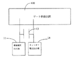
図4は本発明の液晶ディスプレイゲート駆動電圧制御装置の第2の実施例の構成を示す模式図である。図4に示すように、本発明の第2の実施例の液晶ディスプレイにおけるゲート駆動電圧制御装置は、導通電圧出力端11、カットオフ電圧出力端14及び電気容量13を備える。導通電圧出力端11とカットオフ電圧出力端14とが電気容量13によって結合する。具体的には、電気容量13の一端が導通電圧出力端11とゲート駆動回路100とに接続し、電気容量13の他端がカットオフ電圧出力端14とゲート駆動回路100とに接続する。
それで、カットオフ電圧出力端14が出力したVoffを導通電圧出力端11が出力したVonの基準電圧にして、VoffとVonとを互いに連動してVoffの収差がVonを影響する。それによって、VonがVoffに類似の波形収差を有する。従ってVonとVoffの差ΔVgが相対的に安定な値を保持できるため、相応の液晶ディスプレイのY-Block現象が改善できる。
FIG. 4 is a schematic diagram showing the configuration of the second embodiment of the liquid crystal display gate drive voltage control apparatus of the present invention. As shown in FIG. 4, the gate drive voltage control device in the liquid crystal display according to the second embodiment of the present invention includes a conduction voltage output terminal 11, a cut-off
So, in the reference voltage V on that output V off the cut-off
図5は本発明の液晶ディスプレイゲート駆動電圧制御装置の第1の実施例と第2の実施例を採用するときに生じる電圧の波形図である。図5において、aが第1のゲート駆動回路のVoffの波形であり、bが第2のゲート駆動回路のVoffの波形であり、d1が第2の第1のゲート駆動回路のVonの波形であり、d2が第2の第2のゲート駆動回路のVonの波形である。ΔVg−1’が第1のゲート駆動回路のΔVgであり、ΔVg−2’が第2のゲート駆動回路のΔVgである。図4に示すように、設置された電気容量などのような制御回路が与えた影響によって、VoffまたはVcomの波形がVonを影響してΔVg−1’とΔVg−2’とを近くするため、明らかなΔVpの変化が生じなく、相応に液晶ディスプレイのY-block現象も改善される。
本発明は1つの電気容量を有する簡単な回路で発明の目的を実現したが、共通電圧またはカットオフ電圧の収差が導通電圧を影響して導通電圧を共通電圧またはカットオフ電圧に類似する波形収差を有するようにし、各ゲート駆動回路の間のΔVgの差を解除する各回路接続方法、例えば、RC回路はいずれも本発明の保護範囲内に属する。
本発明のもう1つの実施例が液晶ディスプレイを提供した。該液晶ディスプレイは、例えば、図3または図4の液晶ディスプレイおけるゲート駆動電圧制御装置を備える。
以上の実施例は本発明の技術案を説明するものに過ぎず、限定的なものではない。より良い実施例を参照しながら本発明を詳しく説明したが、当業者が分かるべきは、本発明の技術案を補正または均等な変更をすることができ、この補正または均等な変更によって補正後の技術案を本発明の技術案の精神と範囲から逸脱することができない。
FIG. 5 is a waveform diagram of voltages generated when the first and second embodiments of the liquid crystal display gate drive voltage control apparatus of the present invention are employed. In FIG. 5, a is V off of the waveform of the first gate drive circuit, b is a V off of the waveform of the second gate drive circuit, d1 is V on the second of the first gate drive circuit Where d2 is the waveform of V on of the second second gate drive circuit. [Delta] V g-1 'is a [Delta] V g of the first gate drive circuit, [Delta] V g-2' is a [Delta] V g of the second gate drive circuit. As shown in FIG. 4, due to the influence of the control circuit such as the installed electric capacity, the waveform of V off or V com affects V on and ΔV g−1 ′ and ΔV g−2 ′ Therefore, there is no obvious change in ΔV p and the Y-block phenomenon of the liquid crystal display is improved accordingly.
Although the present invention achieves the object of the invention with a simple circuit having one electric capacity, the aberration of the common voltage or the cutoff voltage affects the conduction voltage, and the waveform aberration is similar to the common voltage or the cutoff voltage. to have a respective circuit connection method for releasing a difference [Delta] V g between the gate drive circuits, for example, both RC circuits are within the scope of the present invention.
Another embodiment of the present invention provided a liquid crystal display. The liquid crystal display includes, for example, the gate drive voltage control device in the liquid crystal display of FIG. 3 or FIG.
The above embodiments are merely illustrative of the technical solutions of the present invention and are not limiting. Although the present invention has been described in detail with reference to better embodiments, it should be understood by those skilled in the art that the technical solution of the present invention can be corrected or equivalently changed, and this correction or equivalent change can be made after correction. The technical solution cannot depart from the spirit and scope of the technical solution of the present invention.
100 ゲート駆動回路
11 導通電圧出力端
12 共通電圧出力端
13 電気容量
14 カットオフ電圧出力端
DESCRIPTION OF
Claims (9)
導通電圧とカットオフ電圧をゲート駆動回路にそれぞれ出力する導通電圧出力端とカットオフ電圧出力端と、
前記導通電圧出力端に結合し、前記導通電圧に前記カットオフ電圧に対応する波形変化を生じさせるように前記導通電圧の波形に影響を与える制御回路と、
前記カットオフ電圧に対応する波形変化を有する共通電圧を出力する共通電圧出力端と、を備え、
前記制御回路は、一端が前記導通電圧出力端に接続され、且つ、他端が前記共通電圧出力端に接続されるように設置され、前記導通電圧出力端と前記共通電圧出力端とを結合し、前記共通電圧の波形変化が前記導通電圧を影響するようにする。 A gate drive voltage control device in a liquid crystal display,
A conduction voltage output terminal and a cutoff voltage output terminal for outputting the conduction voltage and the cut-off voltage to the gate drive circuit, respectively;
A control circuit coupled to the conduction voltage output to influence the waveform of the conduction voltage so as to cause a waveform change corresponding to the cutoff voltage in the conduction voltage;
A common voltage output terminal for outputting a common voltage having a waveform change corresponding to the cut-off voltage,
The control circuit is installed such that one end is connected to the conduction voltage output end and the other end is connected to the common voltage output end, and the conduction voltage output end and the common voltage output end are coupled to each other. The waveform change of the common voltage affects the conduction voltage.
導通電圧とカットオフ電圧をゲート駆動回路にそれぞれ出力する導通電圧出力端とカットオフ電圧出力端と、
前記導通電圧出力端に結合し、前記導通電圧に前記カットオフ電圧に対応する波形変化を生じさせるように前記導通電圧の波形に影響を与える制御回路と、を備え、
前記制御回路は、一端が前記導通電圧出力端に接続され、且つ、他端が前記カットオフ電圧出力端に接続されるように設置され、前記導通電圧出力端と前記カットオフ電圧出力端とを結合し、前記カットオフ電圧の波形変化が前記導通電圧を影響するようにする。 In a gate drive voltage controller in a liquid crystal display,
A conduction voltage output terminal and a cutoff voltage output terminal for outputting the conduction voltage and the cut-off voltage to the gate drive circuit, respectively;
A control circuit coupled to the conduction voltage output and affecting the waveform of the conduction voltage so as to cause a waveform change corresponding to the cutoff voltage in the conduction voltage; and
The control circuit is installed such that one end is connected to the conduction voltage output end and the other end is connected to the cut-off voltage output end, and the conduction voltage output end and the cut-off voltage output end are connected to each other. In combination, a change in the waveform of the cutoff voltage affects the conduction voltage.
Applications Claiming Priority (2)
| Application Number | Priority Date | Filing Date | Title |
|---|---|---|---|
| CN200910079907A CN101833922A (en) | 2009-03-12 | 2009-03-12 | Control device of grid driving voltage of liquid crystal display |
| CN200910079907.0 | 2009-03-12 |
Publications (3)
| Publication Number | Publication Date |
|---|---|
| JP2010217892A JP2010217892A (en) | 2010-09-30 |
| JP2010217892A5 JP2010217892A5 (en) | 2013-04-25 |
| JP5877625B2 true JP5877625B2 (en) | 2016-03-08 |
Family
ID=42717976
Family Applications (1)
| Application Number | Title | Priority Date | Filing Date |
|---|---|---|---|
| JP2010056112A Expired - Fee Related JP5877625B2 (en) | 2009-03-12 | 2010-03-12 | Gate drive voltage controller for liquid crystal display |
Country Status (4)
| Country | Link |
|---|---|
| US (1) | US8531445B2 (en) |
| JP (1) | JP5877625B2 (en) |
| KR (1) | KR101167698B1 (en) |
| CN (1) | CN101833922A (en) |
Families Citing this family (2)
| Publication number | Priority date | Publication date | Assignee | Title |
|---|---|---|---|---|
| CN104835467B (en) | 2015-05-21 | 2017-04-05 | 京东方科技集团股份有限公司 | A kind of driving method and its device, display device |
| WO2019123514A1 (en) * | 2017-12-18 | 2019-06-27 | 堺ディスプレイプロダクト株式会社 | Display device |
Family Cites Families (7)
| Publication number | Priority date | Publication date | Assignee | Title |
|---|---|---|---|---|
| JPH09218388A (en) * | 1996-02-09 | 1997-08-19 | Hosiden Corp | Liquid crystal display device |
| KR100264161B1 (en) | 1997-09-23 | 2000-08-16 | 구본준 | Liquid crystak panel with bypass capacitor thereon |
| JP4040168B2 (en) * | 1998-05-01 | 2008-01-30 | ティーピーオー ホンコン ホールディング リミテッド | Liquid crystal display |
| KR20020017322A (en) * | 2000-08-29 | 2002-03-07 | 윤종용 | Control signal part and liquid crystal disply including the control signal part |
| KR100620139B1 (en) * | 2003-08-01 | 2006-09-13 | 비오이 하이디스 테크놀로지 주식회사 | A method for controlling the gate drving voltage in LCD |
| KR20080011896A (en) | 2006-08-01 | 2008-02-11 | 삼성전자주식회사 | Gate on voltage generation circuit and gate off voltage generation circuit and liquid crystal display having the same |
| KR101329288B1 (en) * | 2007-11-13 | 2013-11-14 | 삼성디스플레이 주식회사 | Transistor for driving gate line and liquid crystal display comprising the same |
-
2009
- 2009-03-12 CN CN200910079907A patent/CN101833922A/en active Pending
-
2010
- 2010-03-11 US US12/722,154 patent/US8531445B2/en active Active
- 2010-03-12 JP JP2010056112A patent/JP5877625B2/en not_active Expired - Fee Related
- 2010-03-12 KR KR1020100022309A patent/KR101167698B1/en active IP Right Grant
Also Published As
| Publication number | Publication date |
|---|---|
| KR101167698B1 (en) | 2012-07-20 |
| US8531445B2 (en) | 2013-09-10 |
| JP2010217892A (en) | 2010-09-30 |
| KR20100103422A (en) | 2010-09-27 |
| US20100231572A1 (en) | 2010-09-16 |
| CN101833922A (en) | 2010-09-15 |
Similar Documents
| Publication | Publication Date | Title |
|---|---|---|
| US10354605B2 (en) | Liquid crystal display and method for manufacturing the same | |
| US8228287B2 (en) | Liquid crystal display device for removing ripple voltage and method of driving the same | |
| KR100759974B1 (en) | A liquid crystal display apparatus and a driving method thereof | |
| US8289255B2 (en) | Electro-optical apparatus and display thereof | |
| KR20020057408A (en) | liquid crystal display system, panel and method for compensating gate line delay | |
| US8854291B2 (en) | Gate signal line driving circuit for supressing noise in a gate signal in a display device | |
| WO2013143195A1 (en) | Feed-through voltage compensation circuit, liquid crystal display device and feed-through voltage compensation method | |
| JP5255751B2 (en) | Driving device for liquid crystal display device and liquid crystal display device having the same | |
| US7995051B2 (en) | Driving circuit, driving method and liquid crystal display using same | |
| US20110019118A1 (en) | Liquid crystal display device | |
| US7671930B2 (en) | Liquid crystal display pixel structure having sub-pixels with particular capacitance | |
| US20080122875A1 (en) | Liquid crystal display device and driving circuit and driving method of the same | |
| KR20110054384A (en) | Liquid crystal display | |
| US20120112193A1 (en) | Transistor array substrate | |
| US20090002305A1 (en) | Liquid crystal display with common voltage generator for reducing crosstalk | |
| WO2013152515A1 (en) | Liquid crystal display device and display panel thereof | |
| JP5877625B2 (en) | Gate drive voltage controller for liquid crystal display | |
| US20060158407A1 (en) | Liquid crystal display device, driving circuit and driving method thereof | |
| US20130162508A1 (en) | Driving Circuit of a Liquid Crystal Panel and an LCD | |
| KR101992852B1 (en) | Display device | |
| KR101668261B1 (en) | Liquid crystal display device and method of fabricating the same | |
| US9664970B2 (en) | LCD panel wherein TFT units to mitigate gate signal delay are disposed opposite to the gate driver and connected to individual gate lines | |
| US20130321367A1 (en) | Display device | |
| KR100438966B1 (en) | A liquid crystal display device applying common voltage having different phase and a method of operating thereof | |
| US11347122B2 (en) | Display apparatus |
Legal Events
| Date | Code | Title | Description |
|---|---|---|---|
| A521 | Request for written amendment filed |
Free format text: JAPANESE INTERMEDIATE CODE: A523 Effective date: 20130311 |
|
| A621 | Written request for application examination |
Free format text: JAPANESE INTERMEDIATE CODE: A621 Effective date: 20130311 |
|
| A977 | Report on retrieval |
Free format text: JAPANESE INTERMEDIATE CODE: A971007 Effective date: 20130821 |
|
| A131 | Notification of reasons for refusal |
Free format text: JAPANESE INTERMEDIATE CODE: A131 Effective date: 20130903 |
|
| A521 | Request for written amendment filed |
Free format text: JAPANESE INTERMEDIATE CODE: A523 Effective date: 20131129 |
|
| A131 | Notification of reasons for refusal |
Free format text: JAPANESE INTERMEDIATE CODE: A131 Effective date: 20140804 |
|
| A521 | Request for written amendment filed |
Free format text: JAPANESE INTERMEDIATE CODE: A523 Effective date: 20141104 |
|
| A02 | Decision of refusal |
Free format text: JAPANESE INTERMEDIATE CODE: A02 Effective date: 20150501 |
|
| A521 | Request for written amendment filed |
Free format text: JAPANESE INTERMEDIATE CODE: A523 Effective date: 20150827 |
|
| A911 | Transfer to examiner for re-examination before appeal (zenchi) |
Free format text: JAPANESE INTERMEDIATE CODE: A911 Effective date: 20150903 |
|
| TRDD | Decision of grant or rejection written | ||
| A01 | Written decision to grant a patent or to grant a registration (utility model) |
Free format text: JAPANESE INTERMEDIATE CODE: A01 Effective date: 20160104 |
|
| A61 | First payment of annual fees (during grant procedure) |
Free format text: JAPANESE INTERMEDIATE CODE: A61 Effective date: 20160126 |
|
| R150 | Certificate of patent or registration of utility model |
Ref document number: 5877625 Country of ref document: JP Free format text: JAPANESE INTERMEDIATE CODE: R150 |
|
| R250 | Receipt of annual fees |
Free format text: JAPANESE INTERMEDIATE CODE: R250 |
|
| R250 | Receipt of annual fees |
Free format text: JAPANESE INTERMEDIATE CODE: R250 |
|
| R250 | Receipt of annual fees |
Free format text: JAPANESE INTERMEDIATE CODE: R250 |
|
| R250 | Receipt of annual fees |
Free format text: JAPANESE INTERMEDIATE CODE: R250 |
|
| LAPS | Cancellation because of no payment of annual fees |